1
Stability of TaC Diffusion Barrier Between Si and Cu
Tomi Laurila, Kejun Zeng, and Jorma K. Kivilahti
Laboratory of Electronics Production Technology, Helsinki University of Technology,
P.O. Box 3000, FIN-02015 HUT, Finland
Jyrki Molarius and Ilkka Suni
VTT Microelectronics, FIN-02044 VTT, Finland
ABSTRACT
The reaction mechanisms and related microstructures in the Si/TaC/Cu
metallization system have been studied experimentally and theoretically by utilizing ternary
Si-Ta-C, Ta-C-Cu and Ta-C-O phase diagrams as well as calculated activity diagrams.
With the help of sheet resistance measurements, Rutherford backscattering spectrometry, x-
ray diffraction, scanning electron microscopy, and transmission electron microscopy, the
metallization structure with the 70 nm thick TaC barrier layer was observed to fail
completely at temperatures above 725 °C because of the formation of large Cu3Si
protrusions. However, the formation of amorphous Ta layer containing significant amounts
of carbon and oxygen was already observed at the TaC/Cu interface at 600 °C. This layer
also constituted an additional barrier layer for Cu diffusion, which occurred only after the
crystallization of the amorphous layer. The formation of Ta2O5 was observed at 725 °C
with x-ray diffraction, indicating that the oxygen rich amorphous layer had started to
crystallize. The formation of SiC and TaSi2 occurred almost simultaneously at 800 °C. The
observed reaction structure was consistent with the thermodynamics of the ternary systems.
The metallization structures with 7 nm and 35 nm TaC barrier layers failed above 550 °C
and 650 °C, respectively, similarly because of the formation of Cu3Si. The high formation
temperature of TaSi2 and SiC implies high stability of Si/TaC interface, thus making TaC
layer a potential candidate to be used as a diffusion barrier for Cu metallization.

2
I. INTRODUCTION
As dimensions of solid state devices are scaled down, the continuing demand for
improvement in the performance of interconnects has led to the need to replace currently
used aluminum based conductors with materials that have better electrical properties.
Moreover, the reliability of aluminum based conductors is limited by the relatively poor
electromigration resistance of the material. Copper has attracted increasing attention as a
"state-of-the-art" metallization material because of its better electrical properties as well as
better electromigration resistance in comparison to aluminium.1,2 Unfortunately, the
interaction between Si and Cu is strong and detrimental to the electrical performance of Si
even at temperatures below 200 °C.3-6 Therefore, it is necessary to implement a barrier
layer between Si and Cu. Ta and Ta-based diffusion barriers have been the subject of
numerous investigations.7-17 They fulfill rather well the overall requirements for diffusion
barriers as summarized by Nicolet.18 Among the most promising candidates to be used for
this purpose are the binary tantalum nitrides and carbides. Whereas Ta-nitrides have been
investigated widely, only few known reports have been published about TaC- based
diffusion barriers.16,17 Hence, there is a clear need for further investigation of these
diffusion barrier layers, since they seem to offer a viable solution to the barrier layer
problem associated with Cu metallization.
There exist two stable carbides in the Ta-C system, Ta2C and TaC, with melting
points of 3330 °C and 3985 °C, respectively.19 Since both carbides are interstitial
compounds and thermally very stable20, the stability of Si/TaC interface, as compared for
example to Si/Ta interface, is expected to increase because of the elevated formation
temperature of tantalum silicides. Further, because no stable carbides exist in the Cu-C
system, the interface between TaC and Cu should be stable. Moreover, based on the
evaluated Ta-C-Cu ternary phase diagram, Cu is in thermodynamic equilibrium with both
carbides.21 However, Cu is eventually expected to penetrate through the barrier layer owing
to its high affinity towards Si. Thus, the failure mechanism is most likely a combination of
tantalum silicide formation at Si/TaC interface and diffusion of Cu through the barrier layer
with accompanied Cu3Si formation at the same Si/TaC interface.

3
In the present study, the reactions in the Si/TaC/Cu metallization system are
investigated experimentally and theoretically by utilizing a combined thermodynamic-
kinetic approach. Although the complete thermodynamic equilibria are hardly ever
encountered in thin film systems, the local equilibrium is, however, generally attained at
interfaces. Therefore, the phase diagrams provide us with an efficient method for designing
diffusion barrier layers between various metallizations, especially when they can be
combined with kinetic information. The phase relations in the system are examined by
combining the assessed binary data into ternary thermodynamic descriptions. By employing
the same thermodynamic data activity diagrams will also be calculated. The information
extracted from these diagrams are used together with the experimental results obtained to
discover the underlying mechanism(s) for the failure. It is expected that by employing this
approach better understanding of the equilibria and reactions in the system is achieved.
II. EXPERIMENT
The copper and tantalum carbide films were sputtered onto cleaned and oxide-
stripped (100) n-type Si substrates in a dc/rf-magnetron sputtering system. The deposition
of TaC was obtained from the TaC-target (hot-pressed, 6.2 wt-% of C, main impurity Nb ~
0.3 wt-%) in argon atmosphere. The pressure before the deposition runs was approximately
10-5 Pa. The thickness of the tantalum carbide layers was 70 nm. The copper films with
thickness of 400 nm were subsequently sputter-deposited without breaking the vacuum. In
order to investigate the effect of the barrier thickness on the stability of the metallization
structure, another set of samples with thinner tantalum carbide (7 nm and 35 nm) and
copper layers (100 nm) were fabricated. The samples were annealed under the vacuum of
10-4 Pa at temperatures ranging from 500 °C to 800 °C for 30 minutes.
The sheet resistance measurements at room temperature by using a four-point probe
were used to detect possible interfacial reactions after the each annealing step. The reaction
products in the Si/TaC/Cu metallization schemes were characterized by x-ray diffraction
(XRD), Rutherford backscattering spectrometry (RBS) and the transmission electron
microscopy (TEM). Surfaces of the samples were also examined with an optical
microscope and scanning electron microscope (SEM). XRD analyses were conducted with
a Bruker axs D8 Advance diffractometer. Both fixed 1deg. incoming angle and theta-2theta

4
measurements were carried out with a measurement range of 20-60 ° (2θ). The RBS
measurements were performed with a 2 MeV He+ ion beam normal to the surface, with a
scattering angle of 170 °. The TEM investigations were conducted with JEOL 2000FX
analytical TEM/STEM operated at 200 kV. A few micrographs were taken also at 400 kV
acceleration voltage (JEM-4010). SEM investigations were performed with a JEOL JSM-
6335F field emission scanning electron microscope operated at 15 kV. The results of the
experimental investigations were compared with the assessed phase diagrams. Ternary Si-
Ta-C, Ta-C-Cu and Ta-C-O phase diagrams as well as the corresponding activity diagrams
were evaluated from the assessed binary thermodynamic data.
III. RESULTS
The sheet resistance of the layered metallization structure as a function of
temperature is displayed in Fig. 1.
0
10
20
30
40
50
60
70
0 200 400 600 800
u7 nm35 nm70 nm
Temperature (oC)
Shee
t res
ista
nce
(Ohm
s/sq
uare
)
Fig. 1. Sheet resistance vs. temperature curve of the Si/TaC/Cu metallization structures
with different TaC layer thickness annealed for 30 min at different temperatures.
At 775 °C there is an abrupt rise in the curve of the sample with the 70 nm thick
TaC film, showing that some reaction has occurred in the metallization system. Above 775
°C, the sheet resistance starts to decrease. Thus, the structure behaves like an intrinsic
semiconductor. This suggests that reaction products with high resistivity have been formed,
since the underlying silicon is now carrying almost the entire probe current. The thin 7 nm
Cu3Si

5
and 35 nm TaC layers are stable up to 550 °C and 650 °C, respectively, as determined by
the sheet resistance measurements (Fig. 1). It must be realized, however, that the sheet
resistance measurements monitor chiefly the state of the Cu overlayer, since it carries
almost the entire probe current. Thus, interaction between other layers, e.g. TaC and Si,
may not be immediately detected with this technique.
The surfaces of the thick (70nm) samples maintain a shiny copper-like appearance
up to 750 °C and the 7 nm and 35 nm samples up to 550 °C and 650 °C, respectively. The
SEM micrograph of the surface structure of the sample with 70 nm thick TaC barrier
annealed at 800 °C is shown in Fig. 2. As can be seen, large "squares" (approximately 20-
30 µm in diagonal) have formed on the surface. These defects seem to be composed totally
out of one phase. There is also comparable phase distributed around the central "square" in
Fig. 2, as pointed out by the similar contrast (represented by an arrow in Fig. 2). These
"squares" are surrounded by a "flowery" patterned structure, which seems to be a two phase
structure where one phase is embedded into the other. Some of this "flowery" pattern can
also be seen inside the large "squares". The structures seen on the surface of the samples
are similar to those observed earlier to be associated with the failure of the Ta barrier layers
and the formation of Cu3Si and TaSi2.22
Fig. 2. SEM micrograph from the surface of the Si/TaC(70nm)/Cu(400nm) sample
annealed at 800 °C for 30 min. The arrow shows the phase around the "squares" which
seems to be the same as the bulk of the individual "squares".

6
0
5000
10000
15000
20000
25000
0 100 200 300 400 500Channel number
RB
S yi
eld
(cou
nts/
chan
nel)
600 oC600 oC
725 oC725 oC
0
5000
10000
15000
20000
25000
30000
35000
0 100 200 300 400 500 600
Si Cu Ta
0.5 1.0 1.5 2.0
E(MeV)
Si Cu Ta
0.5 1.0 1.5 2.0
E(MeV)
a)
b)
Fig. 3. RBS spectra (2.0 MeV 4 He+, θ = 170 °) from the Si/TaC(70nm)/Cu(400nm)
samples a) no annealing and b) annealed at different temperatures for 30 min. Vertical
arrows represent surface scattering energies.
The RBS analyses of the as-deposited samples show sharp edges of the elements in the
spectra, thus showing no intermixing between the layers before the annealings (Fig. 3 a).
Fitting the measured RBS data to GISA 3.99 simulations23,24 reveals that the TaC layer
thicknesses are 7 nm, 35 nm and 70 nm for the three types of sample, respectively. The
thicknesses were obtained by using the bulk atomic densities. The composition of the Ta-C
layers is slightly rich with respect to carbon, Ta48C52. Even when taking into account errors
in the measurements and in the simulations,24 this deviation can not be attributed solely to
experimental error. Shifts in stoichiometry in TaC have been observed to take place only
towards the Ta-rich side (i.e. C defiant carbides)20, and therefore the slight excess of carbon
implies that graphite precipitation may occur during the annealings. RBS measurements of
the annealed samples showed clearly discrete layers with no intermixing up to 550 °C.
However, at 600 °C the RBS spectrum suggests that interdiffusion of Ta and Cu takes place
(Fig. 3 (b)). As can be seen, some tantalum moves to the surface. In addition the trailing
edge of the Cu and leading edge of the Si signals are smoothened, suggesting some

7
intermixing. The temperature where the degradation of the layers starts according to the
RBS is unexpectedly low. However, if the slight excess of carbon in the TaC films results
in segregation to the grain boundaries as expected, this may open short circuit diffusion
paths for Cu and Si atoms via the most likely amorphous graphite media located in the
grain boundaries. Similar failure mechanism in carbon rich TaC films was also suggested
by Imahori et.al.16 Moreover, the TaC films are expected to contain pinholes and other
defects, which may enable interdiffusion locally at considerably low temperatures.
Therefore, despite the overall stability of the TaC layers, it seems that the layers have weak
spots where the mixing occurs already at low temperatures. From the backscattering spectra
taken at higher temperatures, for example at 725 °C, it is very difficult to obtain more
information about the reactions taking place, since the spectra become quite complex.
Nevertheless, as can be seen from Fig. 3, more Ta moves to the surface and the Cu and Si
interfaces degrade further, showing more severe intermixing.
In order to obtain more information about the phase formation during the
annealings, XRD analyses were carried out. Both fixed 1 deg. incoming angle and theta-
2theta configurations were used. The results shown are a combination of both types of
measurements. The analyses show that up to 725 °C only TaC and Cu are present in the
samples with the 70 nm TaC barrier layer (see Fig. 4). Further, no reaction products are
detected at 600 °C with XRD. At 725 °C there are some diffractions from Ta2O5, denoting
the presence of oxygen in the annealing environment and in the films themselves. At 750
°C, the formation of copper silicide, Cu3Si, takes place according to the XRD. However,
the analyses show that the structure of the Cu3Si is not equilibrated, since the peaks are not
"stable", i.e. they change their position slightly with changing temperature. This can be
explained by the fact that Cu3Si has at least three crystal structures stable in different
temperature ranges19,25,26, and the given phase may still be in tranformation. Moreover, it
has been observed earlier that the peak positions change slightly if the samples are kept at
room temperature for a prolonged time.25 No other silicides are detected at this temperature
with XRD. At 800 °C, the TaC, Cu, and Ta2O5 peaks disappear, and only Cu3Si and TaSi2
peaks are present. The samples with the 7 nm TaC barrier layer show only Cu peaks up to
550 °C (Fig. 5). The reason for this is most likely that the very thin (7 nm) TaC layer is in
nanocrystalline (i.e. nearly amorphous) state.

8
0
50
100
150
200
250
20 30 40 50 60
l
n
v
TaCCu
Cu3Si
u
rTa2O5
TaSi2
0
50
100
150
200
250
20 30 40 50 60
0
50
100
150
200
250
20 30 40 50 60
0
50
100
150
200
250
20 30 40 50 60
l
n
v
u
r
l l
l
n
n
l
n
l
n
lul
n
v
l
r
r
r
r
vv
r
r
r r
600 oC
725 oC
750 oC
800 oC
2-Theta
Arb
itrar
y un
its
Fig.4. XRD spectra from the Si/TaC(70nm)/Cu(400nm) samples annealed for 30 min at
different temperatures.

9
0
50
100
150
20 30 40 50 60
0
50
100
150
20 30 40 50 60
n
v
Cu
Cu3Si
n
v
550 oC
600 oC
n
2-Theta
Arb
itrar
y un
its
Fig.5. XRD spectra from the Si/TaC(7nm)/Cu(100nm) samples annealed for 30 min at
different temperatures.
0
50
100
150
20 30 40 50 60
0
50
100
150
20 30 40 50 60
l
n
v
TaCCu
Cu3Si
l
n
v
ln
l
l
n
nv
650 oC
675 oC
2-Theta
Arb
itrar
y un
its
Fig.6. XRD spectra from the Si/TaC(35nm)/Cu(100nm) samples annealed for 30 min at
different temperatures.

10
Similar results indicating the amorphous nature of sputter-deposited TaC films have
similarly been reported by Tsai et al.17 The formation of Cu3Si occurs at 600 °C in these
samples as displayed in Fig. 5. The samples with the 35 nm TaC barrier layer show both
TaC and Cu peaks up to 650 °C (Fig. 6). The formation of Cu3Si takes place at 675 °C. At
the temperature of formation of Cu3Si, there is still some TaC left in the 35 nm sample. No
trace of TaSi2 is found in the thin 7 nm and 35 nm samples annealed up to 700 °C and 725
°C, respectively. Despite the different thicknesses of the films, the failure seems to be
induced by Cu penetration through the TaC layer and the formation of Cu3Si, at least
according to the XRD analyses. The Si/TaC interface is relatively stable, since no reaction
is observed below 800 °C.
To clarify the puzzling RBS results from the samples annealed at 600 °C a cross-
sectional TEM analysis was performed. The view from the 70 nm thick sample annealed at
600 °C for 30 minutes is presented in Fig. 7, which shows unambiguously the presence of
an amorphous layer between TaC and Cu. The amorphous structure of the interlayer can be
seen more clearly from the high resolution micrograph presented in Fig. 8.
TaC50 nm
a-Ta[O,C]x
Cu
Fig.7. Bright field TEM micrograph from the Si/TaC(70nm)/Cu(400nm) sample annealed
at 600 °C for 30 min.

11
Cu
TaC
a-Ta[O,C]x
Fig.8. HREM micrograph from the amorphous Ta[C,O]x phase from the sample annealed at
600 °C for 30 min.
The amorphous nature of the layer was further confirmed with electron diffraction
patterns (not shown here). The composition of the layer was analyzed from the very thin
foil (tens of nanometers thick) with the energy dispersive spectroscopy (EDS) in the
analytical TEM to be Ta with noticeable amounts of oxygen and carbon. As high amounts
of oxygen and carbon were present only within the amorphous layer. The layer is most
probably Ta[O,C]x (i.e. metastable oxide) containing some carbon released from the partly
dissociated TaC layer. The amorphous layer also explains why the XRD was unable to
detect reaction product formation at 600 °C and gives some indication why the RBS
spectrum had already degraded at 600 °C.

12
Cu3Si
Cu3Si
Si-OCu
Cu
Si-O
Si-O
Si-O
SiTaC
300 nm
CuTaOx
Fig.9. Bright field TEM micrograph from the Si/TaC(70nm)/Cu(400nm) sample annealed
at 750 °C for 30 min.
The XTEM micrograph of the sample with a 70 nm TaC barrier layer annealed at
750 °C for 30 minutes is shown in Fig. 9. Here, one can clearly see the formation of large
triangular grain, which was identified with the combination of the EDS and the electron
diffraction analyses as slightly Si defiant Cu3Si phase. The size of the protrusion is
considerably smaller than observed from the sample annealed at 800 °C (see Figs. 2 and
11), indicating that the reaction continues to advance and the defect is expected to grow. It
is evident from the micrograph that the phase has a cellular appearance, but the origin of
this is not yet clear. The cellular structure may be a result of the fact that Cu3Si is still under
microstructural evolution, as mentioned above. The hemispherical grain above the
triangular grain was identified as Si deficient Cu3Si, again with the similar cellular
appearance. These two defects will most probably "combine" at higher temperatures (~ 800
°C) by conventional Ostwald ripening to form the observed larger defects. Between these
two grains, there is a region composed of Si-O, Cu-Si, and Ta-rich phases. The Ta-rich film
shown in Fig. 9 is actually a 2-phase structure with TaC at the bottom of the film and
crystalline TaOx phase (expected to be Ta2O5 as detected also with the XRD) at the upper
part of the film. There are also some remains from the Cu film between the two Cu3Si

13
grains, as suggested by the XRD analysis taken at the same temperature (see Fig.4). No
continuous TaC film is seen in this micrograph, which suggests that the rupture of the
barrier layer has taken place. However, as can be seen from the micrograph taken at the
same temperature from a different location (Fig. 10), the TaC/TaOx bilayer is still present at
other sites. The formation of the Cu3Si protrusion seen in the micrograph occurs because of
the diffusion of Cu through the barrier most probably via the grain boundaries of the TaC
layer. The crystalline nature of the bilayered structure is also clearly seen in this
micrograph.
0.2 mµ
Cu
Cu3Si TaCTaOx
Fig.10. Bright field TEM micrograph from the Si/TaC(70nm)/Cu(400nm) sample annealed
at 750 °C for 30 min.
In Fig. 11, an "overall" view of the TEM cross-section of the sample annealed at
800 °C through one of the "squares" and the "flowery" pattern (see Fig. 2) is presented.
The cross-section is inverted (vertically), thus the original top surface seen in Fig. 2 is at the
bottom in this micrograph.

14
Silicon
"Flowery" pattern
"Square"12
2 µm
Fig. 11. Bright field TEM micrograph from the Si/TaC(70nm)/Cu(400nm) sample annealed
at 800 °C for 30 min.
TaSi2 "flower"
a-SiOx
SiC
Cu-Si
300 nm
Fig.12. Bright field TEM micrograph from the Si/TaC(70nm)/Cu(400nm) sample annealed
at 800 °C for 30 min corresponding to � in Fig.11.
A more detailed, magnified view of the area marked as � in Fig. 11 can be seen in Fig. 12.
It shows that the "flowery" pattern seen from the top in Fig. 2 is in fact TaSi2, as determined
by a combination of elemental analyses with the EDS and diffraction pattern analysis.
However, the overall structure of the reaction product layers is somewhat complex. On the

15
top surface, there is a very thin amorphous SiOx layer. Below this top layer are the TaSi2
grains. Between the two TaSi2 grains seen in the micrograph, there is a Cu-rich region that
contains some Si. This was expected to be Cu3Si, but it was not possible to confirm it
unambiguously owing to the very small amount of the phase present. This is the phase that
can be seen from the top in Fig. 2 around the central "square" (the arrow in Fig. 2) and is
considered to be the same phase as the "squares" themselves. Below the TaSi2 grains, there
is again the same Cu-rich layer that was observed between the TaSi2 grains. Beneath this
layer, there is another layer composed of Si and C with some Cu. This seems to be a
mixture of Cu-rich phase and SiC. The presence of SiC is expected based on a combination
of kinetic and thermodynamic considerations (see the discussion below). The region
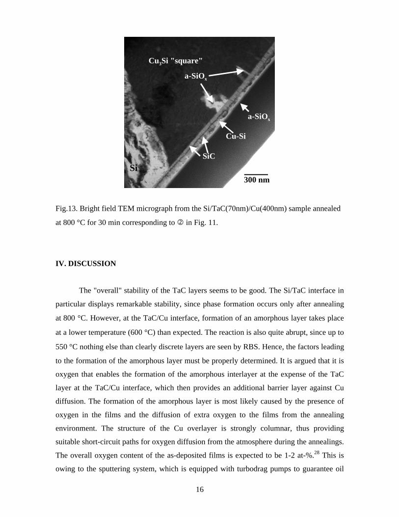
marked as � in Fig. 11 is shown in more detail in Fig. 13. As shown in the micrograph, the
"bulk" of the very large "square" is Cu3Si. The composition of the phase was verified with
EDS to be ~ 25 at-% of Si. However, the structure of the phase is somewhat peculiar.
According to the CBED (convergent beam electron diffraction) pattern taken along the
[0001] zone axis, the phase is hexagonal and not orthorhombic as suggested by Solberg.26
However, as the hexagonal structure can be viewed as a sublattice of an orthorhombic unit
cell, the entire structure can be viewed as a two-dimensional long-period superlattice
composed of several domains.26 The structure is probably best depicted as a 3x1
superlattice.27 This observation of the somewhat unusual structure of the Cu3Si helps one
understand the XRD analyses, where it was difficult to find a good fit for the Cu3Si peaks.
The layered structure around the large "square" shows again the thin amorphous SiOx layer
on the surface. Some amorphous SiOx is also present as spikes inside the large Cu3Si
"precipitate". No Ta2O5 is detected at this temperature and it is anticipated that it has been
dissociated because of the formation of a-SiOx and TaSi2. Beneath the top layer, there is
another layer composed of SiC grains and Cu-rich layer, which acts as a "cement" between
the SiC grains. This is the same type of Cu-rich layer that was seen in Fig. 12 between the
TaSi2 grains and is again most likely Cu3Si. Below this mixed layer, there is again a layer
of SiC. The "flowery" pattern inside the large Cu3Si "squares" (see Fig. 2) was also
identified as TaSi2.
16
300 nm
Cu3Si "square"
SiC
Cu-Si
a-SiOx
a-SiOx
Si
Fig.13. Bright field TEM micrograph from the Si/TaC(70nm)/Cu(400nm) sample annealed
at 800 °C for 30 min corresponding to � in Fig. 11.
IV. DISCUSSION
The "overall" stability of the TaC layers seems to be good. The Si/TaC interface in
particular displays remarkable stability, since phase formation occurs only after annealing
at 800 °C. However, at the TaC/Cu interface, formation of an amorphous layer takes place
at a lower temperature (600 °C) than expected. The reaction is also quite abrupt, since up to
550 °C nothing else than clearly discrete layers are seen by RBS. Hence, the factors leading
to the formation of the amorphous layer must be properly determined. It is argued that it is
oxygen that enables the formation of the amorphous interlayer at the expense of the TaC
layer at the TaC/Cu interface, which then provides an additional barrier layer against Cu
diffusion. The formation of the amorphous layer is most likely caused by the presence of
oxygen in the films and the diffusion of extra oxygen to the films from the annealing
environment. The structure of the Cu overlayer is strongly columnar, thus providing
suitable short-circuit paths for oxygen diffusion from the atmosphere during the annealings.
The overall oxygen content of the as-deposited films is expected to be 1-2 at-%.28 This is
owing to the sputtering system, which is equipped with turbodrag pumps to guarantee oil

17
free deposition and therefore the pumping of water vapor from the chamber is not very
efficient, although system has load-lock. The major part of the incorporated oxygen is most
likely present at the grain boundaries of the as-deposited TaC layer, since no extensive
solubility of Ta2O5 into TaC is expected. During the annealings oxygen dissolves into the
TaC matrix from the grain boundaries.
In principle, to investigate the reactions in the present system, the thermodynamic
description of the five-component Si-Ta-C-O-Cu system should be carried out. This implies
the carefully assessed data on ten binary systems, ten ternary systems, and five quaternary
systems. Unfortunately, there are no adequately reliable data on all the multicomponent
systems required. Therefore, the reactions at the Si/TaC and TaC/Cu interfaces are
examined with the help of the assessed Si-Ta-C, Ta-C-Cu and Ta-C-O ternary phase
diagrams together with the calculated activity diagram for Si (Figs. 14-17), since they alone
provide a considerable amount of useful information about the reactions.
The isothermal section of the metastable Ta-C-O phase diagram at 600 °C is
displayed in Fig.14. The oxygen partial pressure used in the calculations was 0.2×10⁻⁴ Pa.
Since no thermodynamic data for the metastable Ta-oxides are available, the data for stable
Ta2O5 phase is used.29-33 It is evident that the metastable amorphous Ta[O,C]x will
eventually transform into the stable phases (i.e. Ta2O5 and graphite). In fact, according to
the XRD-results, the formation of Ta2O5 took place at 725 °C (Fig. 4). When the formation
of Ta2O5 takes place TaC and graphite must also be present, since they form a three phase
field in the diagram (Fig. 14).

18
1/2O2
Ta C0.2 0.4 0.6 0.8 1.00
X(C)
X(O)
TaC
TaC +Ta2O5+graphiteTaC+
Ta2O5 +Ta[O]ss
0.2
0.4
0.6
0.8 Ta2O5
Ta2O5+graphite + 1/2O2
C.L.
initial composition
Fig. 14. Isothermal section from the evaluated metastable ternary Ta-C-O phase diagram at
600 °C under the external oxygen pressure of about 0.2×10⁻⁴ Pa. The tie-lines in the TaC-
Ta2O5 two phase region are shown in the diagram. The contact-line (C.L.) between the TaC
film and oxygen indicating the initial unstable equilibrium as well as the approximate
composition of the TaC[O]gb are also shown.
TaC phase is expected to come into local equilibrium with metastable Ta[O,C]x
before the formation of stable Ta2C is possible. Therefore, the formation of Ta2C has been
suppressed in the calculations to obtain the conditions of the actual metallization structure.
The initial state of the system, where the TaC is in equilibrium with the entrapped oxygen,
is marked with the contact line (C.L.) in the isothermal section, showing that the situation is
highly unstable. The initial composition is located on the contact line and inside the three
phase field (TaC + Ta2O5 + graphite) in the isothermal section. Since the overall oxygen
content is relatively low (~ 1-2 at-%) the composition lies close to the Ta-C binary system
(the anticipated composition being depicted in Fig. 14). When the TaC[O]gb films are
annealed at elevated temperatures, oxygen dissolves into the TaC matrix, resulting
ultimately in the formation of the stable Ta2O5 and graphite. However, owing to the kinetic
constraints, the direct formation of the stable tantalum oxide is not possible and the
formation of the amorphous Ta[O,C]x layer takes place. Considering the thickness of the
amorphous layer at 600 °C, it is evident that some oxygen has to be incorporated into the
films also from the annealing atmosphere. Only after the temperature raises above 700 °C

19
the relaxation of the kinetic constraints enable the formation of the stable three phase
structure (TaC + Ta2O5 + graphite).
The diffusion of copper can proceed only after the amorphous layer has crystallized.
The crystallization of the layer occurs around 750 °C, as can be seen from Fig. 10. From
the micrograph it is additionally evident that the upper part of the TaC/Ta[O,C]x bilayer is
crystalline at this temperature (probably Ta2O5 as indicated by the XRD results in Fig. 4)
and the diffusion of Cu through the barrier and the formation of Cu3Si has taken place.
Without the amorphous interlayer, the diffusion of Cu towards Si is expected to set in at
much lower temperatures, since the microstructure of the TaC layer is highly columnar.
Hence, the effect of oxygen is somewhat beneficial. However, the TEM micrographs
displayed in Figs. 9 and 10 show clearly that approximately half of the original barrier layer
is consumed by the amorphous layer before the crystallization. Hence, with thin barrier
layers the amorphous layer may consume the TaC layer completely. Even though the
thermal stability (i.e. the crystallization temperature) of the amorphous layer is expected to
be quite high, it will change the electrical and microstructural properties of the original
Si/TaC/Cu structure and can not therefore be considered beneficial. The reason for the
existence of the Ta[O,C]x layer in amorphous form at relatively high temperatures, is not
known. It is known, however, that metalloids, such as B, C, N, Si and P, can stabilize
amorphous structure in transition metals.34 Therefore, it is expected that carbon stabilizes
the amorphous structure in this system. Carbon inhibits the crystallization of the amorphous
Ta[O,C]x up to 725 °C, where the formation of Ta2O5 is observed (Fig. 10). No graphite
could be detected at 725 °C. The reason for the absence of graphite is most probably the
very difficult nucleation of the phase, as observed elsewhere.35
The ternary Si-Ta-C and Ta-C-Cu phase diagrams were evaluated from the assessed
binary thermodynamic data36-38, and are presented in Figs. 15 and 16. The question of
carbon solubility in Ta5Si3, which is expected to be substantial based on the other Me5Si3
silicides (e.g. Ti5Si3 ~10 at-%)39, must be carefully considered in the Si-Ta-C system. The
question of solubility is currently a controversial topic and has not been unambiguously
solved. Therefore, ternary carbon solubility into Ta5Si3 has not been introduced into the
ternary diagram at this stage. Schuster et al.40 stated that based on the investigations of

20
lattice parameter changes in the Ta-Si-C system, there should be no noticeable solubility of
carbon into Ta5Si3. Instead, they propose the existence of a ternary compound Ta5Si3C1-x.
C
Ta Cu0 0.2 0.4 0.6 0.8 1.0
x(Cu)
x(C)
0
0.2
0.4
0.6
0.8
1.0
TaC
Ta2C
TaC+C+Cu
Ta+Ta2C+Cu
Ta2C+TaC+CuTa2C+Cu
TaC+Cu
Fig.15. Isothermal section from the evaluated ternary Ta-C-Cu phase diagram at 800 °C.
The status of this compound is nevertheless still uncertain, since it is not clear if it is a real
ternary compound or simply the binary Ta5Si3 with ternary carbon solubility. Accordingly,
possible ternary compounds have similarly been excluded from the diagrams owing to the
lack of reliable data. The absence of ternary phases is consistent with the general situation
in the thin film systems, where ternary phases frequently have difficulties in nucleating.
Nevertheless, the possible solubility of carbon into Ta5Si3 or the existence of ternary
compounds must be experimentally verified with bulk samples, in order to establish the
solubility limits and to provide a reliable basis for the understanding of these metallization
systems.
It can be seen from the isothermal section of the assessed ternary Ta-C-Cu phase
diagram at 800 °C (Fig. 15) that Cu is in equilibrium with both tantalum carbides TaC and
Ta2C. Thus, the TaC/Cu interface is stable, since there is no driving force for reaction
between the materials. However, owing to the high affinity of Cu towards Si, it is evident
that Cu will in time penetrate through the TaC layer to react with Si. Moreover, as been
discussed above, oxygen incorporated into the films de-stabilizes the TaC/Cu interface and

21
the formation of the amorphous layer takes place. On the other hand, since the Si/TaC
interface is not in equilibrium, driving force for reaction between the substrate and the TaC
layer exists (Fig. 16). Assuming that the local equilibrium is achieved at the interfaces of
the thin film system, it is possible to use phase diagrams coupled with certain kinetic rules
to predict possible or at least to rule out impossible reaction sequences. First, the mass-
balance requires that the diffusion path, which is a line in the ternary isotherm, representing
the locus of the average compositions parallel to the original interface through the diffusion
zone41, crosses the straight line connecting the end members of the diffusion couple at least
once. Secondly, no element can diffuse intrinsically against its own activity gradient42 (i.e.
from a low chemical potential area to a high chemical potential area).
C
Ta Si
x(Si)
x(C)
0 0.2 0.4 0.6 0.8
0.8
1.0
1.0
0
0.2
0.4
0.6
TaC
Ta2C
SiC
Ta3Si Ta2Si Ta5Si3TaSi2
TaC+C+SiC
TaC+SiC+TaSi2
TaSi2+SiC+Si
Ta+Ta2C+ Ta3Si
Ta2 C+TaC+TaSi
2Ta2C+TaSi
2+Ta5Si3
C.L.
Fig.16. Isothermal section from the evaluated ternary Si-Ta-C phase diagram at 800 °C.
Contact-line between Si and TaC is marked as C.L. The diffusion path is also superimposed
into the isothermal section.
Although there exists a TaC + TaSi2 two phase region in the phase diagram (Fig.
16), SiC must be formed to incorporate the carbon released after the formation of TaSi2 in
the reaction between Si and TaC, because of the mass balance requirement. The formation
of SiC and TaSi2 was confirmed with TEM investigations and therefore gives support to the
assessed phase diagram. As shown in Fig. 12 the reacted structure consists of layers of SiC
and TaSi2 on top of the silicon substrate. The original TaC is used completely during the

22
reaction, since no traces of it can be found at 800 °C. The reaction sequence seems to be
Si/SiC/TaSi2/TaC, in which the TaC is used completely to yield the final structure
Si/SiC/TaSi2. Silicon is expected to be the first species moving at this interface because it
has been found to be the mobile species during the formation of TaSi2 that occurs around
650 °C in the binary Ta-Si system.43 Further, the chemical bonding between Ta and C in
the TaC compound at this essentially oxygen free interface is expected to be strong20, and
therefore Si is considered to be the only diffusing species at the Si/TaC interface around
800 °C. Whether the above presented phase formation sequence is possible, can be
investigated with the help of Fig. 17. As can be seen from the calculated activity diagram,
Si can move along its lowering activity gradient in the reaction sequence and the diffusion
of Si is allowed on thermodynamic grounds. The reaction proceeds most likely by Si
indiffusion into TaC (most probably via grain boundaries) and the following formation of
TaSi2, which then leads to the dissociation of TaC. The released carbon is then available for
the formation of SiC in the reaction with Si. This mechanism will finally yield the
experimentally observed structure Si/SiC/TaSi2. Thus, carbon and tantalum would not have
to move and undergo only local rearrangement. Almost identical behavior has been
observed in a very similar NbC/Si diffusion couple.44
TaSi2 + SiC
TaSi2 + TaC
Ta5Si3 + Ta2C
Ta2Si + Ta2C
Ta3Si + Ta2C
Ta + Ta2C
Ta2C TaC
TaC + C
TaC + SiC
Fig.17. Potential diagram (log10aSi vs. xC/xTa+xC) for Si-Ta-C system at 800 °C with the
superimposed diffusion path.

23
V. CONCLUSIONS
Interfacial reactions in the Si/TaC/Cu metallization system were investigated. The
failure of the metallization structures was caused by the penetration of Cu through the TaC
layer and followed by Cu3Si formation in the case of both the thin (7-35 nm) and the thick
(70 nm) TaC barrier layers. The formation of Cu3Si was detected with XRD at 750 °C, 650
°C, and 600 °C for the 70 nm, 35 nm and 7 nm thick films, respectively. The formation of
TaSi2 and SiC took place at considerably higher temperatures (~ 800 °C) in the thick films
giving rise to the highly complex microstructure. However, the formation of an amorphous
Ta layer at the interface between TaC and Cu with noticeable amounts of carbon and
oxygen was observed to take place already at 600 °C. The partial decomposition of the TaC
layer due to the entrapped oxygen incorporated during the sputtering led to the formation of
amorphous Ta[O,C]x layer. This emphasizes the role of oxygen in the reactions. The
amorphous interlayer constitutes an additional barrier for the diffusion of Cu. The ternary
Si-Ta-C, Ta-C-Cu and Ta-C-O phase diagrams were evaluated by using the assessed binary
thermodynamic data. The phase relationships were found to be consistent with the
experimental results. It is to be noted that in order to have more complete description of
ternary systems, more experimental information on ternary solubilities is needed,
particularly that of carbon in Ta5Si3 compound. With the help of the ternary phase diagrams
and the calculated activity diagrams, the reactions taking place at the Si/barrier interface
were analyzed and the sequence leading to the experimentally observed structure was
explained. The Si/TaC interface was found to be stable because of the high temperatures of
formation of the tantalum disilicide and silicon carbide. Based on thermodynamic
considerations and experimental investigations the TaC layer seems to be a very feasible
diffusion barrier, although utmost care must be excercised in processing the films.
ACKNOWLEDGEMENTS
Authors greatly acknowledge Mr. Yoshioka from JEOL and Dr. Midgley from the
University of Cambridge for their contribution to the TEM analyses. The work was
financially supported by the Academy of Finland.

24
References:1 P.L. Pai and C.H. Ting, IEEE Electron Device Lett., 10, 423, (1989).2 M.B. Small and D.J. Pearson, IBM J. Res. Develop., 34, 858, (1990).3 E. Weber, Appl. Phys. A, 30, 1, (1983).4 A. Broniatowski, Phys. Rev. Lett., 62, 3074, (1989).5 J. Torres, Appl. Surf. Sci., 91, (1995).6 S.P. Murarka, Microelectronic Engineering, 37/38, (1997).7 K. Holloway, and P. Fryer, Appl. Phys.Lett., 57, 1736, (1990).8 K. Holloway, P. Fryer, C. Cabral, J. Harper, P. Bailey, and K. Kelleher, J. Appl. Phys.,
71, 5433, (1992).9 B-S. Kang, S-M. Lee, J. Kwak, D-S. Yoon, and H-K. Baik, J. Electrochem. Soc., 144,
1807, (1997).10 D-S. Yoon, H-K. Baik, and S-M. Lee, J.Appl.Phys., 83, 1333, (1998).11 L. Clevenger, N. Bojarczuk, K. Holloway, J. Harper, C. Cabral, R. Schad, F. Cardone,
and L. Stolt, J. Appl. Phys., 73, 300, (1993).12 T. Oku, E. Kawakami, M. Uekebo, K. Takahiro, S. Yamaguchi, and M. Murakami, Appl.
Surf. Sci., 99, 265, (1996).13 M.H. Tsai, S.C. Sun, C.E. Tsai, S.H. Chuang, and H.T. Chiu, J. Appl. Phys., 79, 6932,
(1996).14 K-H. Min, K-C. Chun, and K-B. Kim, J. Vac. Sci. Technol. , B14, 3263, (1996).15 M. Takeyama, A. Noya, T. Sase, A. Ohta, and K. Sasaki, J. Vac. Sci. Technol., B14, 674,
(1996).16 J. Imahori, T. Oku, and M. Murakami, Thin Solid Films, 301, 142, (1997).17 H. Tsai, S. Sun, and S. Wang, J. Electrochem. Soc.,147, 2766, (2000).18 M-A.Nicolet, Thin Solid Films, 52, 415, (1978).19 T.B. Massalski, Binary Alloy Phase Diagrams, ASM International, (1996).20 H.J. Goldsmith, Interstitial Alloys, Butterworths, (1967).21 T.Laurila, K. Zeng, J.K. Kivilahti, J. Molarius and I. Suni, 2000 MRS Spring Meeting
(Materials Research Society), San Francisco CA, 24-28 April, v612, 97, (2000).22 T. Laurila, K. Zeng, J. Molarius, I. Suni, and J.K. Kivilahti, J. Appl. Phys., 88, 3377,
(2000).23 J. Saarilahti and E. Rauhala, Nucl. Instr. and Meth. B64, 734, (1992).

25
24 J. Saarilahti, Ion-backscattering analysis of electronic materials, Thesis, University of
Helsinki, Acta Polytechnica Scandinavica, PH 199, Finland, (1996).25 J.G.M.Becht, The Influence of Phosphorous on the Solid State Reaction Between Copper
and Silicon or Germanium, Thesis, Tech. University of Eindhoven, Netherlands, (1987).26 J. Solberg, Acta Cryst., A34, 684, (1978).27 P. Midgley, Private communication.28 T. Laurila, K. Zeng, J. Molarius, I. Suni, and J.K. Kivilahti, (submitted to Appl.Phys.
Lett.)29 E. Gebhardt and H. D. Sehezzi, Z. Metallkd., 50, 521, (1952).30 H. Jehn and E. Olzi, J. Less-Common Met., 27, 297, (1972).31 S. Stecura, Metall. Trans., 5, 1337, (1974).32 R. Lauf and C. Altstetter, Scr. Metall., 11, 938, (1977).33 G. Boreau and P. Gerdanian, J. Phys. Chem. Solids, 42, 749, (1981).34 M.A. Nicolet, in: Diffusion in Amorphous Materials, eds. H. Jain and D. Gupta, (TMS
Warrendale, 1994), pp. 225-234.35 J. Burke, Acta Metall. 10, 501 (1962).36 J. Lacaze and B. Sundman, Metall. Trans. A, 22, 2211, (1991).37 K. Frisk and A. F. Guillermet, J. Alloys Compd., 238, 167, (1996).38 L. Chandra Sekaran, SGTE databank, (1987).39 W. Wakelkamp, Diffusion and Phase Relations in the Systems Ti-Si-C and Ti-Si-N,
Thesis, Tech. University of Eindhoven, Netherlands, (1991).40 Phase Diagrams of Ternary Boron Nitride and Silicon Nitride Systems, eds. P. Rogl and
J.C. Schuster, ASM, (1992).41 J.S. Kirkaldy and L.C. Brown, Can. Met. Quat., 2, 89, (1963).42 F.J.J. van Loo, Prog. Sold St. Chem., 20, 47, (1990).43 A. Christou and H.M. Day, J.Electron. Mat., 5, 1, (1976).44 C.R. Kao, J. Woodford and Y.A. Chang, J. Mater. Res., 11, 850, (1996).
Recommended