1
Special Centre for Nanoscience
Master of Technology in NanoScience and NanoElectronics
(M.Tech. & M.Tech. Ph.D. Integrated)
Course Structure & Syllabus
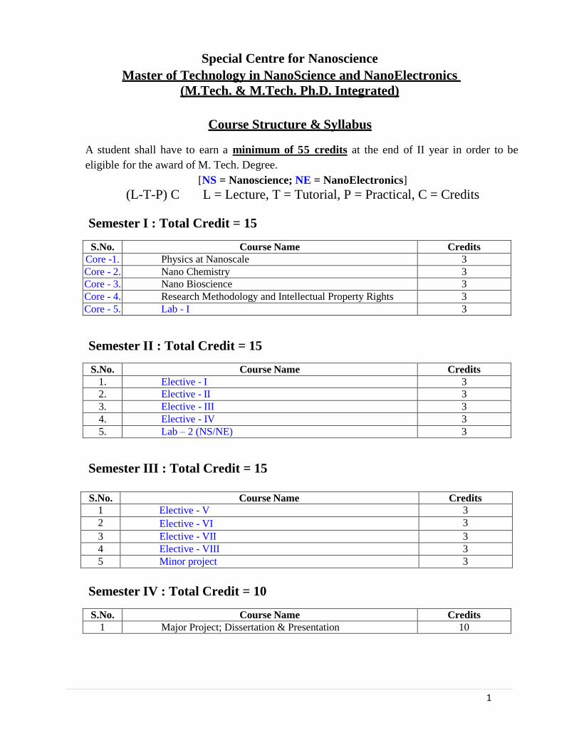
A student shall have to earn a minimum of 55 credits at the end of II year in order to be
eligible for the award of M. Tech. Degree.
[NS = Nanoscience; NE = NanoElectronics]
(L-T-P) C L = Lecture, T = Tutorial, P = Practical, C = Credits
Semester I : Total Credit = 15
S.No. Course Name Credits
Core -1. Physics at Nanoscale 3
Core - 2. Nano Chemistry 3
Core - 3. Nano Bioscience 3
Core - 4. Research Methodology and Intellectual Property Rights 3
Core - 5. Lab - I 3
Semester II : Total Credit = 15
S.No. Course Name Credits
1. Elective - I 3
2. Elective - II 3
3. Elective - III 3
4. Elective - IV 3
5. Lab – 2 (NS/NE) 3
Semester III : Total Credit = 15
S.No. Course Name Credits
1 Elective - V 3
2 Elective - VI 3
3 Elective - VII 3
4 Elective - VIII 3
5 Minor project 3
Semester IV : Total Credit = 10
S.No. Course Name Credits
1 Major Project; Dissertation & Presentation 10
2
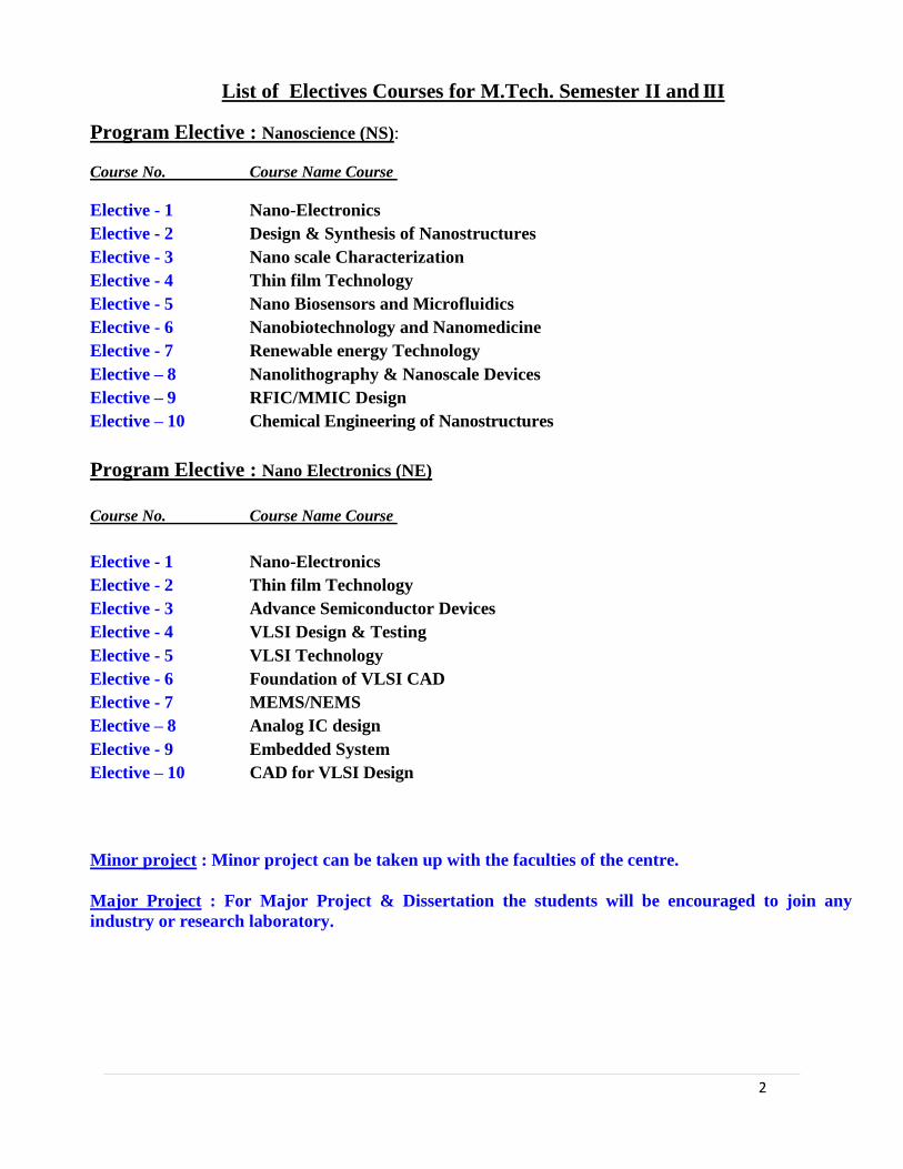
List of Electives Courses for M.Tech. Semester II and III
Program Elective : Nanoscience (NS):
Course No. Course Name Course
Elective - 1 Nano-Electronics
Elective - 2 Design & Synthesis of Nanostructures
Elective - 3 Nano scale Characterization
Elective - 4 Thin film Technology
Elective - 5 Nano Biosensors and Microfluidics
Elective - 6 Nanobiotechnology and Nanomedicine
Elective - 7 Renewable energy Technology
Elective – 8 Nanolithography & Nanoscale Devices
Elective – 9 RFIC/MMIC Design
Elective – 10 Chemical Engineering of Nanostructures
Program Elective : Nano Electronics (NE)
Course No. Course Name Course
Elective - 1 Nano-Electronics
Elective - 2 Thin film Technology
Elective - 3 Advance Semiconductor Devices
Elective - 4 VLSI Design & Testing
Elective - 5 VLSI Technology
Elective - 6 Foundation of VLSI CAD
Elective - 7 MEMS/NEMS
Elective – 8 Analog IC design
Elective - 9 Embedded System
Elective – 10 CAD for VLSI Design
Minor project : Minor project can be taken up with the faculties of the centre.
Major Project : For Major Project & Dissertation the students will be encouraged to join any
industry or research laboratory.
3
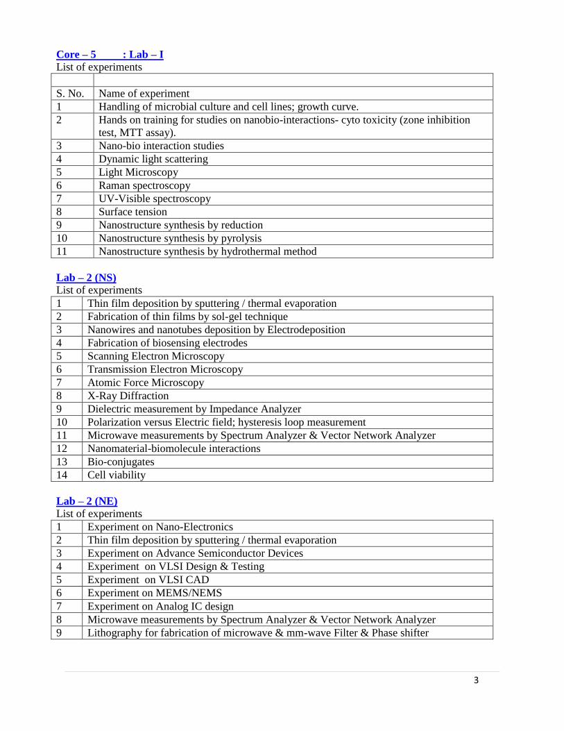
Core – 5 : Lab – I
List of experiments
S. No. Name of experiment
1 Handling of microbial culture and cell lines; growth curve.
2 Hands on training for studies on nanobio-interactions- cyto toxicity (zone inhibition
test, MTT assay).
3 Nano-bio interaction studies
4 Dynamic light scattering
5 Light Microscopy
6 Raman spectroscopy
7 UV-Visible spectroscopy
8 Surface tension
9 Nanostructure synthesis by reduction
10 Nanostructure synthesis by pyrolysis
11 Nanostructure synthesis by hydrothermal method
Lab – 2 (NS)
List of experiments
1 Thin film deposition by sputtering / thermal evaporation
2 Fabrication of thin films by sol-gel technique
3 Nanowires and nanotubes deposition by Electrodeposition
4 Fabrication of biosensing electrodes
5 Scanning Electron Microscopy
6 Transmission Electron Microscopy
7 Atomic Force Microscopy
8 X-Ray Diffraction
9 Dielectric measurement by Impedance Analyzer
10 Polarization versus Electric field; hysteresis loop measurement
11 Microwave measurements by Spectrum Analyzer & Vector Network Analyzer
12 Nanomaterial-biomolecule interactions
13 Bio-conjugates
14 Cell viability
Lab – 2 (NE)
List of experiments
1 Experiment on Nano-Electronics
2 Thin film deposition by sputtering / thermal evaporation
3 Experiment on Advance Semiconductor Devices
4 Experiment on VLSI Design & Testing
5 Experiment on VLSI CAD
6 Experiment on MEMS/NEMS
7 Experiment on Analog IC design
8 Microwave measurements by Spectrum Analyzer & Vector Network Analyzer
9 Lithography for fabrication of microwave & mm-wave Filter & Phase shifter
4
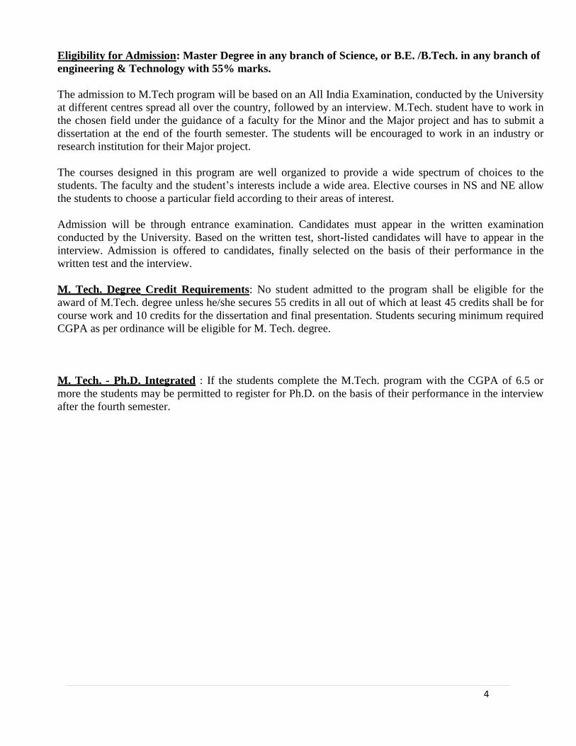
Eligibility for Admission: Master Degree in any branch of Science, or B.E. /B.Tech. in any branch of
engineering & Technology with 55% marks.
The admission to M.Tech program will be based on an All India Examination, conducted by the University
at different centres spread all over the country, followed by an interview. M.Tech. student have to work in
the chosen field under the guidance of a faculty for the Minor and the Major project and has to submit a
dissertation at the end of the fourth semester. The students will be encouraged to work in an industry or
research institution for their Major project.
The courses designed in this program are well organized to provide a wide spectrum of choices to the
students. The faculty and the student‟s interests include a wide area. Elective courses in NS and NE allow
the students to choose a particular field according to their areas of interest.
Admission will be through entrance examination. Candidates must appear in the written examination
conducted by the University. Based on the written test, short-listed candidates will have to appear in the
interview. Admission is offered to candidates, finally selected on the basis of their performance in the
written test and the interview.
M. Tech. Degree Credit Requirements: No student admitted to the program shall be eligible for the
award of M.Tech. degree unless he/she secures 55 credits in all out of which at least 45 credits shall be for
course work and 10 credits for the dissertation and final presentation. Students securing minimum required
CGPA as per ordinance will be eligible for M. Tech. degree.
M. Tech. - Ph.D. Integrated : If the students complete the M.Tech. program with the CGPA of 6.5 or
more the students may be permitted to register for Ph.D. on the basis of their performance in the interview
after the fourth semester.
5
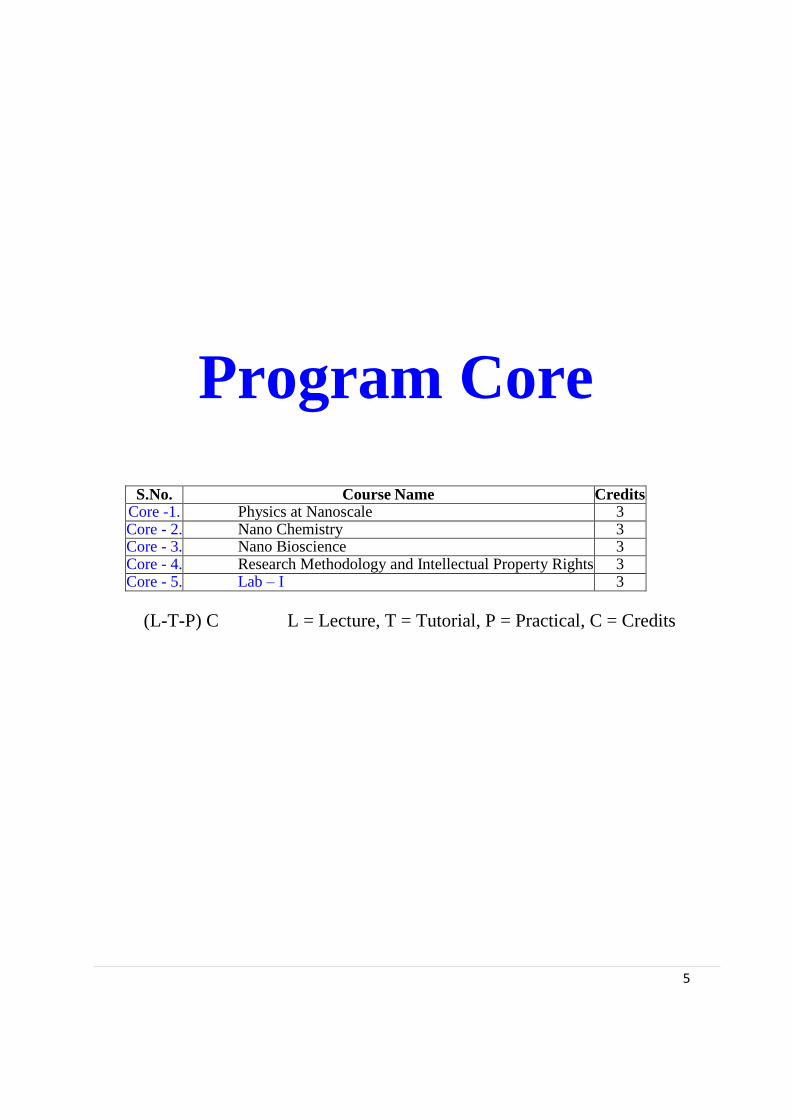
Program Core
S.No. Course Name Credits
Core -1. Physics at Nanoscale 3 Core - 2. Nano Chemistry 3 Core - 3. Nano Bioscience 3 Core - 4. Research Methodology and Intellectual Property Rights 3 Core - 5. Lab – I 3
(L-T-P) C L = Lecture, T = Tutorial, P = Practical, C = Credits
6
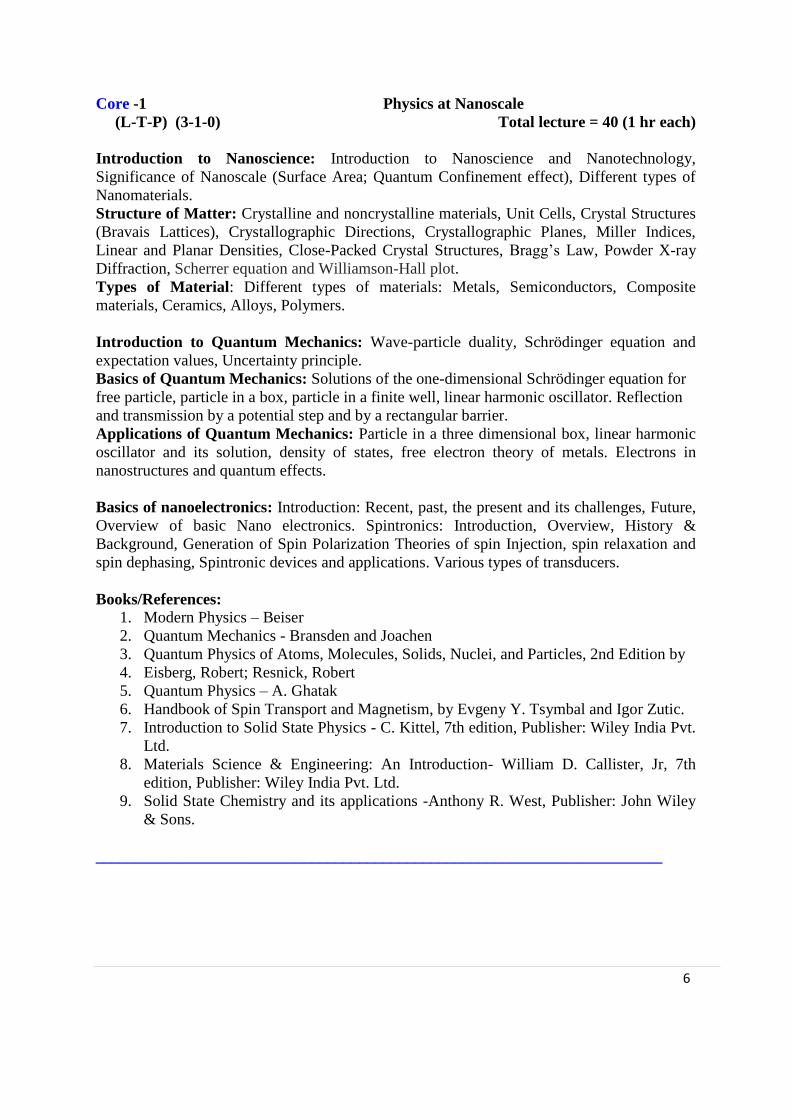
Core -1 Physics at Nanoscale
(L-T-P) (3-1-0) Total lecture = 40 (1 hr each)
Introduction to Nanoscience: Introduction to Nanoscience and Nanotechnology,
Significance of Nanoscale (Surface Area; Quantum Confinement effect), Different types of
Nanomaterials.
Structure of Matter: Crystalline and noncrystalline materials, Unit Cells, Crystal Structures
(Bravais Lattices), Crystallographic Directions, Crystallographic Planes, Miller Indices,
Linear and Planar Densities, Close-Packed Crystal Structures, Bragg‟s Law, Powder X-ray
Diffraction, Scherrer equation and Williamson-Hall plot.
Types of Material: Different types of materials: Metals, Semiconductors, Composite
materials, Ceramics, Alloys, Polymers.
Introduction to Quantum Mechanics: Wave-particle duality, Schrödinger equation and
expectation values, Uncertainty principle.
Basics of Quantum Mechanics: Solutions of the one-dimensional Schrödinger equation for
free particle, particle in a box, particle in a finite well, linear harmonic oscillator. Reflection
and transmission by a potential step and by a rectangular barrier.
Applications of Quantum Mechanics: Particle in a three dimensional box, linear harmonic
oscillator and its solution, density of states, free electron theory of metals. Electrons in
nanostructures and quantum effects.
Basics of nanoelectronics: Introduction: Recent, past, the present and its challenges, Future,
Overview of basic Nano electronics. Spintronics: Introduction, Overview, History &
Background, Generation of Spin Polarization Theories of spin Injection, spin relaxation and
spin dephasing, Spintronic devices and applications. Various types of transducers.
Books/References: 1. Modern Physics – Beiser
2. Quantum Mechanics - Bransden and Joachen
3. Quantum Physics of Atoms, Molecules, Solids, Nuclei, and Particles, 2nd Edition by
4. Eisberg, Robert; Resnick, Robert
5. Quantum Physics – A. Ghatak
6. Handbook of Spin Transport and Magnetism, by Evgeny Y. Tsymbal and Igor Zutic.
7. Introduction to Solid State Physics - C. Kittel, 7th edition, Publisher: Wiley India Pvt.
Ltd.
8. Materials Science & Engineering: An Introduction- William D. Callister, Jr, 7th
edition, Publisher: Wiley India Pvt. Ltd.
9. Solid State Chemistry and its applications -Anthony R. West, Publisher: John Wiley
& Sons.
_______________________________________________________________________
7
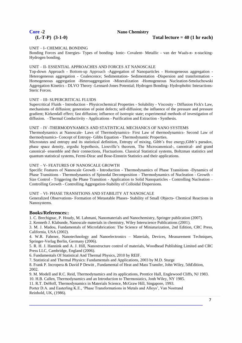
Core -2 Nano Chemistry
(L-T-P) (3-1-0) Total lecture = 40 (1 hr each)
UNIT – I- CHEMICAL BONDING
Bonding Forces and Energies- Types of bonding- Ionic- Covalent- Metallic - van der Waals-π- π-stacking-
Hydrogen bonding.
UNIT – II- ESSENTIAL APPROACHES AND FORCES AT NANOSCALE
Top-down Approach - Bottom-up Approach -Aggregation of Nanoparticles - Homogeneous aggregation -
Heterogeneous aggregation - Coalescence; Sedimentation- Sedimentation -Dispersion and transformation -
Homogeneous aggregation -Heteroaggregation -Mineralization -Homogeneous Nucleation-Smoluchowski
Aggregation Kinetics - DLVO Theory -Lennard-Jones Potential; Hydrogen Bonding- Hydrophobic Interactions-
Steric Forces.
UNIT – III- SUPERCRITICAL FLUIDS
Supercritical Fluids - Introduction - Physicochemical Properties - Solubility - Viscosity - Diffusion Fick's Law,
mechanisms of diffusion; generation of point defects; self-diffusion; the influence of the pressure and pressure
gradient; Kirkendall effect; fast diffusion; influence of isotropic state; experimental methods of investigation of
diffusion. –Thermal Conductivity - Applications - Purification and Extraction - Synthesis.
UNIT – IV -THERMODYNAMICS AND STATISTICAL MECHANICS OF NANO SYSTEMS
Thermodynamics at Nanoscale- Laws of Thermodynamics- First Law of thermodynamics- Second Law of
thermodynamics- Concept of Entropy- Gibbs Equation - Thermodynamic Properties.
Microstates and entropy and its statistical definition, Entropy of mixing, Gibb‟s free energy,Gibb‟s paradox,
phase space density, ergodic hypothesis, Liouville‟s theorem, The Microcanonical-, canonical- and grand
canonical- ensemble and their connections, Fluctuations. Classical Statistical systems, Boltzman statistics and
quantum statistical systems, Fermi-Dirac and Bose-Einstein Statistics and their applications.
UNIT – V- FEATURES OF NANOSCALE GROWTH
Specific Features of Nanoscale Growth - Introduction - Thermodynamics of Phase Transitions -Dynamics of
Phase Transitions - Thermodynamics of Spinodal Decomposition - Thermodynamics of Nucleation - Growth –
Size Control - Triggering the Phase Transition - Application to Solid Nanoparticles - Controlling Nucleation –
Controlling Growth - Controlling Aggregation-Stability of Colloidal Dispersions.
UNIT – VI- PHASE TRANSITIONS AND STABILITY AT NANOSCALE
Generalized Observations- Formation of Metastable Phases- Stability of Small Objects- Chemical Reactions in
Nanosystems.
Books/References:: 1. C. Brechignac, P. Houdy, M. Lahmani, Nanomaterials and Nanochemistry, Springer publication (2007).
2. Kenneth J. Klabunde, Nanoscale materials in chemistry, Wiley Interscience Publications (2001).
3. M. J. Madou, Fundamentals of Microfabrication: The Science of Miniaturization, 2nd Edition, CRC Press,
California, USA (2002).
4. W.R. Fahrner, Nanotechnology and Nanoelectronics – Materials, Devices, Measurement Techniques,
Springer-Verlag Berlin, Germany (2006).
5. R. H. J. Hannink and A. J. Hill, Nanostructure control of materials, Woodhead Publishing Limited and CRC
Press LLC, Cambridge, England (2006).
6. Fundamentals Of Statistical And Thermal Physics, 2010 by REIF.
7. Statistical and Thermal Physics: Fundamentals and Applications, 2003 by M.D. Sturge
8. Frank P. Incropera & David P Dewitt , Fundamental of Heat and Mass Transfer, John Wiley, 5thEdition,
2002.
9. M. Modell and R.C. Reid, Thermodynamics and its applications, Prentice Hall, Englewood Cliffs, NJ 1983.
10. H.B. Callen, Thermodynamics and an Introduction to Thermostatics, Jonh Wiley, NY 1985.
11. R.T. DeHoff, Thermodynamics in Materials Science, McGraw Hill, Singapore, 1993.
Porter D.A. and Easterling K.E., „Phase Transformations in Metals and Alloys‟, Van Nostrand
Reinhold, UK, (1986).
_______________________________________________________________________
8
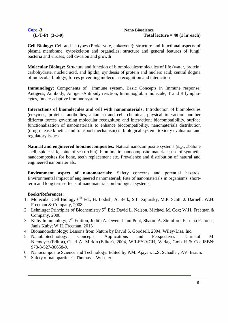
Core -3 Nano Bioscience
(L-T-P) (3-1-0) Total lecture = 40 (1 hr each)
Cell Biology: Cell and its types (Prokaryote, eukaryote); structure and functional aspects of
plasma membrane, cytoskeleton and organelles; structure and general features of fungi,
bacteria and viruses; cell division and growth
Molecular Biology: Structure and function of biomolecules/molecules of life (water, protein,
carbohydrate, nucleic acid, and lipids); synthesis of protein and nucleic acid; central dogma
of molecular biology; forces governing molecular recognition and interaction
Immunology: Components of Immune system, Basic Concepts in Immune response,
Antigens, Antibody, Antigen-Antibody reaction, Immunoglobin molecule, T and B lympho-
cytes, Innate-adaptive immune system
Interactions of biomolecules and cell with nanomaterials: Introduction of biomolecules
(enzymes, proteins, antibodies, aptamer) and cell, chemical, physical interaction another
different forces governing molecular recognition and interaction; biocompatibility, surface
functionalization of nanomaterials to enhance biocompatibility, nanomaterials distribution
(drug release kinetics and transport mechanism) in biological system, toxicity evaluation and
regulatory issues.
Natural and engineered bionanocomposites: Natural nanocomposite systems (e.g., abalone
shell, spider silk, spine of sea urchin); biomimetic nanocomposite materials; use of synthetic
nanocomposites for bone, teeth replacement etc. Prevalence and distribution of natural and
engineered nanomaterials.
Environment aspect of nanomaterials: Safety concerns and potential hazards;
Environmental impact of engineered nanomaterial; Fate of nanomaterials in organisms; short-
term and long term-effects of nanomaterials on biological systems.
Books/References:
1. Molecular Cell Biology 6th
Ed.; H. Lodish, A. Berk, S.L. Zipursky, M.P. Scott, J. Darnell; W.H.
Freeman & Company, 2008.
2. Lehninger Principles of Biochemistry 5th
Ed.; David L. Nelson, Michael M. Cox; W.H. Freeman &
Company, 2008.
3. Kuby Immunology, 7th
Edition, Judith A. Owen, Jenni Punt, Sharon A. Stranford, Patricia P. Jones,
Janis Kuby; W.H. Freeman, 2013
4. Bionanotechnology: Lessons from Nature by David S. Goodsell, 2004, Wiley-Liss, Inc.
5. Nanobiotechnology: Concepts, Applications and Perspectives- Christof M.
Niemeyer (Editor), Chad A. Mirkin (Editor), 2004, WILEY-VCH, Verlag Gmb H & Co. ISBN:
978-3-527-30658-9.
6. Nanocomposite Science and Technology. Edited by P.M. Ajayan, L.S. Schadler, P.V. Braun.
7. Safety of nanoparticles: Thomas J. Webster.
_______________________________________________________________________
9
Core -4 Research Methodology and Intellectual Property Rights
(L-T-P) (3-1-0) Total lecture = 40 (1 hr each)
Introduction to Research Methodology :
The aim of Research Methodology is to provide a background to learn how research is being done
and to put that knowledge into practice, draw conclusions from a dataset obtained through a research
question using theoretical concepts, experimental techniques and statistical evaluations.
i) Literature Survey: To provide the basis to acquaint with state of the art modalities in the
chosen field of research through textbooks and/or research articles. How to search relevant literature
and manage the references.
ii) Role of Creativity and innovations, Development of critical thinking, art of reading and
comprehending research articles.
iii) Research planning: a) Problem design and understanding the objectives of research question
and b) Hypothesis and experimental designing.
iv) Quantitative and qualitative data generation and validation: a) Ability to judge the reliability
and validity of experiments, b) Ability to perform the exploratory data analysis and data
interpretation with statistical relevance using t-test, ANOVA, c) Capability to argue the validity of
results obtained and draw a conclusion.
v) Oral communication skills, effective writing, effective research presentation, laboratory
safety issues, scientific ethics and social responsibilities
vi) Effective scientific proposal, Review article and Research paper writing, Technical report and
Thesis writing.
Introduction to Research Methods in Nanoscience (from view of Physics, chemistry, biological
and environmental sciences)
Experimental Research: Design of experiments, Data evaluation. Documentation.
Tips for efficient scientific writing: Identifying highlights. Structure of document.
Advantages of structuring. Avoiding repetition.
Ethical Issues & IPR:
Plagiarism, ethical issues, chemical and biological waste handling and disposal, Patenting
information etc.
10
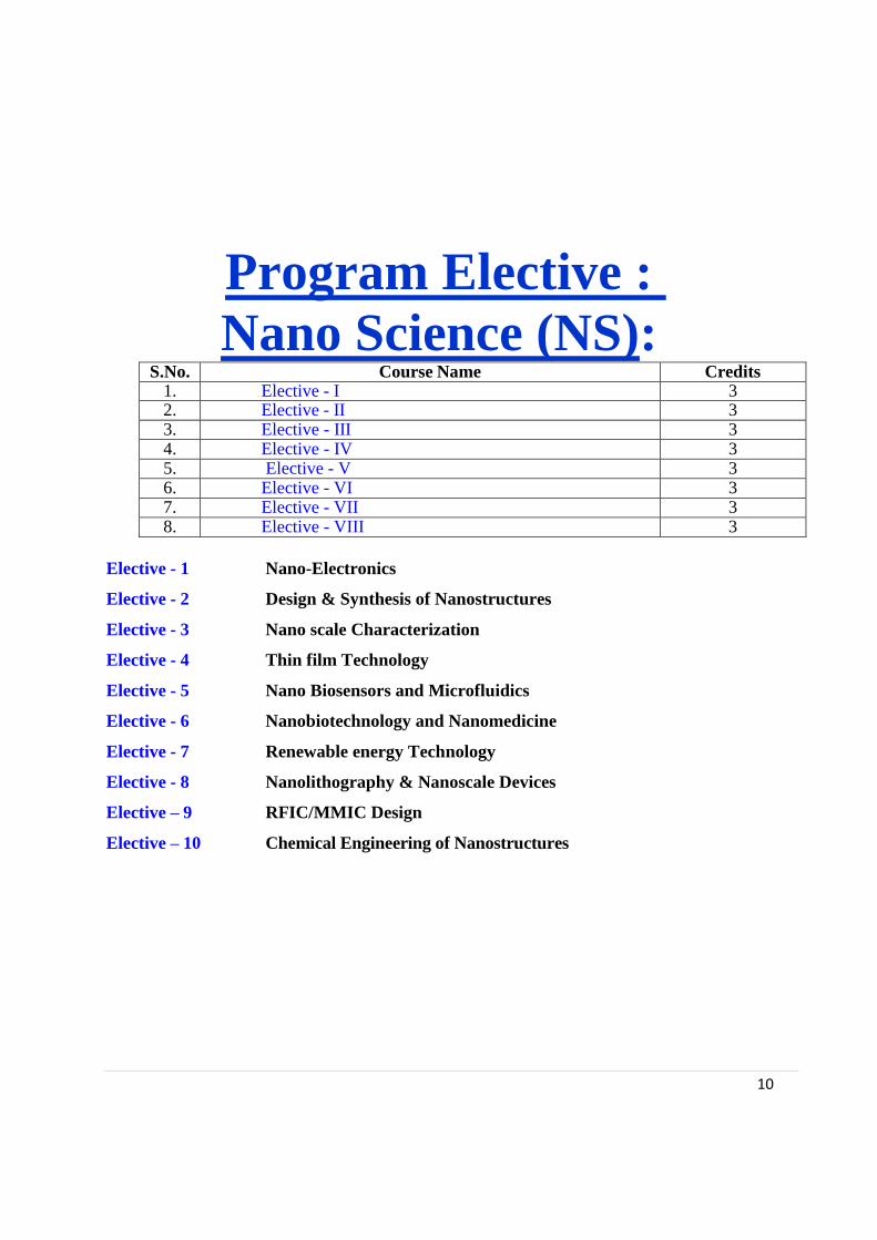
Program Elective :
Nano Science (NS): S.No. Course Name Credits
1. Elective - I 3 2. Elective - II 3 3. Elective - III 3 4. Elective - IV 3 5. Elective - V 3 6. Elective - VI 3 7. Elective - VII 3 8. Elective - VIII 3
Elective - 1 Nano-Electronics
Elective - 2 Design & Synthesis of Nanostructures
Elective - 3 Nano scale Characterization
Elective - 4 Thin film Technology
Elective - 5 Nano Biosensors and Microfluidics
Elective - 6 Nanobiotechnology and Nanomedicine
Elective - 7 Renewable energy Technology
Elective - 8 Nanolithography & Nanoscale Devices
Elective – 9 RFIC/MMIC Design
Elective – 10 Chemical Engineering of Nanostructures
11
Elective - 1 : Nano-Electronics
(L-T-P) (3-1-0) Total lecture = 40 (1 hr each)
QUANTUM DEVICES
Charge and spin in single quantum dots- Coulomb blockade– Electrons in mesoscopic
structures - single electron transfer devices (SETs) – Electron spin transistor – resonant
tunnel diodes, tunnel Field Effect Transistors (FET)- quantum interference transistors
(QUITs) - quantum bits (qubits).
NANOELECTRONIC DEVICES
Electronic transport in 1, 2 and 3 dimensions- Quantum confinement - energy sub-bands -
Effective mass –Drude conduction - mean free path in 3D - ballistic conduction - phase
coherence length - quantized conductance -Buttiker-Landauer formula- electron transport in
pn junctions - short channel Nano Transistor –Metal Oxide Semiconductor (MOS)FETs -
Advanced MOSFETs - Trigate FETs, Fin-FETs - CMOS.
MOLECULAR NANOELECTRONICS
Electronic and optoelectronic properties of molecular materials - Electrodes & contacts –
functions – molecular electronic devices - elementary circuits using organic molecules-
Organic materials based rectifying diode switches– TFTs- OLEDs- OTFTs – logic switches.
SPINTRONICS
Spin tunneling devices - Magnetic tunnel junctions- Tunneling spin polarization - Giant
tunneling using MgO tunnel barriers - Tunnel-based spin injectors - Spin injection and spin
transport in hybrid nanostructures - spin filters –spin-diodes - Magnetic tunnel transistor -
Memory devices and sensors - ferroelectric random access memory (RAM)- Magnetic-
RAMS-Field Sensors - Multiferro electric sensors- Spintronic Biosensors.
Books/References:
1. V. Mitin, V. Kochelap, M. Stroscio, ―Introduction to Nanoelectronics, Cambridge
University Press (2008).
2. Rainer Waser, ―Nanoelectronics and Information Technology: Advanced Electronic
Materials and NovelDevices, Wiley-VCH (2003).
3. Karl Goser, Peter Glosekotter, Jan Dienstuhl, ―Nanoelectronics and Nanosystems,
Springer (2004).
4. SadamichiMaekawa, ―Concepts in Spin Electronics, Oxford University Press (2006).
5. L. Banyai and S.W.Koch, ―Semiconductor Quantum Dots, World Scientific (1993).
6. Edward L. Wolf, ―Nanophysics and Nanotechnology: An Introduction to Modern
Concepts in Nanoscience,Wiley-VCH (2006).
_______________________________________________________________________
12
Elective - 2 Design & Synthesis of Nanostructures
(L-T-P) (3-1-0) Total lecture = 40 (1 hr each)
Physical Methods: Inert gas condensation, Arc discharge, RF-plasma, Plasma arc technique,
Ion sputtering, Laser ablation, Laser pyrolysis, Ball Milling, Molecular beam epitaxy,
Chemical vapour deposition method and other variants, electrodeposition. Microwave
synthesis of NPs.
Chemical Methods:Metal nanocrystals by reduction, Solvothermal synthesis, Photochemical
synthesis, Nanocrystals of semiconductors and other materials by arrested precipitation,
Thermolysis routes, Sonochemical routes, Liquid-liquid interface, Hybrid methods, Solvated
metal atom dispersion, Post-synthetic size-selective processing. Solgel, Micelles and
microemulsions, Cluster compounds.
Biological Methods of Synthesis: Use of bacteria, fungi, Actinomycetes for nanoparticle
synthesis, Magnetotactic bacteria for natural synthesis of magnetic nanoparticles; Mechanism
of formation; Viruses as components for the formation of nanostructured materials;
Biological material based metallic nanowires, Synthesis process and application. Electro-
spinning Synthesis of Nanofibres, Microfluidic Synthesis of NPs, Green Synthesis of NPs.
Books/References:
1). Introduction to Nanotechnology - Charles P. Poole Jr. and Franks. J. Qwens, Publisher:
Wiley
2). Nanomaterials Handbook- Yury Gogotsi, Publisher: Taylor & Francis
3). Processing & properties of structural naonmaterials by Leon L. Shaw (editor), Publisher:
Wiley
4). Chemistry of nanomaterials : Synthesis, properties and applications by CNR Rao et.al.
Publisher: Wiley
5). Semiconductor Nanowires: Materials, Synthesis, Characterization and Applications
(Woodhead Publishing Series in Kindle Edition(2015) by Arbiol, J and Xiong, Q.
6). Novel Synthesis and Characterization of Nanostructured Materials (Engineering
Materials)(2013) by Annelise Alves and Carlos P. Bergmann.
7). Handbook of Nanoscience, Engineering, and Technology (Electrical Engineering
Handbook)2002 by William A. Goddard III and Donald Brenner.
8). The Power of Click Chemistry for Molecular Machines and Surface Patterning (Springer
Theses 2011) by Jason M. Spruell.
_______________________________________________________________________
13
Elective - 3 Nano scale Characterization
(L-T-P) (3-1-0) Total lecture = 40 (1 hr each)
Characterizations using Scattering and Imaging techniques :
X-Ray Diffraction. Dynamic light scattering, Light Microscopy, Scanning Electron
Microscopy based techniques (Secondary electron imaging, backscattered electron imaging,
Electron backscattered diffraction (EBSD)). TEM based techniques (diffraction contrast
imaging, Electron diffraction, High resolution imaging). Scanning probe microscopies
(Atomic Force Microscopy, Piezeo Force Microscopy, Scanning Tunneling Microscopy).
Characterization using Spectroscopic techniques :
Ultraviolet-Visible-Infrared, Fourier Transform Infrared Spectroscopy. Raman. X-ray
Photoelectron Spectroscopy. Photoluminescence. Fluorescence. Phosphorescence.
Electroluminescence. Photoconductivity. Auger spectroscopy. Energy Dispersive X-ray
Spectroscopy, Wavelength Dispersive X-ray Spectroscopy, Electron Energy Loss
Spectroscopy, Scanning tunneling spectroscopy. Differential Thermal analysis (DTA) -
Differential Scanning Calorimetry (DSC) – Thermo-gravimetric analysis (TGA)
Electrical measurement techniques : Resistivity, Polarization, Dielectric properties, Electrochemical techniques (Cyclic
voltametry).
Magnetic measurement techniques :
Magneto-Resistance, Vibrating Sample Magnetometer, Superconducing Quantum
Interference Device, Magneto Optical Kerr Effect.
Books/References:
1. Nanostructures and Nanomaterials : Synthesis, Properties, and Applications, 2nd
Ed., G
Cao, Z Wang, World scientific, 2011
2. Chemistry of nanomaterials : Synthesis, properties and applications, CNR Rao, A
Mueller, A K Cheetham, Wiley, 2004.
3. Nanocrystals: Synthesis, properties and applications, CNR Rao, P J Thomas, G U
Kulkarni, Springer, 2007.
4. Elements of X-Ray Diffraction, 3rd
Ed., B D Cullity, R W Stock, Pearson, 2014.
5. Scanning Microscopy for Nanotechnology, W. Zhou, Z. L. Wang (editors), Springer,
2006
6. Electron Microscopy and Analysis (3rd
Ed.), Goodhew P J, Humphreys J, Beanland R,
Taylor & Francis, 2000
7. Transmission Electron Microscopy: A Textbook for Materials Science (4-Vol Set)-David
B. Williams and C. Barry Carter, Springer, 2009
8. Dynamic Light Scattering: With Applications to Chemistry, Biology, and Physics, Bruce
J. Berne, Robert Pecora, Courier Dover Publications, 2000
_______________________________________________________________________
14
Elective - 4 Thin film Technology
(L-T-P) (3-1-0) Total lecture = 40 (1 hr each)
THIN FILM DEPOSITION TECHNIQUES
Introduction –Kinetic theory of gases - Physical vapour deposition techniques – Physics and
Chemistry of Evaporation - Thermal evaporation – Pulsed laser deposition – Molecular beam
epitaxy – Sputtering deposition –Direct Current, Radio Frequency, Magnetron, Ion beam and
reactive sputtering - Chemical methods – Thermal Chemcial Vapour Deposition – Plasma
enhanced Chemcial Vapour Deposition – Spray Pyrolysis – Sol Gel method – Spin and Dip
coating – Electrophoretic and electrochemical deposition. Self -assembled monolayers.
NUCLEATION, GROWTH AND EPITAXY
Substrate surface, Adsorption, Surface energy, film growth modes, nucleation model,
manifestations of epitaxy, lattice misfit and defect formation, morphology, grain growth,
texture, microstructure control.
DIFFUSION, REACTIONS, TRANSFOMATIONS AND STRESS
Fundamentals of diffusion –Grain Boundary Diffusion, metal-semiconductor reactions,
phase transformations-Origin of Thin film stress - Classifications of stress – Stress in
epitaxial films – Growth Stress in polycrystalline films – Correlation between film stress and
grain structure – Mechanisms of stress evolution – film stress and substrate curvature –
Stoney formula – Methods of curvature measurement – Scanning laser method
CHARACTERIZATION TECHNIQUES
Glancing angle XRD. Auger Electron spectroscopy – Photoelectron Spectroscopy –
Secondary Ion Mass Spectroscopy –Rutherford Backscattering spectroscopy - Ellipsometry –
Profilometry, Low Energy Electron Diffraction – Reflection High Energy Electron
Diffraction. Scanning Electron Microscopy, Transmission Electron Microsc opy, Atomic
Force Microscopy and Energy Dispersive X-ray analysis of thin films.
Books/References:
1. Amy E. Wendt, Thin Films - High density Plasmas, Volume 27, Springer Publishers.
(2006).
2. Rointan F. Bunshah, Hand Book of Deposition technologies for Thin Films and coatings
by Science, Technologyand Applications ,Second Edition , Noyes Publications, (1993).
3. Milton Ohring, Materials Science of Thin films Published by Academic Press
Limited(1991)
4. L.B. Freund and S.Suresh, Thin Film Materials, (2003).
5. Hans Luth, Solid surfaces, Interfaces and Thin Films‟ 4th edition, Springer Publishers
(2010).
6. HaraldIbach, Physics of Surfaces and Interfaces, Springer Publishers (2006).
7. . Thin Film Phenomena, K. L. Chopra, Mc Graw-Hill Book Company (1969)
_______________________________________________________________________
15
Elective - 5 Nano Biosensors and Microfluidics
(L-T-P) (3-1-0) Total lecture = 40 (1 hr each)
Basic of Biosensor: Introduction and various components of biosensors. Types of biosensors,
advantages and limitations, biocatalysis and bio-affinity based biosensors & microorganisms
based biosensors, biologically active material and analytes, nanomaterials- biomolecule
hybrids as sensing surface. Applications of biosensors for clinical diagnosis and
environmental monitoring.
Transducers in Biosensors: Transducers principles, calorimetric, optical, electrochemical
(potentiometric/amperometric conductor metric/ resistormetric or impedimetric),
piezoelectric, surface plasmon resonance, evanescent waves based biosensors etc.
Nanomaterials based electrochemical biosensors: Fabrication of nanomaterials based
biosensors, nanobiochips or bimolecular electronics and their application in modern sciences.
Non-invasive biosensors for clinical analysis. Application of nanobiosensors to
environmental samples
Fabrication of electrochemical microfluidic devices: Introduction of microfluidic devices,
Design of mask or patterned electrode and channels and its applications, Basics of
microfluidics and fluid dynamics Microfluidic devices: microchannels, microvalves,
micropumps, microneedles, micro-reservoirs, micro-reactors, nanomaterials in microfluidics.
Lab-on–a-chip for multianalytes detection of clinical and environmental samples.
Microfabricated sensors and the commercial development of the I- stat Point-of-Care system.
Nanomaterials based Optical biosensors: General principles of optical sensing, photo
detectors, optical fiber sensors and indicator mediated transducers. Detection of absorbance,
reflectance, and fluorescence etc. Fabrication of Fluorescence Resonance Energy Transfer
based biosensor. Chemiluminescence - based biosensors for clinical and environmental
samples.
Books/References:
1. D. L. Wise; Applied Bio Sensors“, Butterworth, London
2. Biomedical Nanotechnology; Neelina Malsch.
3. Jun Li and Nianqiang Wu; Biosensors Based on Nanomaterials and Nanodevices
(Nanomaterials and their Applications)
4. Chandran Karunakaran; Biosensors and Bioelectronics
5. Eric Lagally; Microfluidic and Nanotechnology: biosensing to the single molecular
limit (Devices, circuit and system) 2014.
6. Lab-on-a-Chip Technology (Vol. 1): Fabrication and Microfluidics
_______________________________________________________________________
16
Elective - 6 Nanobiotechnology and Nanomedicine
(L-T-P) (3-1-0) Total lecture = 40 (1 hr each)
Introduction to nanobiotechnology and nanostructures: Nanotechnology and its interface
with biology, Biomedical applications of nanotechnology, Nano-pharmaceutical materials,
Therapeutic potential of nanomaterials, Drug delivery and Controlled release,
Nanomicrobicidals, Diseased tissue destruction using Nanoparticles, Molecular nanoprobes/
nanolabels, Tissue engineering (cell biological fundamentals of tissue engineering and
applications of nanosciences in regenerative medicine), Environmental Toxicity evaluation of
nanomaterials using microorganisms, Nanotechnology in food and environment.
Nanomedicine: Introduction, Drug design, Drug loading onto nanoparticles and in vitro
release, Nano-bio interactions and associated cellular and molecular changes, Enhanced
permeability and retention (EPR) effect, Evasion of host immune system, Stimulating the
immune system, Escaping the endosomes inside the cells, Pharmacology (Transmembrane
Signaling, Efficacy of nano based drug, Toxicology of nano based drug, Pharmacokinetics
and Pharmacodynamics, Drug metabolism).
Nanomedicine in infectious and chronic diseases:
Infectious Diseases: Introduction to infectious diseases, Existing and emerging Microbial
Pathogens (Bacterial, fungal and viral), Disease Biomarkers, Biofilms, Multi Drug resistance
(MDR), Failure of drug therapy, Nanodrugs for MDR.
Chronic Diseases: Introduction to chronic diseases (e.g. Cancer, Diabetes, Neurological
disorders), Etiology of Cancer, Disease Biomarkers, Existing Therapies and Constraints,
Nanomedicine for chronic diseases. Pros and cons of nanotechnology in the clinics.
Books/References:
Bionanotechnology: Lessons from Nature by David S. Goodsell, 2004, Wiley-Liss, Inc.
Nanobiotechnology: Concepts, Applications and Perspectives- Christof M.
Niemeyer (Editor), Chad A. Mirkin (Editor), 2004, WILEY-VCH, Verlag Gmb H & Co. ISBN:
978-3-527-30658-9.
Nanobiotechnology - II more concepts and applications. (2007) - Chad A Mirkin and Christof M.
Niemeyer (Eds), Wiley VCH.
Principles of Tissue Engineering - Robert Lanza, Robert Langer, and Joseph P.
Nanomedicine, Volume I: Basic Capabilities. Robert A. Freitas Jr., Landes, 1999, Bioscience.
Nanomedicine, Vol. IIA: Biocompatibility by Robert A. Freitas.
Nanotechnology in Drug Delivery. Melgardt M.deVilliers, Pornanong Aramwit, Glen S. Kwon,
2009, Springer-American Association of Pharmaceutical Scientists Press.
Basic and Clinical Pharmacology, Bertram Katzung and Anthony Trevor; Publisher: McGraw-Hill
Education.
_______________________________________________________________________
17
Elective - 7 Renewable energy Technology
(L-T-P) (3-1-0) Total lecture = 40 (1 hr each)
Solar cell module materials and assembly
PV modules: Module and Circuit Design - Identical and Non-identical Cells – Module
Structuring and assembly - Environmental Protection - Thermal Considerations – Electrical
Considerations and output conditioning - assembly materials – interconnects – crystalline and
thin film modules - issues with solar PV modules, bypass diode and blocking diode – module
testing and analysis.
Nanomaterials in Energy Storage Devices: MWNT for Li Ion Batteries, Nanomaterials in
Electrodes, Hybrid Nanotubes: Anode Material, Supercapacitor, Battery Electrodes.
Energy from waste- Bio-chemical Conversion: Anaerobic digestion of sewage and
municipal wastes, direct combustion of MSW-refuse derived solid fuel, industrial waste, agro
residues, anaerobic digestion biogas production, land fill gas generation and utilization,
present status of technologies for conversion of waste into energy, design of waste to energy
plants for cities, small townships and villages.
Characterization and analysis: Device isolation & analysis - Ideal cell under illumination
solar cell parameters short circuit current, open circuit voltage, fill factor, efficiency; optical
losses; electrical losses, surface recombination velocity, quantum efficiency - measurements
of solar cell parameters; I-V curve & L-I-V characteristics, internal Quantum yield
measurements –Effects of series and parallel resistance and Temperature - Loss analysis.
Newer Energy Materials: Carbon nano-tubes (CNTs) and multiwall carbon nanotubes
(MWCNTs), graphene, graphene oxide, reduced graphene oxide and Polymer composites -
classification, methods of production, properties, and its utility in making energy devices.
Books/References:
1) D Y Goswami, Frank Kreith and J F Kreider, Principles of Solar Engineering, Taylor &
Francis, 1998
2)Sie-Chin Tjong, Nanocrystalline Materials. Elsevier, 2014
3) K L Chopra, Suhit Ranjan Das, Thin Film Solar Cells, Springer Science, 1983
4) David Linden, Thomas B. Reddy, Handbook of batteries, 3rd Edition, Mcgraw Hill, 2002
_______________________________________________________________________
18
Elective - 8 Nanolithography & Nano-scale Devices
(L-T-P) (3-1-0) Total lecture = 40 (1 hr each)
Overview: Nano devices, Nano materials, Nano characterization.
Nanolithography : Moore‟s Laws (1,2,&3) and technology‟ Roadmap–clean rooms
Processing Methods: - Cleaning – Oxidation – Lithography – Etching- – CVD - Diffusion –
Ion implantation – metallization – state of the art CMOS architectures Photolithography
Overview – Critical Dimension – Overall Resolution – Line-Width – Lithographic Sensitivity
and Intrinsic Resist Sensitivity (Photochemical Quantum Efficiency) – Resist Profiles –
Contrast and Experimental Determination of Lithographic Sensitivity – Resolution in
Photolithography – Photolithography Resolution Enhancement Technology.
Next-Generation Technologies: – State-Of-The-Art (including principles, capabilities,
limits, applications) EUV lithography – Phase-shifting photolithography – X-ray lithography
– Electron Beam Direct Writing System –Focused ion beam (FIB) lithography – Neutral
atomic beam lithography – Plasma-Aided Nanofabrication – Soft Lithography – Nanosphere
Lithography – Nano-imprint – Dip-pen nanolithography – key consequences of adopted
techniques.
Nano-scale devices: Definition of Technology node, Basic CMOS Process flow. MOS
Scaling theory, Issues in scaling MOS transistors : Short channel effects, Description of a
typical 65 nm CMOS technology. Requirements for Non classical MOS transistor.
MOS capacitor, Role of interface quality and related process techniques, Gate oxide thickness
scaling trend, SiO2 vs High-k gate dielectrics. Integration issues of high-k .
Interface states, bulk charge, band offset, stability, reliability - Qbd high field, possible
candidates, CV and IV techniques.
Books/References:
1) Zheng Cui, Nanofabrication, Principles, Capabilities and Limits, Springer Science +
business media, NewYork (2008).
2) Huff, Howard, Into The Nano Era: Moore's Law Beyond Planar Silicon CMOS (Vol. 106),
Springer Series inMaterials Science, Springer-Verlag Berlin (2009).
3) Marc J. Madou, Fundamentals of Microfabrication: The Science of Miniaturization, 2nd
Edition, CRC Press,California, USA (2002).
4) Nanoscale Devices- Gianfranco Cerofolini, Publisher: Springer
5) Nanoscale Devices - Fundamentals and Applications by Rudolf Gross, Anatolie
Sidorenko, Lenar Tagirov, Publisher: Springer
_______________________________________________________________________
19
Elective - 9 RFIC/MMIC Design
(L-T-P) (3-1-0) Total lecture = 40 (1 hr each)
Microwave Integrated Circuits: Thick and thin film technology, Hybrid MIC‟s, Monolithic
MIC technology, Analysis of Strip line and Microstrip Line: Method of conformal
transformation, Charactetic parameters of Strip, Microstrip lines, Microstrip circuit design,
Impedance transformers, Filters, Lumped constant microstrip circuits, Coupled Microstrip
and Directional Coupler.
Microwave Measurements – Concept of vector network analyzer, Basic block diagram of
vector network analyzer (VNA), Application of vector network analyzers. Basic block
diagram of a spectrum analyzer, functions & applications of a spectrum analyzer. Time
Domain Electrometer (TDR) & IC Technology. Microwave Measurements using Vector
Network Analyzer, Spectrum Analyser, etc.
MMIC Planar circuit Design. MMIC Mixer Design and Simulation. Design of RF Power
Amplifier. Design Microwave voltage controlled oscillator (VCO). Design MMIC Mixer and
Simulation. Design Microstrip Filter. Designing mm-wave integrated filters. Design of a
Broadband MMIC Frequency Doubler.
Fabrication processes for microstrip line and co-planar wave guide geometry. In-corporation
of magnetic nanostructures like ultra-thin film, nano-wires and nano-particles into magnetic-
MMICs. Characterization & theory of magnetically tunable Monolithic microwave reciprocal
and non-reciprocal devices. Review of current research in MMICs design, fabrication and
testing.
Books/References:
1) D.Pozar,” Microwave Engineering”, 2nd Ed, John Wiley
2) T.S.Laverghetta-“ Hand book on Microwave Testing”,Artech House,1981
3) Samuel. Y. Liao,”Microwave devices and circuits”, Pearson Edn., 2003.
4) Coplanar Waveguide Circuits, Components, and Systems (Wiley Series in Microwave and
Optical Engineering), by Rainee N. Simons
_______________________________________________________________________
20
Elective – 10 Chemical Engineering of Nanostructures
(L-T-P) (3-1-0) Total lecture = 40 (1 hr each)
INTRODUCTION & BASIC CONCEPTS OF SYNTHESIS: Review of forces and interaction at Nanoscale.
METAL NANOPARTICLES: Chemical Reduction-Seed Mediated-Laser (Pulsed Laser)Ablation-
Lithography-Carbonyl decomposition-Electrochemical discharges- Green Chemistry-Ligand Free Synthesis-
Reduction Methods-Lee-Meisel Method-Creighton method- Schneider method-Water Soluble-Chitosan
Mediated Synthesis-Synthesis using tea Extract-Hydrophilic and Hydrophobic NPs-Impregnation method-
Pluronic Based Synthesis- Polyol Based Synthesis- Using thiol-functionalized ionic liquid- Polyol Based
Synthesis- Colloid Method- Reverse Micellar Synthesis- Bioreduction Synthesis- Thermal Decomposition -
Sonochemical Synthesis- Reduction by plant extracts- One Pot Synthesis- Polyol Based- Foam Based Synthesis-
Microemulsion method - Polyol Method- Solvothermal Method- Catalytic Decomposition- Templated
Synthesis- Thermolysis in organic solvent- Hot Injection Method.
METAL OXIDE NANOPARTICLES: Sol-gel Synthesis- Template Method- Sputtering Method-
Microemulsion Method- Precipitation Method- Wet Chemical Reduction Synthesis- Hydrothermal
Decomposition Method- Biosynthesis- Thermal Decomposition- Facile Method- Microwave Synthesis- Plant
Extract Method- Chemical Reduction Method- Supramolecular Method- Plant Extract Method- Precipitation
method- Hydrolysis Method-Plant Extract Method- Co-precipitation Method- Laser Ablation Method- Aqueous
Method-Laser Pyrolysis- Coprecipitation- Sonochemical Method- Microwave Synthesis- Thermolysis-
Sonochemical Method- Precipitation Method- Thermal Decomposition- Solventless Method- Microwave
Assisted- Solution-coprecipitation Method-Alkoxide-based Method-Heat Treatment- Microwave Radiation -
Stöber Method- Ultrasonication- One-pot Synthesis- Biosynthesis- Templated Synthesis- Pulse Laser Ablation
Method-Precipitation Method- Plant Extract Method- Biological Method.
LOW-DIMENSIONAL NANOCRYSTALS: Solvothermal Method- Chemical Synthesis-Thermal
Decomposition(Thermolysis) Method -Hydrothermal Method- Laser Ablation- Sonochemical Method-
Template Synthesis- Protein Mediated- Chemical Synthesis- Electrochemical Method- Hot-injection Method-
Green Synthesis- Facile Approach- Single-step Synthesis- Single Step Method- Gamma Irradiation- Chemical
Synthesis- Single Source Precursor- Facile Synthesis- Ambient condition and Single Precursor- Chemical
Method- Single Precursor Thermolysis- Other Methods.
POLYMERIC NANOPARTICLES: One-pot Synthesis- Solvent Displacement-Plant Extract Synthesis-
Electrospraying-Free-radical Polymerization-Emulsion Solvent- Nanoprecipitation- Microfluidic
nanoprecipitation)-Microemulsion Polymerization- Surfactant-free Emulsion Polymerization - Click Chemistry-
Free-radical Miniemulsion Polymerization Synthesis- Miniemulsion Co-polymerization- Interfacial
Polycondensation-Emulsion Polymerization- Phase-inversion Synthesis-Solvent Diffusion Method- Free-radical
Mircoemulsion Polymerization- Inverse Heterophase Polymerization-Reverse Micellar Synthesis-
Freezing/thawing Cycle- Nanoprecipitation.
BIOPOLYMERIC NANOPARTICLES: Carbohydrate Nanoparticles- Protein Nanoparticles-Nucleic acid
nanoparticles-Dissolution method-Complexation-Conjugation method-Micellar route-Electrospinning.
SUPRAMOLECULAR CHEMISTRY: Supramolecular Chemistry: Applications and Prospects - From
Molecular to Supramolecular Chemistry – Molecular Recognition - Anionic Coordination Chemistry and
Recognition of Anionic Substrates - Multiple Recognition Applications and Prospects.
Books/References:
1. Guozhong Cao, Nanostructures &Nanomaterials Synthesis, Properties G; Z: Applications, World Scientific
Publishing Private, Ltd., Singapore (2004).
2. C. N. Rao, A. Muller, A. K. Cheetham, Nanomaterials chemistry, Wiley-VCH (2007).
3. Encyclopedia of Nanoscience and Nanotechnology: 2003 by H.S. Nalwa.
4. Nanoscience and Nanotechnology Handbook 2010 by H. Panda. _______________________________________________________________________
21
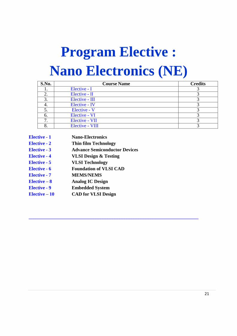
Program Elective :
Nano Electronics (NE) S.No. Course Name Credits
1. Elective - I 3 2. Elective - II 3 3. Elective - III 3 4. Elective - IV 3 5. Elective - V 3 6. Elective - VI 3 7. Elective - VII 3 8. Elective - VIII 3
Elective - 1 Nano-Electronics
Elective - 2 Thin film Technology
Elective - 3 Advance Semiconductor Devices
Elective - 4 VLSI Design & Testing
Elective - 5 VLSI Technology
Elective - 6 Foundation of VLSI CAD
Elective - 7 MEMS/NEMS
Elective – 8 Analog IC Design
Elective - 9 Embedded System
Elective – 10 CAD for VLSI Design
_______________________________________________________________________
22
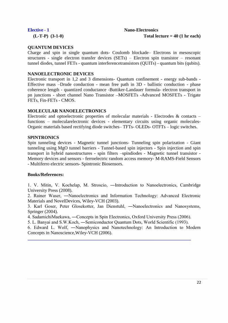
Elective - 1 Nano-Electronics
(L-T-P) (3-1-0) Total lecture = 40 (1 hr each)
QUANTUM DEVICES
Charge and spin in single quantum dots- Coulomb blockade– Electrons in mesoscopic
structures - single electron transfer devices (SETs) – Electron spin transistor – resonant
tunnel diodes, tunnel FETs - quantum interferencetransistors (QUITs) - quantum bits (qubits).
NANOELECTRONIC DEVICES
Electronic transport in 1,2 and 3 dimensions- Quantum confinement - energy sub-bands -
Effective mass –Drude conduction - mean free path in 3D - ballistic conduction - phase
coherence length - quantized conductance -Buttiker-Landauer formula- electron transport in
pn junctions - short channel Nano Transistor –MOSFETs -Advanced MOSFETs - Trigate
FETs, Fin-FETs - CMOS.
MOLECULAR NANOELECTRONICS
Electronic and optoelectronic properties of molecular materials - Electrodes & contacts –
functions – molecularelectronic devices - elementary circuits using organic molecules-
Organic materials based rectifying diode switches– TFTs- OLEDs- OTFTs – logic switches.
SPINTRONICS
Spin tunneling devices - Magnetic tunnel junctions- Tunneling spin polarization - Giant
tunneling using MgO tunnel barriers - Tunnel-based spin injectors - Spin injection and spin
transport in hybrid nanostructures - spin filters –spindiodes - Magnetic tunnel transistor -
Memory devices and sensors - ferroelectric random access memory- M-RAMS-Field Sensors
- Multiferro electric sensors- Spintronic Biosensors.
Books/References:
1. V. Mitin, V. Kochelap, M. Stroscio, ―Introduction to Nanoelectronics, Cambridge
University Press (2008).
2. Rainer Waser, ―Nanoelectronics and Information Technology: Advanced Electronic
Materials and NovelDevices, Wiley-VCH (2003).
3. Karl Goser, Peter Glosekotter, Jan Dienstuhl, ―Nanoelectronics and Nanosystems,
Springer (2004).
4. SadamichiMaekawa, ―Concepts in Spin Electronics, Oxford University Press (2006).
5. L. Banyai and S.W.Koch, ―Semiconductor Quantum Dots, World Scientific (1993).
6. Edward L. Wolf, ―Nanophysics and Nanotechnology: An Introduction to Modern
Concepts in Nanoscience,Wiley-VCH (2006).
_______________________________________________________________________

23
Elective - 2 Thin film Technology
(L-T-P) (3-1-0) Total lecture = 40 (1 hr each)
THIN FILM DEPOSITION TECHNIQUES
Introduction –Kinetic theory of gases - Physical vapour deposition techniques – Physics and
Chemistry of Evaporation - Thermal evaporation – Pulsed laser deposition – Molecular beam
epitaxy – Sputtering deposition –Direct Current, Radio Frequency, Magnetron, Ion beam and
reactive sputtering - Chemical methods – Thermal Chemcial Vapour Deposition – Plasma
enhanced Chemcial Vapour Deposition – Spray Pyrolysis – Sol Gel method – Spin and Dip
coating – Electrophoretic and electrochemical deposition. Self Assembled monolayers.
NUCLEATION, GROWTH AND EPITAXY
Substrate surface, Adsorption, Surface energy, film growth modes, nucleation model,
manifestations of epitaxy, lattice misfit and defect formation, morphology, grain growth,
texture, microstructure control.
DIFFUSION, REACTIONS, TRANSFOMATIONS AND STRESS
Fundamentals of diffusion –Grain Boundary Diffusion, metal-semiconductor reactions,
phase transformations-Origin of Thin film stress - Classifications of stress – Stress in
epitaxial films – Growth Stress in polycrystalline films – Correlation between film stress and
grain structure – Mechanisms of stress evolution – film stress and substrate curvature –
Stoney formula – Methods of curvature measurement – Scanning laser method
CHARACTERIZATION TECHNIQUES
Glancing angle XRD. Auger Electron spectroscopy – Photoelectron Spectroscopy –
Secondary Ion Mass Spectroscopy –Rutherford Backscattering spectroscopy - Ellipsometry –
Profilometry, Low Energy Electron Diffraction – Reflection High Energy Electron
Diffraction. Scanning Electron Microscopy, Transmission Electron Microsc opy, Atomic
Force Microscopy and Energy Dispersive X-ray analysis of thin films.
Books/References:
1. Amy E. Wendt, Thin Films - High density Plasmas, Volume 27, Springer Publishers.
(2006).
2. Rointan F. Bunshah, Hand Book of Deposition technologies for Thin Films and coatings
by Science, Technologyand Applications ,Second Edition , Noyes Publications, (1993).
3. Milton Ohring, Materials Science of Thin films Published by Academic Press
Limited(1991)
4. L.B. Freund and S.Suresh, Thin Film Materials, (2003).
5. Hans Luth, Solid surfaces, Interfaces and Thin Films‟ 4th edition, Springer Publishers
(2010).
6. HaraldIbach, Physics of Surfaces and Interfaces, Springer Publishers (2006).
7. Thin Film Phenomena, K. L. Chopra, Mc Graw-Hill Book Company (1969)
_______________________________________________________________________
24
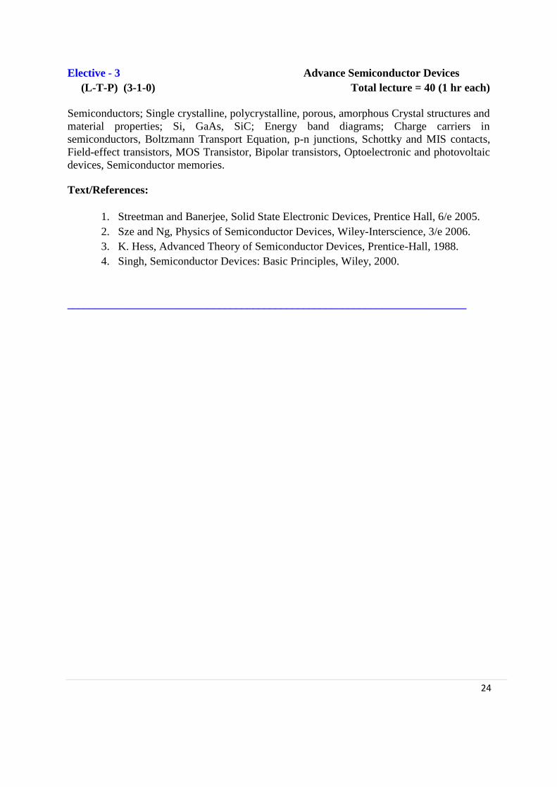
Elective - 3 Advance Semiconductor Devices
(L-T-P) (3-1-0) Total lecture = 40 (1 hr each)
Semiconductors; Single crystalline, polycrystalline, porous, amorphous Crystal structures and
material properties; Si, GaAs, SiC; Energy band diagrams; Charge carriers in
semiconductors, Boltzmann Transport Equation, p-n junctions, Schottky and MIS contacts,
Field-effect transistors, MOS Transistor, Bipolar transistors, Optoelectronic and photovoltaic
devices, Semiconductor memories.
Text/References:
1. Streetman and Banerjee, Solid State Electronic Devices, Prentice Hall, 6/e 2005.
2. Sze and Ng, Physics of Semiconductor Devices, Wiley-Interscience, 3/e 2006.
3. K. Hess, Advanced Theory of Semiconductor Devices, Prentice-Hall, 1988.
4. Singh, Semiconductor Devices: Basic Principles, Wiley, 2000.
_______________________________________________________________________
25
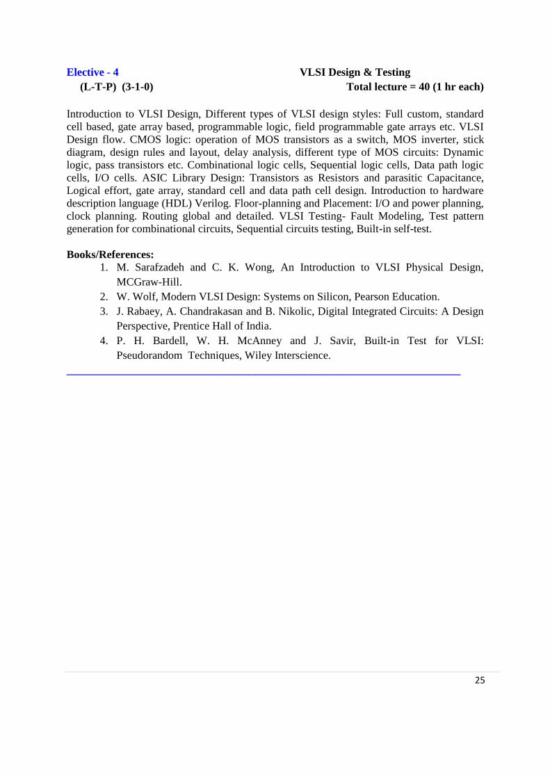
Elective - 4 VLSI Design & Testing
(L-T-P) (3-1-0) Total lecture = 40 (1 hr each)
Introduction to VLSI Design, Different types of VLSI design styles: Full custom, standard
cell based, gate array based, programmable logic, field programmable gate arrays etc. VLSI
Design flow. CMOS logic: operation of MOS transistors as a switch, MOS inverter, stick
diagram, design rules and layout, delay analysis, different type of MOS circuits: Dynamic
logic, pass transistors etc. Combinational logic cells, Sequential logic cells, Data path logic
cells, I/O cells. ASIC Library Design: Transistors as Resistors and parasitic Capacitance,
Logical effort, gate array, standard cell and data path cell design. Introduction to hardware
description language (HDL) Verilog. Floor-planning and Placement: I/O and power planning,
clock planning. Routing global and detailed. VLSI Testing- Fault Modeling, Test pattern
generation for combinational circuits, Sequential circuits testing, Built-in self-test.
Books/References:
1. M. Sarafzadeh and C. K. Wong, An Introduction to VLSI Physical Design,
MCGraw-Hill.
2. W. Wolf, Modern VLSI Design: Systems on Silicon, Pearson Education.
3. J. Rabaey, A. Chandrakasan and B. Nikolic, Digital Integrated Circuits: A Design
Perspective, Prentice Hall of India.
4. P. H. Bardell, W. H. McAnney and J. Savir, Built-in Test for VLSI:
Pseudorandom Techniques, Wiley Interscience.
_______________________________________________________________________
26
Elective - 5 VLSI Technology
(L-T-P) (3-1-0) Total lecture = 40 (1 hr each)
Basics of VLSI Technology, Fundamentals of materials: crystalline versus amorphous
structure, and the characteristics of semiconductors, insulators, and conductors. Processes:
Crystal growth diffusion, Ion Implantation, Oxidation, Photo-lithographic techniques, Photo-
resist, Chemical Vapor Deposition Technology, metallization technique, Etching: Wet
Processing, dry etching, Plasma Etching, Fabrication: pn- Junction, CMOS
Books/References:
1. Ben G Streetman, S Banerjee, “Solid State Electronic Devices,” 5th Edition, Prentice Hall
Inc.
2. S. M. Sze, VLSI Technology, Mcgraw –Hill, 1983
3. Marc J. Madou, Fundamentals of Microfabrication, CRC Press, 1997
_______________________________________________________________________
27
Elective - 6 Foundation of VLSI CAD
(L-T-P) (3-1-0) Total lecture = 40 (1 hr each)
Matrices: Linear dependence of vectors, solution of linear equations, bases of vector spaces,
orthogonality, complementary orthogonal spaces and solution spaces of linear equations;
Graphs: representation of graphs using matrices; Paths, connectedness; circuits, cutsets, trees;
Fundamental circuit and cutset matrices; Voltage and current spaces of a directed graph and
their complementary orthogonality.;Algorithms and data structures: efficient representation
of graphs; Elementary graph algorithms involving bfs and dfs trees, such as finding
connected and 2- connected components of a graph, the minimum spanning tree, shortest path
between a pair of vertices in a graph; Data structures such as stacks, linked lists and queues,
binary trees and heaps. Time and space complexity of algorithms.
Books/References:
1. K. Hoffman and R.E. Kunze, Linear Algebra, Prentice Hall (India), 1986.
2. N.Balabanian and T.A. Bickart, Linear Network Theory : Analysis, Properties, Design
and Synthesis, Matrix Publishers, Inc., 1981.
3. T.Cormen, C.Leiserson and R.A.Rivest, Algorithms, MIT Press and McGraw-Hill,
1990
_______________________________________________________________________
28
Elective - 7 MEMS/NEMS
(L-T-P) (3-1-0) Total lecture = 40 (1 hr each)
Overview: VLSI and Micro-electromechanical Technologies, materials for MEMS.
Actuationtechniques: Electrostatic, Electromagnetic, Thermal, Piezoelectric,
Micromachining: Surfacemicromachining, bulk micromachining, LIGA, Non-Silicon
micromachining techniques: PCB, LCP, PDMS/SU8, Case studies: MEMS/RF
MEMS/BioMEMS
MEMS and NEMS basics, Limitations of Silicon device Fabrication, basic microfabrication
techniques, MEMS fabrication techniques, Nanofabrication Techniques, Material aspects of
MEMS and NEMS (Si, Ge, Metals, Harsh-environment semiconductors, GaAs, InP and
related III-V materials, Ferroelectric materials)
MEMS and NEMS devices and applications, Carbon Nanotube sensor concepts-design
considerations, fabrication of the CNT sensors and state of art applications.
Failure mechanism of MEMS/NEMS devices: failure modes and failure mechanisms, stiction
and charge related failure mechanisms, creep, fatigue, wear and packaging related failures.
Bio-MEMS fabrication technologies
Introduction to bio-MEMS. Nanomaterials for bio-MEMS, Bulk/surface micromachining,
UV Lithography, the LIGA Process, nano-imprinting, hot embossing for Lab-on-a-chip
application; Soft fabrication and polymers soft-lithography, micro-molding, micro-stereo
lithography, thick-film deposition, SAMs. Sensing technologies for Bio-MEMS application
Books/Reference:
1. Stephen D Santuria, Microsystem Design, Kluwer Academic, 2001
2. Marc J. Madou, Fundamentals of Microfabrication, CRC Press, 1997
3. Hector J. De Los Santos, "RF MEMS Circuit Design for Wireless Applications",
ArtechHouse, 2002
4. MEMS & Microsystem, Design and manufacture by Tai-Ran Hsu , McGraw Hill
_______________________________________________________________________
29
Elective - 8 Analog IC design
(L-T-P) (3-1-0) Total lecture = 40 (1 hr each)
CMOS Analog Design
Basic concepts of transistors and diodes, their modeling, large signal and small signal
analysis, CMOS technology, clock feedthrough; Reference sources : bias circuits, bandgap
reference circuit, cascode current mirror; Single stage amplifier, common source amplifier,
drain and gate amplifier, differential amplifier; Operational amplifier; Comparators; Switched
capacitor circuits; Introduction to data converters; Issues of analog layout and device noise.
Text/References:
1. R.Jacob Baker,H.W.Li, and D.E. Boyce CMOS Circuit Design ,Layout and
Simulation, Prentice-Hall of ,1998.
2. Mohammed Ismail and Terri Faiz Analog VLSI Signal and Information Process,
McGraw-Hill Book company,1994.
3. Paul R. Gray and R.G.Meyer, Analysis and design of Analog Integrated circuits John
Wiley and sons,,(3rd Edition),1993.
4. B. Razavi, RF Microelectronics, Prentice-Hall PTR,1998.
_______________________________________________________________________
30
Elective - 9 Embedded System
(L-T-P) (3-1-0) Total lecture = 40 (1 hr each)
Introduction: Embedded system, software embedded in system, embedded system on chip in
VLSI circuit, Categories and requirements of embedded systems, Challenges and issues
related to embedded software developments, Embedded system Design: Concepts of
concurrency, processes, threads, mutual exclusion and inter-process communication, Models
and languages for embedded software, Synchronous approach to embedded system design,
Scheduling paradigms, Scheduling, Algorithms, Hardware/Software Co-design, Introduction
to RTOS: Basic Design using RTOS, Interfacing, RISC Processor: Architecture, Memory,
Reset and Interrupt, Functions, Parallel I/O ports, Timers/Counters, Serial Communication,
Analog Interfaces Case Studies and Applications of embedded systems
Books/References:
1. Raj Kamal, Embedded Systems, TMH
2. Franc Vahid, Tony Givargis, Embedded System Design: A Unified
Hardware/Software Introduction, John Wiley.
_______________________________________________________________________
31
Elective – 10 CAD for VLSI Design
(L-T-P) (3-1-0) Total lecture = 40 (1 hr each)
Overview of design flow and methodologies; Schematic and Layout editors; Overview of
CIF; Partitioning algorithms; Placement algorithms; Routing algorithms; HDL based design
flow and CAD tools; High level synthesis algorithms; Simulation tools and logic simulation
mechanisms; Future trends. The laboratory component will have a mini project covering the
design and implementation of the above CAD; mini project. (Either VHDL or Verilog will be
used as the HDL for the laboratory.)
Books/References:
1. Khosrow Golshan, Physical Design Essentials: An ASIC Design Implementation
Perspective
2. Michael John Sebastian Smith, Application-Specific Integrated Circuits, Addison-
Wesley
_______________________________________________________________________
Recommended