First Edition
T-51383L070J-FW-P-AA OPTREX CORPORATION Page-1/22
LCD Module Technical Specification
T-51383L070J-FW-P-AA
Table of Contents 1. Applications........................................................................................................................................................... 2
2. Features ..................................................................................................................................................................... 2
3. Mechanical Specifications ......................................................................................................................... 2
4. Mechanical Drawing TFT LCD Module..................................................................................... 3
5. Input / Output Terminals .......................................................................................................................... 4
6. Absolute Maximum Ratings ..................................................................................................................... 6
7. Electrical Characteristics............................................................................................................................... 6
8. Power Sequence ......................................................................................................................................... 15
9. Optical Characteristics................................................................................................................................ 16
10. Handing Cautions........................................................................................................................................... 17
11. Reliability TEST ............................................................................................................................................. 22
12. Block Diagram....................................................................................................................................................23
Checked by (Design Engineering Div.)
Checked by (Quality Assurance Div.)
Prepared by (Production Div.)
Revision HistoryRev. Date Page Comment
Jan 1, 2001Final Revision
******
O P T R E X

T-51383L070J-FW-P-AA OPTREX CORPORATION Page-2/22
1. Application
This technical specification applies to 7.0” color TFT-LCD module. The applications of thepanel are car TV, portable DVD,GPS, multimedia applications and others AV system.
2. Features
. Compatible with NTSC & PAL system . Pixel in stripe configuration
. Slim and compact
. High Brightness
. Image Reversion:Up/Down and Left/Right
. Multi Video Display Mode
3. Mechanical Specifications
Parameter Specifications UnitScreen Size 7.0 (16:9 diagonal) inch
Display Format 1440 (H) ×234(V) dot
Active Area 154.08 (H)×87.05 (V) mm
Dot Pitch 0.107(H)×0.372 (V) mm
Pixel Configuration StripeOutline Dimension 167.1 (W)×102.0 (H)×12.0 (D)(typ.) mmSurface Treatment Anti-Glare and Hard Coating
Weight 205±10 g

T-51383L070J-FW-P-AA OPTREX CORPORATION Page-3/22
4. Mechanical Drawing of TFT-LCD Module

T-51383L070J-FW-P-AA OPTREX CORPORATION Page-4/22
5. Input / Output Terminals
5-1) TFT-LCD Panel Driving The interface connector is 6210-30P Series manufactured by ELCO or equivalent.
(0.5mm pitch 30 pin) The connector interface pin assignments are listed in the Table below.
Pin No Symbol I/O Description Remark
1 PSI O Synchronize Pulse for Decoder
2 VR I Red Video Input
3 VG I Green Video Input
4 VB I Blue Video Input
5 GND I Ground
6 CSY I Composite Sync Input
7 NC No Connection
8 NC No Connection
9 NC No Connection
10 NC No Connection
11 MODE 1 I Display mode selection pin 1 (refer to 5.2)
12 MODE 2 I Display mode selection pin 2 (refer to 5.2)
13 MODE 3 I Display mode selection pin 3 (refer to 5.2)
14 GND I Ground
15 BLK O Video Signal Mask Timing Output
16 HSY O Horizontal Sync Output
17 VSY O Vertical Sync Output
18 VDD I Input Voltage For Logic/Logic Voltage For Source Driver
19 NC No Connection
20 FRP O Video Polarity Control Signal
21 GND I Ground
22 U/D I Scanning Direction : (Low : Normal , High : Reverse)
23 L/R I Scanning Direction : (Low : Normal , High : Reverse)
24 N/P I NTSC/PAL Selection Signal(Low : PAL , High : NTSC)
25 NC No Connection
26 NC No Connection
27 GND I Ground
28 VCC I Analog Voltage For Source Driver/Logic Voltage For Gate
29 VGH I Positive Voltage For Gate Driver
30 VGL I Negative Voltage For Gate Driver
T-51383L070J-FW-P-AA OPTREX CORPORATION Page-5/22
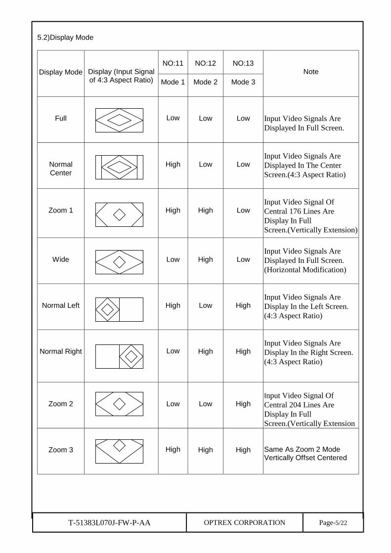
5.2)Display Mode
NO:11 NO:12 NO:13Display Mode Display (Input Signal
of 4:3 Aspect Ratio) Mode 1 Mode 2 Mode 3
Note
Full Low Low Low Input Video Signals AreDisplayed In Full Screen.
NormalCenter
High Low LowInput Video Signals AreDisplayed In The CenterScreen.(4:3 Aspect Ratio)
Zoom 1 High High LowInput Video Signal OfCentral 176 Lines AreDisplay In FullScreen.(Vertically Extension)
Wide Low High LowInput Video Signals AreDisplayed In Full Screen.(Horizontal Modification)
Normal Left High Low HighInput Video Signals AreDisplay In the Left Screen.(4:3 Aspect Ratio)
Normal Right Low High HighInput Video Signals AreDisplay In the Right Screen.(4:3 Aspect Ratio)
Zoom 2 Low Low HighInput Video Signal OfCentral 204 Lines AreDisplay In FullScreen.(Vertically Extension
Zoom 3 High High High Same As Zoom 2 ModeVertically Offset Centered

T-51383L070J-FW-P-AA OPTREX CORPORATION Page-6/22
6 Absolute Maximum Ratings:The followings are maximum values , which if exceeded, may cause faulty operation or damageto the unit.
Parameter Symbol MIN. MAX. Unit Remark
VCC -0.5 7 VSupply Voltage For Source Driver
VDD -0.5 7 V
VGH- VGL -0.3 40 V
H Level VGH 0 40 VSupply Voltage For Gate Driver
L Level VGL -20 0 V
Analog Signal Input Level VR,VG,VB -0.3 7.0 V Note 6-1
Digital Input Signals -0.3 5.5 V
Digital Output Signals -0.3 5.5 V
Storage Temperature -30 +80 ℃
Operation Temperature -20 +70 ℃ Note 6-2
Notes:6-1 Analog Input Voltage means VR,VG,VB.Notes:6-2 Operating Temperature define that contrast, response time, other display
optical character are Ta=+25.
7 Electrical Characteristics 7-1) Recommended Driving condition for TFT-LCD panel
Parameter Symbol MIN. Typ MAX Unit Remark
Analog VCC 4.5 5.0 5.5 VSupply Voltage For SourceDriver Logic VDD 4.5 5.0 5.5 V
H level VGH +15 +17 +19 VSupply Voltage For Gate Driver
L level VGL -16 -15 -14 V
Supply Voltage For controller VDD 4.5 5.0 5.5 VAnalog Signal input Level Amplitude 0.3 VCC-0.3 V
H level VIN 0.7V
- VDD VDigital input voltage
L level VIL -0.3 - 0.3 VDD V
H level VOH 0.7V
- VDD VDigital output voltage
L level VOL -0.3 - 0.3 VDD V
7-2) Backlight driving & Power Consumption
Pin No Symbol Description Remark1 VL1 Input terminal (Hi voltage side) Wire color: pink2 NC No Connection3 VL2 Input terminal (Low voltage side) Wire color: white Note 7-1
T-51383L070J-FW-P-AA OPTREX CORPORATION Page-7/22
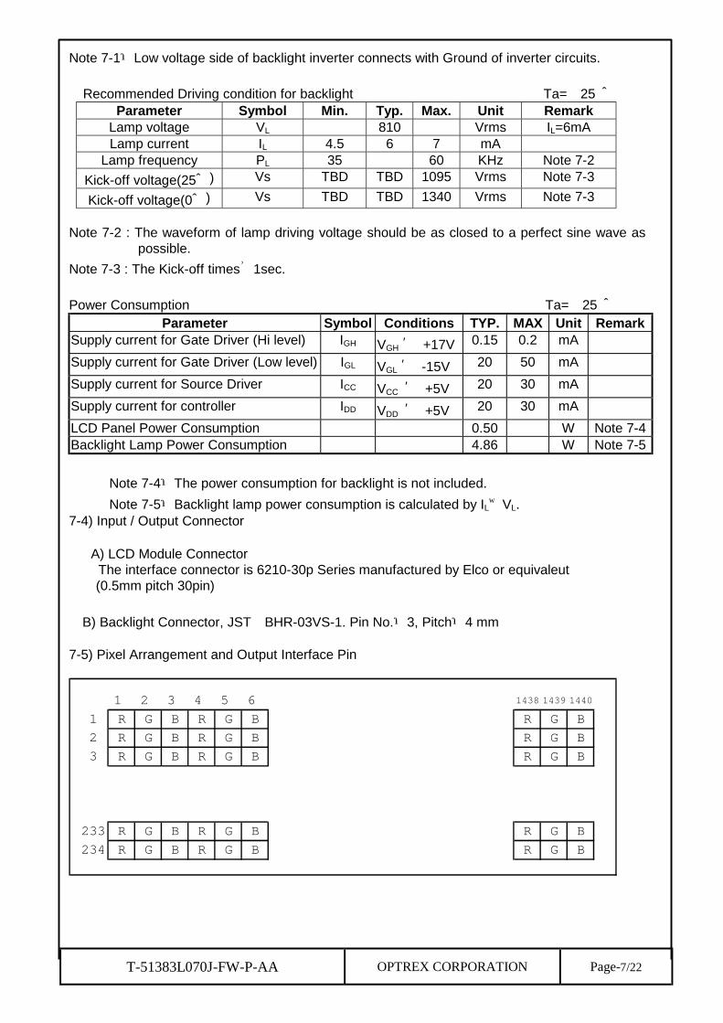
Note 7-1:Low voltage side of backlight inverter connects with Ground of inverter circuits.
Recommended Driving condition for backlight Ta= 25 ℃Parameter Symbol Min. Typ. Max. Unit Remark
Lamp voltage VL 810 Vrms IL=6mALamp current IL 4.5 6 7 mA
Lamp frequency PL 35 60 KHz Note 7-2
Kick-off voltage(25℃) Vs TBD TBD 1095 Vrms Note 7-3
Kick-off voltage(0℃) Vs TBD TBD 1340 Vrms Note 7-3
Note 7-2 : The waveform of lamp driving voltage should be as closed to a perfect sine wave aspossible.
Note 7-3 : The Kick-off times≧1sec.
Power Consumption Ta= 25 ℃Parameter Symbol Conditions TYP. MAX Unit Remark
Supply current for Gate Driver (Hi level) IGH VGH = +17V 0.15 0.2 mA
Supply current for Gate Driver (Low level) IGL VGL = -15V 20 50 mA
Supply current for Source Driver ICC VCC = +5V 20 30 mA
Supply current for controller IDD VDD = +5V 20 30 mA
LCD Panel Power Consumption 0.50 W Note 7-4Backlight Lamp Power Consumption 4.86 W Note 7-5
Note 7-4:The power consumption for backlight is not included.
Note 7-5:Backlight lamp power consumption is calculated by IL×VL.7-4) Input / Output Connector
A) LCD Module ConnectorThe interface connector is 6210-30p Series manufactured by Elco or equivaleut
(0.5mm pitch 30pin)
B) Backlight Connector, JST BHR-03VS-1. Pin No.:3, Pitch:4 mm
7-5) Pixel Arrangement and Output Interface Pin
1 2 3 4 5 6 1438 1439 1440
1 R G B R G B R G B
2 R G B R G B R G B
3 R G B R G B R G B
233 R G B R G B R G B
234 R G B R G B R G B

T-51383L070J-FW-P-AA OPTREX CORPORATION Page-8/22
7-6)Signal Timing Waveforms
Timing Specification [Horizontal]
Parameter Symbol Condition NTSC PAL Unit Notes
Horizontal StartPosition
HPOS - 11.35 11.54 usec Note7-6
Horizontal DisplayArea
HDIS - 50.01 50.36 usec
Notes :7-6
1. Sampling start based on the composite sync falling edge. 2. This value is default , if you want to charge ,please contact PVI.
[Vertical]
Display ModeParamet
erSymbol Condition Full
NormalWide
Zoom
1
Zoom
2
Zoom
3
Unit Notes
NTSC ODD
EVEN
22
286
22
286
52
315
38
301
53
315Line Note 7-7
Vertical
Start
Position
VPOSPAL ODD
EVEN
26
339
26
363
62
375
50
363
62
375Line Note 7-7
NTSC 234 234 176 204 204 LineVertical
Display
Position
VDIS
PAL 281 281 210 234 234 Line
Notes :7-7 Sampling start line number base on the vertical sync pulse (SYNC).
4.67(4.70)usec
SYNC 1.0 Vp-p
3.12(3.32)usec
5V
HSY0V
4.67(4.70)usec
1 Line = 63.56 (64.00)usec
+0.7V
R,G,B0V
50.01(50.36)usec
Display Area11.35(11.54)usec
Note:7-7 Values in brackets correspond to PAL mode (fH=15.734(15.625)KHZ ).

T-51383L070J-FW-P-AA OPTREX CORPORATION Page-9/22
7-7) Display Time Range
A) When sync. signal of NTSC system is applied.
a) Horizontally
11.35 ~ 61.36 μs.
b) Vertical
22 ~ 255 H
B) When sync. signal of PAL system is applied.
a) Horizontally
11.54 ~ 61.9μs
b) Vertical
28 ~ 300 H
T-51383L070J-FW-P-AA OPTREX CORPORATION Page-10/22
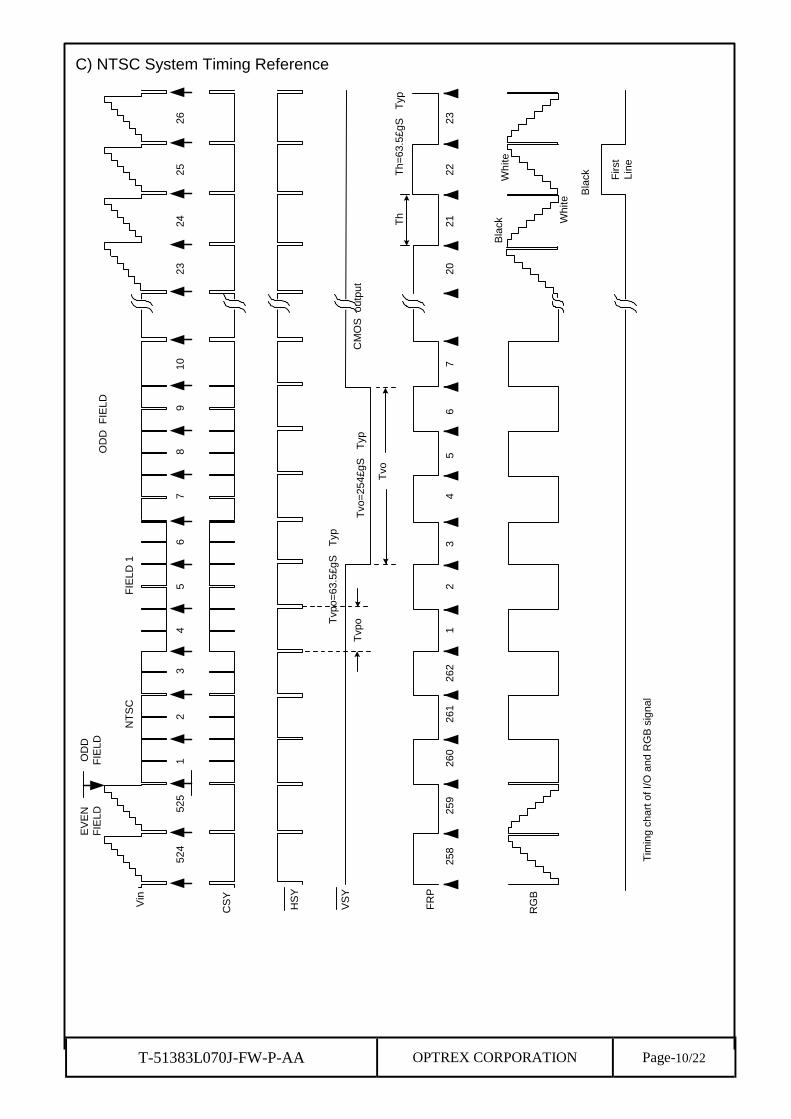
C) NTSC System Timing Reference
Tvo
=254£gS
T
yp
Vin
CS
Y
HS
Y
VS
Y
FR
P
RG
B
OD
DF
IELD
EV
EN
FIE
LD
OD
D F
IELD
524
525
12
34
56
78
910
23
24
25
26
NT
SC
FIE
LD
1
CM
OS
outp
ut
258
259
260
261
262
12
34
56
720
21
22
23
Th
Th=
63.5
£gS
T
yp
Tvo
Tvp
o=
63.5
£gS
T
yp
Tvp
o
Bla
ck
Bla
ck
Wh
ite
Wh
ite
First
Lin
e
Tim
ing
ch
art
of
I/O
an
d R
GB
sig
na
l

T-51383L070J-FW-P-AA OPTREX CORPORATION Page-11/22
26
22
63
26
42
65
26
62
67
26
82
69
27
02
71
27
22
85
28
62
87
28
8
NT
SC
FIE
LD
2
EV
EN
F
IEL
D
Vin
CS
Y
HS
Y
VS
Y
FR
P
RG
B
First
line
EV
EN
FIE
LD
OD
DF
IEL
D
25
92
60
26
12
62
26
31
23
45
62
02
12
21
9
Tvo
=254£gS
T
yp
Tvo
Tvp
e=
95£gS
T
yp
Tvp
e
Tim
ing
ch
art
of
I/O
an
d R
GB
sig
na
l
Wh
ite
Wh
iteB
lack
Bla
ck

T-51383L070J-FW-P-AA OPTREX CORPORATION Page-12/22
D) PAL System Timing Reference
Tvo
=3
18
£g
S
Typ
Vin
CS
Y
HS
Y
VS
Y
FR
P
RG
B
OD
DF
IELD
EV
EN
FIE
LDO
DD
F
IEL
D
622
623
624
625
12
34
56
72
32
42
52
6
PA
L
CM
OS
outp
ut
310
311
312
313
12
34
56
72
12
32
42
5
Th
Th
=6
3.5
£g
S
Typ
Tvo
Tvp
o=
64
£g
S
Typ
Tvp
o
First
Line
Tim
ing c
hart
of I/O
and R
GB
sig
nal
FIE
LD
1
21
22
22
26
27
28
Bla
ck
Wh
ite
Bla
ck
Wh
ite
28
27

T-51383L070J-FW-P-AA OPTREX CORPORATION Page-13/22
309
310
311
312
313
314
315
316
317
318
336
337
338
339
CS
Y
HS
Y
VS
Y
FR
P
RG
B
First
line
EV
EN
FIE
LDO
DD
FIE
LD
308
309
310
311
312
12
34
524
25
26
Bla
ck
23
Tvo
=318£gS
T
yp Tvo
Tvp
e=
32£gS
T
yp
Tvp
e
Tim
ing c
hart
of I
/O a
nd R
GB
sig
nal
335
22
27
28
29
340
341
Wh
ite
Wh
iteB
lack
Wh
ite
Wh
iteB
lack

T-51383L070J-FW-P-AA OPTREX CORPORATION Page-14/22
E) Display Timing (NTSC)
Tvo
=254£gS
T
yp
Vin
CS
Y
HS
Y
VS
Y
FR
P
RG
B
OD
DF
IELD
EV
EN
FIE
LD
OD
D F
IELD
524
525
12
34
56
78
910
23
24
25
26
NT
SC
FIE
LD
1
CM
OS
outp
ut
258
259
260
261
262
12
34
56
720
21
22
23
Th
Th=
63.5
£gS
T
yp
Tvo
Tvp
o=
63.5
£gS
T
yp
Tvp
o
Bla
ck
Bla
ck
Wh
ite
Wh
ite
First
Lin
e
Tim
ing
ch
art
of
I/O
an
d R
GB
sig
na
l

T-51383L070J-FW-P-AA OPTREX CORPORATION Page-15/22
F) Display Timing (PAL)
11.5
4µs
Th
o=
4.7
µs
64µ
s
2.1
µs5
0.3
6 µ
s
50
.36
/64
=7
9%
Dis
play
Tim
e
Sam
plin
g C
lock
: 9.5
3M
Hz
(1)
Horiz
onta
l Tim
ing
(2)
Ve
rtic
al T
imin
g
Vin
OD
DF
IELD
EV
EN
FIE
LDO
DD
F
IEL
D
622
623
624
625
12
34
56
72
22
32
42
5
PA
LF
IELD
1
20
21
Tvo
=5
H T
ypV
SY
Tvo
Tvp
o=
1H
T
yp
Tvp
o
309
310
311
312
313
314
315
316
317
318
334
335
336
33 7
PA
LF
IELD
2
EV
EN
F
IEL
D
Vin
EV
EN
FIE
LDO
DD
FIE
LD
333
338
339
VS
YT
vo=
5H
Typ T
vo
Tvp
e=
0.5
H T
yp
Tvp
e
8.5
H2
8H
First
Lin
e23
4 H
Not D
ispla
y T
ime
79
.4/3
17
.5=
25
%
Dis
pla
y T
ime
23
4/3
17
.5=
75
%
28
.5H
T-51383L070J-FW-P-AA OPTREX CORPORATION Page-16/22
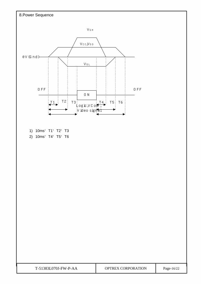
8.Power Sequence
1) 10ms≦T1≦T2≦T3
2) 10ms≦T4≦T5≦T6
0V(Gnd)
VGH
VCC,VDD
VGL
ONOFF
T1 T2 T3 T4 T5 T6
OFF
Logic,VCom,Video signal
T-51383L070J-FW-P-AA OPTREX CORPORATION Page-17/22
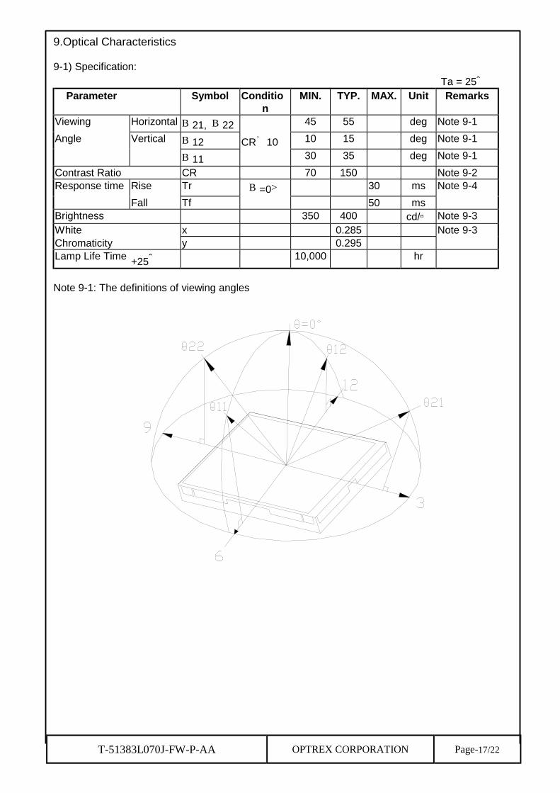
9.Optical Characteristics
9-1) Specification:
Ta = 25℃Parameter Symbol Conditio
nMIN. TYP. MAX. Unit Remarks
Viewing Horizontal θ21, θ22 45 55 deg Note 9-1
Angle Vertical θ12 CR≧10 10 15 deg Note 9-1
θ11 30 35 deg Note 9-1
Contrast Ratio CR 70 150 Note 9-2Response time Rise Tr θ=0° 30 ms Note 9-4
Fall Tf 50 msBrightness 350 400 cd/㎡ Note 9-3White x 0.285 Note 9-3Chromaticity y 0.295Lamp Life Time +25℃ 10,000 hr
Note 9-1: The definitions of viewing angles

T-51383L070J-FW-P-AA OPTREX CORPORATION Page-18/22
Luminance when Testing point is WhiteNote 9-2:CR = Luminance when Testing point is Black
(Testing configuration see 8-2 )Contrast Ratio is measured in optimum common electrode voltage.
Note 9-3:Topcon BM-7(fast) luminance meter 2°field of view is used in the testing (after 20~30 minutes operation).
Lamp Current 6mA
Note 9-4: The definition of response time:
100%
90%
10%
0%
White White
Brig
htn
ess
Black
Tr Tf

T-51383L070J-FW-P-AA OPTREX CORPORATION Page-19/22
9-2) Testing configuration
LCD Display
R, G, B Waveform of Pattern A at Testing Point
R, G, B Waveform of Pattern B at Testing Point
500mm
BM-7(fast)
LCD
Backlight
R,G,B signal
Patterngenerator
input
Pattern A Pattern B
Testing Point Testing Point
16ms 16ms
16ms 16ms
Caution: 1. Environmental illumination≦1 lux 2. Before test CR, Vcom voltage must
be adjusted carefully to get the bestCR.
Vcom
RGB
waveform
RGB
waveform
Vcom

T-51383L070J-FW-P-AA OPTREX CORPORATION Page-20/22
10. Handling Cautions 10-1) Mounting of module
a) Please power off the module when you connect the input/output connector.b) Please connect the ground pattern of the inverter circute surely. If the
connection is not perfect, some following problems may happen possibly. 1.The noise from the backlight unit will increase. 2.The output from inverter circuit will be unstable. 3.In some cases a part of module will heat.
c) Polarizer which is made of soft material and susceptible to flaw must be handled carefully. d) Protective film (Laminator) is applied on surface to protect it against scratches and dirts. It is recommended to peel off the laminator before use and taking care of static electricity. 10-2) Precautions in mounting
a) When metal part of the TFT-LCD module (shielding lid and rear case) is soiled,wipe it with soft dry cloth.
b) Wipe off water drops or finger grease immediately. Long contact with watermay cause discoloration or spots.
c) TFT-LCD module uses glass which breaks or cracks easily if dropped orbumped on hard surface. Please handle with care.
d) Since CMOS LSI is used in the module. So take care of static electricity andearth yourself when handling.
10-3) Adjusting modulea) Adjusting volumes on the rear face of the module have been set optimally
before shipment.b) Therefore, do not change any adjusted values. If adjusted values are changed,
the specifications described may not be satisfied. 10-4) Others
a) Do not expose the module to direct sunlight or intensive ultraviolet rays formany Hours.
b) Store the module at a room temperature place.c) The voltage of beginning electric discharge may over the normal voltage
because of leakage current from approach conductor by to draw lump readlead line around.
d) If LCD panel breaks, it is possibly that the liquid crystal escapes from thepanel.Avoid putting it into eyes or mouth. When liquid crystal sticks on hands,clothes or feet. Wash it out immediately with soap.
e) Observe all other precautionary requirements in handling general electroniccomponents.
f) Please adjust the voltage of common electrode as material of attachment by 1module.

T-51383L070J-FW-P-AA OPTREX CORPORATION Page-21/22
11. Reliability Test
No Test Item Test Condition
1 High Temperature Storage Test Ta = +80 ℃, 240 hrs
2 Low Temperature Storage Test Ta = -30℃, 240 hrs
3 High Temperature Operation Test Ta = +70 ℃, 240 hrs
4 Low Temperature Operation Test Ta = -20 ℃, 240 hrs
5High Temperature & High
Humidity Operation TestTa = +60℃, 95%RH, 240 hrs
6Thermal Cycling Test
(non-operating)
-25℃ →+25℃→ +70℃, 200 Cycles
30 min 5min 30 min
7Vibration Test
(non-operating)
Frequency:10 ~ 55 HZ
Amplitude:1.5 mm
Sweep time: 11 mins
Test Period: 6 Cycles for each direction of X, Y, Z
8Shock Test
(non-operating)
100G, 6ms
Direction: ±X, ±Y, ±Z
Cycle: 3 times
9Electrostatic Discharge Test
(non-operating)
150pF, 330Ω
Air: ±15KV; Contact: ±8KV
10 times/point, 9 points/panel face Ta: ambient temperature
[Criteria]Under the display quality test conditions with normal operation state, there should be nochange which may affect practical display function.

T-51383L070J-FW-P-AA OPTREX CORPORATION Page-22/22
11. Block Diagram
Controller
V Driver(Gate)
LCD Panel
H Driver(Source)
Back-lightInverter
HSYVSYCSY
BLKU/DR/LN/P
Mode 1,2,3FRP
+5 V
+17 V-15V
VRVGVB
R1G1B1
VCO
PLL VL
Recommended