GPU
DP141 OUTP0
Dis
pla
yPo
rt C
on
nec
tor
HPD
ML0
x
GPU
x
DP141
x
DP141
DP0
AUXp
DP1
DP2
DP3
HPD
AUXn
OUTP1
OUTP2
OUTP3
ML1
ML2
ML3
AUXp
AUXn
Copyright © 2016, Texas Instruments Incorporated
Product
Folder
Sample &Buy
Technical
Documents
Tools &
Software
Support &Community
An IMPORTANT NOTICE at the end of this data sheet addresses availability, warranty, changes, use in safety-critical applications,intellectual property matters and other important disclaimers. PRODUCTION DATA.
SN65DP141SLLSES6A –FEBRUARY 2016–REVISED OCTOBER 2016
SN65DP141 DisplayPort Linear Redriver
1
1 Features1• Supports VESA DisplayPort 1.3, and eDP 1.4• Quad Channel Linear Redriver Supporting Data
Rates up to 12 Gbps including DisplayPort RBR,HBR, HBR2 and HBR3
• Protocol Agnostic• Transparent to DP Link Training• Position Independent on the Link Suitable for
Source, Sink and Cable Applications• 15-dB Analog Equalization at 6 GHz• Output Linear Dynamic Range: 1200 mV• Bandwidth: >20 GHz• Better than 16-dB Return Loss at 6 GHz• 2.5-V or 3.3-V ±5% Single Power Supply Option• Low Power Consumption with 80 mW per channel
at 2.5 V VCC
• GPIO or I2C Control
2 Applications• Tablets• Notebooks• Desktops• Docking Stations
3 DescriptionThe SN65DP141 is an asynchronous, protocol-agnostic, low latency, four-channel linear equalizeroptimized for use up to 12 Gbps and compensates forlosses due to board traces and cables.
The device is transparent to DisplayPort (DP) linktraining such a way that a DP source and a sink canperform effective link training overcoming traditional“aux snooping” re-drivers’ shortcomings. Additionally,the device is position independent. It can be placedinside source, cable or sink effectively providing a“negative loss” component to the overall link budget.Linear equalization inside SN65DP141 also increaseslink margin when used with a receiver implementingDecision Feedback Equalization (DFE).
SN65DP141 allows independent channel control forequalization, gain, dynamic range using both I2C andGPIO configurations.
Device Information(1)
PART NUMBER PACKAGE BODY SIZE (NOM)SN65DP141 WQFN (38) 7.00 mm x 5.00 mm
(1) For all available packages, see the orderable addendum atthe end of the data sheet.
Spacer
Spacer
Simplified Schematic

2
SN65DP141SLLSES6A –FEBRUARY 2016–REVISED OCTOBER 2016 www.ti.com
Product Folder Links: SN65DP141
Submit Documentation Feedback Copyright © 2016, Texas Instruments Incorporated
Table of Contents1 Features .................................................................. 12 Applications ........................................................... 13 Description ............................................................. 14 Revision History..................................................... 25 Pin Configuration and Functions ......................... 36 Specifications......................................................... 5
6.1 Absolute Maximum Ratings ...................................... 56.2 ESD Ratings ............................................................ 56.3 Recommended Operating Conditions....................... 56.4 Thermal Information ................................................. 56.5 Electrical Characteristics........................................... 66.6 Switching Characteristics .......................................... 76.7 Switching Characteristics, I2C Interface.................... 76.8 Typical Characteristics .............................................. 8
7 Parameter Measurement Information .................. 98 Detailed Description ............................................ 13
8.1 Overview ................................................................. 138.2 Functional Block Diagram ....................................... 13
8.3 Feature Description................................................. 148.4 Device Functional Modes........................................ 158.5 Register Maps ........................................................ 17
9 Application and Implementation ........................ 239.1 Application Information............................................ 239.2 Typical Application ................................................. 23
10 Power Supply Recommendations ..................... 2511 Layout................................................................... 26
11.1 Layout Guidelines ................................................. 2611.2 Layout Example .................................................... 27
12 Device and Documentation Support ................. 2812.1 Receiving Notification of Documentation Updates 2812.2 Community Resources.......................................... 2812.3 Trademarks ........................................................... 2812.4 Electrostatic Discharge Caution............................ 2812.5 Glossary ................................................................ 28
13 Mechanical, Packaging, and OrderableInformation ........................................................... 28
4 Revision History
Changes from Original (February 2016) to Revision A Page
• Replaced Figure 28 ............................................................................................................................................................. 24
Thermal
Pad
VC
C
1IN0_P
PW
D#
2IN0_N
RX
_G
AIN
3VCC
EQ
_M
OD
E/_
AD
D2
4IN1_P
EQ
0/A
DD
0
5IN1_N
EQ
1/A
DD
1
6VCC
7VCC
OUT0_P
8IN2_P
9IN2_N
VC
C
OUT0_N
VCC
OUT1_P
OUT1_N
VCC
VCC
OUT2_P
OUT2_N
VCC
OUT3_P
OUT3_N
VC
C
VC
CVCC
IN3_P
IN3_N
SD
A
DR
V_
PK
#/S
CL
I2C
_E
N
TX
_D
C_
GA
IN/C
S
RE
XT
10
11
12
13 14 15 16 17 18 19
20
21
22
23
24
25
26
27
28
29
30
31
32333435363738
3
SN65DP141www.ti.com SLLSES6A –FEBRUARY 2016–REVISED OCTOBER 2016
Product Folder Links: SN65DP141
Submit Documentation FeedbackCopyright © 2016, Texas Instruments Incorporated
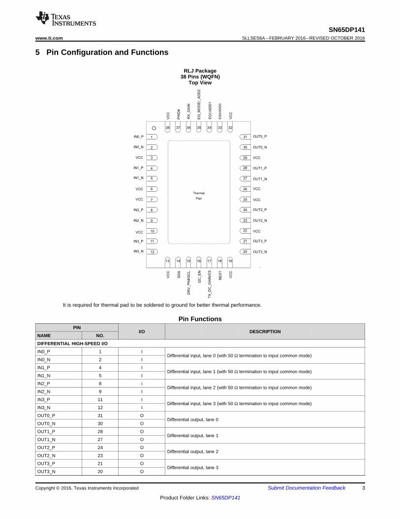
5 Pin Configuration and Functions
RLJ Package38 Pins (WQFN)
Top View
It is required for thermal pad to be soldered to ground for better thermal performance.
Pin FunctionsPIN
I/O DESCRIPTIONNAME NO.
DIFFERENTIAL HIGH-SPEED I/O
IN0_P 1 IDifferential input, lane 0 (with 50 Ω termination to input common mode)
IN0_N 2 I
IN1_P 4 IDifferential input, lane 1 (with 50 Ω termination to input common mode)
IN1_N 5 I
IN2_P 8 iDifferential input, lane 2 (with 50 Ω termination to input common mode)
IN2_N 9 I
IN3_P 11 IDifferential input, lane 3 (with 50 Ω termination to input common mode)
IN3_N 12 I
OUT0_P 31 ODifferential output, lane 0
OUT0_N 30 O
OUT1_P 28 ODifferential output, lane 1
OUT1_N 27 O
OUT2_P 24 ODifferential output, lane 2
OUT2_N 23 O
OUT3_P 21 ODifferential output, lane 3
OUT3_N 20 O

4
SN65DP141SLLSES6A –FEBRUARY 2016–REVISED OCTOBER 2016 www.ti.com
Product Folder Links: SN65DP141
Submit Documentation Feedback Copyright © 2016, Texas Instruments Incorporated
Pin Functions (continued)PIN
I/O DESCRIPTIONNAME NO.
CONTROL SIGNALS
SDA 14 I/O (open drain) GPIO mode:No action needed.
I2C mode:I2C data. Connect a 10-kΩ pull-up resistorexternally.
DRV_PK#/SCL 15I
(with 200-kΩ internalpull-up)
GPIO mode:HIGH: disable Driver peakingLOW: enables Driver 6-dB AC peaking
I2C mode:I2C CLK. Connect a 10-kΩ pull-up resistorexternally.
I2C_EN 16I
(with 200-kΩ internalpull-up)
Configures the device operation for I2C or GPIO mode:HIGH: enables I2C modeLOW: enables GPIO mode
TX_DC_GAIN/CS 17
I(with 200-kΩ Internalpull-down, 2.5V/3.3V
CMOS)
GPIO mode:HIGH: 6 dB DC gain for transmitterLOW: 0 dB DC gain for transmitter
I2C mode:HIGH: acts as Chip SelectLOW: disables I2C interface
REXT 18 I (analog) External Bias Resistor: 1,200 Ω to GND
EQ0/ADD0 33I
(2.5V/3.3V CMOS -3-state)
GPIO mode:Working with RX_GAIN and EQ1 to determine thereceiver DC and AC gain.
I2C mode:ADD0 along with pins ADD1 and ADD2comprise the three bits of I2C slaveaddress. ADD2:ADD1:ADD0:XXX
EQ_MODE/ ADD2 35
I(with 200-kΩ Internalpull-down, 2.5V/3.3V
CMOS )
GPIO mode:HIGH: Trace modeLOW: Cable mode
I2C mode:ADD2 along with pins ADD1 and ADD0comprise the three bits of I2C slaveaddress. ADD2:ADD1:ADD0:XXX
RX_GAIN 36I
(2.5V/3.3V CMOS -3-state)
GPIO mode:Working with EQ0 and EQ1 to determine thereceiver DC and AC gain.
I2C mode:No action needed
PWD# 37
I(with 200-kΩ Internal
pull-up, 2.5V/3.3VCMOS)
HIGH: Normal OperationLOW: Power downs the device, inputs off and outputs disabled, resets I2C
EQ1/ADD1 34I
(2.5V/3.3V CMOS -3-state)
GPIO mode:Working with RX_GAIN and EQ0 to determine thereceiver DC and AC gain.
I2C mode:ADD1 along with pins ADD0 and ADD2comprise the three bits of I2C slaveaddress ADD2:ADD1:ADD0:XXX
POWER SUPPLY
VCC3, 6, 7, 10, 13,19, 22, 25, 26,
29, 32, 38Power Power supply 2.5V ±5%, 3.3V ±5%
GND Center Pad GroundThe ground center pad is the metal contact at the bottom of the package. This pad must beconnected to the GND plane. At least 15 PCB vias are recommended to minimize inductanceand provide a solid ground. Refer to the package drawing (RLJ-package) for the via placement.
5
SN65DP141www.ti.com SLLSES6A –FEBRUARY 2016–REVISED OCTOBER 2016
Product Folder Links: SN65DP141
Submit Documentation FeedbackCopyright © 2016, Texas Instruments Incorporated
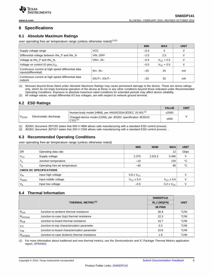
(1) Stresses beyond those listed under Absolute Maximum Ratings may cause permanent damage to the device. These are stress ratingsonly, which do not imply functional operation of the device at these or any other conditions beyond those indicated under RecommendedOperating Conditions. Exposure to absolute-maximum-rated conditions for extended periods may affect device reliability.
(2) All voltage values, except differential I/O bus voltages, are with respect to network ground terminal.
6 Specifications
6.1 Absolute Maximum Ratingsover operating free-air temperature range (unless otherwise noted) (1) (2)
MIN MAX UNITSupply voltage range VCC –0.3 4 VDifferential voltage between INx_P and INx_N VIN, DIFF –2.5 2.5 VVoltage at INx_P and INx_N, VIN+, IN– –0.5 VCC + 0.5 VVoltage on control IO pins,VIO –0.5 VCC + 0.5 VContinuous current at high speed differential datainputs(differential) IN+, IN– –25 25 mA
Continuous current at high speed differential dataoutputs IOUT+, IOUT– –25 25 mA
(1) JEDEC document JEP155 states that 500-V HBM allows safe manufacturing with a standard ESD control process.(2) JEDEC document JEP157 states that 250-V CDM allows safe manufacturing with a standard ESD control process. .
6.2 ESD RatingsVALUE UNIT
V(ESD) Electrostatic dischargeHuman-body model (HBM), per ANSI/ESDA/JEDEC JS-001 (1) ±2000
VCharged-device model (CDM), per JEDEC specification JESD22-C101 (2) ±500
6.3 Recommended Operating Conditionsover operating free-air temperature range (unless otherwise noted)
MIN NOM MAX UNITDR Operating data rate 12 GbpsVCC Supply voltage 2.375 2.5/3.3 3.465 VTC Junction temperature –10 125 °CTA Operating free-air temperature –40 85 °CCMOS DC SPECIFICATIONSVIH Input high voltage 0.8 x VCC VV(MID) Input middle voltage VCC x 0.4 VCC x 0.6 VVIL Input low voltage –0.5 0.2 x VCC V
(1) For more information about traditional and new thermal metrics, see the Semiconductor and IC Package Thermal Metrics applicationreport, SPRA953.
6.4 Thermal Information
THERMAL METRIC (1)SN65DP141
UNITRLJ (WQFN)38 PINS
RθJA Junction-to-ambient thermal resistance 36.9 °C/WRθJC(top) Junction-to-case (top) thermal resistance 22.3 °C/WRθJB Junction-to-board thermal resistance 10.7 °C/WψJT Junction-to-top characterization parameter 0.3 °C/WψJB Junction-to-board characterization parameter 10.6 °C/WRθJC(bot) Junction-to-case (bottom) thermal resistance 1.9 °C/W
6
SN65DP141SLLSES6A –FEBRUARY 2016–REVISED OCTOBER 2016 www.ti.com
Product Folder Links: SN65DP141
Submit Documentation Feedback Copyright © 2016, Texas Instruments Incorporated
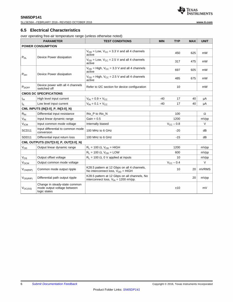
6.5 Electrical Characteristicsover operating free-air temperature range (unless otherwise noted)
PARAMETER TEST CONDITIONS MIN TYP MAX UNITPOWER CONSUMPTION
PDL Device Power dissipation
VOD = Low, VCC = 3.3 V and all 4 channelsactive 450 625 mW
VOD = Low, VCC = 2.5 V and all 4 channelsactive 317 475 mW
PDH Device Power dissipation
VOD = High, VCC = 3.3 V and all 4 channelsactive 697 925 mW
VOD = High, VCC = 2.5 V and all 4 channelsactive 485 675 mW
PDOFFDevice power with all 4 channelsswitched off Refer to I2C section for device configuration 10 mW
CMOS DC SPECIFICATIONSIIH High level input current VIN = 0.9 × VCC -40 17 40 µAIIL Low level input current VIN = 0.1 × VCC -40 17 40 µACML INPUTS (IN[3:0]_P, IN[3:0]_N)RIN Differential input resistance INx_P to INx_N 100 Ω
VIN Input linear dynamic range Gain = 0.5 1200 mVppVICM Input common mode voltage Internally biased VCC – 0.8 V
SCD11 Input differential to common modeconversion 100 MHz to 6 GHz -20 dB
SDD11 Differential input return loss 100 MHz to 6 GHz -15 dBCML OUTPUTS (OUT[3:0]_P, OUT[3:0]_N)VOD Output linear dynamic range RL = 100 Ω, VOD = HIGH 1200 mVpp
RL = 100 Ω, VOD = LOW 600 mVppVOS Output offset voltage RL = 100 Ω, 0 V applied at inputs 10 mVppVOCM Output common mode voltage VCC – 0.4 V
VCM(RIP) Common mode output ripple K28.5 pattern at 12 Gbps on all 4 channels,No interconnect loss, VOD = HIGH 10 20 mVRMS
VOD(RIP) Differential path output ripple K28.5 pattern at 12 Gbps on all channels, Nointerconnect loss, VIN = 1200 mVpp. 20 mVpp
VOC(SS)
Change in steady-state commonmode output voltage betweenlogic states
±10 mV
OMrp - rn
rn rpr 2 x x 100
§ ·¨ ¸'
¹
©
7
SN65DP141www.ti.com SLLSES6A –FEBRUARY 2016–REVISED OCTOBER 2016
Product Folder Links: SN65DP141
Submit Documentation FeedbackCopyright © 2016, Texas Instruments Incorporated
(1) Rise and Fall measurements include board and channel effects of the test environment, refer to Figure 5 and Figure 7.(2) tSK(O) is the magnitude of the time difference between the channels.(3) tSK(PP) is the magnitude of the difference in propagation delay times between any specified terminals of two devices when both devices
operate with the same(4) All noise sources added.
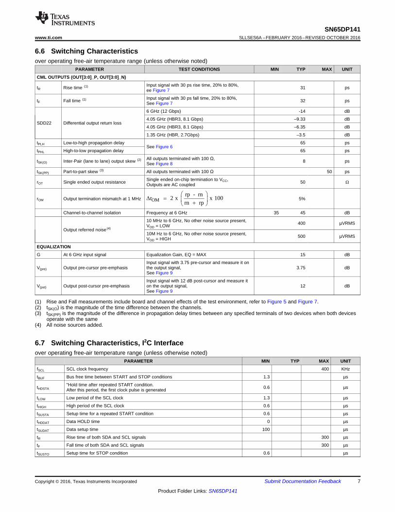
6.6 Switching Characteristicsover operating free-air temperature range (unless otherwise noted)
PARAMETER TEST CONDITIONS MIN TYP MAX UNIT
CML OUTPUTS (OUT[3:0]_P, OUT[3:0]_N)
tR Rise time (1) Input signal with 30 ps rise time, 20% to 80%,ee Figure 7 31 ps
tF Fall time (1) Input signal with 30 ps fall time, 20% to 80%,See Figure 7 32 ps
SDD22 Differential output return loss
6 GHz (12 Gbps) -14 dB
4.05 GHz (HBR3, 8.1 Gbps) –9.33 dB
4.05 GHz (HBR3, 8.1 Gbps) –6.35 dB
1.35 GHz (HBR, 2.7Gbps) –3.5 dB
tPLH Low-to-high propagation delaySee Figure 6
65 ps
tPHL High-to-low propagation delay 65 ps
tSK(O) Inter-Pair (lane to lane) output skew (2) All outputs terminated with 100 Ω,See Figure 8 8 ps
tSK(PP) Part-to-part skew (3) All outputs terminated with 100 Ω 50 ps
rOT Single ended output resistance Single ended on-chip termination to VCC,Outputs are AC coupled 50 Ω
rOM Output termination mismatch at 1 MHz 5%
Channel-to-channel isolation Frequency at 6 GHz 35 45 dB
Output referred noise (4)
10 MHz to 6 GHz, No other noise source present,VOD = LOW 400 µVRMS
10M Hz to 6 GHz, No other noise source present,VOD = HIGH 500 µVRMS
EQUALIZATION
G At 6 GHz input signal Equalization Gain, EQ = MAX 15 dB
V(pre) Output pre-cursor pre-emphasisInput signal with 3.75 pre-cursor and measure it onthe output signal,See Figure 9
3.75 dB
V(pst) Output post-cursor pre-emphasisInput signal with 12 dB post-cursor and measure iton the output signal,See Figure 9
12 dB
6.7 Switching Characteristics, I2C Interfaceover operating free-air temperature range (unless otherwise noted)
PARAMETER MIN TYP MAX UNIT
fSCL SCL clock frequency 400 KHz
tBUF Bus free time between START and STOP conditions 1.3 µs
tHDSTA"Hold time after repeated START condition.After this period, the first clock pulse is generated 0.6 µs
tLOW Low period of the SCL clock 1.3 µs
tHIGH High period of the SCL clock 0.6 µs
tSUSTA Setup time for a repeated START condition 0.6 µs
tHDDAT Data HOLD time 0 µs
tSUDAT Data setup time 100 µs
tR Rise time of both SDA and SCL signals 300 µs
tF Fall time of both SDA and SCL signals 300 µs
tSUSTO Setup time for STOP condition 0.6 µs

−40
−35
−30
−25
−20
−15
−10
−5
0
0 2 4 6 8 10 12 14Frequency (GHz)
Am
plitu
de (
dB)
G004
−45
−40
−35
−30
−25
−20
−15
−10
−5
0
0 2 4 6 8 10 12 14Frequency (GHz)
Am
plitu
de (
dB)
G005
−45
−40
−35
−30
−25
−20
−15
−10
−5
0
0 2 4 6 8 10 12 14Frequency (GHz)
Am
plitu
de (
dB)
G002
−70
−60
−50
−40
−30
−20
−10
0
0 2 4 6 8 10 12 14Frequency (GHz)
Am
plitu
de (
dB)
G003
8
SN65DP141SLLSES6A –FEBRUARY 2016–REVISED OCTOBER 2016 www.ti.com
Product Folder Links: SN65DP141
Submit Documentation Feedback Copyright © 2016, Texas Instruments Incorporated
6.8 Typical Characteristics
Figure 1. Differential Input Return Loss Figure 2. Differential to Common Mode Conversion
Figure 3. Differential Output Return Loss Figure 4. Common Mode Output Return Loss
80%
20% 20%
80%
tr tf
VOD
IN
OUT
tPLH
tPHL
V = 0 VID
V = 0 VOD
1pF
OUT-
50
50
OUT+
VOCM
Copyright © 2016, Texas Instruments Incorporated
9
SN65DP141www.ti.com SLLSES6A –FEBRUARY 2016–REVISED OCTOBER 2016
Product Folder Links: SN65DP141
Submit Documentation FeedbackCopyright © 2016, Texas Instruments Incorporated
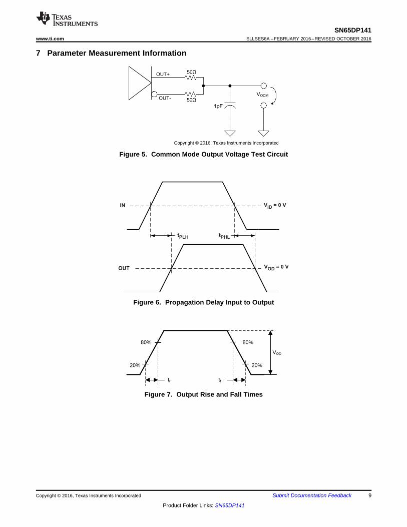
7 Parameter Measurement Information
Figure 5. Common Mode Output Voltage Test Circuit
SPACE
Figure 6. Propagation Delay Input to Output
SPACE
Figure 7. Output Rise and Fall Times
SPACE
PATTERNL= 2" L= 2"
OSCILLOSCOPEGENERATOR RX+EQ
CHARACTERIZATION BOARD
TEST CHANNEL
OUT
SN65DP141
0V
V1
V3
V2
V4
V5
V6Not drawn to scale
tSK(0)
OUTx
OUTy
10
SN65DP141SLLSES6A –FEBRUARY 2016–REVISED OCTOBER 2016 www.ti.com
Product Folder Links: SN65DP141
Submit Documentation Feedback Copyright © 2016, Texas Instruments Incorporated
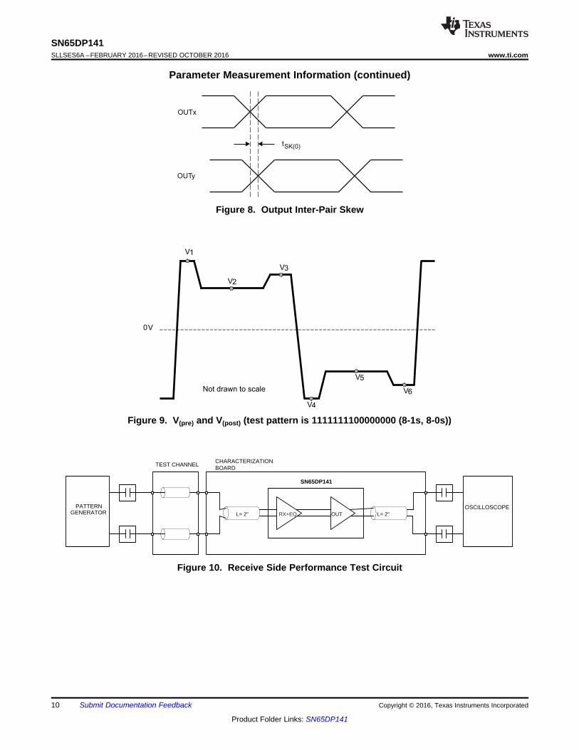
Parameter Measurement Information (continued)
Figure 8. Output Inter-Pair Skew
SPACE
Figure 9. V(pre) and V(post) (test pattern is 1111111100000000 (8-1s, 8-0s))
SPACE
Figure 10. Receive Side Performance Test Circuit
SPACE

48 k
VCC
IN
ESD
VCC
48 k
ESD
Copyright © 2016, Texas Instruments Incorporated
Gain Stage+EQ
RBBDC
VBB
Self-Biasing Network
Line End Termination
VCC
VCC
ESD
IN+
R = 50
T(SE)
R = 50
T(SE)
IN-
Copyright © 2016, Texas Instruments Incorporated
PATTERNL= 2" OUT
TEST CHANNELCHARACTERIZATION BOARD
SN65DP141
OSCILLOSCOPEGENERATOR L= 2"
11
SN65DP141www.ti.com SLLSES6A –FEBRUARY 2016–REVISED OCTOBER 2016
Product Folder Links: SN65DP141
Submit Documentation FeedbackCopyright © 2016, Texas Instruments Incorporated
Parameter Measurement Information (continued)
Figure 11. Transmit Side Performance Test Circuit
Figure 12. Equivalent Input Circuit
SPACE
Figure 13. 3-Level Input Biasing Network

12
SN65DP141SLLSES6A –FEBRUARY 2016–REVISED OCTOBER 2016 www.ti.com
Product Folder Links: SN65DP141
Submit Documentation Feedback Copyright © 2016, Texas Instruments Incorporated
Parameter Measurement Information (continued)
Figure 14. Two - Wire Serial Interface Data Transfer
Figure 15. Two - Wire Serial Interface Timing Diagram

4 Bit Register1 Bit Register1 Bit Register
VCC
200K
50 50
VBB
50 50
Band-Gap Voltage Reference and Bias Current Generation
Power-OnReset
OUT[3:0]_P
I2C_EN
2-Wire Interface and Control Logic
I2C_EN
EQ0/ADD0
EQ1/ADD1
EQ_MODE/ADD2
6 Bit Register
3 Bit Register
General Setting
200K
1.2K
200K 200K 200K
GND
IN[3:0]_P
DRV_PK#/SCL
SDA
PWD#
VOD/CS
GAIN
Input Buffer with Selectable Equalizer Output Driver
VCC
Power-On Reset
OUT[3:0]_P
2 Bit Register
DC Gain
EQ ControlChannel Enable
VOD Swing
AC GainSDA
PWD#
VOD/CS
GAIN
DRV_PK#/SCL
EQ1/ADD1
EQ0/ADD0
EQ_MODE/ADD2
IN[3:0]_N
Copyright © 2016, Texas Instruments Incorporated
13
SN65DP141www.ti.com SLLSES6A –FEBRUARY 2016–REVISED OCTOBER 2016
Product Folder Links: SN65DP141
Submit Documentation FeedbackCopyright © 2016, Texas Instruments Incorporated
8 Detailed Description
8.1 OverviewThe SN65DP141 is an asynchronous, protocol-agnostic, low latency, four-channel linear equalizer optimized foruse up to 12 Gbps. The characteristics of this device make it transparent to DisplayPort (DP) link training, itsupports all the available DP bit rates from RBR to HBR3 (1.6 Gbps, 2.7 Gbps, 5.4 Gbps and 8.1 Gbpsrespectively). Additionally, the SN65DP141 is configurable to a trace or cable mode, and hence improves itsperformance depending on the type of channel it is being used. Its transparency to the DP link training makes theSN65DP141 a position independent device, suitable for source/sink or cable applications, effectively providing a“negative loss” component to the overall link budget, in order to compensate the signal degradation over thechannel.
The SN65DP141 is configurable by means of I2C and GPIOs, allowing independent channel control foractivation, equalization, gain, dynamic range.
8.2 Functional Block Diagram
INx_P
INx_N
OUTx_P
OUTx_N
TX_GAIN(TX_DC_GAIN)EQUALIZATION(EQ_AC_GAIN)RX_GAIN(EQ_DC_GAIN)
0dB or -6dB Up to 15dB 0dB or 6dB
14
SN65DP141SLLSES6A –FEBRUARY 2016–REVISED OCTOBER 2016 www.ti.com
Product Folder Links: SN65DP141
Submit Documentation Feedback Copyright © 2016, Texas Instruments Incorporated
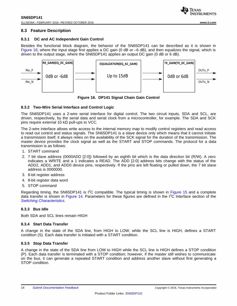
8.3 Feature Description
8.3.1 DC and AC Independent Gain ControlBesides the functional block diagram, the behavior of the SN65DP141 can be described as it is shown inFigure 16; where the input stage first applies a DC gain (0 dB or –6 dB), and then equalizes the signal, which isdriven to the output stage, where the SN65DP141 applies an output DC gain (0 dB or 6 dB).
Figure 16. DP141 Signal Chain Gain Control
8.3.2 Two-Wire Serial Interface and Control LogicThe SN65DP141 uses a 2-wire serial interface for digital control. The two circuit inputs, SDA and SCL, aredriven, respectively, by the serial data and serial clock from a microcontroller, for example. The SDA and SCKpins require external 10 kΩ pull-ups to VCC.
The 2-wire interface allows write access to the internal memory map to modify control registers and read accessto read out control and status signals. The SN65DP141 is a slave device only which means that it cannot initiatea transmission itself; it always relies on the availability of the SCK signal for the duration of the transmission. Themaster device provides the clock signal as well as the START and STOP commands. The protocol for a datatransmission is as follows:1. START command2. 7 bit slave address (0000ADD [2:0]) followed by an eighth bit which is the data direction bit (R/W). A zero
indicates a WRITE and a 1 indicates a READ. The ADD [2:0] address bits change with the status of theADD2, ADD1, and ADD0 device pins, respectively. If the pins are left floating or pulled down, the 7 bit slaveaddress is 0000000.
3. 8-bit register address4. 8-bit register data word5. STOP command
Regarding timing, the SN65DP141 is I2C compatible. The typical timing is shown in Figure 15 and a completedata transfer is shown in Figure 14. Parameters for these figures are defined in the I2C Interface section of theSwitching Characteristics.
8.3.3 Bus IdleBoth SDA and SCL lines remain HIGH
8.3.4 Start Data TransferA change in the state of the SDA line, from HIGH to LOW, while the SCL line is HIGH, defines a STARTcondition (S). Each data transfer is initiated with a START condition.
8.3.5 Stop Data TransferA change in the state of the SDA line from LOW to HIGH while the SCL line is HIGH defines a STOP condition(P). Each data transfer is terminated with a STOP condition; however, if the master still wishes to communicateon the bus, it can generate a repeated START condition and address another slave without first generating aSTOP condition.

15
SN65DP141www.ti.com SLLSES6A –FEBRUARY 2016–REVISED OCTOBER 2016
Product Folder Links: SN65DP141
Submit Documentation FeedbackCopyright © 2016, Texas Instruments Incorporated
Feature Description (continued)8.3.6 Data TransferThe number of data bytes transferred between a START and a STOP condition is not limited and is determinedby the master device. The receiver acknowledges the transfer of data.
8.3.7 AcknowledgeEach receiving device, when addressed, is obliged to generate an acknowledge bit. The transmitter releases theSDA line and a device that acknowledges must pull down the SDA line during the acknowledge clock pulse insuch a way that the SDA line is stable LOW during the HIGH period of the acknowledge clock pulse. Setup andhold times must be taken into account. When a slave-receiver doesn’t acknowledge the slave address, the dataline must be left HIGH by the slave. The master can then generate a STOP condition to abort the transfer. If theslave-receiver does acknowledge the slave address but some time later in the transfer cannot receive any moredata bytes, the master must abort the transfer. This is indicated by the slave generating the not acknowledge onthe first byte to follow. The slave leaves the data line HIGH and the master generates the STOP condition.
8.4 Device Functional Modes
8.4.1 TRACE and CABLE Equalization ModesThe SN65DP141 is optimized for both trace and cable application at its input. The device pin EQ_MODE sets theEQ gain curve profile suitable for these two use cases.
8.4.2 Control ModesThe SN65DP141 features two control modes: GPIO and I2C, and the selection between these two modes is bymeans of the I2C_EN terminal, which activates the GPIO when tied to LOW; otherwise; the I2C mode is activedue to its internal pull-up resistance.
8.4.3 GPIO MODEDevice Pins RX_GAIN, EQ1 and EQ0 determines receiver DC and AC gain as shown in Table 1 and Table 2.
Table 1. EQ Pin SettingsEQ1 EQ0 EQ SettingGND GND 000GND HiZ 000GND VCC 001HiZ GND 010HiZ HiZ 011HiZ VCC 100VCC GND 101VCC HiZ 110VCC VCC 111
Table 2. RX DC and AC GAIN SettingsEQ Configuration EQ Gain
EQ Setting RX_GAIN EQ_DC_GAIN (dB) EQ_AC_GAIN (dB)000 - 111 LOW –6 1 - 9000 - 111 HiZ –6 7 - 17000 - 111 HIGH 0 1 - 9

16
SN65DP141SLLSES6A –FEBRUARY 2016–REVISED OCTOBER 2016 www.ti.com
Product Folder Links: SN65DP141
Submit Documentation Feedback Copyright © 2016, Texas Instruments Incorporated
8.4.4 I2C Mode
Table 3. I2C Control Settings Description for RX DC and AC GAINEQ_MODE EQ_DC GAIN RX_GAIN<1:0> EQ_Setting<2:0> DC GAIN (dB) AC GAIN (dB) APPLICATION
0
000 000 to 111 –6 1 to 9 Short Input Cable; Large Input Swing
11 000 to 111 –6 7 to 17 Long Input Cable; Large Input Swing
101 000 to 111 0 1 to 9 Short Input Cable; Small Input Swing
11 000 to 111 0 2 to 10 Short Input Cable, Small Input Swing
1
000 000 to 111 –6 1 to 9 Short Input Trace; Large Input Swing
11 000 to 111 –6 7 to 17 Long Input Trace; Large Input Swing
101 000 to 111 0 1 to 9 Short Input Trace; Small Input Swing
11 000 to 111 0 2 to 10 Short Input Trace, Small Input Swing

17
SN65DP141www.ti.com SLLSES6A –FEBRUARY 2016–REVISED OCTOBER 2016
Product Folder Links: SN65DP141
Submit Documentation FeedbackCopyright © 2016, Texas Instruments Incorporated
8.5 Register Maps
8.5.1 Register 0x00 (General Device Settings) (offset = 00000000) [reset = 00000000]
Figure 17. Register 0x00 (General Device Settings)
7 6 5 4 3 2 1 0SW_GPIO PWRDOWN SYNC_01 SYNC_23 SYNC_ALL EQ_MODE RSVD
R/W R/W R/W R/W R/W R/W R/W R/WLEGEND: R/W = Read/Write; R = Read only; -n = value after reset
Table 4. Register 0x00 (General Device Settings)Bit Field Type Reset Description
7SW_GPIO R/W 0 Switching logic is controlled by GPIO or I2C:
0 = I2C control1 = GPIO control
6 PWRDOWN R/W 0 Power down the device:0 = Normal operation1 = Powerdown
5 SYNC_01 R/W 0 All settings from channel 1 will be used for channel 0 and 1:0 = Channel 0 tracking channel 1 settings1 = No tracking tracking
4 SYNC_ 23 R/W 0 All settings from channel 2 will be used for channel 2 and 3:0 = Channel 3 tracking channel 2 settings1 = No channel tracking
3 SYNC_ALL R/W 0 All settings from channel 1 will be used on all channels:0 = All channels tracking channel 11 = No channel trackingOverwrites SYNC_01 and SYNC_23
2 EQ_MODE R/W 0 Set EQ mode:0 = Cable mode1 = Trace mode
1 R/W 00 RSVD R/W 0 For TI use only
18
SN65DP141SLLSES6A –FEBRUARY 2016–REVISED OCTOBER 2016 www.ti.com
Product Folder Links: SN65DP141
Submit Documentation Feedback Copyright © 2016, Texas Instruments Incorporated
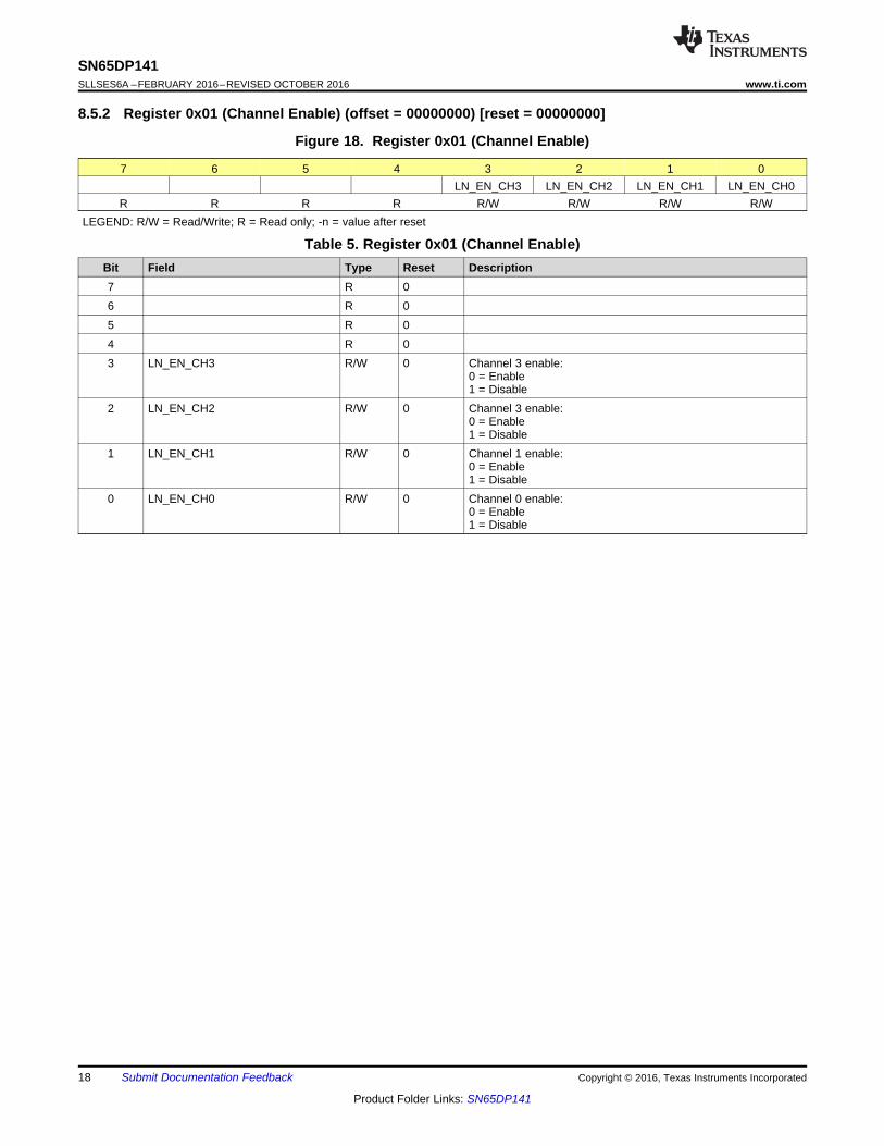
8.5.2 Register 0x01 (Channel Enable) (offset = 00000000) [reset = 00000000]
Figure 18. Register 0x01 (Channel Enable)
7 6 5 4 3 2 1 0LN_EN_CH3 LN_EN_CH2 LN_EN_CH1 LN_EN_CH0
R R R R R/W R/W R/W R/WLEGEND: R/W = Read/Write; R = Read only; -n = value after reset
Table 5. Register 0x01 (Channel Enable)Bit Field Type Reset Description7 R 06 R 05 R 04 R 03 LN_EN_CH3 R/W 0 Channel 3 enable:
0 = Enable1 = Disable
2 LN_EN_CH2 R/W 0 Channel 3 enable:0 = Enable1 = Disable
1 LN_EN_CH1 R/W 0 Channel 1 enable:0 = Enable1 = Disable
0 LN_EN_CH0 R/W 0 Channel 0 enable:0 = Enable1 = Disable
19
SN65DP141www.ti.com SLLSES6A –FEBRUARY 2016–REVISED OCTOBER 2016
Product Folder Links: SN65DP141
Submit Documentation FeedbackCopyright © 2016, Texas Instruments Incorporated
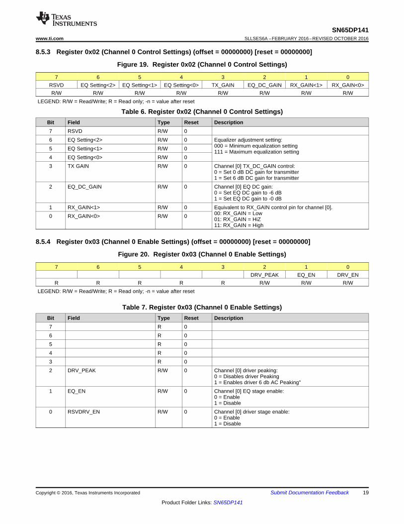
8.5.3 Register 0x02 (Channel 0 Control Settings) (offset = 00000000) [reset = 00000000]
Figure 19. Register 0x02 (Channel 0 Control Settings)
7 6 5 4 3 2 1 0RSVD EQ Setting<2> EQ Setting<1> EQ Setting<0> TX_GAIN EQ_DC_GAIN RX_GAIN<1> RX_GAIN<0>R/W R/W R/W R/W R/W R/W R/W R/W
LEGEND: R/W = Read/Write; R = Read only; -n = value after reset
Table 6. Register 0x02 (Channel 0 Control Settings)Bit Field Type Reset Description7 RSVD R/W 06 EQ Setting<2> R/W 0 Equalizer adjustment setting:
000 = Minimum equalization setting111 = Maximum equalization setting5 EQ Setting<1> R/W 0
4 EQ Setting<0> R/W 03 TX GAIN R/W 0 Channel [0] TX_DC_GAIN control:
0 = Set 0 dB DC gain for transmitter1 = Set 6 dB DC gain for transmitter
2 EQ_DC_GAIN R/W 0 Channel [0] EQ DC gain:0 = Set EQ DC gain to -6 dB1 = Set EQ DC gain to -0 dB
1 RX_GAIN<1> R/W 0 Equivalent to RX_GAIN control pin for channel [0].00: RX_GAIN = Low01: RX_GAIN = HiZ11: RX_GAIN = High
0 RX_GAIN<0> R/W 0
8.5.4 Register 0x03 (Channel 0 Enable Settings) (offset = 00000000) [reset = 00000000]
Figure 20. Register 0x03 (Channel 0 Enable Settings)
7 6 5 4 3 2 1 0DRV_PEAK EQ_EN DRV_EN
R R R R R R/W R/W R/WLEGEND: R/W = Read/Write; R = Read only; -n = value after reset
Table 7. Register 0x03 (Channel 0 Enable Settings)Bit Field Type Reset Description7 R 06 R 05 R 04 R 03 R 02 DRV_PEAK R/W 0 Channel [0] driver peaking:
0 = Disables driver Peaking1 = Enables driver 6 db AC Peaking"
1 EQ_EN R/W 0 Channel [0] EQ stage enable:0 = Enable1 = Disable
0 RSVDRV_EN R/W 0 Channel [0] driver stage enable:0 = Enable1 = Disable

20
SN65DP141SLLSES6A –FEBRUARY 2016–REVISED OCTOBER 2016 www.ti.com
Product Folder Links: SN65DP141
Submit Documentation Feedback Copyright © 2016, Texas Instruments Incorporated
8.5.5 Register 0x05 (Channel 1 Control Settings) (offset = 00000000) [reset = 00000000]
Figure 21. Register 0x05 (Channel 1 Control Settings)
7 6 5 4 3 2 1 0RSVD EQ Setting<2> EQ Setting<1> EQ Setting<0> TX_GAIN EQ_DC_GAIN RX_GAIN<1> RX_GAIN<0>R/W R/W R/W R/W R/W R/W R/W R/W
LEGEND: R/W = Read/Write; R = Read only; -n = value after reset
Table 8. Register 0x05 (Channel 1 Control Settings)Bit Field Type Reset Description7 RSVD R/W 06 EQ Setting<2> R/W 0 Equalizer adjustment setting:
000 = Minimum equalization setting111 = Maximum equalization setting5 EQ Setting<1> R/W 0
4 EQ Setting<0> R/W 03 TX_GAIN R/W 0 Channel [1] TX_DC_GAIN control:
0 = Set 0 dB DC gain for transmitter1 = Set 6 dB DC gain for transmitter
2 EQ_DC_GAIN R/W 0 Channel [1] EQ DC gain:0 = Set EQ DC gain to -6 dB1 = Set EQ DC gain to -0 dB
1 RX_GAIN<1> R/W 0 Equivalent to RX_GAIN control pin for channel [1].00: RX_GAIN = Low01: RX_GAIN = HiZ11: RX_GAIN = High
0 RX_GAIN<0> R/W 0
8.5.6 Register 0x06 (Channel 1 Enable Settings) (offset = 00000000) [reset = 00000000]
Figure 22. Register 0x06 (Channel 1 Enable Settings)
7 6 5 4 3 2 1 0DRV_PEAK EQ_EN DRV_EN
R R R R R R/W R/W R/WLEGEND: R/W = Read/Write; R = Read only; -n = value after reset
Table 9. Register 0x06 (Channel 1 Enable Settings)Bit Field Type Reset Description7 R 06 R 05 R 04 R 03 R 02 DRV_PEAK R/W 0 Channel [1] driver peaking:
0 = Disables driver Peaking1 = Enables driver 6 db AC Peaking
1 EQ_EN R/W 0 Channel [1] EQ stage enable:0 = Enable1 = Disable
0 DRV_EN R/W 0 Channel [1] driver stage enable:0 = Enable1 = Disable

21
SN65DP141www.ti.com SLLSES6A –FEBRUARY 2016–REVISED OCTOBER 2016
Product Folder Links: SN65DP141
Submit Documentation FeedbackCopyright © 2016, Texas Instruments Incorporated
8.5.7 Register 0x08 (Channel 2 Control Settings) (offset = 00000000) [reset = 00000000]
Figure 23. Register 0x08 (Channel 2 Control Settings)
7 6 5 4 3 2 1 0RSVD EQ Setting<2> EQ Setting<1> EQ Setting<0> TX_GAIN EQ_DC_GAIN RX_GAIN<1> RX_GAIN<0>R/W R/W R/W R/W R/W R/W R/W R/W
LEGEND: R/W = Read/Write; R = Read only; -n = value after reset
Table 10. Register 0x08 (Channel 2 Control Settings)Bit Field Type Reset Description7 RSVD R/W 06 EQ Setting<2> R/W 0 Equalizer adjustment setting:
000 = Minimum equalization setting111 = Maximum equalization setting5 EQ Setting<1> R/W 0
4 EQ Setting<0> R/W 03 TX_GAIN R/W 0 Channel [2] TX_DC_GAIN control:
0 = Set 0 dB DC gain for transmitter1 = Set 6 dB DC gain for transmitter
2 EQ_DC_GAIN R/W 0 Channel [2] EQ DC gain:0 = Set EQ DC gain to -6 dB1 = Set EQ DC gain to -0 dB
1 RX_GAIN<1> R/W 0 Equivalent to RX_GAIN control pin for channel [2].00: RX_GAIN = Low01: RX_GAIN = HiZ11: RX_GAIN = High
0 RX_GAIN<0> R/W 0
8.5.8 Register 0x09 (Channel 2 Enable Settings) (offset = 00000000) [reset = 00000000]
Figure 24. Register 0x09 (Channel 2 Enable Settings)
7 6 5 4 3 2 1 0DRV_PEAK EQ_EN DRV_EN
R R R R R R/W R/W R/WLEGEND: R/W = Read/Write; R = Read only; -n = value after reset
Table 11. Register 0x09 (Channel 2 Enable Settings)Bit Field Type Reset Description7 R 06 R 05 R 04 R 03 R 02 DRV_PEAK R/W 0 Channel [2] driver peaking:
0 = Disables driver Peaking1 = Enables driver 6 db AC Peaking
1 EQ_EN R/W 0 Channel [2] driver stage enable:0 = Enable1 = Disable
0 DRV_EN R/W 0 Channel [2] driver stage enable:0 = Enable1 = Disable

22
SN65DP141SLLSES6A –FEBRUARY 2016–REVISED OCTOBER 2016 www.ti.com
Product Folder Links: SN65DP141
Submit Documentation Feedback Copyright © 2016, Texas Instruments Incorporated
8.5.9 Register 0x0B (Channel 3 Control Settings) (offset = 00000000) [reset = 00000000]
Figure 25. Register 0x0B (Channel 3 Control Settings)
7 6 5 4 3 2 1 0RSVD EQ Setting<2> EQ Setting<1> EQ Setting<0> TX_GAIN EQ_DC_GAIN RX_GAIN<1> RX_GAIN<0>R/W R/W R/W R/W R/W R/W R/W R/W
LEGEND: R/W = Read/Write; R = Read only; -n = value after reset
Table 12. Register 0x0B (Channel 3 Control Settings)Bit Field Type Reset Description7 RSVD R/W 06 EQ Setting<2> R/W 0 Equalizer adjustment setting:
000 = Minimum equalization setting111 = Maximum equalization setting5 EQ Setting<1> R/W 0
4 EQ Setting<0> R/W 03 TX_GAIN R/W 0 Channel [3] TX_DC_GAIN control:
0 = Set 0 dB DC gain for transmitter1 = Set 6 dB DC gain for transmitter
2 EQ_DC_GAIN R/W 0 Channel [3] EQ DC gain:0 = Set EQ DC gain to -6 dB1 = Set EQ DC gain to -0 dB
1 RX_GAIN<1> R/W 0 Equivalent to RX_GAIN control pin for channel [3].00: RX_GAIN = Low01: RX_GAIN = HiZ11: RX_GAIN = High
0 RX_GAIN<0> R/W 0
8.5.10 Register 0x0C (Channel 3 Control Settings) (offset = 00000000) [reset = 00000000]
Figure 26. Register 0x0C (Channel 3 Enable Settings)
7 6 5 4 3 2 1 0DRV_PEAK EQ_EN DRV_EN
R R R R R R/W R/W R/WLEGEND: R/W = Read/Write; R = Read only; -n = value after reset
Table 13. Register 0x0C (Channel 3 Enable Settings)Bit Field Type Reset Description7 R 06 R 05 R 04 R 03 R 02 DRV_PEAK R/W 0 Channel [3] driver peaking:
0 = Disables driver Peaking1 = Enables driver 6db AC Peaking
1 EQ_EN R/W 0 Channel [3] EQ stage enable:0 = Enable1 = Disable
0 RSVDRV_EN R/W 0 Channel [3] driver stage enable:0 = Enable1 = Disable
POWER SOURCE 3P3V
DP SOURCE DP SINK
ML0_IN
ML1_IN
ML2_IN
ML3_INDP141
ML0_OUT
ML1_OUT
ML2_OUT
ML3_OUT
3P3V
AUX
HPD
Copyright © 2016, Texas Instruments Incorporated
23
SN65DP141www.ti.com SLLSES6A –FEBRUARY 2016–REVISED OCTOBER 2016
Product Folder Links: SN65DP141
Submit Documentation FeedbackCopyright © 2016, Texas Instruments Incorporated
9 Application and Implementation
NOTEInformation in the following applications sections is not part of the TI componentspecification, and TI does not warrant its accuracy or completeness. TI’s customers areresponsible for determining suitability of components for their purposes. Customers shouldvalidate and test their design implementation to confirm system functionality.
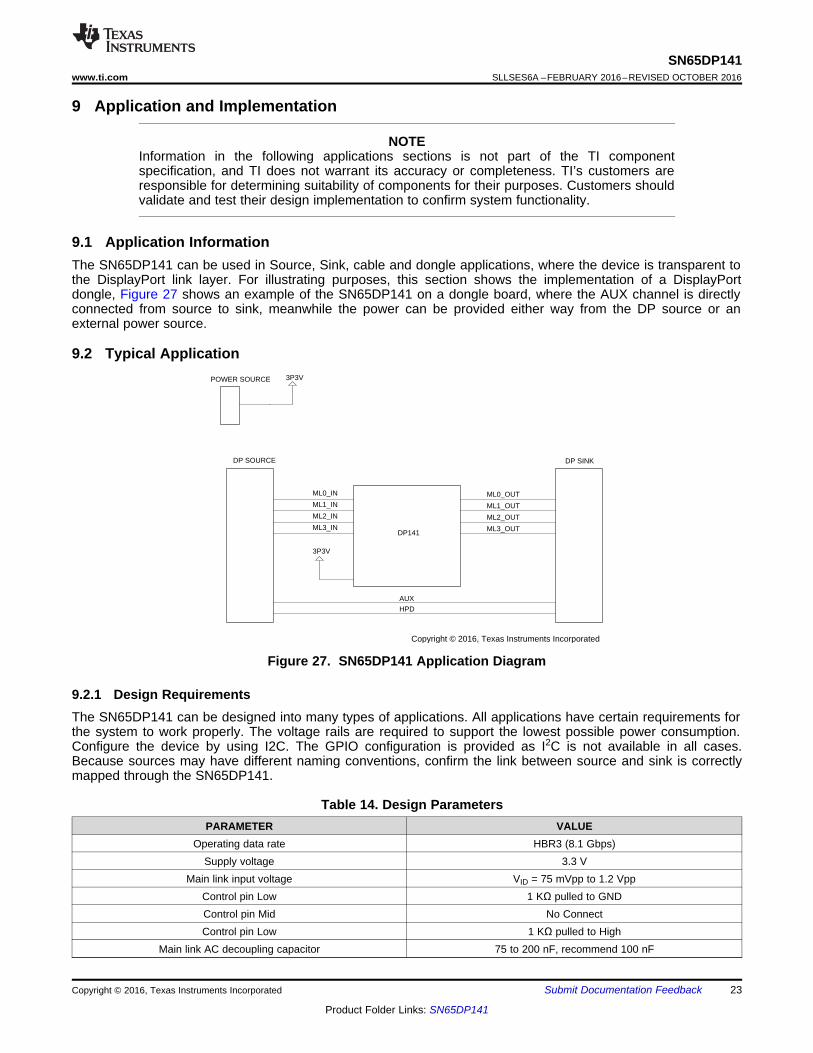
9.1 Application InformationThe SN65DP141 can be used in Source, Sink, cable and dongle applications, where the device is transparent tothe DisplayPort link layer. For illustrating purposes, this section shows the implementation of a DisplayPortdongle, Figure 27 shows an example of the SN65DP141 on a dongle board, where the AUX channel is directlyconnected from source to sink, meanwhile the power can be provided either way from the DP source or anexternal power source.
9.2 Typical Application
Figure 27. SN65DP141 Application Diagram
9.2.1 Design RequirementsThe SN65DP141 can be designed into many types of applications. All applications have certain requirements forthe system to work properly. The voltage rails are required to support the lowest possible power consumption.Configure the device by using I2C. The GPIO configuration is provided as I2C is not available in all cases.Because sources may have different naming conventions, confirm the link between source and sink is correctlymapped through the SN65DP141.
Table 14. Design ParametersPARAMETER VALUE
Operating data rate HBR3 (8.1 Gbps)Supply voltage 3.3 V
Main link input voltage VID = 75 mVpp to 1.2 VppControl pin Low 1 KΩ pulled to GNDControl pin Mid No ConnectControl pin Low 1 KΩ pulled to High
Main link AC decoupling capacitor 75 to 200 nF, recommend 100 nF

Place near DP141
NOTE:Min of 15 Viasrecommended for GND Padconnection
EN
SILKSCREEN:
Device disable/I2C Reset if asserted low
Value of the cap to varydepending on power railramp-up time
NOTE: ALL DIFF PAIRS AREROUTEDTO 90 OHMSDIFFERENTIAL AND 50 OHMSCOMMON MODE. ALL OTHERTRACES ARE 50 OHM.
Connecting to DP Receiver
141_DP_IN0P141_DP_IN0N
141_DP_IN1P141_DP_IN1N
141_DP_IN2P141_DP_IN2N
141_DP_IN3P141_DP_IN3N
141_DP_OUT0P141_DP_OUT0N
141_DP_OUT1P141_DP_OUT1N
141_DP_OUT2P141_DP_OUT2N
141_DP_OUT3P141_DP_OUT3N
SDA
SDADRV_PK#/SCLI2C_EN
VOD/CS
EQ0/ADD0EQ1/ADD1
EQ_MODE/ADD2PWD#
PWD#
SNK_DP_ML0P
SNK_DP_ML0N
SNK_DP_ML1P
SNK_DP_ML1N
SNK_DP_ML2P
SNK_DP_ML2N
SNK_DP_ML3P
SNK_DP_ML3N
DRV_PK#/SCL I2C_EN VOD/CS EQ0/ADD0 EQ1/ADD1 EQ_MODE/ADD2
SDA
DRV_PK#/SCL
3P3V
3P3V
3P3V
3P3V
BOARD_3P3V BOARD_3P3V BOARD_3P3V BOARD_3P3VBOARD_3P3V
BOARD_3P3V
BOARD_3P3V
BOARD_3P3V
SRC_DP_ML0P
SRC_DP_ML0N
SRC_DP_ML1P
SRC_DP_ML1N
SRC_DP_ML2P
SRC_DP_ML2N
SRC_DP_ML3P
SRC_DP_ML3N
SNK_DP_ML0P
SNK_DP_ML0N
SNK_DP_ML1P
SNK_DP_ML1N
SNK_DP_ML2P
SNK_DP_ML2N
SNK_DP_ML3P
R18
0R
R11DNI, 1K
U1
IN0_P1
IN0_N2
VC
C3
IN1_P4
IN1_N5
VC
C6
VC
C7
IN2_P8
IN2_N9
VC
C10
IN3_P11
IN3_N12
VC
C13
REXT18
VC
C19
OUT3_N20OUT3_P21
VC
C22
OUT2_N23OUT2_P24
VC
C25
VC
C26
OUT1_N27OUT1_P28
VC
C29
OUT0_N30OUT0_P31V
CC
32
EQ0/ADD033
EQ1/ADD134
EQ_MODE/ADD235
GAIN36
PWD#37
VC
C38
VOD/CS17
DRV_PK#/SCL15 SDA14
I2C_EN16
PwPd39
R31K
R7DNI, 1K
C27 0.1uF0201
LP1
SW1B3SN-3012
1 4
2 3
C12 0.1uF0201
FB1
220 @ 100MHZ
C2
0.1uFLP2
C15 0.1uF0201
R15DNI, 1K
R10
1K
C281uF
C3
0.1uF
J8
Header 5x2 0.1" Shroud RA thru-hole
246810
13579
C18 0.1uF0201
R13DNI, 1K
C16 0.1uF0201
C4
0.1uF
C14 0.1uF0201
C10
0.1uF
J5
HDR3X1 M .1
123
C13 0.1uF0201
J3
HDR3X1 M .1
123
C20 0.1uF0201
R16DNI, 1K
C5
0.1uF
R1
1.2K
C17 0.1uF0201
R8DNI, 1K
J2
HDR3X1 M .1
123
C11
0.1uF
C22 0.1uF0201
C6
0.1uF
R6DNI, 1K
R9DNI, 1K
C19 0.1uF0201
C24 0.1uF0201
C7
0.1uF
R12DNI, 1K
C21 0.1uF0201
J6
HDR3X1 M .1
123
C8
0.1uF
R5DNI, 1K
C1
10uF
R2
1K
J4
HDR3X1 M .1
123
J1
HDR3X1 M .1
123
C26 0.1uF0201
C25 0.1uF0201
R4DNI, 1K
R14DNI, 1K
C9
0.1uF
C23 0.1uF0201
DP_PWRDP_PWR_SRC
BOARD_3P3V
5V
5V
BOARD_3P3V
C30
22uF
R28 175K
U2
TPS62082DSGT
VIN8
EN1
MODE3
GND2
Pw
Pd
9
FB4
VOS5
SW7
PG
6
J13
USB2_micAB_Recept
VBUS1
D-2
D+3
ID4
GND5
Shield16
Shield27
Shield38
Shield49
Shield510
Shield611
C29
10uF
J12
HDR3X1 M .1
123
L1
1uH
SNK_DP_ML3N
J0
HDR3X1 M .1
123
DP141
24
SN65DP141SLLSES6A –FEBRUARY 2016–REVISED OCTOBER 2016 www.ti.com
Product Folder Links: SN65DP141
Submit Documentation Feedback Copyright © 2016, Texas Instruments Incorporated
First approach for GAIN configuration: It is highly recommend that DC GAIN be set to 1, this leads the output topreserve the input amplitude (GAIN = 1):• For GPIO implementation: Use a pull-up resistor on the GAIN terminal (pin 36), refer to the schematic in
Figure 28.• For I2C implementation: write a 1 to the bit 2 of the registers 0x02, 0x05, 0x08 and 0x0B. Refer to Two-Wire
Serial Interface and Control Logic for a detailed description of the I2C interface
9.2.2 Detailed Design ProcedureDesigning in the SN65DP141 requires the following:• Determine the loss profile on the DP input and output channels and cables.• Based upon the loss profile and signal swing, determine the optimal configuration for the SN65DP141, to
pass electrical compliance (Equalization mode, EQ Gain, DC gain, AC Gain).• See Figure 28 for information on using the AC coupling capacitors and control pin resistors, as well as for
recommended decouple capacitors from VCC pins to ground.• Configure the TheSN65DP141 using the GPIO terminals or the I2C interface:
– GPIO – Using the terminals EQ_MODE, EQ1, EQ1 and gain.– I2C – Refer to the I2C Register Maps and the Two-Wire Serial Interface and Control Logic sections for a
detailed configuration procedures.• The thermal pad must be connected to ground.
Figure 28. SN65DP141 Application Schematic
0
0.05
0.1
0.15
0.2
0.25
0.3
0.35
0 200 400 600 800 1k 1k 1k 2k 2k 2kTime (ps)
Am
plitu
de (
mV
)
3 meter6 meter6 meter (See Note A)
G008
−50
−45
−40
−35
−30
−25
−20
−15
−10
−5
0
0 2 4 6 8 10Frequency (GHz)
Mag
nitu
de (
dB)
3 meter6 meter6 meter (See Note A)
G009
0
0.05
0.1
0.15
0.2
0.25
0 200 400 600 800 1k 1.2k 1.4k 1.6k 1.8k 2kTime (ps)
Am
plitu
de (
mV
)
3 meter6 meter6 meter (See Note A)
G006
−45
−40
−35
−30
−25
−20
−15
−10
−5
0
0 2 4 6 8 10Frequency (GHz)
Mag
nitu
de (
dB)
3 meter6 meter6 meter (See Note A)
G007
25
SN65DP141www.ti.com SLLSES6A –FEBRUARY 2016–REVISED OCTOBER 2016
Product Folder Links: SN65DP141
Submit Documentation FeedbackCopyright © 2016, Texas Instruments Incorporated
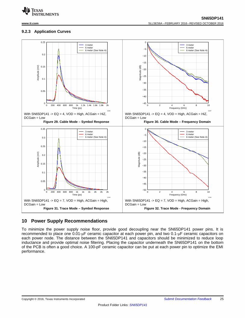
9.2.3 Application Curves
With SN65DP141 -> EQ = 4, VOD = High, ACGain = HiZ,DCGain = Low
Figure 29. Cable Mode – Symbol Response
With SN65DP141 -> EQ = 4, VOD = High, ACGain = HiZ,DCGain = Low
Figure 30. Cable Mode – Frequency Domain
With SN65DP141 -> EQ = 7, VOD = High, ACGain = High,DCGain = Low
Figure 31. Trace Mode – Symbol Response
With SN65DP141 -> EQ = 7, VOD = High, ACGain = High,DCGain = Low
Figure 32. Trace Mode - Frequency Domain
10 Power Supply RecommendationsTo minimize the power supply noise floor, provide good decoupling near the SN65DP141 power pins. It isrecommended to place one 0.01-μF ceramic capacitor at each power pin, and two 0.1-μF ceramic capacitors oneach power node. The distance between the SN65DP141 and capacitors should be minimized to reduce loopinductance and provide optimal noise filtering. Placing the capacitor underneath the SN65DP141 on the bottomof the PCB is often a good choice. A 100-pF ceramic capacitor can be put at each power pin to optimize the EMIperformance.
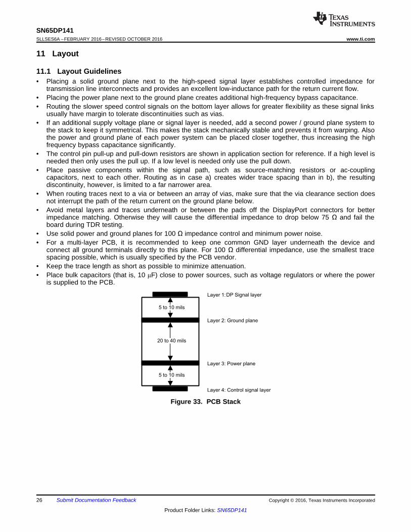
Layer 1:
Layer 2: Ground plane
Layer 3: Power plane
Layer 4: Control signal layer
5 to 10 mils
20 to 40 mils
5 to 10 mils
DP Signal layer
26
SN65DP141SLLSES6A –FEBRUARY 2016–REVISED OCTOBER 2016 www.ti.com
Product Folder Links: SN65DP141
Submit Documentation Feedback Copyright © 2016, Texas Instruments Incorporated
11 Layout
11.1 Layout Guidelines• Placing a solid ground plane next to the high-speed signal layer establishes controlled impedance for
transmission line interconnects and provides an excellent low-inductance path for the return current flow.• Placing the power plane next to the ground plane creates additional high-frequency bypass capacitance.• Routing the slower speed control signals on the bottom layer allows for greater flexibility as these signal links
usually have margin to tolerate discontinuities such as vias.• If an additional supply voltage plane or signal layer is needed, add a second power / ground plane system to
the stack to keep it symmetrical. This makes the stack mechanically stable and prevents it from warping. Alsothe power and ground plane of each power system can be placed closer together, thus increasing the highfrequency bypass capacitance significantly.
• The control pin pull-up and pull-down resistors are shown in application section for reference. If a high level isneeded then only uses the pull up. If a low level is needed only use the pull down.
• Place passive components within the signal path, such as source-matching resistors or ac-couplingcapacitors, next to each other. Routing as in case a) creates wider trace spacing than in b), the resultingdiscontinuity, however, is limited to a far narrower area.
• When routing traces next to a via or between an array of vias, make sure that the via clearance section doesnot interrupt the path of the return current on the ground plane below.
• Avoid metal layers and traces underneath or between the pads off the DisplayPort connectors for betterimpedance matching. Otherwise they will cause the differential impedance to drop below 75 Ω and fail theboard during TDR testing.
• Use solid power and ground planes for 100 Ω impedance control and minimum power noise.• For a multi-layer PCB, it is recommended to keep one common GND layer underneath the device and
connect all ground terminals directly to this plane. For 100 Ω differential impedance, use the smallest tracespacing possible, which is usually specified by the PCB vendor.
• Keep the trace length as short as possible to minimize attenuation.• Place bulk capacitors (that is, 10 μF) close to power sources, such as voltage regulators or where the power
is supplied to the PCB.
Figure 33. PCB Stack

27
SN65DP141www.ti.com SLLSES6A –FEBRUARY 2016–REVISED OCTOBER 2016
Product Folder Links: SN65DP141
Submit Documentation FeedbackCopyright © 2016, Texas Instruments Incorporated
11.2 Layout Example
Figure 34. Example Layout (Top)
Figure 35. Example Layout (Top)

28
SN65DP141SLLSES6A –FEBRUARY 2016–REVISED OCTOBER 2016 www.ti.com
Product Folder Links: SN65DP141
Submit Documentation Feedback Copyright © 2016, Texas Instruments Incorporated
12 Device and Documentation Support
12.1 Receiving Notification of Documentation UpdatesTo receive notification of documentation updates, navigate to the device product folder on ti.com. In the upperright corner, click on Alert me to register and receive a weekly digest of any product information that haschanged. For change details, review the revision history included in any revised document.
12.2 Community ResourcesThe following links connect to TI community resources. Linked contents are provided "AS IS" by the respectivecontributors. They do not constitute TI specifications and do not necessarily reflect TI's views; see TI's Terms ofUse.
TI E2E™ Online Community TI's Engineer-to-Engineer (E2E) Community. Created to foster collaborationamong engineers. At e2e.ti.com, you can ask questions, share knowledge, explore ideas and helpsolve problems with fellow engineers.
Design Support TI's Design Support Quickly find helpful E2E forums along with design support tools andcontact information for technical support.
12.3 TrademarksE2E is a trademark of Texas Instruments.All other trademarks are the property of their respective owners.
12.4 Electrostatic Discharge CautionThese devices have limited built-in ESD protection. The leads should be shorted together or the device placed in conductive foamduring storage or handling to prevent electrostatic damage to the MOS gates.
12.5 GlossarySLYZ022 — TI Glossary.
This glossary lists and explains terms, acronyms, and definitions.
13 Mechanical, Packaging, and Orderable InformationThe following pages include mechanical, packaging, and orderable information. This information is the mostcurrent data available for the designated devices. This data is subject to change without notice and revision ofthis document. For browser-based versions of this data sheet, refer to the left-hand navigation.

PACKAGE OPTION ADDENDUM
www.ti.com 23-May-2016
Addendum-Page 1
PACKAGING INFORMATION
Orderable Device Status(1)
Package Type PackageDrawing
Pins PackageQty
Eco Plan(2)
Lead/Ball Finish(6)
MSL Peak Temp(3)
Op Temp (°C) Device Marking(4/5)
Samples
SN65DP141RLJR ACTIVE WQFN RLJ 38 3000 Green (RoHS& no Sb/Br)
CU NIPDAU Level-3-260C-168 HR -40 to 85 DP141
SN65DP141RLJT ACTIVE WQFN RLJ 38 250 Green (RoHS& no Sb/Br)
CU NIPDAU Level-3-260C-168 HR -40 to 85 DP141
(1) The marketing status values are defined as follows:ACTIVE: Product device recommended for new designs.LIFEBUY: TI has announced that the device will be discontinued, and a lifetime-buy period is in effect.NRND: Not recommended for new designs. Device is in production to support existing customers, but TI does not recommend using this part in a new design.PREVIEW: Device has been announced but is not in production. Samples may or may not be available.OBSOLETE: TI has discontinued the production of the device.
(2) Eco Plan - The planned eco-friendly classification: Pb-Free (RoHS), Pb-Free (RoHS Exempt), or Green (RoHS & no Sb/Br) - please check http://www.ti.com/productcontent for the latest availabilityinformation and additional product content details.TBD: The Pb-Free/Green conversion plan has not been defined.Pb-Free (RoHS): TI's terms "Lead-Free" or "Pb-Free" mean semiconductor products that are compatible with the current RoHS requirements for all 6 substances, including the requirement thatlead not exceed 0.1% by weight in homogeneous materials. Where designed to be soldered at high temperatures, TI Pb-Free products are suitable for use in specified lead-free processes.Pb-Free (RoHS Exempt): This component has a RoHS exemption for either 1) lead-based flip-chip solder bumps used between the die and package, or 2) lead-based die adhesive used betweenthe die and leadframe. The component is otherwise considered Pb-Free (RoHS compatible) as defined above.Green (RoHS & no Sb/Br): TI defines "Green" to mean Pb-Free (RoHS compatible), and free of Bromine (Br) and Antimony (Sb) based flame retardants (Br or Sb do not exceed 0.1% by weightin homogeneous material)
(3) MSL, Peak Temp. - The Moisture Sensitivity Level rating according to the JEDEC industry standard classifications, and peak solder temperature.
(4) There may be additional marking, which relates to the logo, the lot trace code information, or the environmental category on the device.
(5) Multiple Device Markings will be inside parentheses. Only one Device Marking contained in parentheses and separated by a "~" will appear on a device. If a line is indented then it is a continuationof the previous line and the two combined represent the entire Device Marking for that device.
(6) Lead/Ball Finish - Orderable Devices may have multiple material finish options. Finish options are separated by a vertical ruled line. Lead/Ball Finish values may wrap to two lines if the finishvalue exceeds the maximum column width.
Important Information and Disclaimer:The information provided on this page represents TI's knowledge and belief as of the date that it is provided. TI bases its knowledge and belief on informationprovided by third parties, and makes no representation or warranty as to the accuracy of such information. Efforts are underway to better integrate information from third parties. TI has taken andcontinues to take reasonable steps to provide representative and accurate information but may not have conducted destructive testing or chemical analysis on incoming materials and chemicals.TI and TI suppliers consider certain information to be proprietary, and thus CAS numbers and other limited information may not be available for release.

PACKAGE OPTION ADDENDUM
www.ti.com 23-May-2016
Addendum-Page 2
In no event shall TI's liability arising out of such information exceed the total purchase price of the TI part(s) at issue in this document sold by TI to Customer on an annual basis.

TAPE AND REEL INFORMATION
*All dimensions are nominal
Device PackageType
PackageDrawing
Pins SPQ ReelDiameter
(mm)
ReelWidth
W1 (mm)
A0(mm)
B0(mm)
K0(mm)
P1(mm)
W(mm)
Pin1Quadrant
SN65DP141RLJR WQFN RLJ 38 3000 330.0 16.4 5.25 7.25 1.45 8.0 16.0 Q1
SN65DP141RLJT WQFN RLJ 38 250 330.0 16.4 5.25 7.25 1.45 8.0 16.0 Q1
PACKAGE MATERIALS INFORMATION
www.ti.com 23-May-2016
Pack Materials-Page 1

*All dimensions are nominal
Device Package Type Package Drawing Pins SPQ Length (mm) Width (mm) Height (mm)
SN65DP141RLJR WQFN RLJ 38 3000 367.0 367.0 38.0
SN65DP141RLJT WQFN RLJ 38 250 367.0 367.0 38.0
PACKAGE MATERIALS INFORMATION
www.ti.com 23-May-2016
Pack Materials-Page 2


IMPORTANT NOTICE
Texas Instruments Incorporated and its subsidiaries (TI) reserve the right to make corrections, enhancements, improvements and otherchanges to its semiconductor products and services per JESD46, latest issue, and to discontinue any product or service per JESD48, latestissue. Buyers should obtain the latest relevant information before placing orders and should verify that such information is current andcomplete. All semiconductor products (also referred to herein as “components”) are sold subject to TI’s terms and conditions of salesupplied at the time of order acknowledgment.TI warrants performance of its components to the specifications applicable at the time of sale, in accordance with the warranty in TI’s termsand conditions of sale of semiconductor products. Testing and other quality control techniques are used to the extent TI deems necessaryto support this warranty. Except where mandated by applicable law, testing of all parameters of each component is not necessarilyperformed.TI assumes no liability for applications assistance or the design of Buyers’ products. Buyers are responsible for their products andapplications using TI components. To minimize the risks associated with Buyers’ products and applications, Buyers should provideadequate design and operating safeguards.TI does not warrant or represent that any license, either express or implied, is granted under any patent right, copyright, mask work right, orother intellectual property right relating to any combination, machine, or process in which TI components or services are used. Informationpublished by TI regarding third-party products or services does not constitute a license to use such products or services or a warranty orendorsement thereof. Use of such information may require a license from a third party under the patents or other intellectual property of thethird party, or a license from TI under the patents or other intellectual property of TI.Reproduction of significant portions of TI information in TI data books or data sheets is permissible only if reproduction is without alterationand is accompanied by all associated warranties, conditions, limitations, and notices. TI is not responsible or liable for such altereddocumentation. Information of third parties may be subject to additional restrictions.Resale of TI components or services with statements different from or beyond the parameters stated by TI for that component or servicevoids all express and any implied warranties for the associated TI component or service and is an unfair and deceptive business practice.TI is not responsible or liable for any such statements.Buyer acknowledges and agrees that it is solely responsible for compliance with all legal, regulatory and safety-related requirementsconcerning its products, and any use of TI components in its applications, notwithstanding any applications-related information or supportthat may be provided by TI. Buyer represents and agrees that it has all the necessary expertise to create and implement safeguards whichanticipate dangerous consequences of failures, monitor failures and their consequences, lessen the likelihood of failures that might causeharm and take appropriate remedial actions. Buyer will fully indemnify TI and its representatives against any damages arising out of the useof any TI components in safety-critical applications.In some cases, TI components may be promoted specifically to facilitate safety-related applications. With such components, TI’s goal is tohelp enable customers to design and create their own end-product solutions that meet applicable functional safety standards andrequirements. Nonetheless, such components are subject to these terms.No TI components are authorized for use in FDA Class III (or similar life-critical medical equipment) unless authorized officers of the partieshave executed a special agreement specifically governing such use.Only those TI components which TI has specifically designated as military grade or “enhanced plastic” are designed and intended for use inmilitary/aerospace applications or environments. Buyer acknowledges and agrees that any military or aerospace use of TI componentswhich have not been so designated is solely at the Buyer's risk, and that Buyer is solely responsible for compliance with all legal andregulatory requirements in connection with such use.TI has specifically designated certain components as meeting ISO/TS16949 requirements, mainly for automotive use. In any case of use ofnon-designated products, TI will not be responsible for any failure to meet ISO/TS16949.
Products ApplicationsAudio www.ti.com/audio Automotive and Transportation www.ti.com/automotiveAmplifiers amplifier.ti.com Communications and Telecom www.ti.com/communicationsData Converters dataconverter.ti.com Computers and Peripherals www.ti.com/computersDLP® Products www.dlp.com Consumer Electronics www.ti.com/consumer-appsDSP dsp.ti.com Energy and Lighting www.ti.com/energyClocks and Timers www.ti.com/clocks Industrial www.ti.com/industrialInterface interface.ti.com Medical www.ti.com/medicalLogic logic.ti.com Security www.ti.com/securityPower Mgmt power.ti.com Space, Avionics and Defense www.ti.com/space-avionics-defenseMicrocontrollers microcontroller.ti.com Video and Imaging www.ti.com/videoRFID www.ti-rfid.comOMAP Applications Processors www.ti.com/omap TI E2E Community e2e.ti.comWireless Connectivity www.ti.com/wirelessconnectivity
Mailing Address: Texas Instruments, Post Office Box 655303, Dallas, Texas 75265Copyright © 2016, Texas Instruments Incorporated
Recommended