1
Size effects in the thermal conductivity of gallium oxide (-Ga2O3) films grown via open-
atmosphere annealing of gallium nitride (GaN)
Chester Szwejkowski,1 Nicole Creange,2 Kai Sun,3 Ashutosh Giri,1
Brian Donovan,1 Costel Constantin,2,a Patrick E. Hopkins1,b
1. Department of Mechanical and Aerospace Engineering,
University of Virginia, Charlottesville, VA, USA 22904
2. Department of Physics and Astronomy,
James Madison University, Harrisonburg, VA, USA 22807
3. Department of Materials Science and Engineering,
University of Michigan, Ann Arbor, MI, USA 48109
a) electronic mail: [email protected]
b) electronic mail: [email protected]

2
Abstract: Gallium nitride (GaN) is a widely used semiconductor for high frequency and high
power devices because of its unique electrical properties; a wide band gap, high breakdown field,
and high electron mobility. However, thermal management has become a limiting factor regarding
efficiency, lifetime and advancement of GaN devices and GaN-based applications. In this work,
we study the thermal conductivity of beta-phase gallium oxide (β-Ga2O3) thin films, a component
of typical gate oxides used in such devices. We use time domain thermoreflectance to measure the
thermal conductivity of a variety of polycrystalline β-Ga2O3 films of different thicknesses grown
via open atmosphere annealing of the surfaces of GaN films on sapphire substrates. We show that
the effective thermal conductivity of β-Ga2O3 can span 1.5 orders of magnitude, increasing with
an increased film thickness, which is indicative of the relatively large intrinsic thermal
conductivity of bulk β-Ga2O3 (9.7 ± 2.5 W m-1 K-1) and large mean free paths compared to typical
gate dielectrics commonly used in GaN device contacts. By conducting TDTR measurements with
different metal transducers (Al, Au, and Au with a Ti wetting layer), we attribute this variation in
effective thermal conductivity to size effects in the β-Ga2O3 film resulting from phonon scattering
at the β-Ga2O3/GaN interface. From our measurements, we quantify the thermal boundary
conductance across the β-Ga2O3/GaN interface as 31.2 ± 8.1 MW m-2 K-1, in the range of typical
thermal boundary conductances previously observed non-metal/non-metal interfaces. The
measured thermal properties of open atmosphere-grown β-Ga2O3 and its interface with GaN set
the stage for thermal engineering of gate contacts in high frequency GaN-based devices.
Keywords: gallium nitride, gallium oxide, roughness, gate oxide, thermal conductivity, thermal
boundary conductance, open atmosphere annealing
I. INTRODUCTION
3
As the characteristic times and lengths of devices decrease to scales on the order of the
carrier scattering rates and mean free paths, thermal management of material boundaries can
become a critical aspect of design.1-3 In this regime, the energy transport mechanisms that are
intrinsic to the materials comprising the device can contribute much less to the overall thermal
resistance of the system as compared to the resistances across the individual interfaces. The
efficacy of transmitting energy across these solid interfaces can be quantified via the thermal
boundary conductance,4 or Kapitza Conductance,5 (the inverse of which is the thermal boundary
resistance or Kapitza Resistance), and is the constant of proportionality that relates the heat flux
to the temperature drop across this interfacial region, mathematically expressed as hK = q/T,
where hK is the thermal boundary conductance, q is the thermal flux, and T is the interfacial
temperature drop.4 The range of phonon-dominated thermal boundary conductances between
solids at room temperature span roughly two orders of magnitude from ~5 – 500 MW m-2 K-1, and
can be strongly related to the atomic structure and chemistry around the interface.6 To put this into
perspective, this energy transport pathway can offer the equivalent thermal resistance as roughly
300 – 3.0 nm of high quality SiO2, respectively. Given the wide spread use of thin gate oxides and
additional sacrificial layers in electronic nanodevices, the addition of this thermal resistance
associated with interfaces can be highly detrimental to device operation and reliability.
The need for interfacial thermal engineering has emerged as a particular bottleneck in
development of high power devices.7 Where the processor industry has hit roadblocks in
maintaining Moore’s Law from on chip power densities exceeding 100 W cm-2 (higher than a
typical lab hotplate),7 even greater power densities have been observed in radio frequency (RF)
amplifier gallium nitride-based (GaN) devices.8, 9 This increase in power density creates massive
hot-spots in GaN active regions, mainly concentrated near the gate contacts, which directly leads

4
to underperformance and eventual failure of these devices. This thermal bottleneck therefore
creates a major issue for furthering of GaN-based technologies, such as high-electron-mobility
transistors (HEMTs) for high frequency devices, light emitting diodes (LEDs) for energy-efficient
illumination, RADAR technologies (ship-board, airborne and ground) and high performance space
satellites.
Accordingly, engineering of the thermal properties and energy transport mechanisms
associated with the GaN gate contacts can elucidate thermal mitigation mechanisms to improve
GaN performance by reducing Joule heating effects attributed to the thermal resistance at this
junction. In a typical GaN device, such as a MOSFET, the thermal resistances associated with this
junction will consist of the metal electrode, a high-dielectric constant (“high-k”) gate oxide, the
GaN channel, and the material interfaces at each of these contacts. It is well known that typical
gate oxides can have very low thermal conductivities (~1 W m-1 K-1), and can vary greatly
depending on the deposition procedure.10-12 However, the thermal properties of β-Ga2O3, a
common gate oxide component in high frequency devices (including GaN),13-15 are relatively
unstudied. Furthermore, the effects of film thickness on the thermal properties of this oxide,
corresponding thermal boundary conductances at the β-Ga2O3-contact interfaces, and the
interfacial morphology effects on thermal transport have never been experimentally determined,
which has imposed a significant roadblock in gate-contact thermal mitigation.
In response, we report on the size effects in the thermal conductivity of beta-phase gallium
oxide (-Ga2O3) films grown via annealing (0001) GaN surfaces in open atmosphere. We show
that open atmosphere annealing of GaN surfaces can create polycrystalline, phase pure films of -
Ga2O3 with varying thicknesses. The duration of the GaN-anneal also leads to both surface
roughness on the -Ga2O3 and spiking of the -Ga2O3 phase into the GaN. We measure the thermal

5
conductance of the -Ga2O3 films and interfaces in adjunction using TDTR. From our
measurements, we quantify the thermal boundary conductance across the β-Ga2O3/GaN interface
to be in close proximity to the previously reported interface conductance inferred for SiO2/Si
interfaces, another comment gate oxide/channel interface widely found in several technologies.
However, unlike typical gate oxides, we show that the effective thermal conductivity of β-Ga2O3
can span 1.5 orders of magnitude, increasing with an increased film thickness due to size effects
from phonon scattering at the β-Ga2O3/GaN interface. From this analysis, we determine the
intrinsic thermal conductivity of open atmosphere grown β-Ga2O3 is 9.7 ± 2.5 W m-1 K-1, which is
exceptionally high for typical gate oxides. This study demonstrates the promise of β-Ga2O3 grown
via open atmosphere anneal of GaN as a potential oxide that can be used to mitigate near-gate
hotspots in GaN devices.
II. GALLIUM OXIDE FABRICATION AND CHEMICAL CHARACTERIZATION
The various gallium oxide films fabricated in this study were developed from commercially
available, 5 mm x 5 mm, single-side polished GaN films (3.4 µm) on sapphire substrates (430 µm)
obtained from University Wafers. The GaN films have a Wurtzite crystal structure and are
unintentionally n-type doped. To ensure a clean surface prior to annealing, the samples were
ultrasonicated for 20 min. in acetone, 20 min. in isopropanol, 20 min. in deionized water, and then
dried with inert air. Following this cleaning procedure, we annealed the samples in a tube furnace
subjected to a wide variety of annealing conditions, adapted and modified from previous
procedures.16-18 Samples were annealed in 10 min. cycles between 900 – 1050 °C. This initiated
not only growth of gallium oxide,19, 20 but also varying degrees of roughness at both the surface of
the gallium oxide and the gallium oxide/GaN interface, as observed previously.21-23 The surface
6
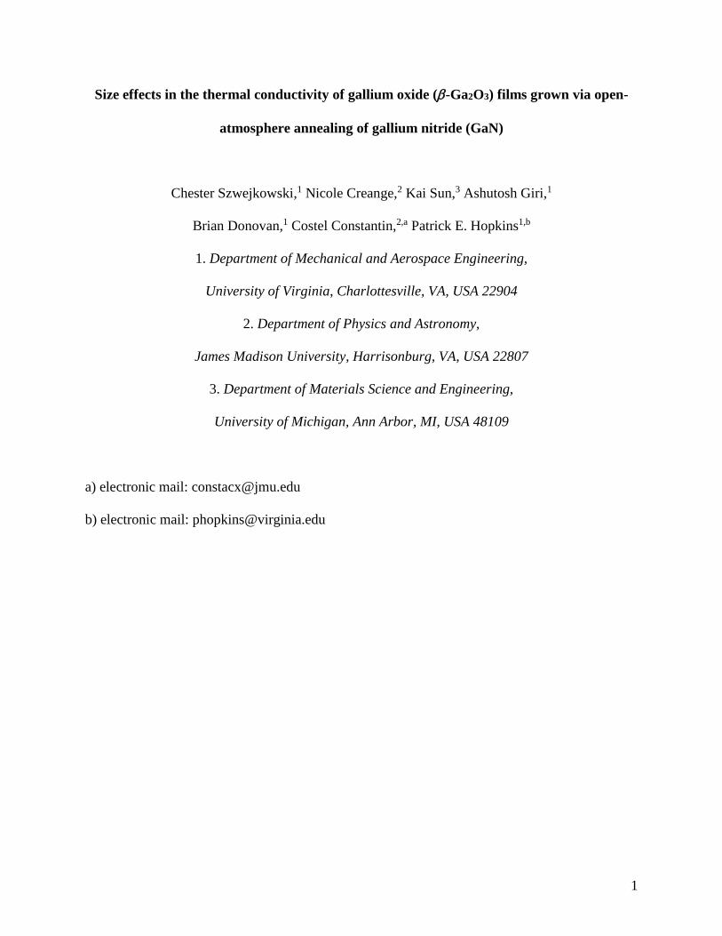
roughness of the gallium oxide was determined using a combination of atomic force microscopy
(AFM, Veeco DI Multimode IIIa) and mechanical profilometry. The unannealed samples (which
were the smoothest), had RMS roughness values (Rq) as low as 0.5 nm while the roughest sample
had Rq over 70 nm with many intermediate roughnesses in between (c.f., Fig. 1 a-h). The
roughness and compositional variance on the GaN surface where growth was initiated was
observed with transmission electron microscopy (TEM). The TEM images reveal that annealing
not only caused growth of a rough oxide layer but also changed the compositional abruptness of
the Ga2O3/GaN interface. Roughness and “spiking” at the interface can be seen in the TEM images
presented in Fig. 1 i-n. Table 1 summarizes the Ga2O3 thicknesses and surface roughnesses
determined from the AFM and TEM measurements.
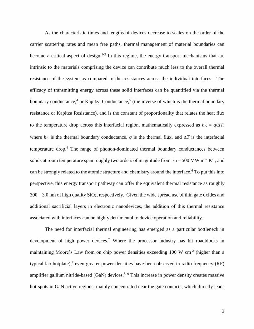
The chemistry of the oxide layer was determined using x-ray diffraction (XRD) and x-ray
photoelectron spectroscopy (XPS). In Fig. 2 a-d, we present the XRD spectra taken in the range of
2θ = 20° – 130° as a function of Rq obtained from a PANalytical X’Pert PRO MPD θ-2θ
diffractometer with x-ray radiation of Cu ( = 1.54060 Å for Cu Kα peak). The signature GaN
peaks are observed at 34.39(3)° (0002), 72.69(8)° (0004), and 125.89(1)° (0006). The Sapphire
peaks are observed at 41.63(1)° (0006), and 90.49(7)° (00012). The other peaks observed at 2θ =
31.16(6)°, 38.32(6)°, and 59.02(2)° correspond to crystallographic planes of (002), (202), and
(113) for β-Ga2O3. These β-Ga2O3 layers are polycrystalline and form crystallites that have single
crystal monoclinic structure, as determined via the AFM, TEM, and XRD. According to structure
factor calculations, the Miller Indices for such monoclinic structures should obey h+k = 2n with
n = 1, 2, 3, 4,..∞. The d-spacing for a monoclinic crystal structure is calculated according to
1
d2=
1
sin2(b )
h2
a2+k2 sin2(b )
b2+l2
c2-
2hl cos(b )
ac
é
ëê
ù
ûú , (1)
7
where hkl are the Miller Indices, abc are the unit cell lattice constants, and αβγ are the unit cell
internal angles. Equation 1 was useful to check the Miller indices for our β-Ga2O3 layers by using
well known values for a, b, and c as found in the literature.24 With Bragg’s law [i.e. n = 2d
sin()], we determined the d lattice spacings to be d002 = 2.867(4) Å, d202 = 2.346(6) Å, d113
=1.563(8) Å, in excellent agreement with those reported by Lv et al. (i.e. d002 = 2.82(9) Å, d202 =
2.34(4) Å, and d113 = 1.53(3) Å).25 The O1s XPS spectra in Fig. 2e are presented as a function of
surface roughness for our samples with Rq = 1.0, 4.9, 9.7, and 12.7 nm. The binding energies of
the examined elements were calibrated using C1s peak (284.6 eV) as a reference. The binding
energies for our samples were found to be 534.5 eV (Rq = 0.5 nm), 530.50 eV (Rq = 4.9 nm), 530.34
eV (Rq = 9.7 nm), and 530.15 eV (Rq = 12.7 nm). These O1s spectra indicate that the as-received
sample (i.e., not annealed and with 0.5 nm RMS roughness – blue curve in Fig. 2) contains a much
smaller signature of oxygen compared to the annealed samples; this is consistent with typical
thicknesses of native Ga2O3 on the GaN surface (i.e., a surface layer of 1-2 nm).26 It is important
to note that as the Ga2O3 layer increases in thickness, the O1s shifts towards smaller binding
energies, consistent with previous XPS studies showing the effect of the Ga2O3 on the GaN
spectrum.27
We measured the thicknesses of the gallium oxide layer with TEM, example micrographs
of which are presented in Fig. 1 i-n. The TEM analysis confirms that the increase in surface
roughness measured via AFM is directly correlated to an increase in oxide layer thickness. We
relate the thickness of gallium oxide to the roughness via a 3rd order polynomial fit (Fig. 3), and
use this calibration for analysis of our TDTR measurements, described in more detail below.
For TDTR measurements, we electron-beam evaporate thin metal films on the various
Ga2O3/GaN samples, using metals similar to those employed in electronic devices: 79 nm Au,

8
78nm Au with a 2 nm Ti wetting layer, and 89 nm Al. The film thicknesses were verified using a
combination of variable angle spectroscopic ellipsometry (VASE from J.A. Woollam) and
mechanical profilometry. In the case of the Al film, we were also able to confirm the film
thicknesses of picosecond acoustics.28, 29 An illustration of sample geometries studied in this work
is shown in Fig. 4. Table 1 summarizes the information for each set of samples.
III. THERMAL CONDUCTIVITY MEASUREMENTS OF THE -Ga2O3 FILMS
The thermal conductivities of the -Ga2O3 films were measured using time domain
thermoreflectance (TDTR);30 pertinent details of TDTR and corresponding data analyses can be
found in the literature.31-33 To briefly summarize, our TDTR experiment is a pump-probe technique
utilizing sub-picosecond laser pulses that are split into two paths: the pump and probe. The pump
energy is absorbed by the sample and causes a change in the surface temperature of the metal film.
This surface temperature decays based on the thermal properties of the materials underneath (in
our case, the -Ga2O3 film, the GaN film, the Al2O3 substrate, and the associated interfaces) and
the temporal change in temperature is subsequently monitored as a function of time via the change
in thermoreflectance of the probe pulse.34-36
In our specific experiments, we use the sub-picosecond pulses emitted from an 80 MHz
Ti:Sapphire laser system as a basis of our pump-probe experiments.. The pump path is modulated
at 8.8 MHz and focused onto the surface of the metal transducer layer while the thermoreflectivity
of the probe path is monitored at the pump frequency with a time-delay of up to 5.5 ns after the
initial heating event. The radii of the pump and probe paths are 25 µm and 6.5 µm, respectively,
so the heat flow is nearly entirely dominated by cross plane conduction (normal to the interfaces).
We used TDTR to characterize the thermal conductance through the -Ga2O3 films and associated

9
interfaces in the three sets of GaN samples (each set is referring to a different metal film
transducer). Each set had between six and eight samples with different surface roughnesses based
on the annealing conditions, as summarized in Table 1. Finally, at least three TDTR scans were
performed on each sample to ensure repeatability in our thermal measurements.
The method we use for our data analysis is described in detail in the literature.31-33 In short,
we fit a multilayer, diffusive thermal model that accounts for the periodic heating of the laser
pulses to our TDTR data. The inputs to our model analysis require knowledge of the heat capacity,
thermal conductivity, and thermal boundary conductance associated with each layer of the system.
We used literature values for the heat capacity of GaN (Ref. 37) and -Ga2O3 (Ref. 38) and for the
heat capacities and thermal conductivities of Al (Ref. 39) and Au (Ref. 40). At a modulation
frequency of 8.8 MHz, the thermal penetration depth in these samples is at most on the order of 2
µm. Thus, we are not sampling the sapphire layer or GaN/sapphire interface. For the as-received
samples, we determined the thermal conductivity of the GaN layer using a two layer model
(transducer/GaN), treating the nanometer of native oxide as an interface. This value for the thermal
conductivity of the GaN layer was used for the remaining annealed samples in that set. However,
because the GaN layer is so conductive, resistance to thermal transport is dominated by the GaN
interface and we are relatively insensitive to the thermal conductivity of the GaN.41 For the
annealed samples we used a three layer model (transducer/-Ga2O3/GaN), fitting the thermal
conductivity of the -Ga2O3 layer and the thermal boundary conductance at the transducer/-
Ga2O3 interface. In this analysis, we assumed that the thermal boundary conductance at the -
Ga2O3/GaN interface was very large (i.e., we assumed that this interface offers negligible
resistance), so that the measured thermal conductivities of the -Ga2O3 layer from the TDTR
measurements are in fact “effective” thermal conductivities that are also influenced by the
10
resistance at the -Ga2O3/GaN interface. As discussed later, we through data analysis of the
effective thermal conductivities as a function of film thickness, we resolve the intrinsic thermal
conductivity of the -Ga2O3 and the thermal boundary conductance across the transducer/-Ga2O3
interface adapting a method used by Lee et al.42 The uncertainty in our measurements factored in
the repeatability of the measurements, uncertainty in film thicknesses, uncertainty in the thermal
conductivity of the metal film, and uncertainty in the heat capacity of GaN and Ga2O3. From this,
the mean uncertainty in our TDTR measurements was ~10%.
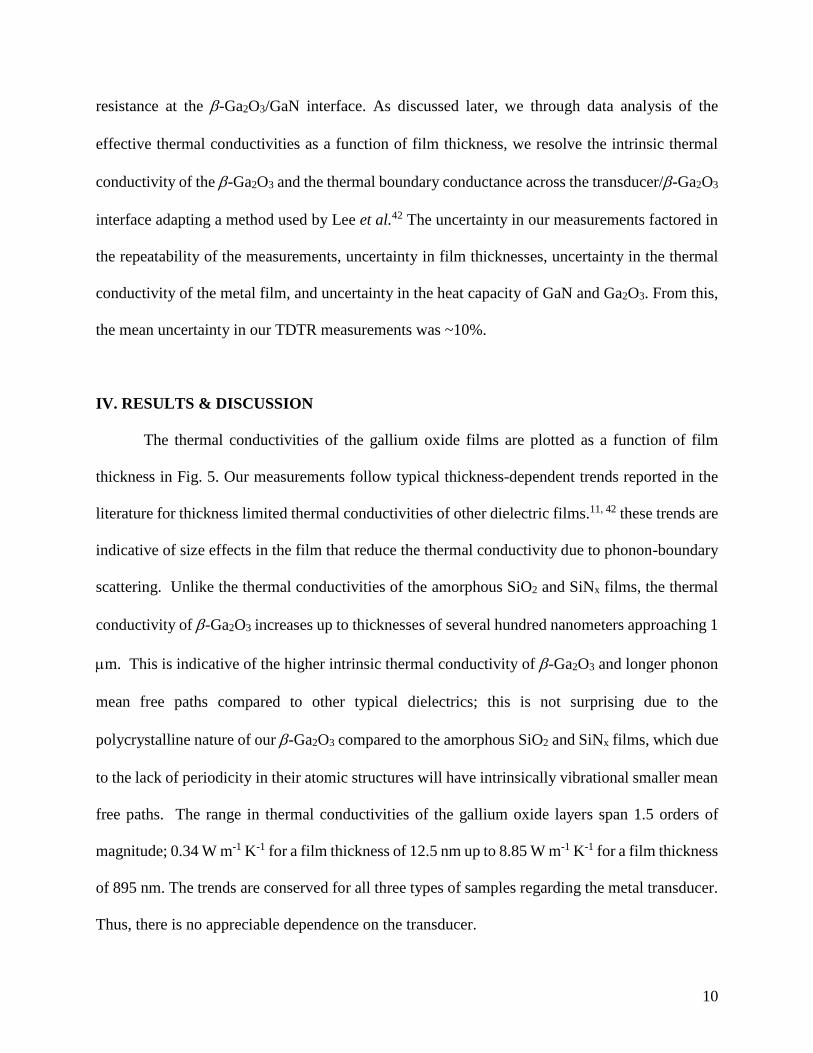
IV. RESULTS & DISCUSSION
The thermal conductivities of the gallium oxide films are plotted as a function of film
thickness in Fig. 5. Our measurements follow typical thickness-dependent trends reported in the
literature for thickness limited thermal conductivities of other dielectric films.11, 42 these trends are
indicative of size effects in the film that reduce the thermal conductivity due to phonon-boundary
scattering. Unlike the thermal conductivities of the amorphous SiO2 and SiNx films, the thermal
conductivity of -Ga2O3 increases up to thicknesses of several hundred nanometers approaching 1
m. This is indicative of the higher intrinsic thermal conductivity of -Ga2O3 and longer phonon
mean free paths compared to other typical dielectrics; this is not surprising due to the
polycrystalline nature of our -Ga2O3 compared to the amorphous SiO2 and SiNx films, which due
to the lack of periodicity in their atomic structures will have intrinsically vibrational smaller mean
free paths. The range in thermal conductivities of the gallium oxide layers span 1.5 orders of
magnitude; 0.34 W m-1 K-1 for a film thickness of 12.5 nm up to 8.85 W m-1 K-1 for a film thickness
of 895 nm. The trends are conserved for all three types of samples regarding the metal transducer.
Thus, there is no appreciable dependence on the transducer.
11
From the data in Fig. 5, we can determine the intrinsic thermal conductivity of bulk -
Ga2O3 while relating the reduction in thermal conductivity due to phonon-boundary scattering to
the thermal boundary conductance across the -Ga2O3/GaN interface. Using the expression
presented by Lee et al.,42 the intrinsic thermal conductivity of -Ga2O3 can be derived from our
data via
km =k i
1+k ihKd
, (2)
where m is the measured thermal conductivity, κi is the intrinsic thermal conductivity of the -
Ga2O3, hK is the thermal boundary conductance, and d is the thickness of the -Ga2O3. Equation
2 treats the metal/-Ga2O3 thermal conductance, the thermal conductivity of the -Ga2O3 film, and
the -Ga2O3/GaN thermal conductance as resistors in series. However, we rule out the inclusion
of the resistance across the metal/-Ga2O3 in calculations of Eq. 2 due to the following two
reasons: i) in our TDTR analysis of the thermal conductivity of the -Ga2O3, we fit both the
metal/-Ga2O3 thermal boundary conductance and the -Ga2O3 thermal conductivity, thereby
independently determining the thermal conductivity of the -Ga2O3 from the metal/-Ga2O3
thermal boundary conductance. During this analysis, we determine that we are inherently
insensitive to the metal/-Ga2O3 boundary conductance due to the relatively larger resistance of
the -Ga2O3 film; and ii) as shown in the inset of Fig. 5, we do not show any systematic, noticeable
dependence in the measured thermal conductivity of the -Ga2O3 for the samples with different
metallic transducers. Since we have previously shown that the thermal boundary conductance
across these metal films/native -Ga2O3/GaN interfaces can vary by a factor of five depending on
the metal film,41 we conclude that this metal/-Ga2O3 is not contributing to the thermal processes

12
measured in our TDTR experiments. Therefore, the value for thermal boundary conductance in
Eq. 2 is representative of the thermal transport across the -Ga2O3/GaN interface.
The inset graph shows our data and the model, adapted from Lee et al.,42 represented by a
black dotted line. The thermal boundary conductance is calculated to be 31.2 ± 8.1 MW m-2 K-1
and the corresponding intrinsic thermal conductivity of bulk -Ga2O3 is 9.7 ± 2.5 W m-1 K-1. This
thermal conductivity is slightly lower than a previous measurement of the thermal conductivity of
bulk, single crystalline -Ga2O3 (13 W m-1 K-1 – black dotted line in Fig. 5).43 Given the
polycrystalline nature of our -Ga2O3 films, this reduction in thermal conductivity is not
surprising. Although the intrinsic thermal conductivity of our -Ga2O3 is nearly an order of
magnitude larger than the other typical gate insulators shown in Fig. 5 (SiO2 and SiNx), boundary
scattering effects are pronounced enough that for typical gate oxide thicknesses, the effective
thermal conductivity is reduced to similar values as these gate dielectric materials.
The opportunity for thermal benefits in GaN devices arises in manipulating the thermal
boundary conductance across the -Ga2O3/GaN interface. As previously mentioned, we
determined hK across this interface as 31.2 ± 8.1 MW m-2 K-1. This is on the same order as the
room temperature thermal boundary conductances reported for SiO2/Si interfaces (hK = 50 MW m-
2 K-1)42 and dislocation dense GaSb/GaAs interfaces grown epitaxially (hK = 10 – 20 MW m-2 K-
1).44 Our TEM analyses shown in Fig. 1 indicate the “imperfect” nature of the boundary between
the -Ga2O3 and GaN, which can lead to large reductions in thermal boundary conductance.6 Given
this relatively low conductance (large resistance) associated with this interface compared to the
intrinsic thermal conduction mechanisms in bulk -Ga2O3, the opportunity exists to engineer this
interface and thereby increase the overall thermal conduction across a metal/-Ga2O3/GaN
junction.
13
The possibility of increasing the thermal conductance across metal/-Ga2O3/GaN junctions
has tremendous implications for thermal mitigation of GaN-based devices by engineering hot spots
around gate regions. Beta-phase Ga2O3 has many of the necessary electronic characteristics to be
used as a gate oxide: low density of states at the -Ga2O3/GaN interface,45 high breakdown field,45
high dielectric constant,45 and wide band gap.46 Although, the-Ga2O3/GaN valence and
conduction band offsets are low; 1.4 eV and 0.1 eV respectively,47 compared to 4.4 eV and 3.4 eV
for SiO2/Si48 which could lead to increased leakage current. Furthermore,-Ga2O3 is very
chemically stable, even in concentrated acids,49 which could be problematic or promotional for
chemical etching procedures depending on what the end goal is. Thus, further chemical and
electronic research is necessary to realize the full potential of-Ga2O3 as a gate dielectric.
However, this issue is outside the scope of this study; our focus is thermal characterization. Our
thermal measurements of open atmosphere-grown -Ga2O3 demonstrate the intrinsically larger
thermal conductivity and mean free path compared to typical gate dielectrics, indicating the
possibility for increase thermal spreading of heat from localized hot spots at gate/channel contacts
compared to typical dielectric and passivation layers. This makes annealing of GaN to form
surface layers of -Ga2O3 a promising candidate for gate dielectrics and other surface passivation
layers in next generation GaN devices.
V. SUMMARY
Our work reports on the size effects of the thermal conductivity of beta-phase gallium oxide
(β-Ga2O3) thin films, a component of typical gate oxides used in such devices. We use time domain
thermoreflectance to measure the thermal conductivity of a variety of polycrystalline β-Ga2O3
films of different thicknesses grown via open atmosphere annealing of GaN surface. We confirm
14
that the β-Ga2O3 grown from annealing the the GaN surface is phase-pure, and varies in both
surface roughness and diffusion into the GaN based on annealing time. The effective thermal
conductivity of β-Ga2O3 can span 1.5 orders of magnitude, increasing with an increased film
thickness, which is indicative of the relatively large intrinsic thermal conductivity of bulk β-Ga2O3
(9.7 ± 2.5 W m-1 K-1) and large mean free paths compared to typical gate dielectrics commonly
used in GaN device contacts. By conducting TDTR measurement with different metal transducers
(Al, Au, and Au with a Ti wetting layer), we attribute this variation in effective thermal
conductivity to size effects in the β-Ga2O3 film resulting from phonon scattering at the β-
Ga2O3/GaN interface. From our measurements, we quantify the thermal boundary conductance
across the β-Ga2O3/GaN interface as 31.2 ± 8.1 MW m-2 K-1, in the range of typical thermal
boundary conductances previously observed non-metal/non-metal interfaces. The measured
thermal properties of open atmosphere-grown β-Ga2O3 and its interface with GaN set the stage for
thermal engineering of gate contacts in high frequency GaN-based devices.
ACKNOWLEDGMENTS
The material is based upon work partially supported by the Air Force Office of Scientific Research
under AFOSR Award No. FA9550-14-1-0067 (Subaward No. 5010-UV-AFOSR-0067), the
National Science Foundation (CBET-1339436) and the Commonwealth Research
Commercialization Fund (CRCF) of Virginia.

15
REFERENCES
1. D. G. Cahill, P. V. Braun, G. Chen, D. R. Clarke, S. Fan, K. E. Goodson, P. Keblinski, W. P. King, G. D. Mahan, A. Majumdar, H. J. Maris, S. R. Phillpot, E. Pop and L. Shi, "Nanoscale thermal transport. II. 2003-2012," Applied Physics Reviews 1, 011305 (2014).
2. D. G. Cahill, W. K. Ford, K. E. Goodson, G. D. Mahan, A. Majumdar, H. J. Maris, R. Merlin and S. R. Phillpot, "Nanoscale thermal transport," Journal of Applied Physics 93, 793-818 (2003).
3. G. Chen, Nanoscale Energy Transport and Conversion: A Parallel Treatment of Electrons, Molecules, Phonons, and Photons (Oxford University Press, New York, 2005).
4. E. T. Swartz and R. O. Pohl, "Thermal boundary resistance," Reviews of Modern Physics 61, 605-668 (1989).
5. P. L. Kapitza, "The study of heat transfer in Helium II," Zhurnal eksperimentalnoi i teoreticheskoi fiziki 11, 1-31 (1941).
6. P. E. Hopkins, "Thermal transport across solid interfaces with nanoscale imperfections: Effects of roughness, disorder, dislocations, and bonding on thermal boundary conductance," ISRN Mechanical Engineering 2013, 682586 (2013).
7. E. Pop, "Energy dissipation and transport in nanoscale devices," Nano Research 3, 147-169 (2010).
8. A. N. Smith and J. P. Calame, "Impact of thin film thermophysical properties on thermal management of wide bandgap solid-state transistors," International Journal of Thermophysics 25, 409-422 (2004).
9. R. J. Trew, "SiC and GaN transistors - Is there one winner for microwave power applications?," Proceedings of the IEEE 90, 1032-1047 (2002).
10. S.-M. Lee, D. G. Cahill and T. H. Allen, "Thermal conductivity of sputtered oxide films," Physical Review B 52, 253-257 (1995).
11. R. M. Costescu, A. J. Bullen, G. Matamis, K. E. O'Hara and D. G. Cahill, "Thermal conductivity and sound velocities of hydrogen-silsequioxane low-k dielectrics," Physical Review B 65, 094205 (2002).
12. C. S. Gorham, J. T. Gaskins, G. N. Parsons, M. D. Losego and P. E. Hopkins, "Density dependence of the room temperature thermal conductivity of atomic layer deposition grown amorsphous alumina (Al2O3)," Applied Physics Letters 104, 253107 (2014).
13. J. W. Johnson, B. Luo, F. Ren, B. P. Gila, W. Krishnamoorthy, C. R. Abernathy, S. J. Pearton, J. I. Chyi, T. E. Nee, C. M. Lee and C. C. Chuo, "Gd2O3/GaN metal-oxide-semiconductor field-effect transistor," Applied Physics Letters 77, 3230 (2000).
14. T. D. Lin, H. C. Chiu, P. Chang, L. T. Tung, C. P. Chen, M. Hong, J. Kwo, W. Tsai and Y. C. Wang, "High-performance self-aligned inversion-channel In0.53Ga0.47As metal-oxide-semiconductor field-effect-transistor with Al2O3/Ga2O3(Gd2O3) as gate dielectrics," (2008).
15. F. Ren, M. Hong, S. N. G. Chu, M. A. Marcus, M. J. Schurman, A. Baca, S. J. Pearton and C. R. Abernathy, "Effect of temperature on Ga2O3(Gd2O3)/GaN metal-oxide-semiconductor field-effect transistors," Applied Physics Letters 73, 3893 (1998).
16. V. R. Reddy, M. Ravinandan, P. K. Rao and C.-J. Choi, "Effects of thermal annealing on the electrical and structural properties of Pt/Mo Schottky contacts on n-type GaN," Journal of Materials Science: Materials in Electronics 20, 1018 (2009).

16
17. W. Cao and S. K. Dey, "Microstructure and properties of sol-gel derived Pb(Zr0.3Ti0.7)O3 thin films on GaN/sapphire for nanoelectromechanical systems," Journal of Sol-Gel Science & Technology 40, 389 (2007).
18. A. Y. Polyakov, N. B. Smirnov, A. V. Govorkov, A. A. Shlensky and S. J. Pearton, "Influence of high-temperature annealing on the properties of Fe doped semi-insulating GaN structure," Journal of Applied Physics 95, 5591 (2004).
19. Y. Hayashi, R. Hasunuma and K. Yamabe, "Generation and Growth of Atomic-scale Roughness at Surface and Interface of Silicon Dioxide Thermally Grown on Atomically Flat Si Surface," Key Engineering Materials 470, 110 (2011).
20. H. Döscher, G. Lilienkamp, P. Iskra, M. Kazempoor and W. Daum, "Thermal stability of thin ZrO2 films prepared by a sol-gel process on Si(001) substrates," Journal of Vaccum Science & Technology B 28, C5B5 (2010).
21. Y. Dong, R. M. Feenstra and J. E. Northrup, "Oxidized GaN(0001) surfaces studied by scanning tunneling microscopy and spectroscopy and by first-principles theory," Journal of Vaccum Science & Technology B 24, 2080 (2006).
22. C. J. Lu, A. V. Davydov, D. Josell and L. A. Bendersky, "Interfacial reactions of Ti/n-GaN contacts at elevated temperature," Journal of Applied Physics 925, 245 (2003).
23. B. P. Luther, S. E. Mohney, T. N. Jackson, M. A. Khan, Q. Chen and J. W. Yang, "Investigation of the mechanism for Ohmic contact formation in Al and Ti/Al contacts to n-type GaN," Applied Physics Letters 70, 57 (1997).
24. S. S. Kumar, E. J. Rubio, M. Noor-A-Alam, G. Martinez, S. Manandhar, V. Shutthanandan, S. Thevuthasan and C. V. Ramana, ""Structure, Morphology, and Optical Properties of Amourphous and Nanocrystalline Gallium Oxide Thin Films," Journal of Physical Chemistry 117, 4194 (2013).
25. Y. Lv, L. Yu, G. Zha, D. Zheng and C. Jiang, "Application of soluble salt-assisted route to
synthesis of -Ga2O3 nanopowders," Applied Physics A: Materials Science & Processing 114, 351 (2014).
26. X. A. Cao, S. J. Pearton, G. Dang, A. P. Zhang, F. Ren and J. M. Van Hove, "Effects of interfacial oxides on Schottky barrier contacts to n- and p-type GaN," Applied Physics Letters 75, 4130 (1999).
27. K. Prabhakaran, T. G. Andersson and K. Nozawa, "Nature of native oxide on GaN surface and its reaction with Al," Applied Physics Letters 69, 3212 (1996).
28. G. T. Hohensee, W.-P. Hsieh, M. D. Losego and D. G. Cahill, "Interpreting picosecond acoustics in the case of low interface stiffness," Review of Scientific Instruments 83, 114902 (2012).
29. C. Thomsen, J. Strait, Z. Vardeny, H. J. Maris, J. Tauc and J. J. Hauser, "Coherent Phonon Generation and Detection by Picosecond Light Pulses," Physical Review Letters 53, 989-992 (1984).
30. D. G. Cahill, K. Goodson and A. Majumdar, "Thermometry and Thermal Transport in Micro/Nanoscale Solid-State Devices and Structures," Journal of Heat Transfer 124, 223 (2002).
31. P. E. Hopkins, J. R. Serrano, L. M. Phinney, S. P. Kearney, T. W. Grasser and C. T. Harris, "Criteria for cross-plane dominated thermal transport in multilayer thin film systems during modulated laser heating," Journal of Heat Transfer 132, 081302 (2010).

17
32. A. J. Schmidt, X. Chen and G. Chen, "Pulse accumulation, radial heat conduction, and anisotropic thermal conductivity in pump-probe transient thermoreflectance," Review of Scientific Instruments 79, 114902 (2008).
33. D. G. Cahill, "Analysis of heat flow in layered structures for time-domain thermoreflectance," Review of Scientific Instruments 75, 5119 (2004).
34. R. Rosei, "Temperature modulation of the optical transitions involving the Fermi surface in Ag: Theory," Physical Review B 10, 474 (1974).
35. R. Rosei, C. H. Culp and J. H. Weaver, "Temperature modulation of the optical transitions involving the Fermi surface in Ag: Experimental," Physical Review B 10, 484 (1974).
36. R. Rosei and D. W. Lynch, "Thermomodulation spectra of Al, Au, and Cu," Physical Review B 5, 3883 (1972).
37. R. Kremer, M. Cardona, E. Schmitt, J. Blumm, S. Estreicher, M. Sanati, M. Bockowski, I. Grzegory, T. Suski and A. Jezowski, "Heat capacity of α-Ga N: Isotope effects," Physical Review B 72, 075209 (2005).
38. G. B. Adams Jr. and H. L. Johnston, "Low Temperature Heat Capacities of Inorganic Solids. XI. The Heat Capacity of b-Gallium Oxide from 15 to 300oK," Journal of the American Chemical Society 74, 4788 (1952).
39. G. T. Furukawa, M. L. Reilly and J. S. Gallagher, "Critical Analysis of Heat—Capacity Data and Evaluation of Thermodynamic Properties of Ruthenium, Rhodium, Palladium, Iridium, and Platinum from 0 to 300K. A Survey of the Literature Data on Osmium," Journal of Physical and Chemical Reference Data 3, 163-209 (1974).
40. G. T. Furukawa, W. G. Saba and M. L. Reilly, Critical analysis of the heat-capacity data of the literature and evaluation of thermodynamic properties of copper, silver, and gold from 0 to 300 K, DTIC Document, 1968.
41. B. F. Donovan, C. J. Szwejkowski, J. C. Duda, R. Cheaito, J. T. Gaskins, C.-Y. P. Yang, D. L. Medlin, C. Constantin, R. E. Jones and P. E. Hopkins, Thermal boundary conductance across metal-Gallium Nitride (GaN) interfaces from 80 - 450 K, University of Virginia, 2014.
42. S.-M. Lee and D. G. Cahill, "Heat Transport in thin dielectric films," Journal of Applied Physics 81, 2590 (1997).
43. E. G. Villora, K. Shimamura, T. Ujiie and K. Aoki, "Electrical conductivity and lattice expansion of β-Ga 2 O 3 below room temperature," Applied Physics Letters 92, 202118-202118-202113 (2008).
44. P. E. Hopkins, J. C. Duda, S. P. Clark, C. P. Hains, T. J. Rotter, L. M. Phinney and G. Balakrishnan, "Effect of dislocation density on thermal boundary conductance across GaSb/GaAs interfaces," Applied Physics Letters 98, 161913 (2011).
45. C.-T. Lee, H.-W. Chen and H.-Y. Lee, "Metal–oxide–semiconductor devices using Ga 2 O 3 dielectrics on n-type GaN," Applied Physics Letters 82, 4304-4306 (2003).
46. M. D. Losego, Interfacing Epitaxial Oxides to Gallium Nitride, North Carolina State University, 249, 2008.
47. W. Wei, Z. Qin, S. Fan, Z. Li, K. Shi, Q. Zhu and G. Zhang, "Valence band offset of b-Ga2O3/wurtzite GaN heterostructure measured by X-ray photoelectron spectroscopy," Nanoscale Research Letters 7, 562 (2012).
18
48. A. Alkauskas, P. Broqvist, F. Devynck and A. Pasquarello, "Band Offsets at Semiconductor-Oxide Interfaces from Hybrid Density-Functional Calculations," Physical Review Letters 101, 106802 (2008).
49. M. Passlack, E. F. Schubert, W. S. Hopson, M. Hong, N. Moriya, S. N. G. Chu, K. Konstadinidis, J. P. Mannaerts, M. L. Schnoes and G. J. Zydzik, "Ga2O3 films for electronic and optoelectronic applications," Journal of Applied Physics 77, 686 (1995).
19
Table 1. Three sets of samples were fabricated regarding the metal transducer that was deposited. The roughness of
the RMS surface of the samples before transducer deposition (Rq) and the thickness of the gallium oxide layer (d) are
summarized.
Transducer Au (79 nm) Al (89 nm) Au (78 nm) / Ti (2 nm)
β-Ga2O3 Rq (nm) d (nm) Rq (nm) d (nm) Rq (nm) d (nm)
0.9 1.5 0.8 1.3 0.8 1.3
6.6 18.1 4.0 9.4 6.9 19.2
11.6 40.3 5.0 12.5 13.5 50.7
25.9 141.9 10.8 36.3 33.8 220.4
45.9 369.6 14.5 56.5 43.2 333.4
60.2 585.8 19.4 89.0 77.2 895.1
30.2 182.7
41.6 312.7
65.6 679.0

20
Figure 1. (a) – (h) Atomic force microscopy images of Ga2O3-GaN-Sapphire surfaces for Rq = 0.81 – 70.60 nm. (i) –
(n) Cross-section high resolution transmission electron microscopy for sample with Rq = 0.88 – 77.22 nm.
21
Figure 2. XRD-XPS. (a) X-ray diffraction (θ-2θ) of β-Ga2O3-GaN-Sapphire (0001) thin films as a function of surface
roughness root mean square (Rq) for Rq = 0.9 – 104.0 nm. (b)-(d) Scaled up figures for the β-Ga2O3 signature peaks
(i.e. 2θ = 31.6°, 38.3°, 59.0°). (e) X-ray photoemission spectroscopy for oxygen O1s peak observed at ~ 530 eV.

22
Figure 3. β-Ga2O3 thickness measured via TEM vs. surface roughness measured via AFM. The relationship is modeled
by the red dotted line with a third order polynomial equation: 𝑑 = −0.0004(𝑅𝑞)3+ 0.1667(𝑅𝑞)
2+ 0.6869(𝑅𝑞) +
1.5. This was found to be a statistically sound correlation (R2 = 0.975, t = 12.6, tα=0.005 = 4.60).

23
Figure 4. Illustration of sample geometries studied in this work. The fabrication of our samples includes two stages:
the gallium oxide growth and then the metal film deposition. Starting with the commercially available GaN on
sapphire, the oxide was grown via open atmosphere annealing for ten minute cycles at temperatures between 900 –
1050°C; longer anneals increased the roughness at the oxide surface (indicated by the textured line above the oxide
layer). Various metal films were then electron-beam evaporated on top including aluminum, gold, and gold with a
titanium adhesion layer.

24
Figure 5. Measured Thermal conductivity as a function of film thickness for our -Ga2O3 films compared to other
thin film dielectrics. The thermal conductivity of gallium oxide (filled squares) increases with increased film thickness
and approaches the previously report bulk thermal conductivity (dotted line).43 This follows the same trend as other
dielectric films reported by Lee et al.42 (open cirles: SiO2; diamonds: SiNx) and Costescu et al.11 (open triangles: SiO2)
and is attributed to boundary scattering. (inset) Measured thermal conductivity vs. thickness of -Ga2O3 films with
the different metal transducers used (filled circles: aluminum; filled diamonds: gold with titanium wetting layer; filled
squares: gold), suggesting that the thermal resistance at the transducer/-Ga2O3 is negligible; from this, we conclude
that the primary mechanism driving the size effects in the measured thermal conductivities of these films is the thermal
resistance associated with the -Ga2O3/GaN interface The black dashed line is the model used to resolve the thermal
boundary conductance across the -Ga2O3/GaN interface, adapted from Lee et al.42
Recommended