Shi-Yu Huang and Ya-Chun Lai
Design Technology Center (DTC)National Tsing-Hua University, HsinChu, Taiwan
Die-Hard SRAM DesignUsing Per-Column Timing Tracking
Feb. 10, 2007 @ Las Vegas (IC-DFN)

2/25
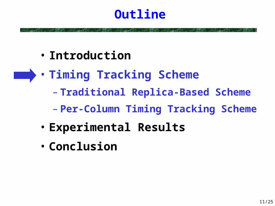
Outline
• Introduction
• Timing Tracking Scheme
– Traditional Replica-Based Scheme
– Our Scheme
• Experimental Results
• Conclusion
3/25
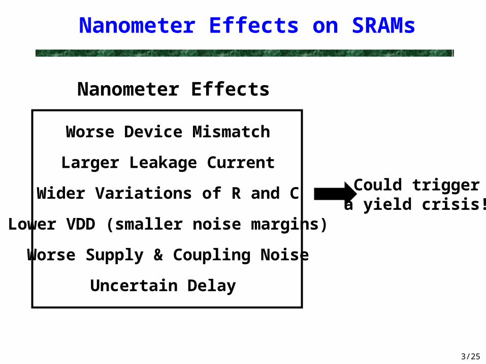
Nanometer Effects on SRAMs
Larger Leakage Current
Worse Device Mismatch
Worse Supply & Coupling Noise
Lower VDD (smaller noise margins)
Uncertain Delay
Nanometer Effects
Wider Variations of R and C Could triggera yield crisis!

4/25
SRAM Memory Architecture
RowDecoder
...
A9
A8
A0
Sense Amplifier / Drivers
Column DecoderA19
A10
Input-Output(M bits)
bit line
word line
CSWEOE

5/25
Reading An SRAM Cell
10 Q
Q’
cellcurrent
Wordline
An SRAM Cell
BL BL
pulsed wordline
BL
BLBitlines’ Waveforms
6/25
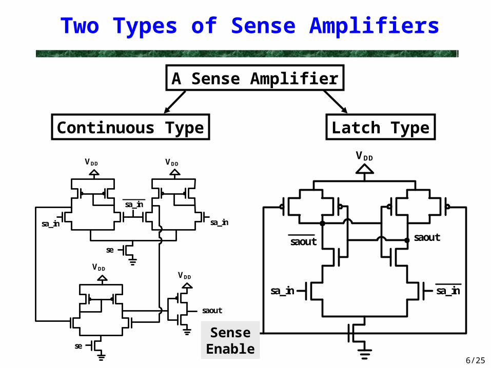
Two Types of Sense Amplifiers
Continuous Type Latch Type
sa_in
se
saout
VDD
sa_in
saout
sa_in
se
saout
VDD VDD
sa_in
VDDVDD
se
sa_in
SenseEnable
A Sense Amplifier

7/25
Three Major Problems for SRAM
• Mismatch in Bit Cells and Sense Amplifiers
– Vt mismatch shrinks the noise margin
• Bitline Leakage Current
– Could cause failure for READ operations
• Timing Tracking
– When to turn on sense amplifiers?
– When to turn off wordline? (pulsed wordline)

8/25
X-Calibration for Leakage Tolerance
(Presented in Last IC-DFN)
Leakage is calibrated in two steps:
Transform the effectsof the bitline leakage
to a Voffset between (BL, BL)
Deduct Voffset
from the input of the sense amplifierWhen performing sense amplification
cellcellcellcellcellcellcellcell
S.A.
BL01111111
10000000
LeakageCurrent
BL
X-calibration circuit
1.8V 1.5V
9/25
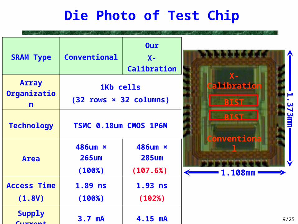
Die Photo of Test Chip
1.108mm
1.373mm
BIST
Conventional
BIST
X-Calibration
SRAM Type ConventionalOur
X-Calibration
Array
Organization
1Kb cells
(32 rows × 32 columns)
Technology TSMC 0.18um CMOS 1P6M
Area486um × 265um
(100%)
486um × 285um
(107.6%)
Access Time
(1.8V)
1.89 ns
(100%)
1.93 ns
(102%)
Supply Current
(mA)
3.7 mA
(100%)
4.15 mA
(112%)
10/25
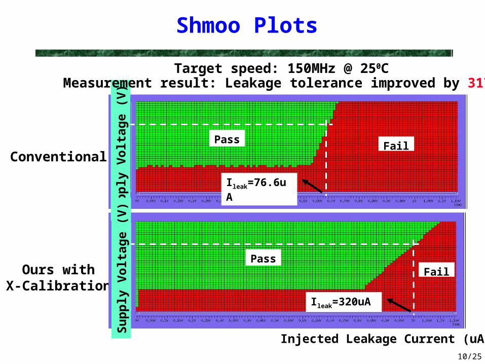
Shmoo Plots
Conventional
Ours withX-Calibration
PassFail
Ileak=76.6uA
PassFail
Ileak=320uA
Injected Leakage Current (uA)
Supp
ly V
olta
ge (
V)
Supp
ly V
olta
ge (
V)
Target speed: 150MHz @ 250CMeasurement result: Leakage tolerance improved by 317%
11/25
Outline
• Introduction
• Timing Tracking Scheme
– Traditional Replica-Based Scheme
– Per-Column Timing Tracking Scheme
• Experimental Results
• Conclusion
12/25
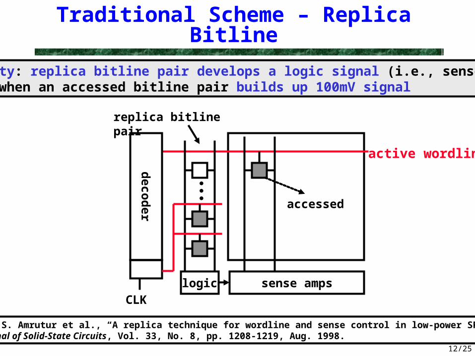
Traditional Scheme – Replica Bitline
sense amps
CLK
logic
deco
der
replica bitline pair
Ref: B. S. Amrutur et al., “A replica technique for wordline and sense control in low-power SRAMs,” IEEE Journal of Solid-State Circuits, Vol. 33, No. 8, pp. 1208-1219, Aug. 1998.
Property: replica bitline pair develops a logic signal (i.e., sense enable)when an accessed bitline pair builds up 100mV signal
active wordline
accessed
13/25
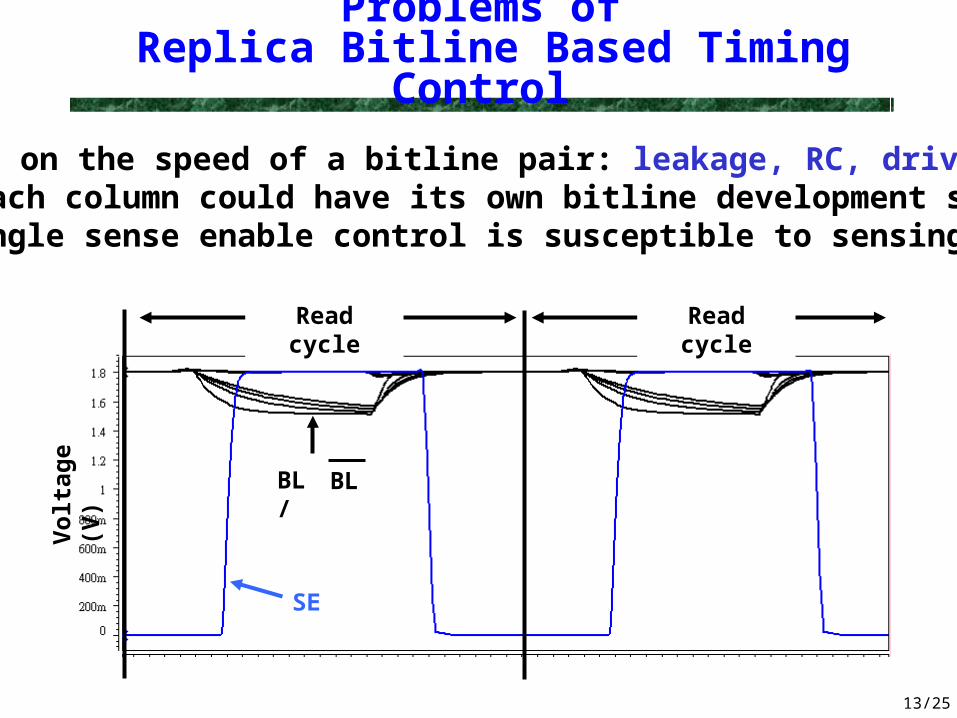
Problems of Replica Bitline Based Timing Control
Vo
ltag
e (V
)
Read cycle Read cycle
BL / BL
SE
The factors on the speed of a bitline pair: leakage, RC, driving of cell Each column could have its own bitline development speed A single sense enable control is susceptible to sensing errors

14/25
Adaptive Sensing ControlV
olt
age
(V)
Read cycle Read cycle
BL / BL
SE
Each sense amp. adapts to its current driving bitline pair!
15/25
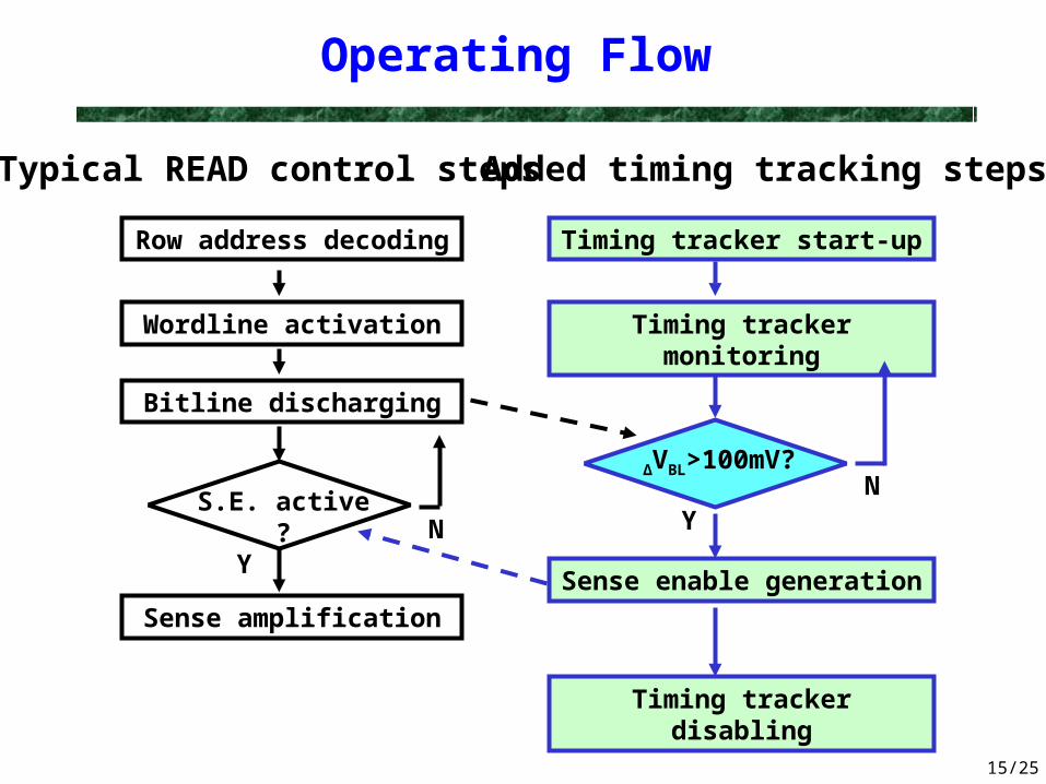
Operating Flow
Row address decoding
Wordline activation
Bitline discharging
Sense amplification
Timing tracker start-up
Sense enable generation
Timing tracker disabling
Timing tracker monitoring
ΔVBL>100mV?N
YS.E. active ?
NY
Typical READ control steps Added timing tracking steps
16/25
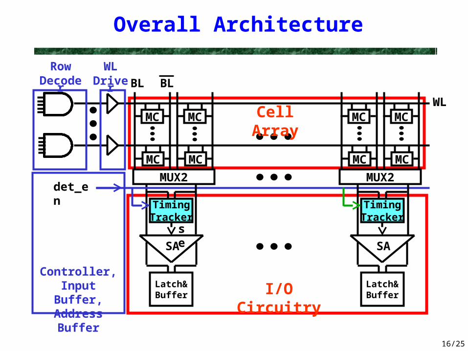
Overall Architecture
TimingTracker
Latch&Buffer
SA
TimingTracker
Latch&Buffer
SA
det_en
se
BL BL
WL
WLDriver
RowDecoder
Cell Array
MUX2
MC
MC
MC
MC
MUX2
MC
MC
MC
MC
I/O CircuitryController,
Input Buffer, Address Buffer

17/25
Transient Waveforms for Read
CLK
BL / BL
WL
se
det_en
TimingTracker
Latch&Buffer
SA
se
BL BL
MUX2
MC
MC
MC
MC
det_en
WLDriver
RowDecoder
Desired property: SE goes high when bitline pair has 100mV!
18/25
Outline
• Introduction
• Timing Tracking Scheme
– Traditional replica-based scheme
– Per-Column Timing Tracking
• Experimental Results
• Conclusion

19/25
0.4
0.6
0.8
1
1.2
0 10 20 30 40 50 60
Effect of Variation on Sense Amp. Vt
• As Vt mismatch in sense amplifier becomes excessive,
the probability of read failure increases.
Pas
s R
ate
Local standard deviation of Vt for transistors in SA (mV)
dummy bitline
proposalproposed
replica-based
20/25
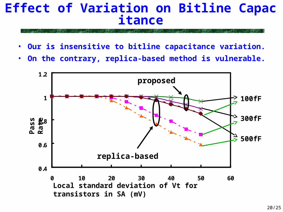
Effect of Variation on Bitline Capacitance
• Our is insensitive to bitline capacitance variation.
• On the contrary, replica-based method is vulnerable.
0.4
0.6
0.8
1
1.2
0 10 20 30 40 50 60
Pas
s R
ate
Local standard deviation of Vt for transistors in SA (mV)
Proposal
dummy bitline
500fF
300fF
100fF
proposed
replica-based

21/25
Layout of Test Chip
1.108mm1.108mm
1.208mm
1.208mm
ComparedCompared
ProposedProposed
CapacitoCapacitorr
(Technology): TSMC 0.18um CMOS 1P6M
(Creating Nanometer Effects): We used different loadings ondifferent bitlines so as to mimicthe different operating speedsin deeper nanometer technologies
22/25
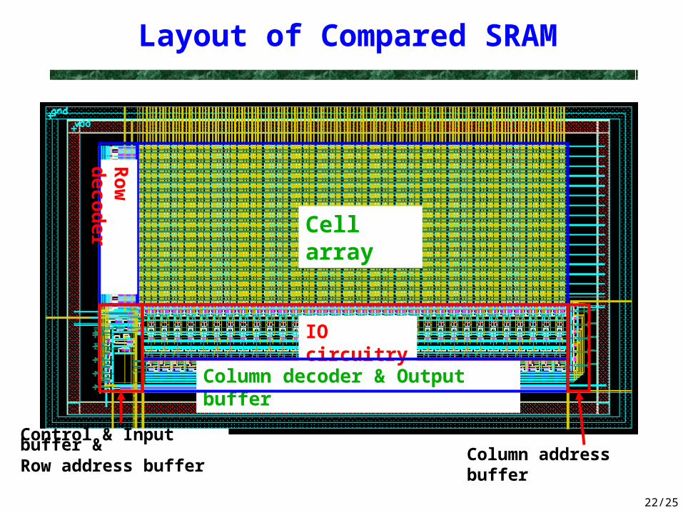
Layout of Compared SRAM
Cell array
Column decoder & Output buffer
IO circuitry
Ro
w d
eco
de
r
Control & Input buffer &Row address buffer Column address buffer

23/25
Layout of Proposed SRAM
Cell array
Column decoder & Output buffer
IO circuitry & Timing tracker
Ro
w d
eco
de
r
Control & Input buffer &Row address buffer Column address buffer

24/25
Test Chip Characteristics
Technology TSMC 0.18um CMOS 1P6M
Package 40-pin S/B
SRAM macro organization 32 rows x 64 columns
Test chip area 1.108 mm x 1.208 mm
Power supply voltage 1.8 V
Operating Clock frequency 200 MHz
Power dissipation for compared SRAM 13.185 mW (100%)
Power dissipation for proposed SRAM 17.930 mW (136.8%)
Access time for compared SRAM 1.969 ns
Access time for proposed SRAM 2.301 ns (116.8%)
25/25
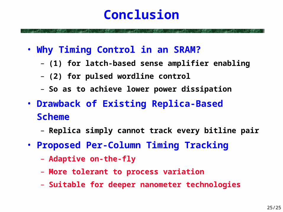
Conclusion
• Why Timing Control in an SRAM?– (1) for latch-based sense amplifier enabling
– (2) for pulsed wordline control
– So as to achieve lower power dissipation
• Drawback of Existing Replica-Based Scheme– Replica simply cannot track every bitline pair
• Proposed Per-Column Timing Tracking– Adaptive on-the-fly
– More tolerant to process variation
– Suitable for deeper nanometer technologies
Recommended


![C201700217a02 ODII ] M Route A10 …FileLinkedWithBanner...After Tsing Ma Bridge, divert via North West Tsing Yi Interchange, Tsing Yi North Coastal Road, Tsing Tsuen Road, Tsuen Wan](https://img.pdfslide.us/doc/110x75/5f1dd138b0549a02df11c484/c201700217a02-odii-m-route-a10-filelinkedwithbanner-after-tsing-ma-bridge.jpg)