SGM6603
90% Efficient Synchronous Step-Up Converter with 1.1A Switch
SG Micro Corp www.sg-micro.com
FEBRUARY 2018 – REV. A. 3
GENERAL DESCRIPTION The SGM6603 is a constant frequency, current mode, synchronous step-up switching regulator. Its output currents can go as high as 75mA while using a single-cell alkaline, and discharge it down to 0.9V. It can also be used for generating 5V at 400mA from a 3.3V rail or a Li-Ion battery.
High switching frequency minimizes the sizes of inductor and capacitor. Integrated power MOSFETs and internal compensation make the SGM6603 simple to use and fit the total solution into a compact space.
For light load current, the SGM6603 enters into the power-save mode to maintain high efficiency. Anti-ringing control circuitry reduces EMI concerns by damping the inductor in discontinuous mode. The SGM6603 provides true output disconnect and this allows VOUT to go to zero volt during shutdown without drawing any current from the input source.
The output voltage of SGM6603-ADJ can be programmed by an external resistor divider, and those of SGM6603-3.3/SGM6603-5.0 are fixed internally on the chip. The device is available in SOT-23-6 package. It operates over an ambient temperature range of -40℃
to +85℃.
FEATURES ● 90% Efficient Synchronous Boost Converter ● Device Quiescent Current: 30µA (TYP) ● Less than 1μA Shutdown Current ● Input Voltage Range: 0.9V to 5.5V ● 3.3V and 5.0V Fixed Output Voltages ● Adjustable Output Voltage Up to 5.5V ● Output Voltage Clamping: 6V ● Power-Save Mode for Improved Efficiency at Low
Output Power ● Load Disconnect During Shutdown ● Over-Temperature Protection ● Available in Green SOT-23-6 Package ● -40℃ to +85℃ Operating Temperature Range APPLICATIONS Single-Cell Li Battery Powered Products Portable Audio Players Cellular Phones Personal Medical Products
TYPICAL APPLICATION
SW
VCC
EN
VOUT
FB
C110μF
R1
R2
SGM6603
1
6
34
5
L14.7μH
GND2
C210μF
Output voltagecan be adjusted
Power Supply
Figure 1. Typical Application Circuit

90% Efficient Synchronous SGM6603 Step-Up Converter with 1.1A Switch
2 FEBRUARY 2018 SG Micro Corp
www.sg-micro.com
PACKAGE/ORDERING INFORMATION
MODEL VOUT (V) PACKAGE DESCRIPTION
SPECIFIED TEMPERATURE
RANGE ORDERING NUMBER
PACKAGE MARKING
PACKING OPTION
SGM6603
Adjustable SOT-23-6 -40℃ to +85℃ SGM6603-ADJYN6G/TR SC8XX Tape and Reel, 3000
3.3 SOT-23-6 -40℃ to +85℃ SGM6603-3.3YN6G/TR SC9XX Tape and Reel, 3000
5.0 SOT-23-6 -40℃ to +85℃ SGM6603-5.0YN6G/TR SCAXX Tape and Reel, 3000
NOTE: XX = Date Code.
Green (RoHS & HSF): SG Micro Corp defines "Green" to mean Pb-Free (RoHS compatible) and free of halogen substances. If you have additional comments or questions, please contact your SGMICRO representative directly.
MARKING INFORMATION
For example: SC8CA (2012, January)
SYY X X
Date code - Year ("A" = 2010, "B" = 2011 …)Date code - Month ("A" = Jan. "B" = Feb. … "L" = Dec.)
Chip I.D.
ABSOLUTE MAXIMUM RATINGS Input Voltage Range on SW, VOUT, VCC, FB, EN ............................................................................. -0.3V to 6V Package Thermal Resistance SOT-23-6, θJA .......................................................... 150℃/W Junction Temperature ................................................. +150℃ Storage Temperature Range ........................ -65℃ to +150℃ Lead Temperature (Soldering, 10s) ............................ +260℃ ESD Susceptibility HBM ............................................................................. 4000V MM ................................................................................. 250V RECOMMENDED OPERATING CONDITIONS Operating Temperature Range ....................... -40℃ to +85℃
OVERSTRESS CAUTION Stresses beyond those listed may cause permanent damage to the device. Functional operation of the device at these or any other conditions beyond those indicated in the operational section of the specification is not implied. Exposure to absolute maximum rating conditions for extended periods may affect reliability. ESD SENSITIVITY CAUTION This integrated circuit can be damaged by ESD if you don’t pay attention to ESD protection. SGMICRO recommends that all integrated circuits be handled with appropriate precautions. Failure to observe proper handling and installation procedures can cause damage. ESD damage can range from subtle performance degradation to complete device failure. Precision integrated circuits may be more susceptible to damage because very small parametric changes could cause the device not to meet its published specifications. DISCLAIMER SG Micro Corp reserves the right to make any change in circuit design, specification or other related things if necessary without notice at any time.

90% Efficient Synchronous SGM6603 Step-Up Converter with 1.1A Switch
3 FEBRUARY 2018 SG Micro Corp
www.sg-micro.com
PIN CONFIGURATION (TOP VIEW)
SW
4
5
6
3
2
1
GND
EN
VCC
VOUT
NC/FB
SOT-23-6
PIN DESCRIPTION
PIN NAME FUNCTION
1 SW Boost and Rectifying Switch Input.
2 GND Ground.
3 EN Enable Input. (1/VCC enabled, 0/GND disabled)
4 NC No Connect. It should be left floating. (SGM6603-3.3/SGM6603-5.0)
FB Output Voltage Feedback Pin. Voltage feedback for programming the output voltage. (SGM6603-ADJ)
5 VOUT Boost Converter Output.
6 VCC Boost Converter Supply Voltage.

90% Efficient Synchronous SGM6603 Step-Up Converter with 1.1A Switch
4 FEBRUARY 2018 SG Micro Corp
www.sg-micro.com
ELECTRICAL CHARACTERISTICS (Full = -40℃ to +85℃, typical values are at TA = +25℃, unless otherwise noted.)
PARAMETER SYMBOL CONDITIONS TEMP MIN TYP MAX UNITS
DC/DC STAGE
Output Voltage Range VOUT Full 2.5 5.5 V
Minimum Input Voltage Range for Start-Up VIN
RL = 3.3kΩ Full 0.9 1.3
V RL = 270Ω Full 1.1 1.4
Input Voltage Range after Start-Up VIN +25℃ 0.9 5.5
Feedback Voltage VFB Full 485 500 519 mV
Oscillator Frequency f Full 870 1200 1470 kHz
Switch Current Limit ISW Full 0.75 1.1 1.45 A
Start-Up Current Limit +25℃ 300 mA
Boost Switch-On Resistance VOUT = 3.3V +25℃ 480 mΩ
Rectifying Switch-On Resistance VOUT = 3.3V +25℃ 600 mΩ
Output Voltage Accuracy VCC = 1.2V, IO = 10mA Full 3.8 %
Line Regulation VCC = 0.9V to VOUT - 0.5V, IO = 10mA Full 0.1 1 %
Load Regulation +25℃ 0.5 %
Quiescent Current
VCC
VEN = VCC = 1.2V, IO = 0mA
Full 0.1 1 µA
VOUT VOUT = 3.3V +25℃ 30 45
µA VOUT = 5V +25℃ 33 55
Shutdown Current VEN = 0V, VCC = 1.2V +25℃ 1 µA
CONTROL STAGE
EN Input Low Voltage VIL
0.9V ≤ VCC ≤ 1.8V Full 0.12×VCC
V 1.8V < VCC ≤ 3 .3V Full 0.5
3.3V < VCC ≤ 4.2V Full 0.6
4.2V < VCC ≤ 5.0V Full 0.6
EN Input High Voltage VIH
0.9V ≤ VCC ≤ 1.8V Full 0.8×VCC
V 1.8V < VCC ≤ 3 .3V Full 2
3.3V < VCC ≤ 4.2V Full 2.4
4.2V < VCC ≤ 5.0V Full 2.6
EN Input Current Clamped on GND or VCC Full 1 µA
Over-Temperature Protection 150 ℃
Over-Temperature Hysteresis 20 ℃

90% Efficient Synchronous SGM6603 Step-Up Converter with 1.1A Switch
5 FEBRUARY 2018 SG Micro Corp
www.sg-micro.com
TYPICAL PERFORMANCE CHARACTERISTICS
50
60
70
80
90
100
0.9 1.3 1.7 2.1 2.5 2.9 3.3
Effic
ienc
y (%
)
Input Voltage (V)
Efficiency vs. Input Voltage
VOUT = 3.3V
IO = 5mA IO = 100mA
IO = 50mA
50
60
70
80
90
100
0.9 1.5 2.1 2.7 3.3 3.9 4.5
Effic
ienc
y (%
)
Input Voltage (V)
Efficiency vs. Input Voltage
VOUT = 5.0V
5.0
IO = 60mA
IO = 5mA
IO = 10mA
3.20
3.24
3.28
3.32
3.36
3.40
3.44
1 10 100 1000
Out
put V
olta
ge (V
)
Output Current (mA)
Output Voltage vs. Output Current
VCC = 2.4V VOUT = 3.3V
4.90
4.95
5.00
5.05
5.10
5.15
5.20
1 10 100 1000
Out
put V
olta
ge (V
)
Output Current (mA)
Output Voltage vs. Output Current
VCC = 3.6V VOUT = 5.0V
1
10
100
1000
0.9 1.7 2.5 3.3 4.1 4.9
Qui
esce
nt C
urre
nt (μ
A)
Input Voltage (V)
Quiescent Current vs. Input Voltage
VOUT = 5V
VOUT = 3.3V
5.5 0
100
200
300
400
500
600
700
800
0.9 1.4 1.9 2.4 2.9 3.4 3.9 4.4 4.9 5.4
Max
imum
Out
put C
urre
nt (
mA)
Input Voltage (V)
Maximum Output Current vs. Input Voltage
VOUT = 2.5V
VOUT = 3.3V
VOUT = 5.5V
VOUT = 5.0V

90% Efficient Synchronous SGM6603 Step-Up Converter with 1.1A Switch
6 FEBRUARY 2018 SG Micro Corp
www.sg-micro.com
TYPICAL PERFORMANCE CHARACTERISTICS (continued)
Line Transient Response
500mV/div 100m
V/div
Time (2ms/div)
Load Transient Response 50m
A/div 50mV/div
Time (2ms/div)
Load Transient Response
50mA/div 50m
V/div
Time (2ms/div)
Output Voltage in Continuous Mode
20mV/div 100m
A/div
Time (1μs/div)
Output Voltage in Continuous Mode
20mV/div 200m
A/div
Time (1μs/div)
Line Transient Response
500mV/div 100m
V/div
Time (2ms/div)
VIN = 1.8V to 2.4V, RL = 33Ω, VOUT = 3.3V
VIN
VOUT
AC Coupled
AC Coupled
VIN
VOUT
VIN = 3V to 3.6V, RL = 25Ω, VOUT = 5V
AC Coupled
AC Coupled
VIN = 1.2V, IL = 20mA to 80mA, VOUT = 3.3V
AC Coupled
IOUT
VOUT
VIN = 3.6V, IL = 20mA to 80mA, VOUT = 5V
AC Coupled
IOUT
VOUT
VIN = 1.2V, RL = 33Ω, VOUT = 3.3V
VOUT
IL
AC Coupled
VIN = 3.6V, RL = 25Ω, VOUT = 5V
VOUT
IL
AC Coupled
90% Efficient Synchronous SGM6603 Step-Up Converter with 1.1A Switch
7 FEBRUARY 2018 SG Micro Corp
www.sg-micro.com
TYPICAL PERFORMANCE CHARACTERISTICS (continued)
0
20
40
60
80
100
0.01 0.1 1 10 100 1000
Effic
ienc
y (%
)
Output Current (mA)
Efficiency vs. Output Current
VOUT = 2.5V
VCC =1.8 V
VCC = 1.2V VCC = 0.9V
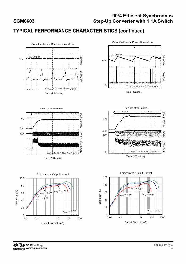
0
20
40
60
80
100
0.01 0.1 1 10 100 1000
Effic
ienc
y (%
)
Output Current (mA)
Efficiency vs. Output Current
VOUT = 3.3V
VCC = 2.4V VCC = 0.9V
VCC = 1.8V
Output Voltage in Discontinuous Mode
10mV/div 20m
A/div
Time (400ns/div)
VOUT
IL
VIN = 1.2V, RL = 3.3kΩ, VOUT = 3.3V
AC Coupled
Start-Up after Enable 2V/div 2V/div 5V/div 200m
A/div
Time (200μs/div)
Start-Up after Enable
5V/div 2V/div 5V/div 200mA/div
Time (200μs/div)
EN
VOUT
SW
IL
VIN = 2.4V, RL = 33Ω, VOUT = 3.3V
EN
VOUT
SW
IL
VIN = 3.6V, RL = 50Ω, VOUT = 5V
Output Voltage in Power-Save Mode
50mV/div 50m
A/div
Time (40μs/div)
VOUT
IL VIN = 3.6V, RL = 2.5kΩ, VOUT = 5.0V
AC Coupled

90% Efficient Synchronous SGM6603 Step-Up Converter with 1.1A Switch
8 FEBRUARY 2018 SG Micro Corp
www.sg-micro.com
TYPICAL PERFORMANCE CHARACTERISTICS (continued)
0
20
40
60
80
100
0.01 0.1 1 10 100 1000
Effic
ienc
y (%
)
Output Current (mA)
Efficiency vs. Output Current
VCC = 2.4V
VOUT = 5V
VCC = 1.8V
VCC = 3.6V

90% Efficient Synchronous SGM6603 Step-Up Converter with 1.1A Switch
9 FEBRUARY 2018 SG Micro Corp
www.sg-micro.com
TYPICAL APPLICATION CIRCUITS
SW
VCC
EN
VOUT
FB
C12×4.7μF
R1
R2
VCCBoost Output
SGM6603Power Supply
1
6
34
5
L14.7μH
GND2
C210μF
Figure 2. Power Supply Solution for Maximum Output Power Operating from a Single or Dual Alkaline Cell
SW
VCC
EN
VOUT
FB
C14.7μF
R1
R2
VCCBoost Output
SGM6603Power Supply
1
6
34
5
L14.7μH
GND2
C210μF
Figure 3. Power Supply Solution Having Small Total Solution Size
SW
VCC
EN
VOUT
FB
C14.7μF SGM6603Power
Supply
1
6
3
L14.7μH
GND2
C210μF
R1
LED CurrentUp to 30mAD1
4
5
Figure 4. Power Supply Solution for Powering White LEDs in Lighting Applications

90% Efficient Synchronous SGM6603 Step-Up Converter with 1.1A Switch
10 FEBRUARY 2018 SG Micro Corp
www.sg-micro.com
TYPICAL APPLICATION CIRCUITS (continued)
SW
VCC
EN
VOUT
FB
C12×4.7μF
R1
R2
VCCBoost Output
SGM6603Power Supply
1
6
34
5
L14.7μH
GND2
C210μF
C30.1µF
C41µF
DS1
VCC2 ~ 2×VCCUnregulatedAuxiliary Output
Figure 5. Power Supply Solution with Auxiliary Positive Output Voltage
SW
VCC
EN
VOUT
FB
C12×4.7μF
R1
R2
VCCBoost Output
SGM6603Power Supply
1
6
34
5
L14.7μH
GND2
C210μF
C30.1µF
C41µF
DS1
VCC2 ~ -VCCUnregulatedAuxiliary Output
Figure 6. Power Supply Solution with Auxiliary Negative Output Voltage

90% Efficient Synchronous SGM6603 Step-Up Converter with 1.1A Switch
11 FEBRUARY 2018 SG Micro Corp
www.sg-micro.com
TYPICAL APPLICATION CIRCUITS (continued)
VOUT 3.3V
SW
VCC
EN
VOUT
NC
C110μF
SGM6603-3.3Power Supply
1
6
3 4
5
L14.7μH
GND2
C210μF
Figure 7a. Basic Application Circuit for the Fixed Output Versions
SW
VCC
EN
VOUT
NC
C110μF
VOUT5.0V
SGM6603-5.0Power Supply
1
6
3 4
5
L14.7μH
GND2
C210μF
Figure 7b. Basic Application Circuit for the Fixed Output Versions

90% Efficient Synchronous SGM6603 Step-Up Converter with 1.1A Switch
12 FEBRUARY 2018 SG Micro Corp
www.sg-micro.com
APPLICATION INFORMATION Design Procedure The SGM6603 DC/DC converter is intended for systems powered by a single-cell, up to triple-cell alkaline, NiCd, and NiMH battery with a typical terminal voltage between 0.9V and 5.5V. It can also be used in systems powered by one-cell Li-Ion or Li-Polymer with a typical voltage between 2.5V and 4.2V. Programming Output Voltage In Figure 1, the output voltage of the SGM6603 DC/DC converter can be adjusted with an external resistor divider. The typical value of the voltage at the FB pin is 500mV. The maximum recommended value for the output voltage is 5.5V. R1 and R2 are calculated using Equation 1:
R1 = R2 ×( 1VV
FB
OUT − )= R2 × ( 1Vm500
VOUT − ) (1)
R2 is recommended to be 100kΩ. For example, if an output voltage of 3.3V is needed, a 560kΩ resistor should be chosen for R1. Inductor Selection A boost converter normally requires two main passive components for storing energy during the conversion. A boost inductor and a storage capacitor at the output are required. To select the boost inductor, it is recommended to keep the possible peak inductor current below the current limit threshold of the power switch in the chosen configuration. The highest peak current through the inductor and the switch depends on the output load, the input (VCC), and the output voltage (VOUT). Estimation of the maximum average inductor current is done using Equation 2:
IL = IO × 8.0V
V
CC
OUT
× (2)
For example, for an output current of 75mA at 3.3V, at least an average current of 340mA flows through the inductor at a minimum input voltage of 0.9V.
The second parameter for choosing the inductor is the desired current ripple in the inductor. Normally, it is advisable to work with a ripple of less than 20% of the average inductor current. A smaller ripple reduces the magnetic hysteresis losses in the inductor, as well as output voltage ripple and EMI. But in the same way, regulation time rises at load changes. In addition, a larger inductor increases the total system costs. With these parameters, it is possible to calculate the value for the inductor by using Equation 3:
L = OUTL
CCOUTCC
VfIΔ)VV(V
××−×
(3)
Parameter f is the switching frequency and ΔIL is the ripple current in the inductor. In typical applications, a 4.7µH inductance is recommended. The device has been optimized to operate with inductance values between 2.2µH and 10µH. Nevertheless, operation with higher inductance values may be possible in some applications. Detailed stability analysis is then recommended. Care must be taken because load transients and losses in the circuit can lead to higher currents as estimated in Equation 3. Also, the losses in the inductor which include magnetic hysteresis losses and copper losses are a major parameter for total circuit efficiency. Input Capacitor At least a 10µF input capacitor is recommended to improve transient behavior of the regulator and EMI behavior of the total power supply circuit. A ceramic capacitor or a tantalum capacitor with a 100nF ceramic capacitor in parallel, placed close to the IC, is recommended.

90% Efficient Synchronous SGM6603 Step-Up Converter with 1.1A Switch
13 FEBRUARY 2018 SG Micro Corp
www.sg-micro.com
APPLICATION INFORMATION (continued) Output Capacitor The major parameter necessary to define the output capacitor is the maximum allowed output voltage ripple of the converter. This ripple is determined by two parameters of the capacitor, the capacitance and the ESR. It is possible to calculate the minimum capacitance needed for the defined ripple, supposing that the ESR is zero, by using Equation 4:
CMIN = OUT
CCOUTO
VVΔf)VV(I
××−×
(4)
Parameter f is the switching frequency and ΔV is the maximum allowed ripple.
With a chosen ripple voltage of 10mV, a minimum capacitance of 4.5µF is needed. In this value range, ceramic capacitors are a good choice. The ESR and the additional ripple created are negligible. It is calculated using Equation 5:
ΔVESR = IO × RESR (5)
The total ripple is the sum of the ripple caused by the capacitance and the ripple caused by the ESR of the capacitor. Additional ripple is caused by load transients. This means that the output capacitor has to completely supply the load during the charging phase of the inductor.
The value of the output capacitance depends on the speed of the load transients and the load current during the load change. With the calculated minimum value of 4.5µF and load transient considerations, the recommended output capacitance value is in the range of 4.7μF to 22µF.
Care must be taken on capacitance loss caused by derating due to the applied DC voltage and the frequency characteristic of the capacitor. For example, larger form factor capacitors (in 1206 size) have their self resonant frequencies in the same frequency range as the SGM6603 operating frequency. So the effective capacitance of the capacitors used may be significantly lower. Therefore, the recommendation is to use smaller capacitors in parallel instead of one larger capacitor.
Layout Considerations As for all switching power supplies, the layout is an important step in the design, especially at high-peak currents and high switching frequencies. If the layout is not carefully done, the regulator could show stability problems as well as EMI problems. Therefore, use wide and short traces for the main current path and for the power ground tracks. The input capacitor, output capacitor, and the inductor should be placed as close as possible to the IC. Use a common ground node for power ground and a different one for control ground to minimize the effects of ground noise. Connect these ground nodes at any place close to the ground pin of the IC.
The feedback divider should be placed as close as possible to the ground pin of the IC. To lay out the control ground, it is recommended to use short traces as well, separated from the power ground traces. This avoids ground shift problems, which can occur due to superimposition of power ground current and control ground current. Thermal Information Implementation of integrated circuits in low-profile and fine-pitch surface-mount packages typically requires special attention to power dissipation. Many system-dependent issues such as thermal coupling, airflow, added heat sinks and convection surfaces, and the presence of other heat-generating components affect the power-dissipation limits of a given component.
Three basic approaches for enhancing thermal performance follow.
1. Improving the power dissipation capability of the PCB design. 2. Improving the thermal coupling of the component to the PCB. 3. Introducing airflow in the system.

90% Efficient Synchronous SGM6603 Step-Up Converter with 1.1A Switch
14 FEBRUARY 2018 SG Micro Corp
www.sg-micro.com
REVISION HISTORY NOTE: Page numbers for previous revisions may differ from page numbers in the current version. FEBRUARY 2018 ‒ REV.A.2 to REV.A.3
Update the Typical Performance Characteristics Efficiency vs. Input Voltage (VOUT = 3.3V, VOUT = 5.0V) ........................................................................................................................................ 5
APRIL 2015 ‒ REV.A.1 to REV.A.2
Update the Electrical Characteristics VIH (0.9V ≤ VCC ≤ 1.8V) 1.5V - 0.8VCC ................................................................................................................................................................... 4
JANUARY 2015 ‒ REV.A to REV.A.1
Update the Electrical Characteristics Switch Current Limit ............................................................................................................................................................................................ 4 Add dot on pin 1 SOT-23-6 ............................................................................................................................................................................ 3, 14
Changes from Original (JANUARY 2013) to REV.A
Changed from product preview to production data ............................................................................................................................................. All

PACKAGE INFORMATION
TX00034.000 SG Micro Corp www.sg-micro.com
PACKAGE OUTLINE DIMENSIONS SOT-23-6
Symbol Dimensions
In Millimeters Dimensions
In Inches MIN MAX MIN MAX
A 1.050 1.250 0.041 0.049 A1 0.000 0.100 0.000 0.004 A2 1.050 1.150 0.041 0.045 b 0.300 0.500 0.012 0.020 c 0.100 0.200 0.004 0.008 D 2.820 3.020 0.111 0.119 E 1.500 1.700 0.059 0.067
E1 2.650 2.950 0.104 0.116 e 0.950 BSC 0.037 BSC
e1 1.900 BSC 0.075 BSC L 0.300 0.600 0.012 0.024 θ 0° 8° 0° 8°
EE1
e
e1
b
D
A1
A2
A
c
L
θ0.2
2.59
0.99
0.950.69
RECOMMENDED LAND PATTERN (Unit: mm)

PACKAGE INFORMATION
TX10000.000 SG Micro Corp
www.sg-micro.com
TAPE AND REEL INFORMATION NOTE: The picture is only for reference. Please make the object as the standard.
KEY PARAMETER LIST OF TAPE AND REEL
Package Type Reel Diameter
Reel Width W1
(mm) A0
(mm) B0
(mm) K0
(mm) P0
(mm) P1
(mm) P2
(mm) W
(mm) Pin1
Quadrant
DD0001 SOT-23-6 7″ 9.5 3.17 3.23 1.37 4.0 4.0 2.0 8.0 Q3
Reel Width (W1)
Reel Diameter
REEL DIMENSIONS
TAPE DIMENSIONS
DIRECTION OF FEED
P2 P0
W
P1 A0 K0
B0Q1 Q2
Q4Q3 Q3 Q4
Q2Q1
Q3 Q4
Q2Q1

PACKAGE INFORMATION
TX20000.000 SG Micro Corp
www.sg-micro.com
CARTON BOX DIMENSIONS NOTE: The picture is only for reference. Please make the object as the standard.
KEY PARAMETER LIST OF CARTON BOX
Reel Type Length (mm)
Width (mm)
Height (mm) Pizza/Carton
DD0002
7″ (Option) 368 227 224 8
7″ 442 410 224 18
Recommended