MDLNTHU
Outline
1 Introduction
2 Basic IC fabrication processes
3 Fabrication techniques for MEMS
4 Applications
5 Mechanics issues on MEMS
MDLNTHU
2. Basic IC fabrication processes
2.2 Photolithography
2.3 Etching
2.1 Deposition and growth
2.4 Bonding

MDLNTHU
2.1 Deposition and growth
• Deposition and growth are the processes to produce a thin film on the surface of substrate
• Deposition vs Growth
substrste
substrste substrsteth
th-Δh

MDLNTHU
• Two approaches for deposition
+ Physical vapor deposition (PVD)
+ Chemical vapor deposition (CVD)
EvaporationSputtering
LPCVDPECVD
MDLNTHU
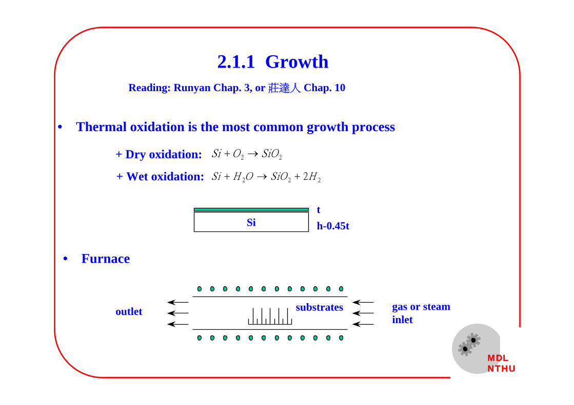
2.1.1 Growth Reading: Runyan Chap. 3, or 莊達人 Chap. 10
• Thermal oxidation is the most common growth process
• Furnace
gas or steam inlet
outlet
+ Dry oxidation:
+ Wet oxidation:
Si O SiO+ →2 2
Si H O SiO H+ → +2 2 22
Sith-0.45t
substrates
MDLNTHU
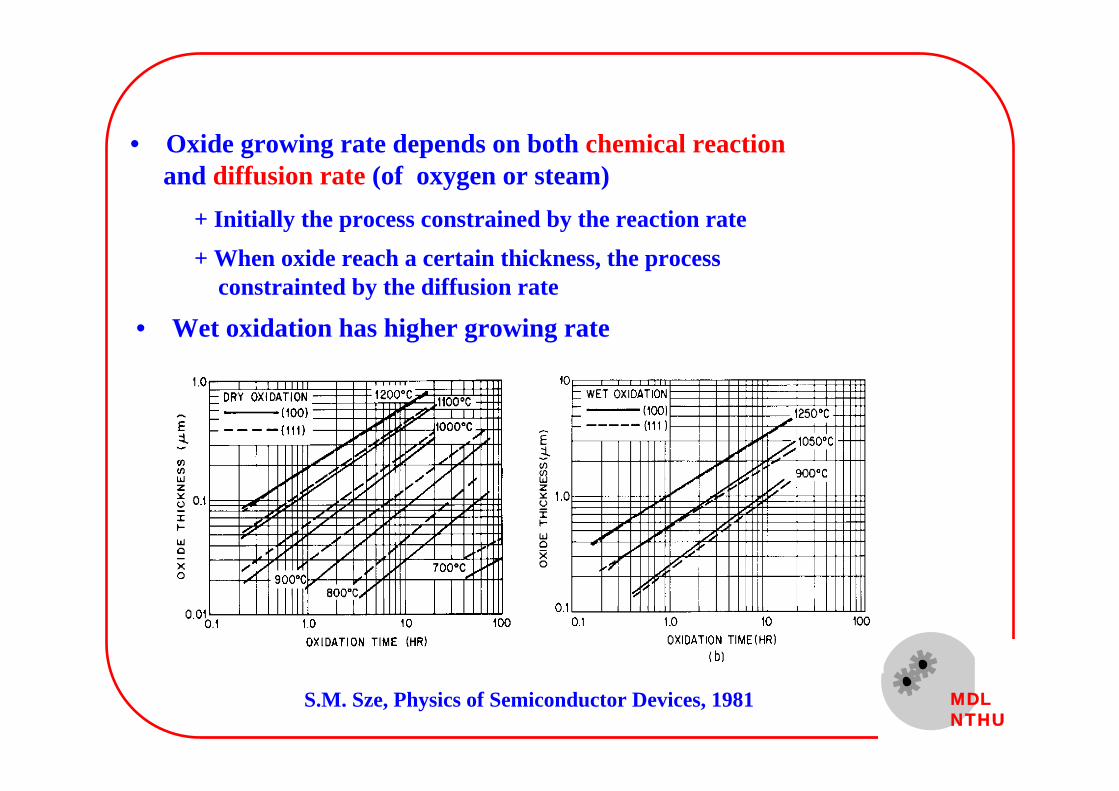
• Wet oxidation has higher growing rate
• Oxide growing rate depends on both chemical reactionand diffusion rate (of oxygen or steam)
+ Initially the process constrained by the reaction rate+ When oxide reach a certain thickness, the process
constrainted by the diffusion rate
S.M. Sze, Physics of Semiconductor Devices, 1981

MDLNTHU
• Thermal residual stress induced by the difference of thermal expansion coefficients between substrate and thin films
thin filmhigh temperature(inside the furnace)
low temperature(outside the furnace)
ε = ΔαΔTResidual strain
Thermal expansion coefficient
Temperature
substrste
substrste
substrste
substrste

MDLNTHU
• Effect of oxidation temperature on oxide density
• Effect of growing process on oxide Young's modulus
57 GPa (wet)67 GPa (dry)
60 GPa (20% dry and 80% wet)
K.E. Petersen and C.R. Guarnieri, J. Applied Physics, 1979.
W. Fang and J.A. Wickert, DSSC Annual report, Carnegie Mellon University, 1992.
Temperature(C) Density
60070080090010001150
2.2862.2652.2532.2362.2242.208
E.A. Irene et al., J. Electrochemical Society, 1982.

MDLNTHU
• Advantage : easy to operate and inexpensive good quality
• Disadvantage : high operating temperature
time consumingthermal residual stress
• Silicon nitride can be grown through the same mechanism, howeverthe growing temperature is too high
3 2 2 3 4Si N Si N+ →
MDLNTHU
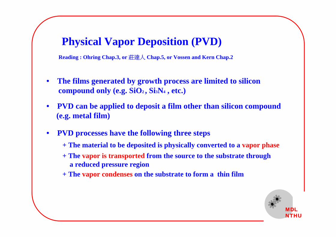
• PVD can be applied to deposit a film other than silicon compound(e.g. metal film)
Physical Vapor Deposition (PVD)
• The films generated by growth process are limited to silicon compound only (e.g. SiO2 , Si3N4 , etc.)
• PVD processes have the following three steps+ The material to be deposited is physically converted to a vapor phase+ The vapor is transported from the source to the substrate through
a reduced pressure region+ The vapor condenses on the substrate to form a thin film
Reading : Ohring Chap.3, or 莊達人 Chap.5, or Vossen and Kern Chap.2
MDLNTHU
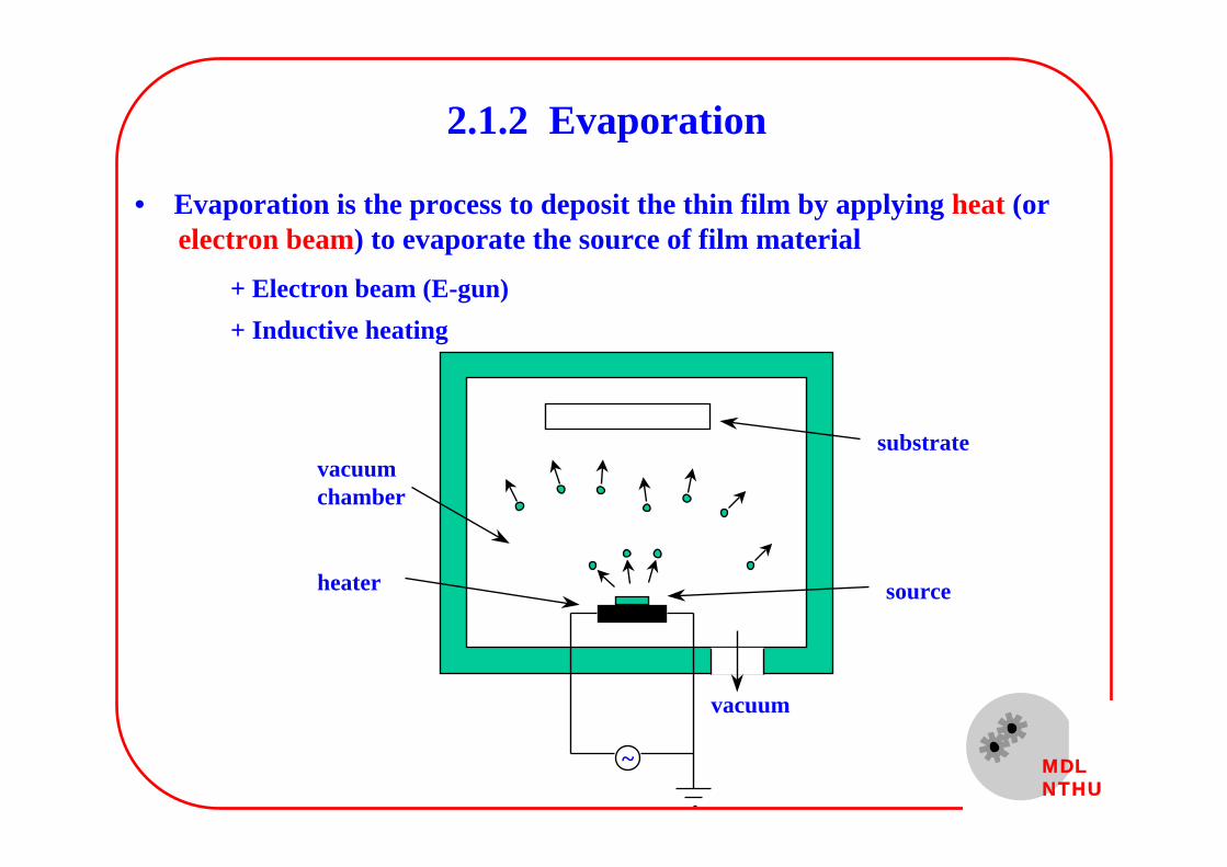
2.1.2 Evaporation
• Evaporation is the process to deposit the thin film by applying heat (or electron beam) to evaporate the source of film material
+ Electron beam (E-gun)+ Inductive heating
~
vacuum
substrate
sourceheater
vacuumchamber

MDLNTHU
S.M. Sze, Semiconductor devices, 1985

MDLNTHU
Deposition Mechanism• The vapor deposits on the substrate through five steps
(a) Nucleation(b) Nuclei growth(c) Coalescence(d) Filling of channels(e) Film growth
L. Eckertova and T. Ruzicka, Diagnostics and Applications of Thin Films, 1993.
MDLNTHU
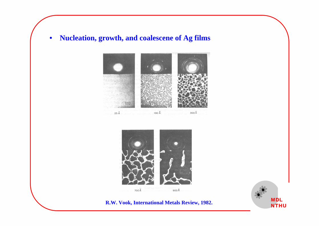
• Nucleation, growth, and coalescene of Ag films
R.W. Vook, International Metals Review, 1982.

MDLNTHU
• Nucleation
• Free energy of particles
+ Surface energy:
+ Volume energy:
+ Free energy of particle: surface energy + volume energy
r0
r1
subtrate
4 2πr A⋅
4
33πr B⋅
MDLNTHU
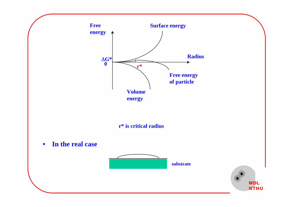
• In the real case
Free energy
Surface energy
Volume energy
Radius
Free energy of particle
r* is critical radius
r*ΔG*
0
substrate

MDLNTHU
Advantages
• High deposition rate (e.g. 0.5 μm/min for Al)
• The low energy of the impinging metal atoms onto the substrate leaves the substrate surface undamaged
• Due to high vacuum environment, less residual gas will be incorporated in the deposited film

MDLNTHU
Disadvantages
• It is difficult to deposit multicomponent (e.g. AlCu) by evaporation, since their vapor pressure are different
• It is necessary to operate vaporation process in higher vacuum environment to prevent collision between evaporant and gas molecules
• It is difficult to melt high melting point material(need electron beam to complete the processes)
• Poor step coverage
MDLNTHU
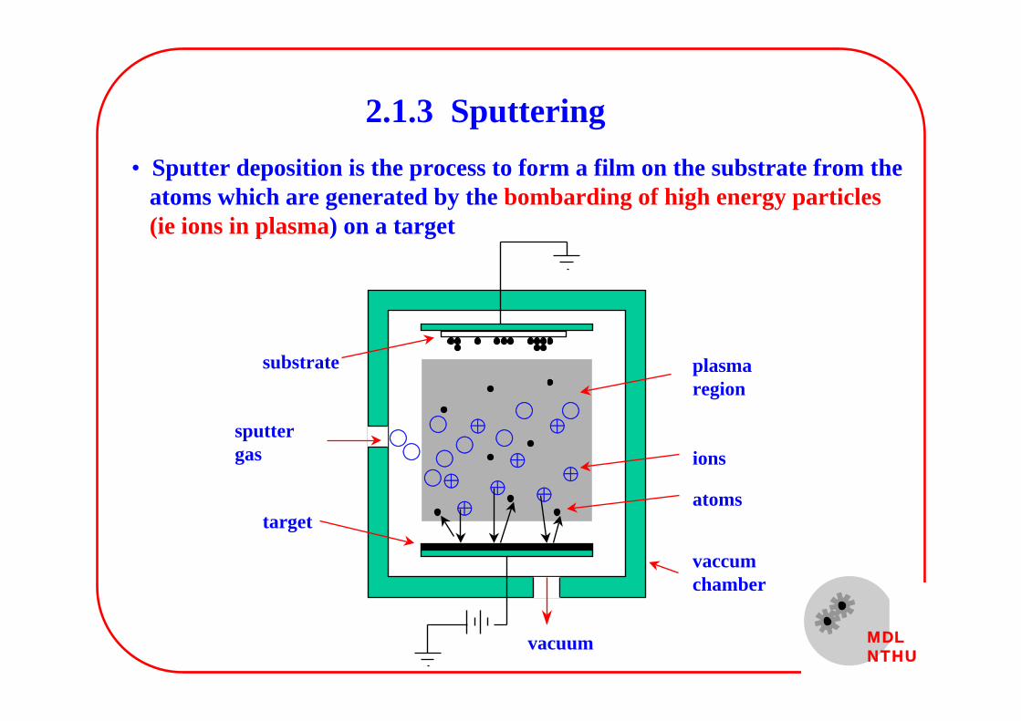
2.1.3 Sputtering • Sputter deposition is the process to form a film on the substrate from the
atoms which are generated by the bombarding of high energy particles (ie ions in plasma) on a target
vacuum
○○
♁ ♁
♁♁
♁
♁♁ ♁
○
○○
○
○○
○
sputter gas ions
atomstarget
vaccumchamber
plasma region
substrate
MDLNTHU
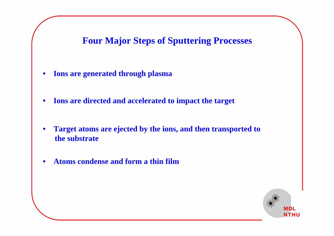
Four Major Steps of Sputtering Processes
• Ions are generated through plasma
• Ions are directed and accelerated to impact the target
• Target atoms are ejected by the ions, and then transported to the substrate
• Atoms condense and form a thin film
MDLNTHU
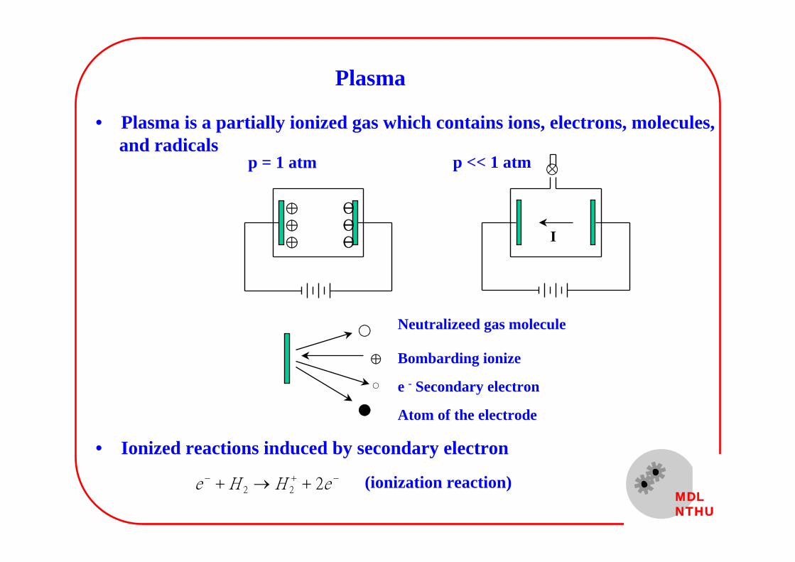
Plasma
• Plasma is a partially ionized gas which contains ions, electrons, molecules, and radicals
• Ionized reactions induced by secondary electron
(ionization reaction)
♁
♁♁
ΘΘΘ
♁I
○
●
♁
○
Neutralizeed gas molecule
Bombarding ionize
e - Secondary electron
Atom of the electrode
p = 1 atm p << 1 atm
e H H e− + −+ → +2 2 2

MDLNTHU
Plasma process
2. Add Ar gas and the chamber becomes low vacuum (usually arround 1 ~ 10m Torr)
3. Applied a high voltage to the electrode
4. A free electron existing in the electric field will be accelerated (this free electron is most likely created from Ar by a passing cosmic ray)
1. Clean the chamber by pumping it to high vacuum (< 10-6 Torr)
5. The accelerated electron will hit an Ar atom after traveling a distance (its mean free path)
6. If the electron has enough energy ( > 15.7 eV for Ar), this Ar atom will be ionized by releasing its electron
7. If the electron do not have enough energy, the orbital electron of this Ar atom will be excited to a higher energy state
MDLNTHU
8. When the number of free electron increased, the area between two electrode will reach a condition called gas break down and then current flows in the external circuit
More details can be found in :
(1) B. Chapman, Glow Discharge Processes, 1980.(2) J.L. Vossen and W. Kern (editors), Thin Film Processes, 1978.
9. The current will decay to zero unless there is a mechanism available for generating additional free electrons
10. In the mean time, the ions generated in step 6 will also hit the electrode (cathode) after accelerated in the electric field. Thus the cathode emits free electrons (secondary electron) when struck by ions
11. Finally, the current in step 8 is sustained by the free electron generated in step 10

MDLNTHU
• The most common gas for plasma is Argon (Ar)
+ Noble gas
+ Cost
+ Mass
• Excitation reactions induced by secondary electron
(excitation reaction)
(Ar* is excitated state)
e Ar Ar e− −+ → +*
Ar Ar h* → + υ
MDLNTHU
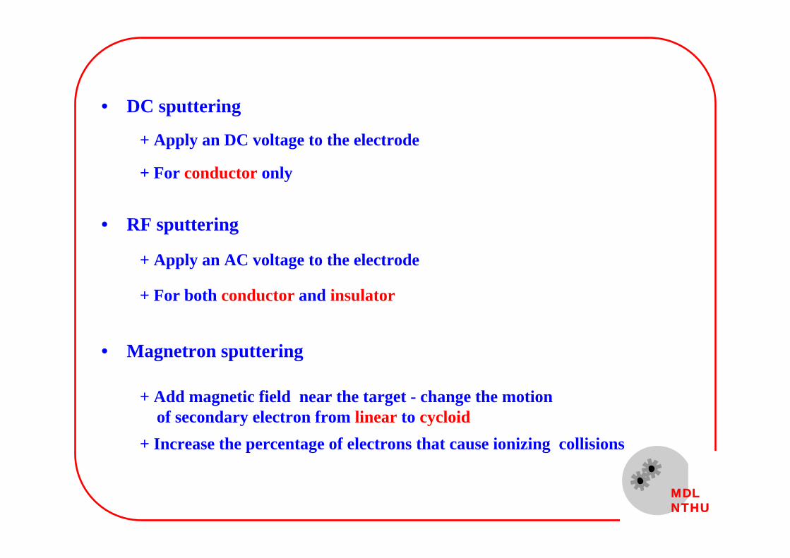
• DC sputtering
• RF sputtering
• Magnetron sputtering
+ Apply an DC voltage to the electrode
+ For conductor only
+ Apply an AC voltage to the electrode
+ For both conductor and insulator
+ Add magnetic field near the target - change the motion of secondary electron from linear to cycloid
+ Increase the percentage of electrons that cause ionizing collisions
MDLNTHU
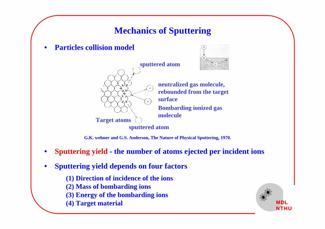
Mechanics of Sputtering
• Particles collision model
G.K. wehner and G.S. Anderson, The Nature of Physical Sputtering, 1970.
• Sputtering yield - the number of atoms ejected per incident ions
• Sputtering yield depends on four factors(1) Direction of incidence of the ions(2) Mass of bombarding ions(3) Energy of the bombarding ions(4) Target material
sputtered atom
sputtered atomTarget atoms
Bombarding ionized gas molecule
neutralized gas molecule, rebounded from the target surface

MDLNTHU
• Response and the kinetic energy of the ions
+ High energy (> 10 KeV) : the bombarding ions are most likely to be embedded in the target
+ Low energy (< 10 KeV) : reflection or absorption of the bombarding ions
+ Energy between the above two extremes : the energy of the bombarding ions is (1) transferred to the solid in the form of heat and crystal damage, and (2) ejected the atoms from the surface
• Sputtering is a low efficient process, after ion bombardment:
+ 70% of the ion energy becomes heat
+ 25% of the ion energy generating secondary electrons
+ only 2% of the ion energy used for sputtering process
MDLNTHU
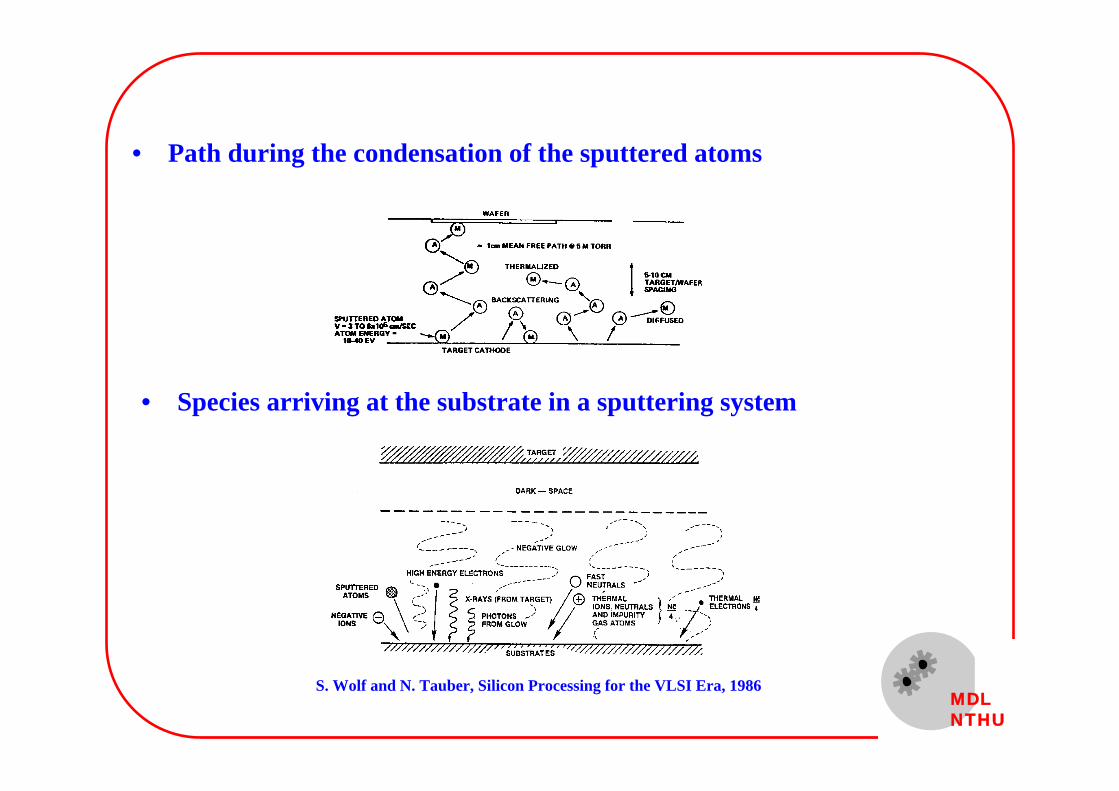
• Path during the condensation of the sputtered atoms
• Species arriving at the substrate in a sputtering system
S. Wolf and N. Tauber, Silicon Processing for the VLSI Era, 1986

MDLNTHU
Intrinsic residual stress
• Computer simulation of a film deposited by evaporation at different temperature
• Tensile residual stress due to the voids of the film
M. Ohring, The Material Science of Thin Films, 1992.
MDLNTHU
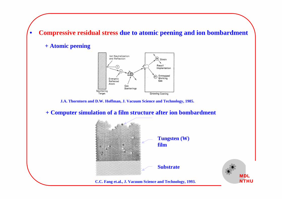
• Compressive residual stress due to atomic peening and ion bombardment
+ Atomic peening
+ Computer simulation of a film structure after ion bombardment
C.C. Fang et.al., J. Vacuum Science and Technology, 1993.
J.A. Thorntorn and D.W. Hoffman, J. Vacuum Science and Technology, 1985.
Tungsten (W) film
Substrate

MDLNTHU
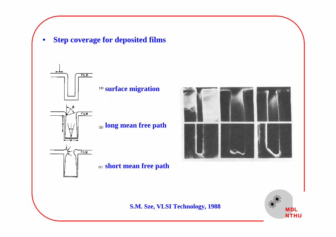
• If the surface of the substrate has a step structure, the thickness of the deposited film may not be uniform
Step coverage (%) : t/h×100%
Step coverage
• Step coverage is defined as the ratio of the minimum thickness of the film as it cross a step to the nominal thickness of the film on the flat region
stepnon-uniformfilm thickness
nominal filmthickness, h
uniform filmthickness
minimum filmthickness, t

MDLNTHU
+ height of the step
+ aspect ratio
+ the slope of the step
+ shape of the step
• Step coverage is determined by
+ deposition method
M. Ohring, The materials science of thin films, 1992
MDLNTHU
• Step coverage for deposited films
S.M. Sze, VLSI Technology, 1988
short mean free path
surface migration
long mean free path

MDLNTHU
+ heating the substrate can improve the step coverage
+ sputter etching the underlying substrate before deposition
+ optimize the target design
• Step coverage can be improved by the following approaches
+ bias sputtering
S. Wolf and N. Tauber, Silicon Processing for the VLSI Era, 1986

MDLNTHU
Advantages (vs evaporation)
• Uniform thickness over large substrates
• Control film thickness easily
• Control alloy composition
• Control step coverage, grain structure, stress by varying the deposition conditions
• Better adhesion

MDLNTHU
Disadvantages (vs evaporation)
• Expensive equipment
• Ion bombardment is critical to some materials (organic)
• More impurities due to lower vacuum
MDLNTHU
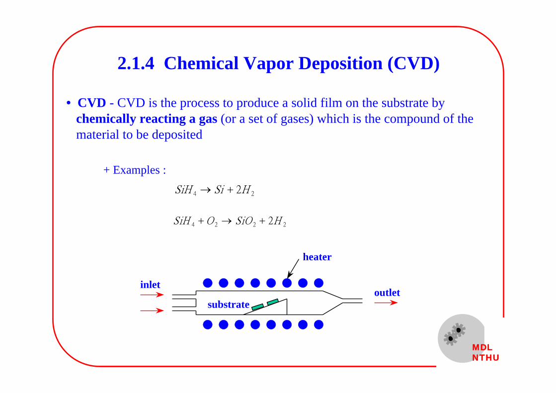
2.1.4 Chemical Vapor Deposition (CVD)
• CVD - CVD is the process to produce a solid film on the substrate by chemically reacting a gas (or a set of gases) which is the compound of the material to be deposited
+ Examples :SiH Si H4 22→ +
SiH O SiO H4 2 2 22+ → +
substrate
inletoutlet
● ● ● ● ● ● ● ●
● ● ● ● ● ● ● ●
heater

MDLNTHU
• The reactants are transported onto the substrate surface
• The reactants are adsorbed on the substrate surface
• A chemical reaction takes place on the surface leading to the formation of the film and reaction products
• The reaction products are desorbed from the substrate surface
• The reaction products are transported away from the substrate surface
Five Basic Steps of CVD Processes

MDLNTHU
• The deposition rate is determined by (1) surface reaction rate, or (2)mass transportation rate
• Since the five steps of CVD process are sequential, the one with slowest rate will determine the deposition rate
+ surface reaction rate, R = K0C1e-E1/kT
Deposition Rate
+ mass transportation rate, R = DC2e-E2 /kT
mass transport limited regime
surface reaction limited regime
Dep
ositi
on r
ate,
log
(R)
Temperature, 1/T
MDLNTHU
• Mass transport limited regime
+ high temperature (compare with surface reaction regime)
+ Need to control the flux of reactant to insure films with uniform thickness
+ poor thickness uniformity
• Surface reaction rate limited regime
+ low temperature (compare with mass transport regime)
+ Need to control temperature well
+ better thickness uniformity

MDLNTHU
• Atmospheric pressure CVD (APCVD)
Three most common CVD process
+ APCVD is CVD process operating at atmospheric pressure
+ Conducted in mass transporation limited regime - the reactant flux to all parts of every substrate in the reactor must be controlled
VLSI Technology edited by S.M. Sze, 1988.
substrate
inletoutlet
● ● ● ● ● ● ● ●
● ● ● ● ● ● ● ●
heater

MDLNTHU
• Low pressure CVD (LPCVD)
+ LPCVD is CVD process operating at medium vacuum (0.25 ~ 2.0 torr) and higher temperature (550 ~ 600 C)
+ Conducted in surface reaction rate limited regime
+ Better thickness uniformity - temperature control is relatively easy to achieve (compare with flux control)
+ Higher wafer capacity - less restriction on the location of the substrate
VLSI Technology edited by S.M. Sze, 1988.
+ Less particulate contamination - gas phase reaction is reduced by low pressure

MDLNTHU
• Plasma enhanced CVD (PECVD)
+ PECVD uses both the thermal energy and RF-induced plasma to transfer energy into the reactant gases
+ Conducted in surface reaction rate limited regime
+ Residual stresses can be adjusted by ion bombardment
+ Deposited film is contaminated by by-products
VLSI Technology edited by S.M. Sze, 1988.

MDLNTHU
Process Advantages Disadvantages Applications
APCVD
LPCVD
PECVD
Simple reactorFast depositionLow temperature
Chemical and particulate contamination
Excellent purity, uniformity, and step coverageLarge wafer capacity
Poor step coverageParticulate contamination
OxidePolysiliconSilicon Nitride
Low temperatureFast depositionGood step coverage
Oxide
MetalsSilicon Nitride
High temperatureLow deposition
• Summary of three major CVD processes
S. Wolf and R.N. Tauber, Silicon Processing for the VLSI Era Vol.1, 1986
MDLNTHU
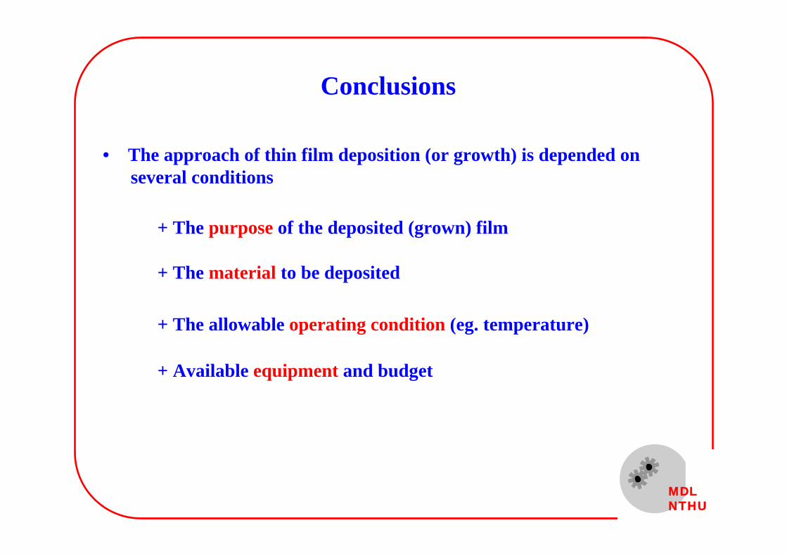
Conclusions
• The approach of thin film deposition (or growth) is depended on several conditions
+ The allowable operating condition (eg. temperature)
+ Available equipment and budget
+ The purpose of the deposited (grown) film
+ The material to be deposited

MDLNTHU
Place Structure material
Spacer material
Surface material
UC-Berkeley
MIT
Stanford
Carnegie Mellon
Nissan
polysilicon
polysilicon
polysilicon
aluminum
aluminum
oxide
oxide
oxide
silicon nitride
silicon nitride
silicon nitride
oxide and aluminum bulk silicon bulk silicon
polymide
• The MEMS materials used in different places
substratesurface
spacer
structure
MDLNTHU
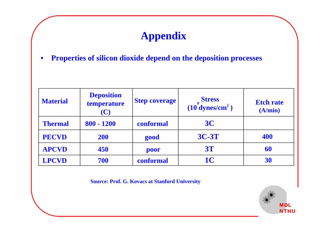
Appendix
MaterialDeposition
temperature(C)
Step coverage Stress(10 dynes/cm )
Etch rate (A/min)
9 2
Thermal
PECVD
APCVDLPCVD
800 - 1200
200
450700
400
6030
3C
3C-3T3T1C
conformal
conformal
good
poor
• Properties of silicon dioxide depend on the deposition processes
Source: Prof. G. Kovacs at Stanford University
MDLNTHU
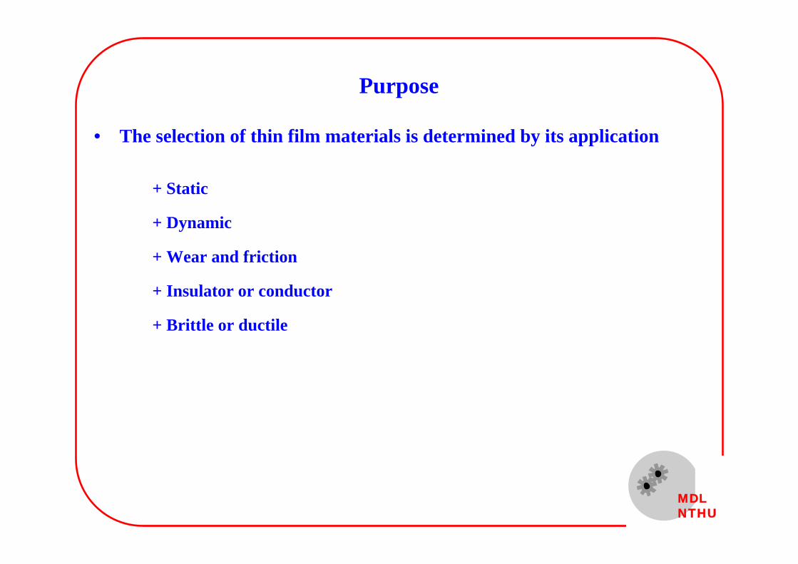
Purpose
• The selection of thin film materials is determined by its application
+ Static
+ Dynamic
+ Wear and friction
+ Insulator or conductor
+ Brittle or ductile

MDLNTHU
Materials for Thin Film Structures
• Typical materials semiconductor
+ aluminum alloy (AlCu, etc.)+ polycrystalline silicon (polysilicon, or poly)+ silicon nitride (Si3N4)
+ silicon (Si)+ silicon dioxide (SiO2)
• Metals
+ others+ nickel (Ni)+ gold (Au)
+ titanium (Ti)+ tungsten (W)
• Active films
+ aluminum nitride (AlN)+ shape memory alloy (TiNi)
+ lead-zirconate-titanate (PZT)+ zinc oxide (ZnO)
MDLNTHU
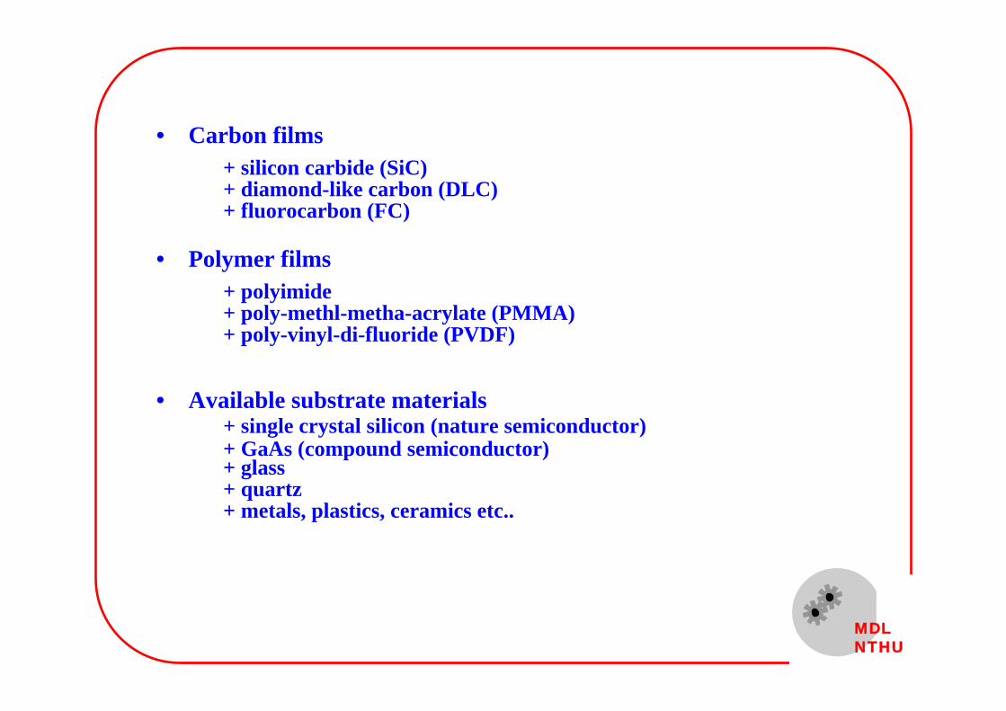
• Carbon films
+ fluorocarbon (FC)
+ silicon carbide (SiC)+ diamond-like carbon (DLC)
• Polymer films
+ poly-vinyl-di-fluoride (PVDF)
+ polyimide+ poly-methl-metha-acrylate (PMMA)
• Available substrate materials
+ glass+ quartz
+ single crystal silicon (nature semiconductor)+ GaAs (compound semiconductor)
+ metals, plastics, ceramics etc..

MDLNTHU
Material Properties for Thin Films
• Mechanical properties
+ Thermal expansion coeff.+ Yield stress+ Hardness
+ Young's modulus+ Density
• Electrical properties (for your reference)
+ Thermal conductivity
+ atoms/volume+ Hole mobility+ Electron mobility
+ Resistivity+ Dielectric constant
+ Energy gap at 300 K o

MDLNTHU
• Mechanical properties of some basic thin film materials• These mechanical properties may depend on the deposition processes
Source: Prof. G. Kovacs at Stanford University
MaterialThermal
expansion coefficient
(10 /K)
Young's modulus
(10 N/m )
Thermal conductivity
(W/mK)
Si
SiO2
Si3N4
Polysilicon
Polyimide
Density (10 kg/m )2
3
Al
Au
Ni
311
-6
2.6 1.62 149 2.42
0.40.67 (dry)0.57 (wet)0.7 (bulk)
1.4 2.66
2.8 1.46 (CVD)1.3 (sputtered) 18.5 3.0
2.33
20-70 0.03 0.167
23.0 0.69 237 2.692
14.3 0.8 318 19.4
12.8 2.1 90.9 9.04

MDLNTHU
• Comparison of the mechanical properties of some basic semiconductor materials and mechanical materials
Source: K.E. Petersen, Proceeding of the IEEE, 1982.
Thermal conductivity
(W/mK)
Si SiO2 Si3N4Al
Density (10 kg/m )33
Young's modulus
(10 N/m )211
Thermal expansion coefficient
(10 /K)-6
Yield strength
(10 N/m )29
Material Steel Stainless steel
Knoophardness (Kg/mm )2
2.1
4.2
7.9
0.97
12
1500
2.0
2.1
7.9
0.33
17.3
660
0.7
0.17
2.7
2.36
25
130
1.9
7
2.3
1.57
2.33
850
0.73
8.4
2.5
0.014
0.55
820
3.85
14
3.1
0.19
0.8
3500
Recommended