COMPUTER ORGANIZATION
INDEX
UNIT-II PPT SLIDESSrl. No. Module as per Session planner Lecture No. PPT Slide No.
1. Register Transfer language
2. Register Transfer Bus and memory transfers
3. Arithmetic Micro-operations
4. Logic micro operations
5. Shift micro operations
6. Arithmetic logic shift unit
7. Instruction codes
8. Computer registers
9. Computer instructions
10. Instruction cycle
11. Reference Instructions
12. Input-output and Interrupt
13. STACK organization
14. Instruction formats
15. Addressing modes
16. DATA Transfer and manipulation
17. Program control
18. Reduced Instruction Set Computer
REGISTER TRANSFER LANGUAGE
• Combinational and sequential circuits can be used to create simple digital systems.
• These are the low-level building blocks of a digital computer.
• Simple digital systems are frequently characterized in terms of– the registers they contain, and– the operations that they perform.
• Typically,– What operations are performed on the data in the registers– What information is passed between registers
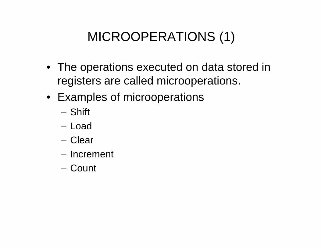
MICROOPERATIONS (1)
• The operations executed on data stored in registers are called microoperations.
• Examples of microoperations– Shift– Load– Clear– Increment– Count
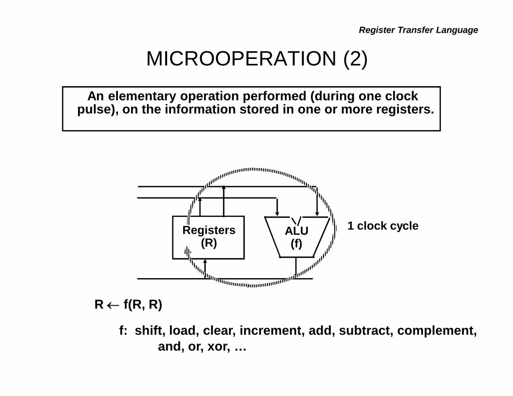
MICROOPERATION (2)
An elementary operation performed (during one clock pulse), on the information stored in one or more registers.
R f(R, R)
f: shift, load, clear, increment, add, subtract, complement,and, or, xor, …
ALU(f)
Registers(R)
1 clock cycle
Register Transfer Language
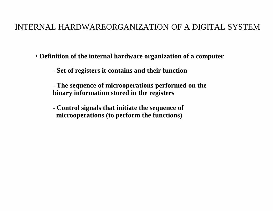
INTERNAL HARDWAREORGANIZATION OF A DIGITAL SYSTEM
- Set of registers it contains and their function
- The sequence of microoperations performed on the binary information stored in the registers
- Control signals that initiate the sequence of microoperations (to perform the functions)
• Definition of the internal hardware organization of a computer
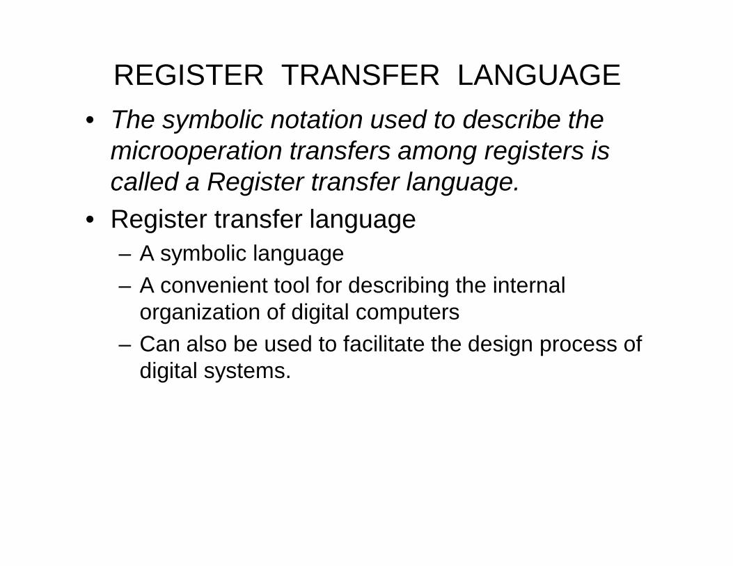
REGISTER TRANSFER LANGUAGE• The symbolic notation used to describe the
microoperation transfers among registers is called a Register transfer language.
• Register transfer language– A symbolic language– A convenient tool for describing the internal
organization of digital computers– Can also be used to facilitate the design process of
digital systems.
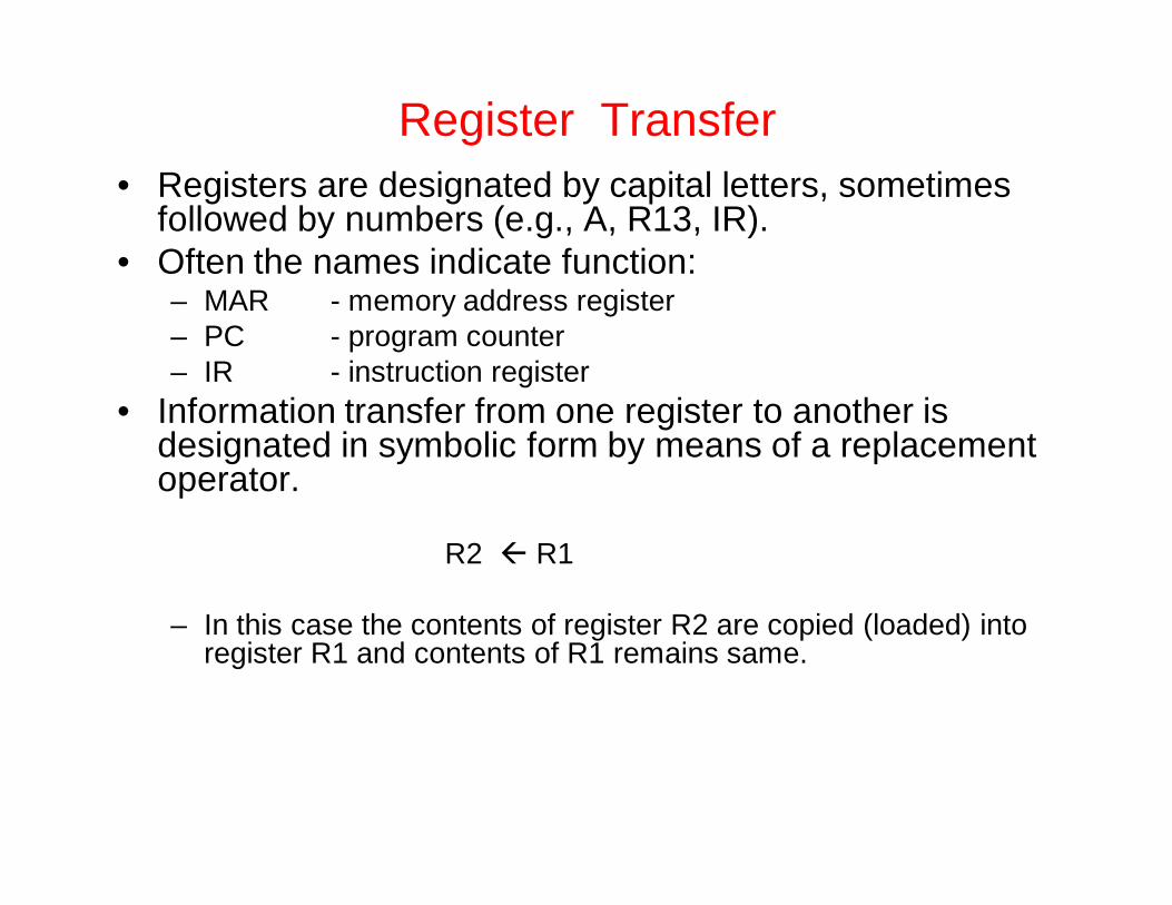
Register Transfer• Registers are designated by capital letters, sometimes
followed by numbers (e.g., A, R13, IR).• Often the names indicate function:
– MAR - memory address register– PC - program counter– IR - instruction register
• Information transfer from one register to another is designated in symbolic form by means of a replacement operator.
R2 R1
– In this case the contents of register R2 are copied (loaded) into register R1 and contents of R1 remains same.
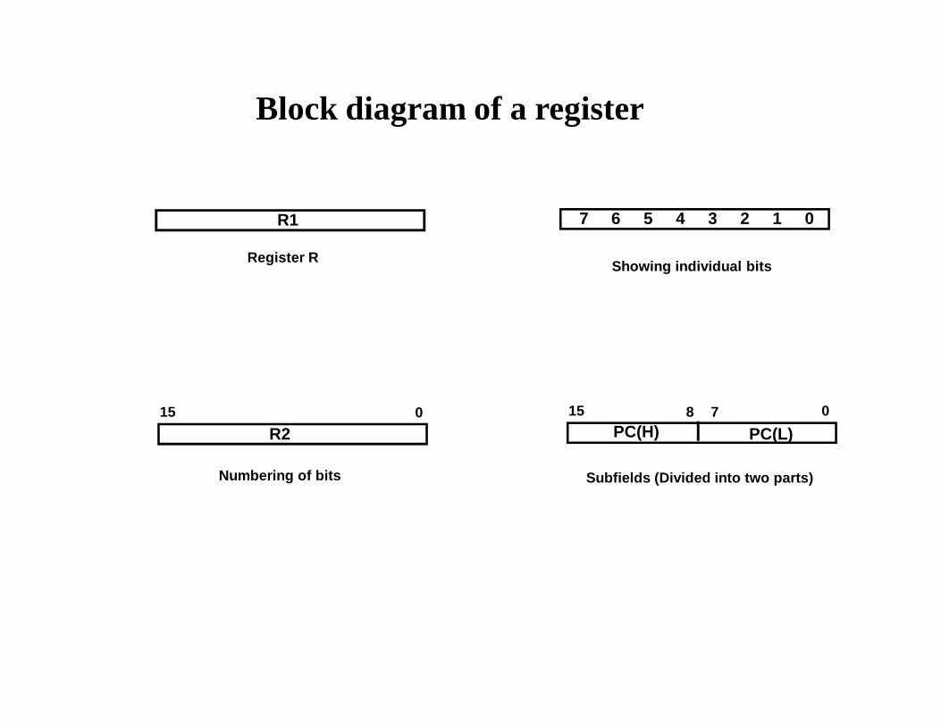
R1
Register R
Numbering of bits
Showing individual bits
Subfields (Divided into two parts)
PC(H) PC(L)15 8 7 0
Block diagram of a register
7 6 5 4 3 2 1 0
R215 0
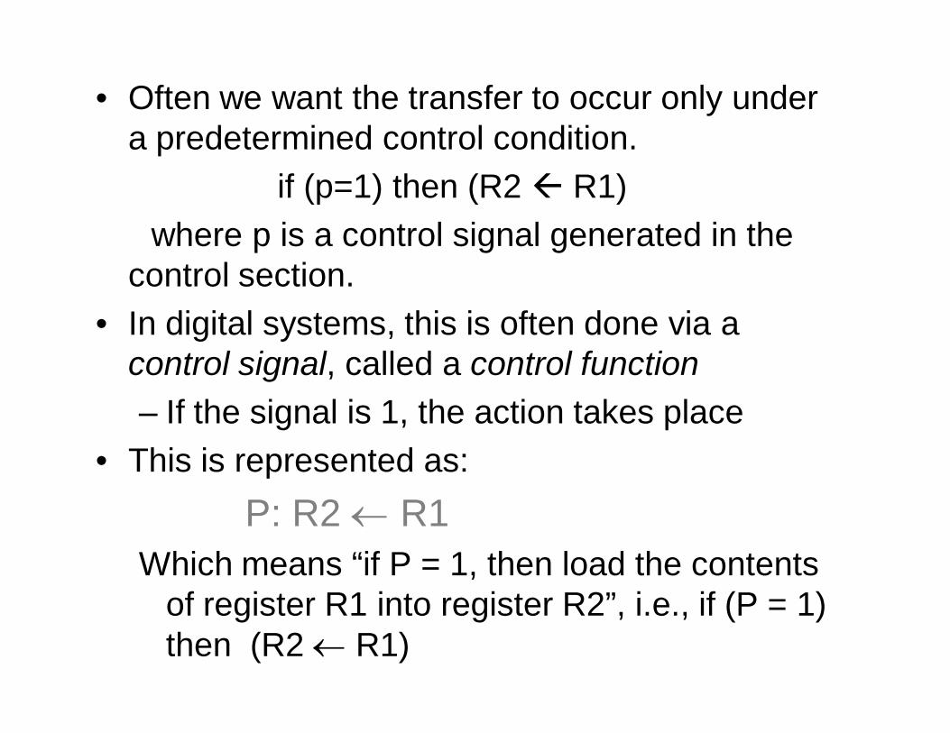
• Often we want the transfer to occur only under a predetermined control condition.
if (p=1) then (R2 R1)where p is a control signal generated in the
control section. • In digital systems, this is often done via a
control signal, called a control function– If the signal is 1, the action takes place
• This is represented as:P: R2 R1
Which means “if P = 1, then load the contents of register R1 into register R2”, i.e., if (P = 1) then (R2 R1)
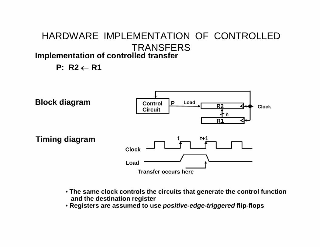
HARDWARE IMPLEMENTATION OF CONTROLLED TRANSFERS
Implementation of controlled transfer P: R2 R1
Block diagram
Timing diagram
Clock
Transfer occurs here
R2
R1
Control Circuit
LoadP
n
Clock
Load
t t+1
• The same clock controls the circuits that generate the control functionand the destination register
• Registers are assumed to use positive-edge-triggered flip-flops
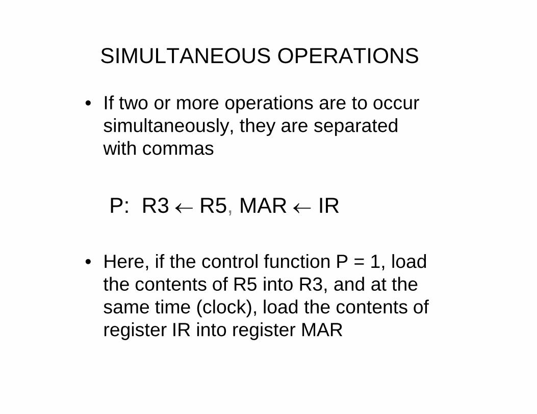
SIMULTANEOUS OPERATIONS
• If two or more operations are to occur simultaneously, they are separated with commas
P: R3 R5, MAR IR
• Here, if the control function P = 1, load the contents of R5 into R3, and at the same time (clock), load the contents of register IR into register MAR

BASIC SYMBOLS FOR REGISTER TRANSFERS
Capital letters Denotes a register MAR, R2& numerals
Parentheses () Denotes a part of a register R2(0-7), R2(L)
Arrow Denotes transfer of information R2 R1Colon : Denotes termination of control function P:Comma , Separates two micro-operations A B, B A
Symbols Description Examples
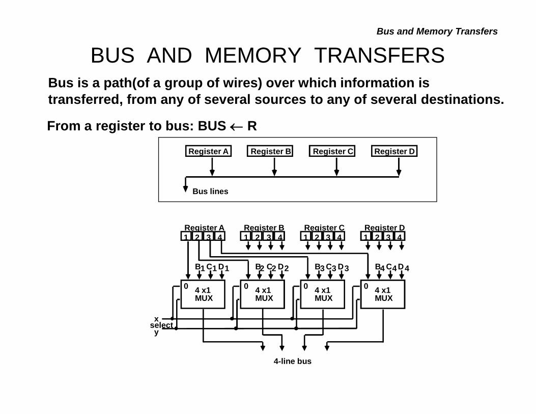
BUS AND MEMORY TRANSFERSBus is a path(of a group of wires) over which information is transferred, from any of several sources to any of several destinations.
From a register to bus: BUS R
1 2 3 4 1 2 3 4 1 2 3 4 1 2 3 4Register A Register B Register C Register D
B C D1 1 1
4 x1MUX
B C D2 2 2
4 x1MUX
B C D3 3 3
4 x1MUX
B C D4 4 4
4 x1MUX
4-line bus
xy
select
0 0 0 0
Register A Register B Register C Register D
Bus lines
Bus and Memory Transfers
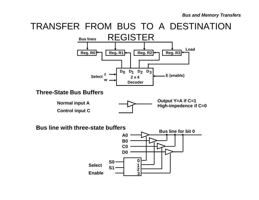
TRANSFER FROM BUS TO A DESTINATION REGISTER
Three-State Bus Buffers
Bus line with three-state buffers
Reg. R0 Reg. R1 Reg. R2 Reg. R3
Bus lines
2 x 4Decoder
Load
D0 D1 D2 D3zw
Select E (enable)
Output Y=A if C=1High-impedence if C=0Normal input A
Control input C
SelectEnable
0123
S0S1
A0B0C0D0
Bus line for bit 0
Bus and Memory Transfers
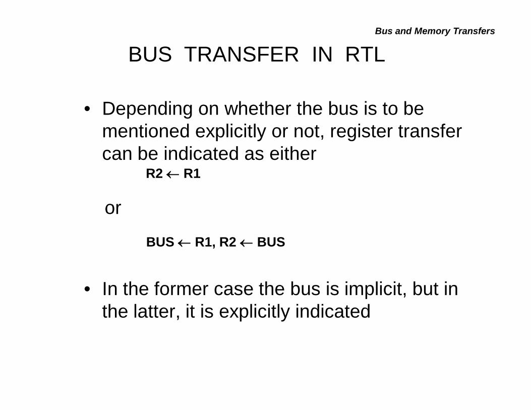
BUS TRANSFER IN RTLBus and Memory Transfers
• Depending on whether the bus is to be mentioned explicitly or not, register transfer can be indicated as either
or
• In the former case the bus is implicit, but in the latter, it is explicitly indicated
R2 R1
BUS R1, R2 BUS
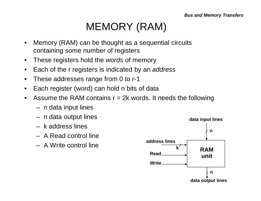
MEMORY (RAM)Bus and Memory Transfers
• Memory (RAM) can be thought as a sequential circuits containing some number of registers
• These registers hold the words of memory• Each of the r registers is indicated by an address• These addresses range from 0 to r-1• Each register (word) can hold n bits of data• Assume the RAM contains r = 2k words. It needs the following
– n data input lines– n data output lines– k address lines– A Read control line– A Write control line
data input lines
data output lines
n
n
kaddress lines
Read
Write
RAMunit
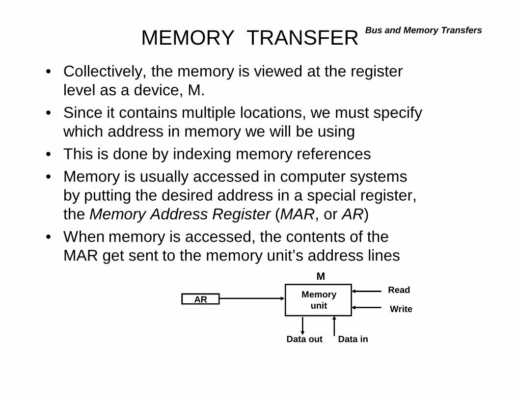
MEMORY TRANSFER Bus and Memory Transfers
• Collectively, the memory is viewed at the register level as a device, M.
• Since it contains multiple locations, we must specify which address in memory we will be using
• This is done by indexing memory references• Memory is usually accessed in computer systems
by putting the desired address in a special register, the Memory Address Register (MAR, or AR)
• When memory is accessed, the contents of the MAR get sent to the memory unit’s address lines
AR Memoryunit
Read
Write
Data inData out
M
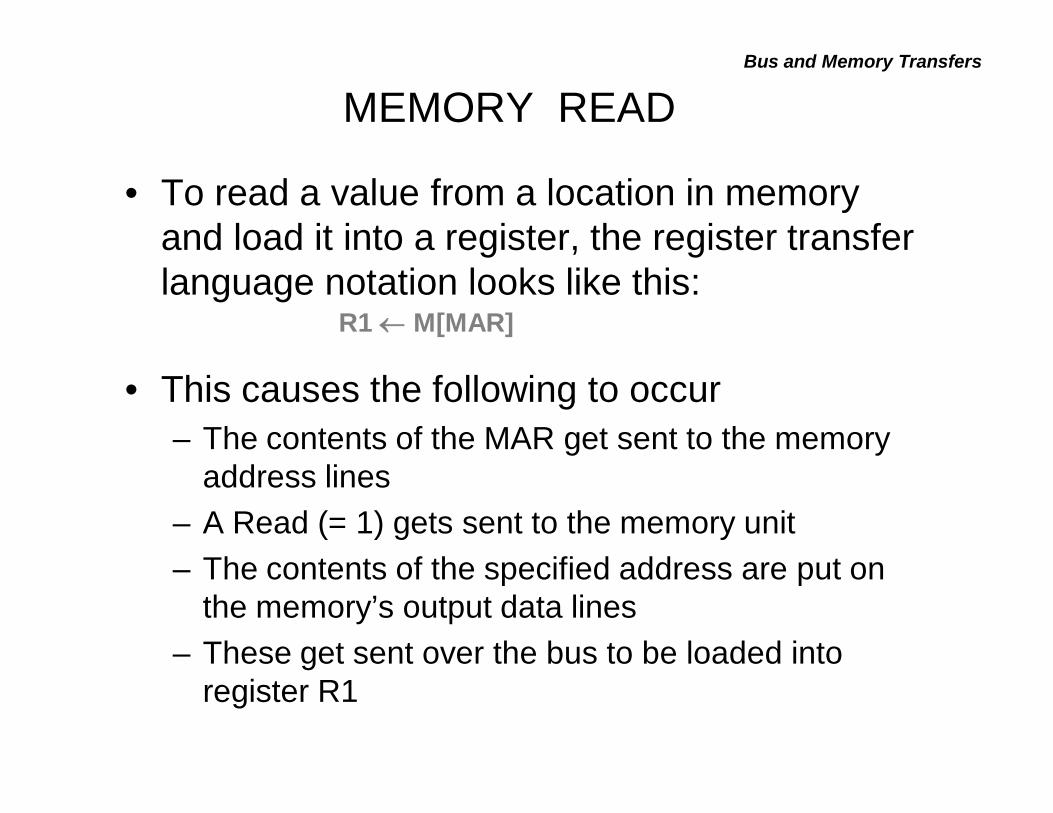
MEMORY READBus and Memory Transfers
• To read a value from a location in memory and load it into a register, the register transfer language notation looks like this:
• This causes the following to occur– The contents of the MAR get sent to the memory
address lines– A Read (= 1) gets sent to the memory unit– The contents of the specified address are put on
the memory’s output data lines– These get sent over the bus to be loaded into
register R1
R1 M[MAR]
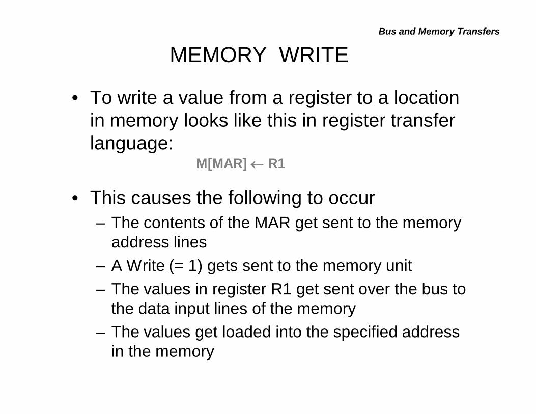
MEMORY WRITEBus and Memory Transfers
• To write a value from a register to a location in memory looks like this in register transfer language:
• This causes the following to occur– The contents of the MAR get sent to the memory
address lines– A Write (= 1) gets sent to the memory unit– The values in register R1 get sent over the bus to
the data input lines of the memory– The values get loaded into the specified address
in the memory
M[MAR] R1
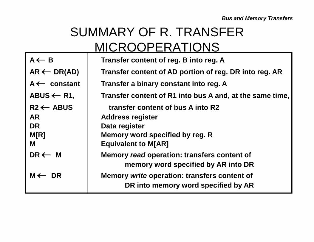
SUMMARY OF R. TRANSFER MICROOPERATIONS
Bus and Memory Transfers
A B Transfer content of reg. B into reg. AAR DR(AD) Transfer content of AD portion of reg. DR into reg. ARA constant Transfer a binary constant into reg. AABUS R1, Transfer content of R1 into bus A and, at the same time, R2 ABUS transfer content of bus A into R2 AR Address registerDR Data registerM[R] Memory word specified by reg. RM Equivalent to M[AR]DR M Memory read operation: transfers content of
memory word specified by AR into DRM DR Memory write operation: transfers content of
DR into memory word specified by AR
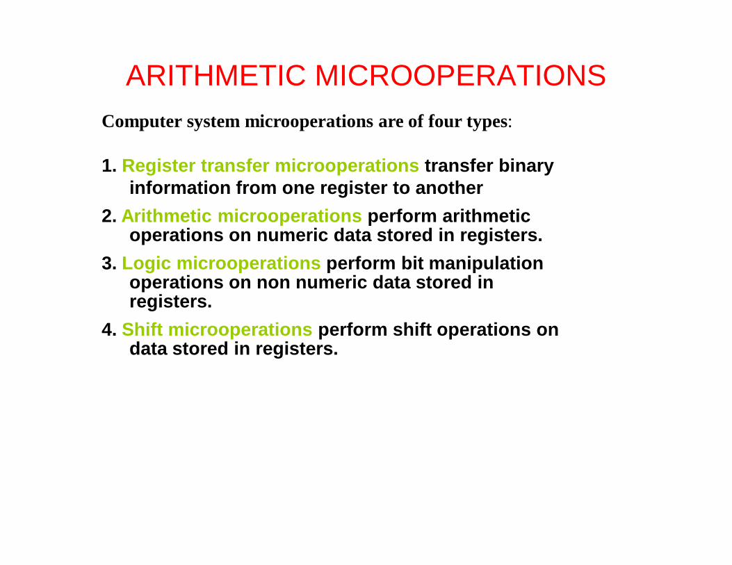
ARITHMETIC MICROOPERATIONSComputer system microoperations are of four types:
1. Register transfer microoperations transfer binary information from one register to another
2. Arithmetic microoperations perform arithmetic operations on numeric data stored in registers.
3. Logic microoperations perform bit manipulation operations on non numeric data stored in registers.
4. Shift microoperations perform shift operations on data stored in registers.
ARITHMETIC MICROOPERATIONS
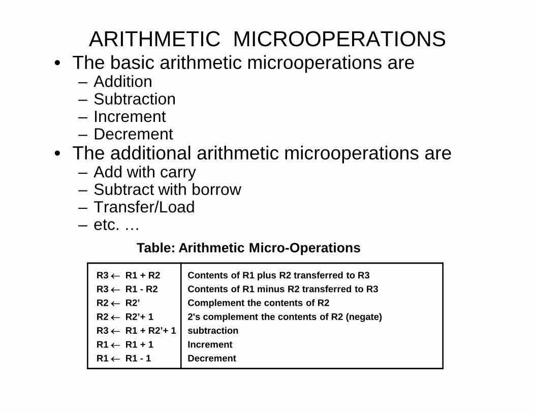
Table: Arithmetic Micro-Operations
R3 R1 + R2 Contents of R1 plus R2 transferred to R3R3 R1 - R2 Contents of R1 minus R2 transferred to R3R2 R2’ Complement the contents of R2 R2 R2’+ 1 2's complement the contents of R2 (negate)R3 R1 + R2’+ 1 subtractionR1 R1 + 1 IncrementR1 R1 - 1 Decrement
• The basic arithmetic microoperations are– Addition– Subtraction– Increment– Decrement
• The additional arithmetic microoperations are– Add with carry– Subtract with borrow– Transfer/Load– etc. …
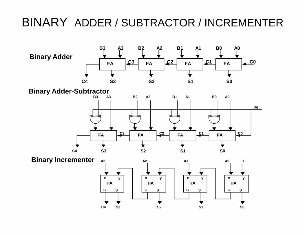
BINARY ADDER / SUBTRACTOR / INCREMENTER
FA
B0 A0
S0
C0FA
B1 A1
S1
C1FA
B2 A2
S2
C2FA
B3 A3
S3
C3
C4
Binary Adder-Subtractor
FA
B0 A0
S0
C0C1FA
B1 A1
S1
C2FA
B2 A2
S2
C3FA
B3 A3
S3C4
M
Binary Incrementer
HAx y
C S
A0 1
S0
HAx y
C S
A1
S1
HAx y
C S
A2
S2
HAx y
C S
A3
S3C4
Binary Adder

ARITHMETIC CIRCUIT
S1S00123
4x1MUX
X0
Y0
C0
C1D0FA
S1S00123
4x1MUX
X1
Y1
C1
C2D1FA
S1S00123
4x1MUX
X2
Y2
C2
C3D2FA
S1S00123
4x1MUX
X3
Y3
C3
C4D3FA
Cout
A0
B0
A1
B1
A2
B2
A3
B3
0 1
S0S1Cin
S1 S0 Cin Y Output Microoperation0 0 0 B D = A + B Add0 0 1 B D = A + B + 1 Add with carry0 1 0 B’ D = A + B’ Subtract with borrow0 1 1 B’ D = A + B’+ 1 Subtract1 0 0 0 D = A Transfer A 1 0 1 0 D = A + 1 Increment A1 1 0 1 D = A - 1 Decrement A1 1 1 1 D = A Transfer A
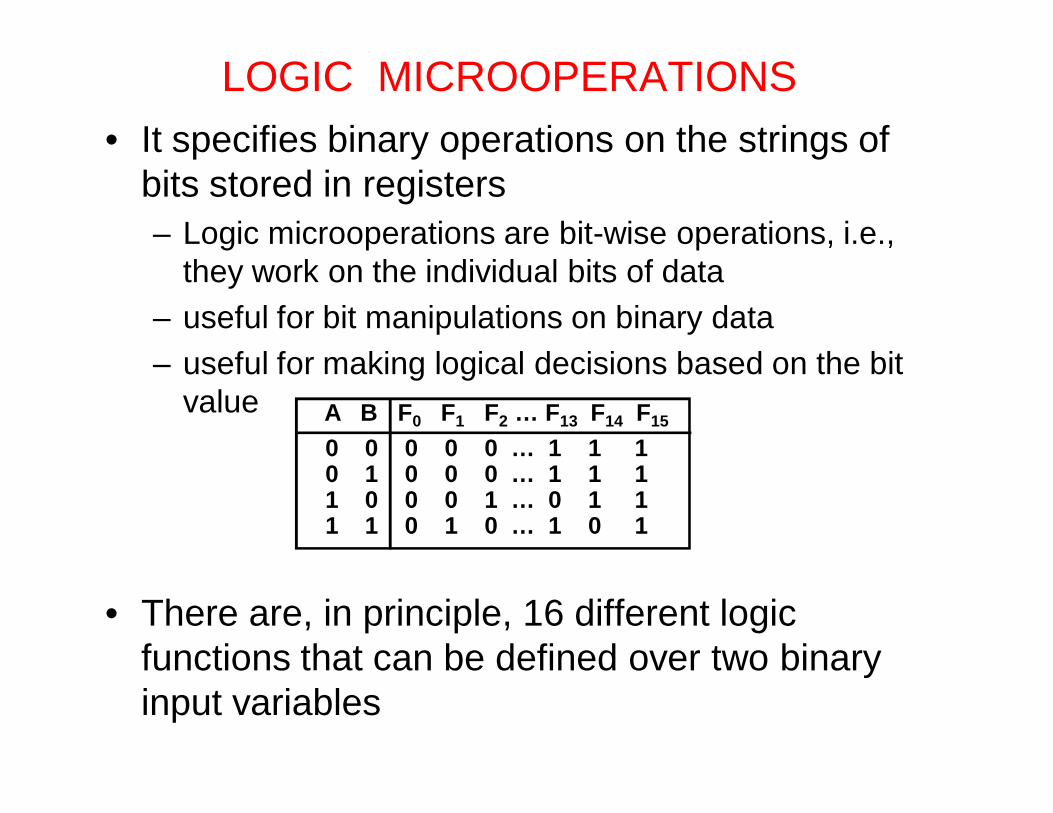
LOGIC MICROOPERATIONS• It specifies binary operations on the strings of
bits stored in registers– Logic microoperations are bit-wise operations, i.e.,
they work on the individual bits of data– useful for bit manipulations on binary data – useful for making logical decisions based on the bit
value
• There are, in principle, 16 different logic functions that can be defined over two binary input variables
0 0 0 0 0 … 1 1 10 1 0 0 0 … 1 1 11 0 0 0 1 … 0 1 11 1 0 1 0 … 1 0 1
A B F0 F1 F2 … F13 F14 F15

LIST OF LOGIC MICROOPERATIONS• List of Logic Microoperations
- 16 different logic operations with 2 binary vars.- n binary vars → functions2 2 n
• Truth tables for 16 functions of 2 variables and thecorresponding 16 logic micro-operations
BooleanFunction
Micro-Operations Namex 0 0 1 1
y 0 1 0 1
Logic Microoperations
0 0 0 0 F0 = 0 F 0 Clear0 0 0 1 F1 = xy F A B AND0 0 1 0 F2 = xy' F A B’0 0 1 1 F3 = x F A Transfer A0 1 0 0 F4 = x'y F A’ B0 1 0 1 F5 = y F B Transfer B0 1 1 0 F6 = x y F A B Exclusive-OR0 1 1 1 F7 = x + y F A B OR1 0 0 0 F8 = (x + y)' F A B)’ NOR1 0 0 1 F9 = (x y)' F (A B)’ Exclusive-NOR1 0 1 0 F10 = y' F B’ Complement B1 0 1 1 F11 = x + y' F A B1 1 0 0 F12 = x' F A’ Complement A1 1 0 1 F13 = x' + y F A’ B1 1 1 0 F14 = (xy)' F (A B)’ NAND1 1 1 1 F15 = 1 F all 1's Set to all 1's
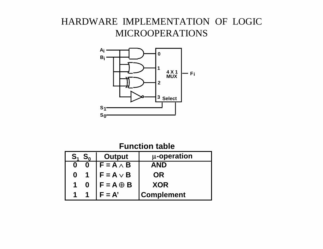
HARDWARE IMPLEMENTATION OF LOGIC MICROOPERATIONS
0 0 F = A B AND0 1 F = AB OR1 0 F = A B XOR1 1 F = A’ Complement
S1 S0 Output -operationFunction table
BA
SS
F
10
i
ii 0
1
2
3
4 X 1MUX
Select
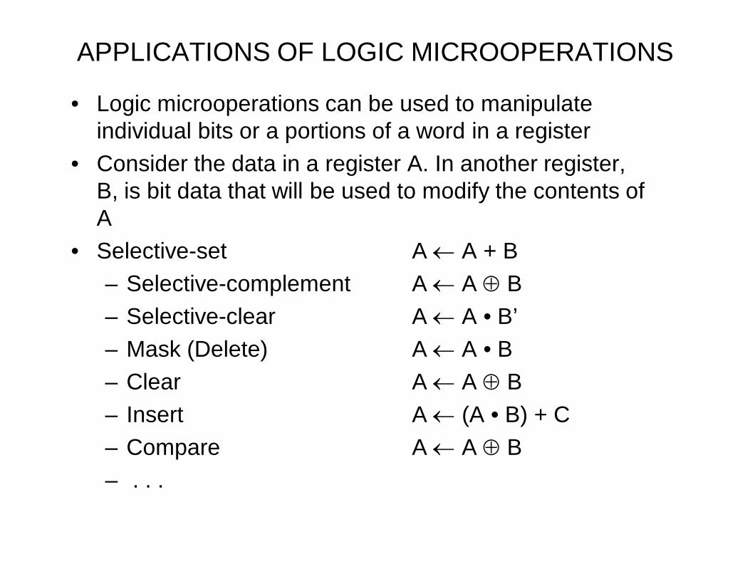
APPLICATIONS OF LOGIC MICROOPERATIONS
• Logic microoperations can be used to manipulate individual bits or a portions of a word in a register
• Consider the data in a register A. In another register, B, is bit data that will be used to modify the contents of A
• Selective-set A A + B– Selective-complement A A B– Selective-clear A A • B’– Mask (Delete) A A • B– Clear A A B– Insert A (A • B) + C– Compare A A B– . . .
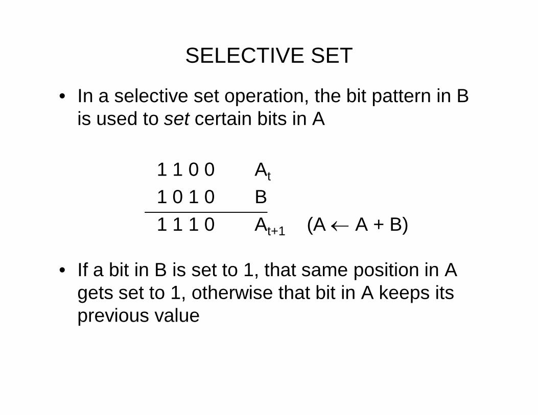
SELECTIVE SET
• In a selective set operation, the bit pattern in B is used to set certain bits in A
1 1 0 0 At
1 0 1 0 B1 1 1 0 At+1 (A A + B)
• If a bit in B is set to 1, that same position in A gets set to 1, otherwise that bit in A keeps its previous value
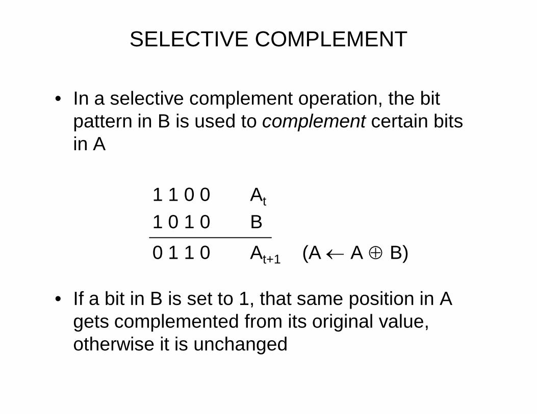
SELECTIVE COMPLEMENT
• In a selective complement operation, the bit pattern in B is used to complement certain bits in A
1 1 0 0 At
1 0 1 0 B0 1 1 0 At+1 (A A B)
• If a bit in B is set to 1, that same position in A gets complemented from its original value, otherwise it is unchanged
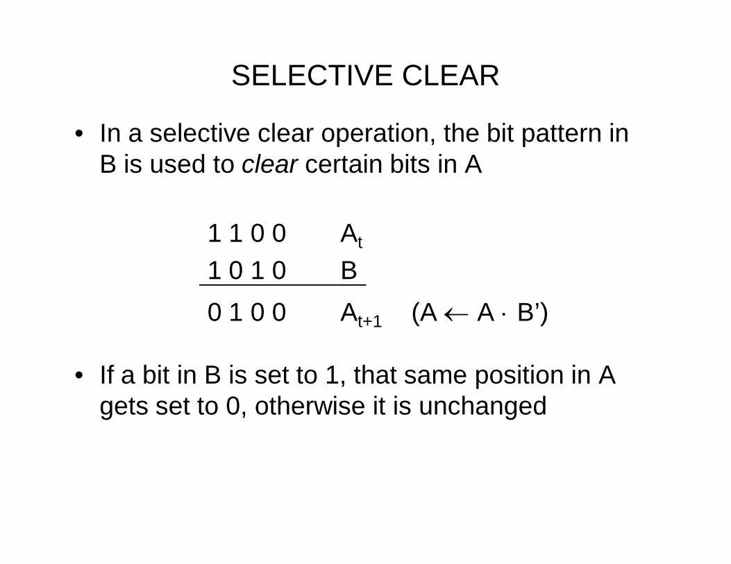
SELECTIVE CLEAR
• In a selective clear operation, the bit pattern in B is used to clear certain bits in A
1 1 0 0 At
1 0 1 0 B0 1 0 0 At+1 (A A B’)
• If a bit in B is set to 1, that same position in A gets set to 0, otherwise it is unchanged
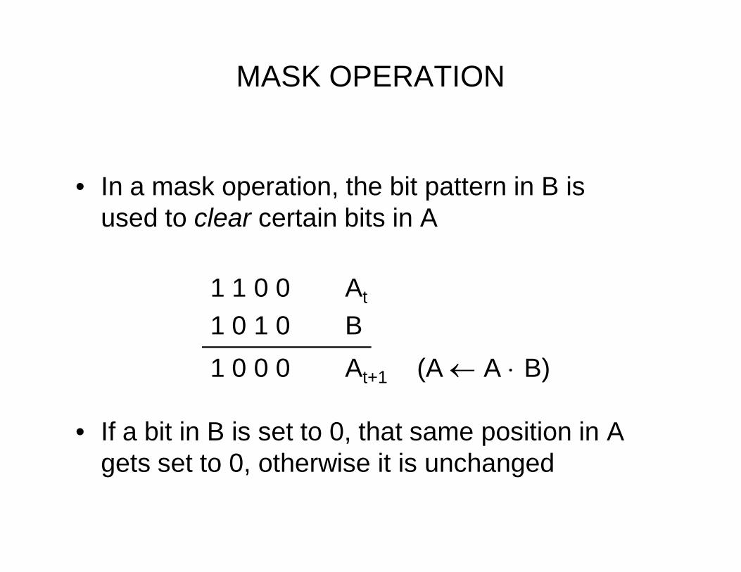
MASK OPERATION
• In a mask operation, the bit pattern in B is used to clear certain bits in A
1 1 0 0 At
1 0 1 0 B1 0 0 0 At+1 (A A B)
• If a bit in B is set to 0, that same position in A gets set to 0, otherwise it is unchanged
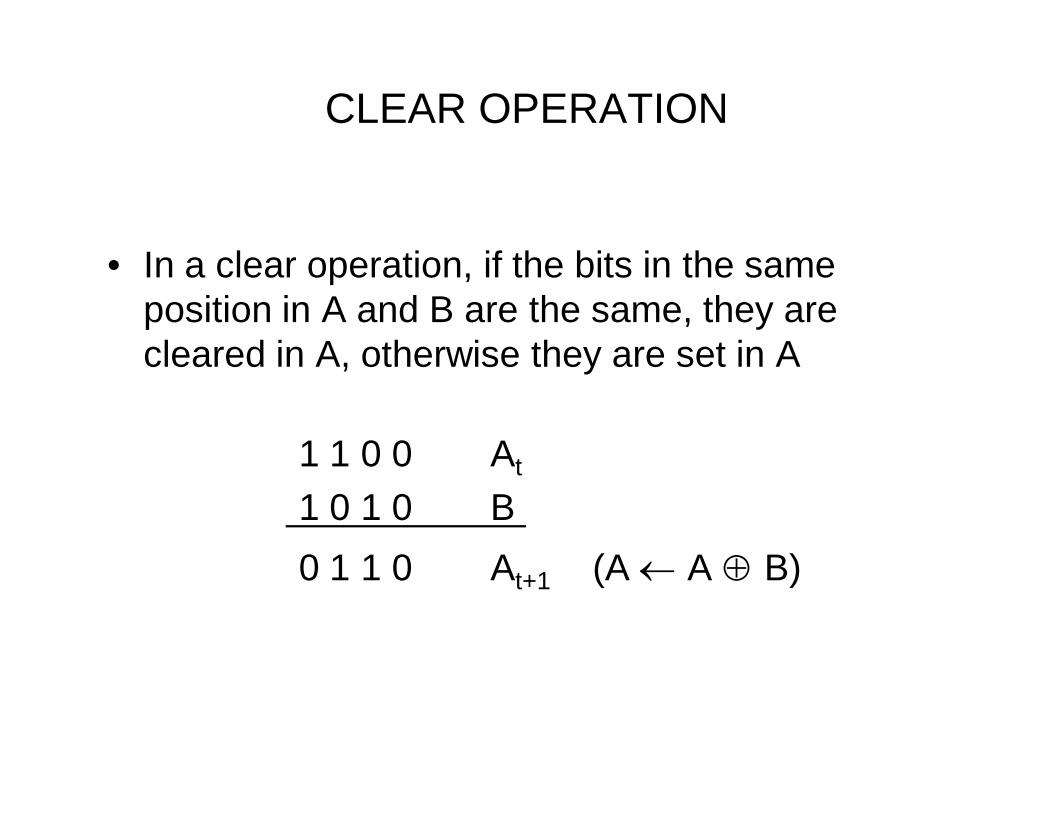
CLEAR OPERATION
• In a clear operation, if the bits in the same position in A and B are the same, they are cleared in A, otherwise they are set in A
1 1 0 0 At
1 0 1 0 B0 1 1 0 At+1 (A A B)
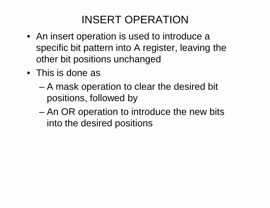
INSERT OPERATION• An insert operation is used to introduce a
specific bit pattern into A register, leaving the other bit positions unchanged
• This is done as– A mask operation to clear the desired bit
positions, followed by– An OR operation to introduce the new bits
into the desired positions

– Example• Suppose you wanted to introduce 1010 into the low order
four bits of A: 1101 1000 1011 0001 A (Original)1101 1000 1011 1010 A (Desired)
• 1101 1000 1011 0001 A (Original)1111 1111 1111 0000 Mask1101 1000 1011 0000 A (Intermediate)0000 0000 0000 1010 Added bits
1101 1000 1011 1010 A (Desired)
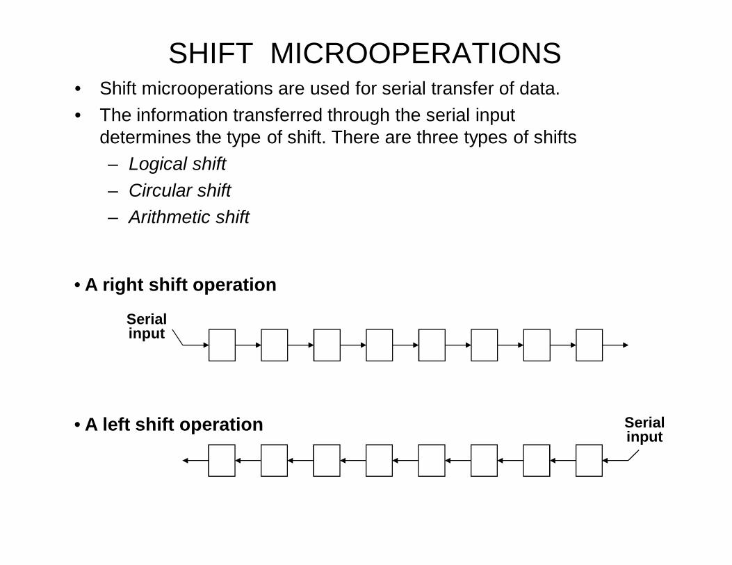
SHIFT MICROOPERATIONS• Shift microoperations are used for serial transfer of data.• The information transferred through the serial input
determines the type of shift. There are three types of shifts– Logical shift– Circular shift– Arithmetic shift
Serialinput
• A right shift operation
• A left shift operation Serialinput
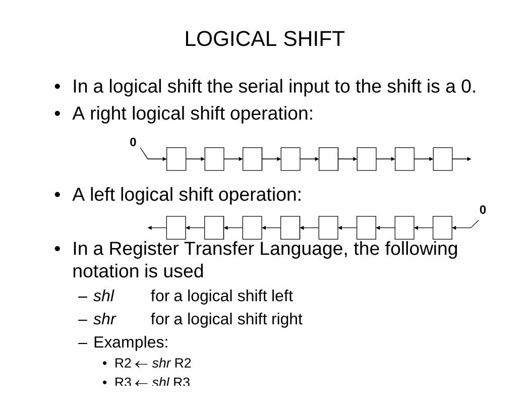
LOGICAL SHIFT
• In a logical shift the serial input to the shift is a 0.• A right logical shift operation:
• A left logical shift operation:
• In a Register Transfer Language, the following notation is used– shl for a logical shift left– shr for a logical shift right– Examples:
• R2 shr R2• R3 shl R3
0
0
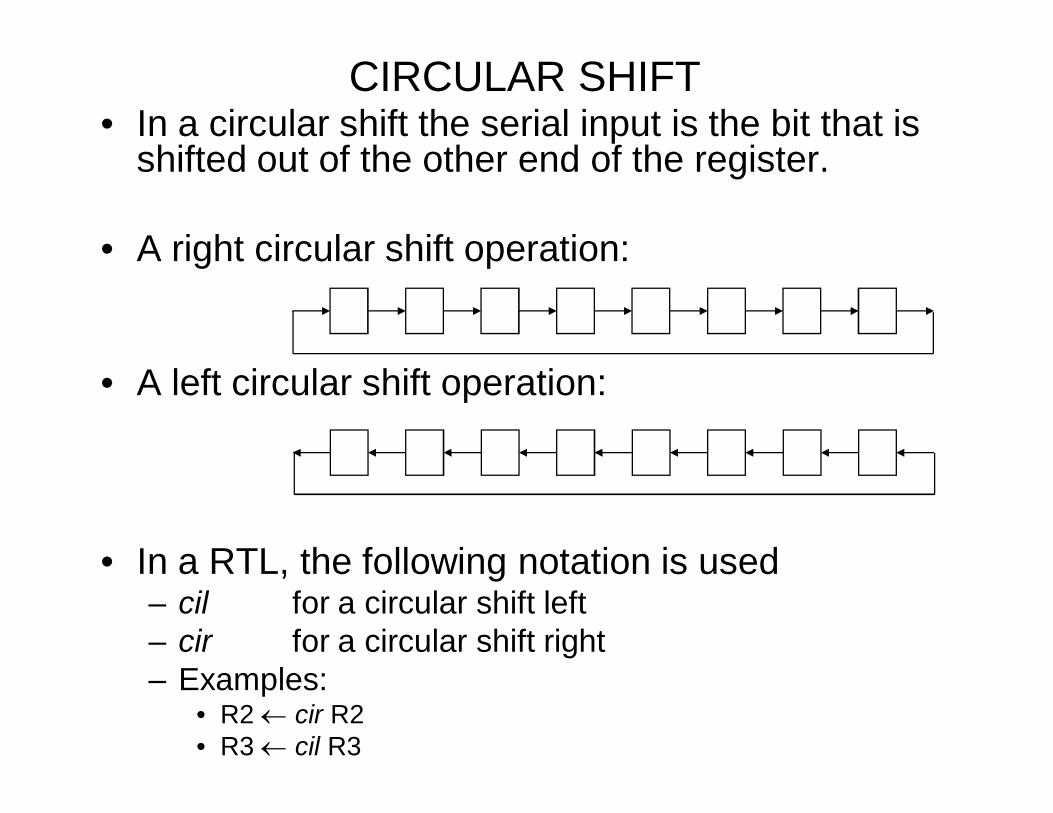
CIRCULAR SHIFT• In a circular shift the serial input is the bit that is
shifted out of the other end of the register.
• A right circular shift operation:
• A left circular shift operation:
• In a RTL, the following notation is used– cil for a circular shift left– cir for a circular shift right– Examples:
• R2 cir R2• R3 cil R3
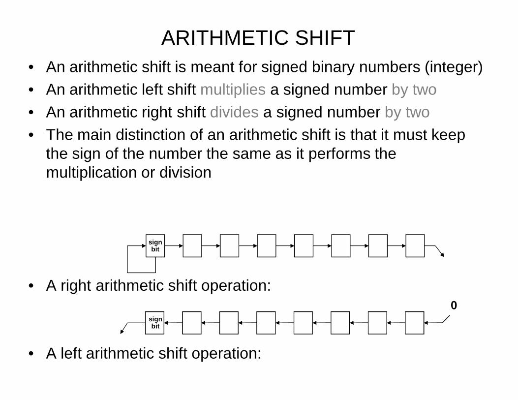
ARITHMETIC SHIFT• An arithmetic shift is meant for signed binary numbers (integer)• An arithmetic left shift multiplies a signed number by two• An arithmetic right shift divides a signed number by two• The main distinction of an arithmetic shift is that it must keep
the sign of the number the same as it performs the multiplication or division
• A right arithmetic shift operation:
• A left arithmetic shift operation:
0
signbit
signbit
ARITHMETIC SHIFT
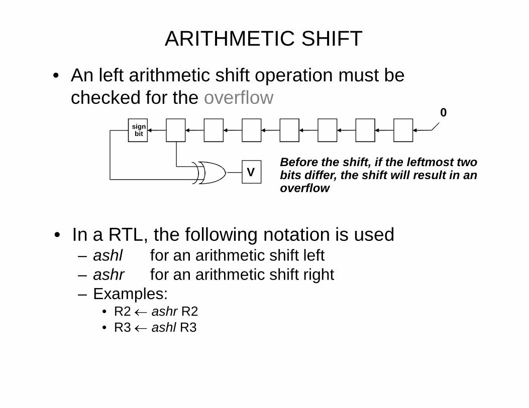
• An left arithmetic shift operation must be checked for the overflow
0
VBefore the shift, if the leftmost twobits differ, the shift will result in anoverflow
• In a RTL, the following notation is used– ashl for an arithmetic shift left– ashr for an arithmetic shift right– Examples:
• R2 ashr R2• R3 ashl R3
signbit
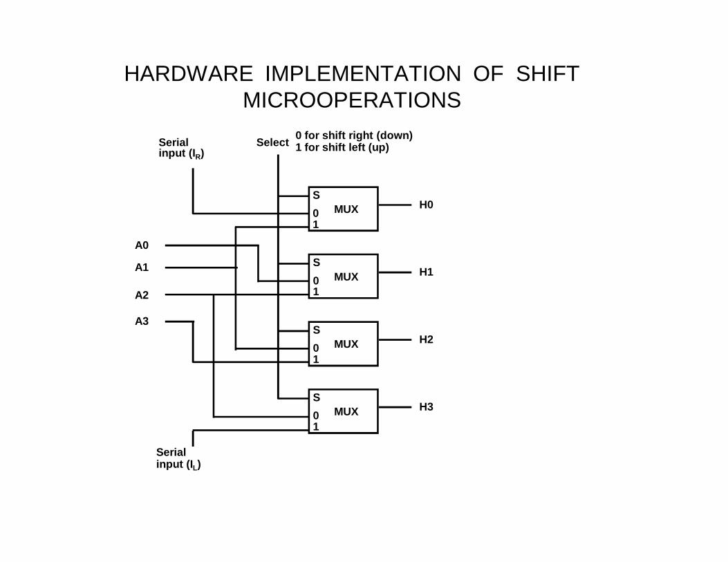
HARDWARE IMPLEMENTATION OF SHIFT MICROOPERATIONS
S01
H0MUX
S01
H1MUX
S01
H2MUX
S01
H3MUX
Select 0 for shift right (down) 1 for shift left (up)Serial
input (IR)
A0
A1
A2
A3
Serialinput (IL)
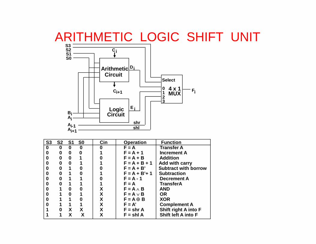
ARITHMETIC LOGIC SHIFT UNIT
S3 S2 S1 S0 Cin Operation Function0 0 0 0 0 F = A Transfer A0 0 0 0 1 F = A + 1 Increment A0 0 0 1 0 F = A + B Addition0 0 0 1 1 F = A + B + 1 Add with carry0 0 1 0 0 F = A + B’ Subtract with borrow0 0 1 0 1 F = A + B’+ 1 Subtraction0 0 1 1 0 F = A - 1 Decrement A0 0 1 1 1 F = A TransferA0 1 0 0 X F = A B AND0 1 0 1 X F = A B OR0 1 1 0 X F = A B XOR0 1 1 1 X F = A’ Complement A1 0 X X X F = shr A Shift right A into F1 1 X X X F = shl A Shift left A into F
ArithmeticCircuit
LogicCircuit
C
C 4 x 1MUX
Select
0123
F
S3S2S1S0
BA
i
A
D
A
E
shrshl
i+1 i
ii
i+1i-1
i
i

BASIC COMPUTER ORGANIZATION AND DESIGN• Instruction Codes
• Computer Registers
• Computer Instructions
• Timing and Control
• Instruction Cycle
• Memory Reference Instructions
• Input-Output and Interrupt
• Complete Computer Description
• Design of Basic Computer
• Design of Accumulator Logic
Instruction Codes• Every different processor type has its own design (different registers, buses,
microoperations, machine instructions, etc)• Modern processor is a very complex device• It contains
– Many registers– Multiple arithmetic units, for both integer and floating point calculations– The ability to pipeline several consecutive instructions to speed
execution– Etc.
• However, to understand how processors work, we will start with a simplified processor model
• This is similar to what real processors were like ~25 years ago• M. Morris Mano introduces a simple processor model he calls the Basic
Computer• We will use this to introduce processor organization and the relationship of
the RTL model to the higher level computer processor
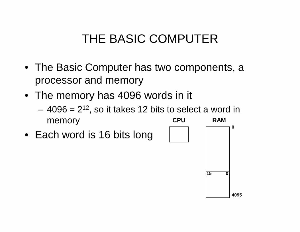
THE BASIC COMPUTER
• The Basic Computer has two components, a processor and memory
• The memory has 4096 words in it– 4096 = 212, so it takes 12 bits to select a word in
memory• Each word is 16 bits long
CPU RAM0
4095
015
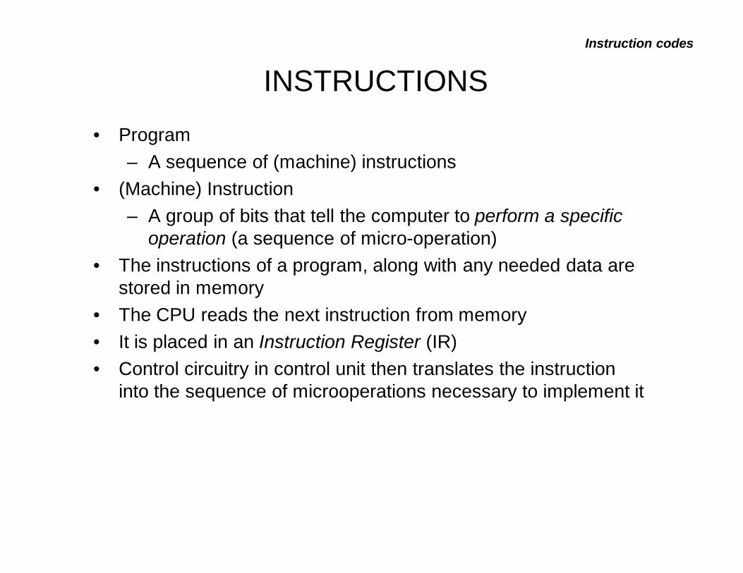
INSTRUCTIONSInstruction codes
• Program– A sequence of (machine) instructions
• (Machine) Instruction– A group of bits that tell the computer to perform a specific
operation (a sequence of micro-operation) • The instructions of a program, along with any needed data are
stored in memory• The CPU reads the next instruction from memory• It is placed in an Instruction Register (IR)• Control circuitry in control unit then translates the instruction
into the sequence of microoperations necessary to implement it
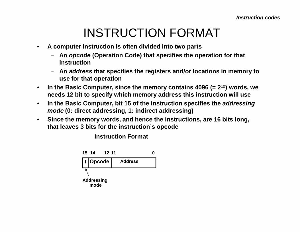
INSTRUCTION FORMATInstruction codes
• A computer instruction is often divided into two parts– An opcode (Operation Code) that specifies the operation for that
instruction– An address that specifies the registers and/or locations in memory to
use for that operation• In the Basic Computer, since the memory contains 4096 (= 212) words, we
needs 12 bit to specify which memory address this instruction will use • In the Basic Computer, bit 15 of the instruction specifies the addressing
mode (0: direct addressing, 1: indirect addressing)• Since the memory words, and hence the instructions, are 16 bits long,
that leaves 3 bits for the instruction’s opcode
Opcode Address
Instruction Format
15 14 12 0
I
11
Addressing mode
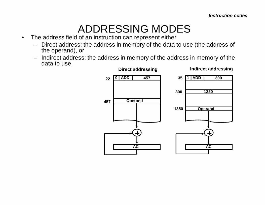
ADDRESSING MODESInstruction codes
• The address field of an instruction can represent either– Direct address: the address in memory of the data to use (the address of
the operand), or– Indirect address: the address in memory of the address in memory of the
data to use
0 ADD 45722
Operand457
1 ADD 30035
1350300
Operand1350
+AC
+AC
Direct addressing Indirect addressing
• Effective Address (EA)– The address, that can be directly used without
modification to access an operand for a computation-type instruction, or as the target address for a branch-type instruction
PROCESSOR REGISTERSInstruction codes
• A processor has many registers to hold instructions, addresses, data, etc• The processor has a register, the Program Counter (PC) that holds the
memory address of the next instruction to get– Since the memory in the Basic Computer only has 4096 locations, the
PC only needs 12 bits• In a direct or indirect addressing, the processor needs to keep track of
what locations in memory it is addressing: The Address Register (AR) is used for this– The AR is a 12 bit register in the Basic Computer
• When an operand is found, using either direct or indirect addressing, it is placed in the Data Register (DR). The processor then uses this value as data for its operation
• The Basic Computer has a single general purpose register – the Accumulator (AC)
PROCESSOR REGISTERSInstruction codes
• The significance of a general purpose register is that it can be referred to in instructions– e.g. load AC with the contents of a specific memory location; store the
contents of AC into a specified memory location• Often a processor will need a scratch register to store intermediate results or
other temporary data; in the Basic Computer this is the Temporary Register(TR)
• The Basic Computer uses a very simple model of input/output (I/O) operations– Input devices are considered to send 8 bits of character data to the
processor– The processor can send 8 bits of character data to output devices
• The Input Register (INPR) holds an 8 bit character gotten from an input device
• The Output Register (OUTR) holds an 8 bit character to be send to an output device
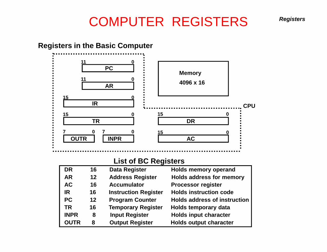
COMPUTER REGISTERS
List of BC RegistersDR 16 Data Register Holds memory operandAR 12 Address Register Holds address for memoryAC 16 Accumulator Processor registerIR 16 Instruction Register Holds instruction codePC 12 Program Counter Holds address of instructionTR 16 Temporary Register Holds temporary dataINPR 8 Input Register Holds input characterOUTR 8 Output Register Holds output character
Registers
Registers in the Basic Computer
11 0PC
15 0IR
15 0TR
7 0OUTR
15 0DR
15 0AC
11 0AR
INPR0 7
Memory4096 x 16
CPU
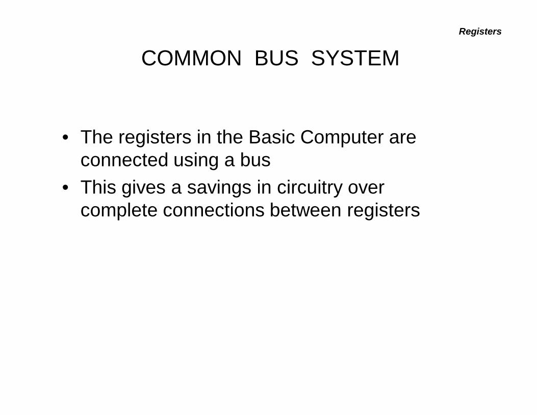
COMMON BUS SYSTEMRegisters
• The registers in the Basic Computer are connected using a bus
• This gives a savings in circuitry over complete connections between registers
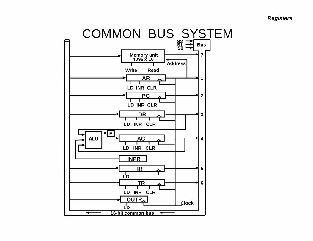
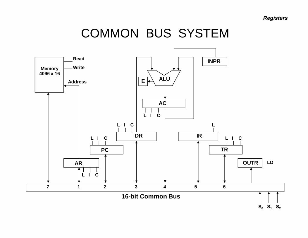
COMMON BUS SYSTEMRegisters
S2S1S0
Bus
Memory unit4096 x 16
LD INR CLR
AddressReadWrite
AR
LD INR CLR
PC
LD INR CLR
DR
LD INR CLR
ACALUE
INPR
IRLD
LD INR CLR
TR
OUTRLD
Clock
16-bit common bus
7
1
2
3
4
5
6
COMMON BUS SYSTEMRegisters
AR
PC
DR
L I C
L I C
L I C
AC
L I C
ALUE
IR
L
TR
L I C
OUTR LD
INPRMemory
4096 x 16
Address
Read
Write
16-bit Common Bus7 1 2 3 4 5 6
S0 S1 S2
COMMON BUS SYSTEMRegisters
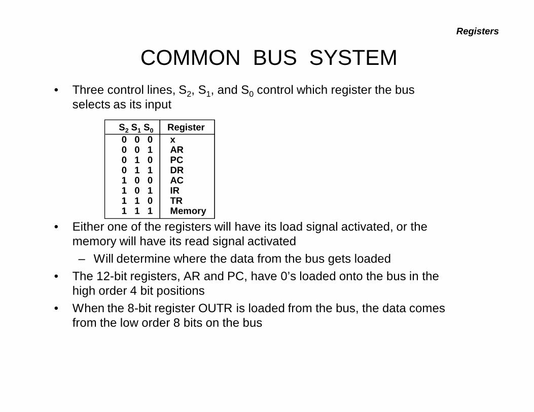
• Three control lines, S2, S1, and S0 control which register the bus selects as its input
• Either one of the registers will have its load signal activated, or the memory will have its read signal activated– Will determine where the data from the bus gets loaded
• The 12-bit registers, AR and PC, have 0’s loaded onto the bus in the high order 4 bit positions
• When the 8-bit register OUTR is loaded from the bus, the data comes from the low order 8 bits on the bus
0 0 0 x0 0 1 AR0 1 0 PC0 1 1 DR1 0 0 AC1 0 1 IR1 1 0 TR1 1 1 Memory
S2 S1 S0 Register
COMPUTER INSTRUCTIONSInstructions
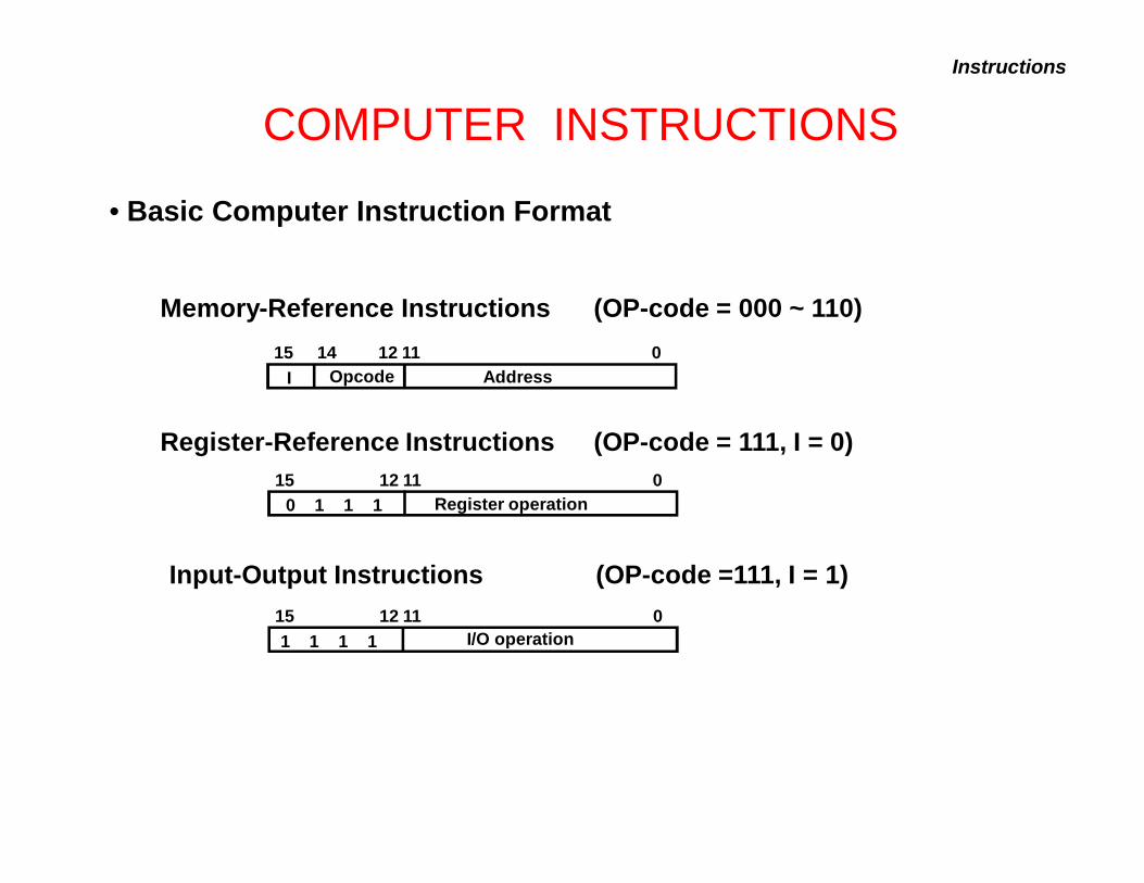
• Basic Computer Instruction Format
15 14 12 11 0I Opcode Address
Memory-Reference Instructions (OP-code = 000 ~ 110)
Register-Reference Instructions (OP-code = 111, I = 0)
Input-Output Instructions (OP-code =111, I = 1)
15 12 11 0Register operation0 1 1 1
15 12 11 0I/O operation1 1 1 1

BASIC COMPUTER INSTRUCTIONSHex Code
Symbol I = 0 I = 1 DescriptionAND 0xxx 8xxx AND memory word to ACADD 1xxx 9xxx Add memory word to ACLDA 2xxx Axxx Load AC from memorySTA 3xxx Bxxx Store content of AC into memoryBUN 4xxx Cxxx Branch unconditionallyBSA 5xxx Dxxx Branch and save return addressISZ 6xxx Exxx Increment and skip if zero
CLA 7800 Clear ACCLE 7400 Clear ECMA 7200 Complement ACCME 7100 Complement ECIR 7080 Circulate right AC and ECIL 7040 Circulate left AC and EINC 7020 Increment ACSPA 7010 Skip next instr. if AC is positiveSNA 7008 Skip next instr. if AC is negativeSZA 7004 Skip next instr. if AC is zeroSZE 7002 Skip next instr. if E is zeroHLT 7001 Halt computer
INP F800 Input character to ACOUT F400 Output character from ACSKI F200 Skip on input flagSKO F100 Skip on output flagION F080 Interrupt onIOF F040 Interrupt off
Instructions
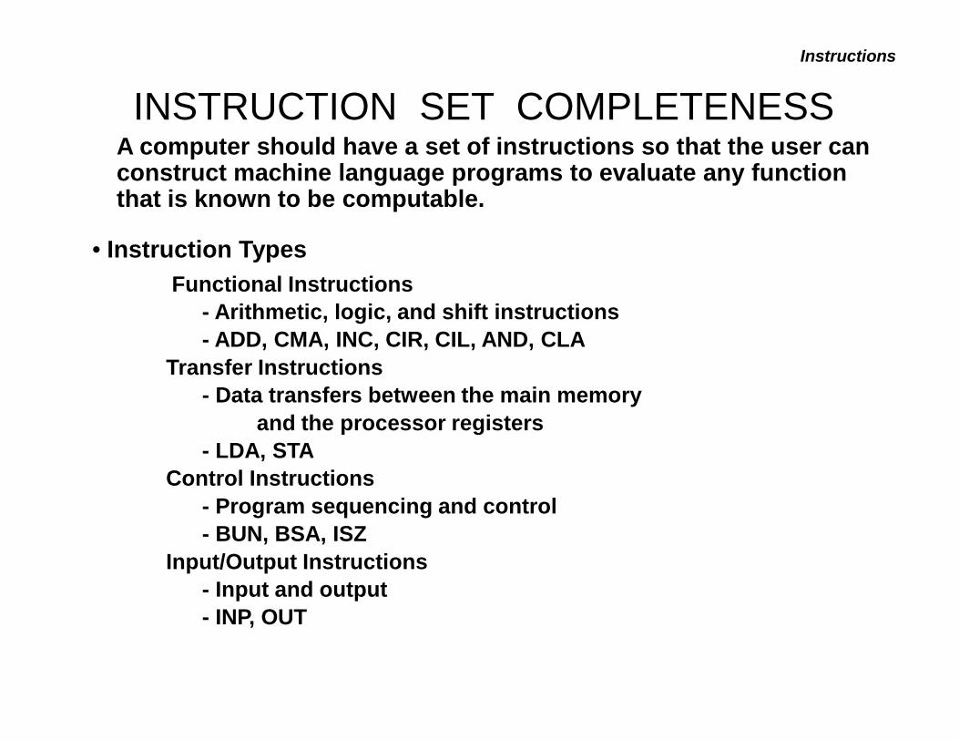
INSTRUCTION SET COMPLETENESS
• Instruction Types
A computer should have a set of instructions so that the user can construct machine language programs to evaluate any function that is known to be computable.
Functional Instructions- Arithmetic, logic, and shift instructions- ADD, CMA, INC, CIR, CIL, AND, CLA
Transfer Instructions- Data transfers between the main memory
and the processor registers- LDA, STA
Control Instructions- Program sequencing and control- BUN, BSA, ISZ
Input/Output Instructions- Input and output- INP, OUT
Instructions
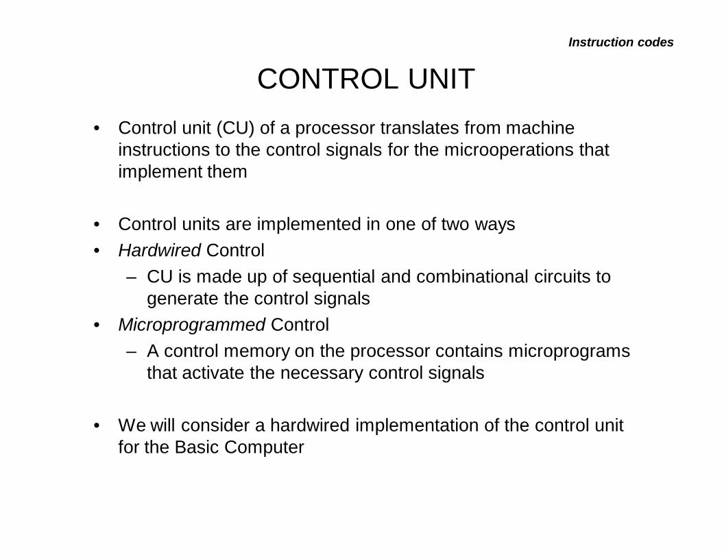
CONTROL UNITInstruction codes
• Control unit (CU) of a processor translates from machine instructions to the control signals for the microoperations that implement them
• Control units are implemented in one of two ways• Hardwired Control
– CU is made up of sequential and combinational circuits to generate the control signals
• Microprogrammed Control– A control memory on the processor contains microprograms
that activate the necessary control signals
• We will consider a hardwired implementation of the control unit for the Basic Computer
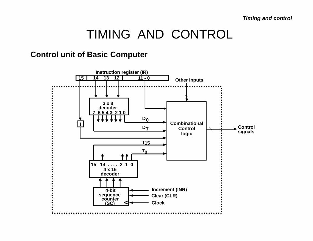
TIMING AND CONTROLControl unit of Basic Computer
Timing and control
Instruction register (IR)15 14 13 12 11 - 0
3 x 8decoder
7 6 5 4 3 2 1 0
ID0
15 14 . . . . 2 1 04 x 16
decoder
4-bitsequence
counter(SC)
Increment (INR)Clear (CLR)Clock
Other inputs
Controlsignals
D
T
T
7
15
0
CombinationalControl
logic

TIMING SIGNALS
ClockT0 T1 T2 T3 T4 T0
T0
T1
T2
T3
T4
D3
CLR SC
- Generated by 4-bit sequence counter and 416 decoder- The SC can be incremented or cleared.
- Example: T0, T1, T2, T3, T4, T0, T1, . . .Assume: At time T4, SC is cleared to 0 if decoder output D3 is active.
D3T4: SC 0
Timing and control
Fetch-Decode-Execute cycle (typically 3 to 5 stage)
INSTRUCTION CYCLE• In Basic Computer, a machine instruction is executed in the
following cycle:1. Fetch an instruction from memory2. Decode the instruction3. Read the effective address from memory if the instruction has
an indirect address4. Execute the instruction
• After an instruction is executed, the cycle starts again at step 1, for the next instruction
• Note: Every different processor has its own (different) instruction cycle
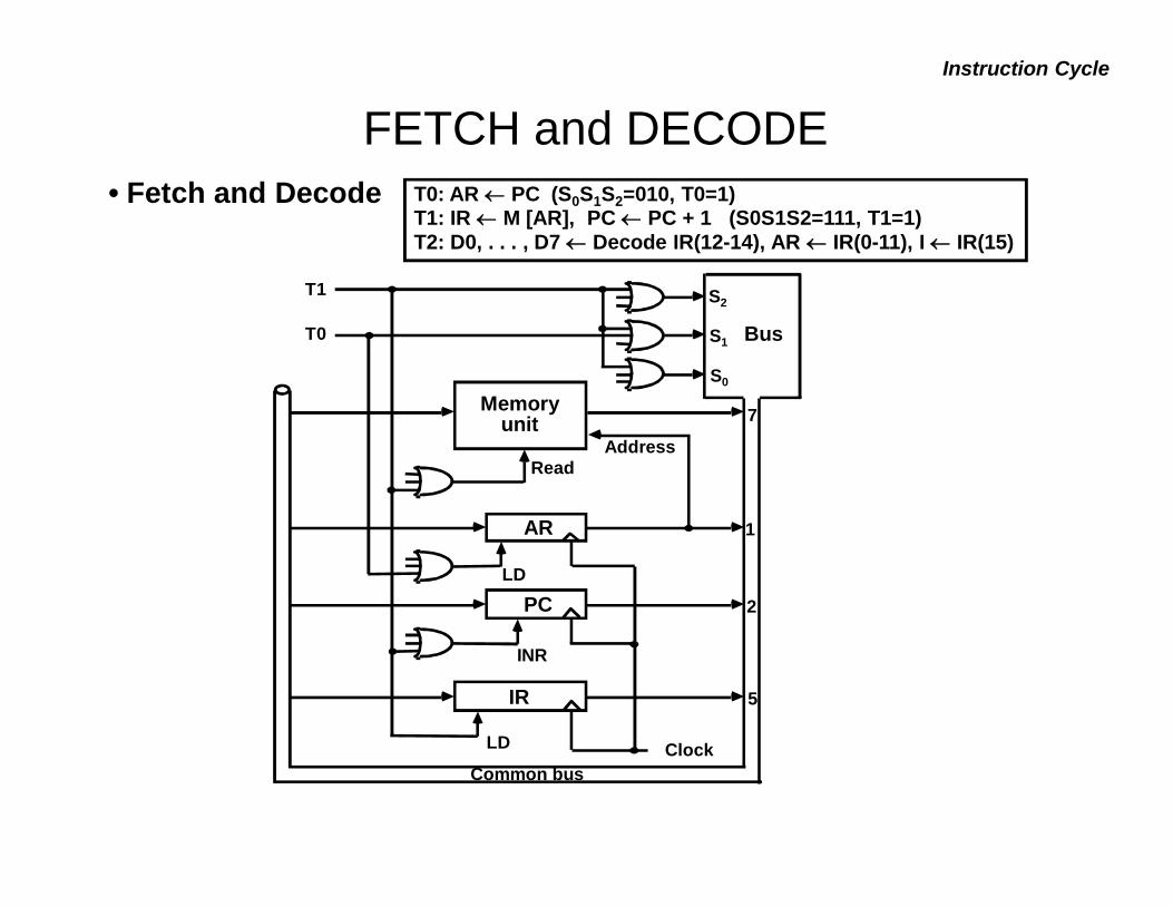
FETCH and DECODE• Fetch and Decode T0: AR PC (S0S1S2=010, T0=1)
T1: IR M [AR], PC PC + 1 (S0S1S2=111, T1=1)T2: D0, . . . , D7 Decode IR(12-14), AR IR(0-11), I IR(15)
S2
S1
S0
Bus
7Memoryunit
AddressRead
AR
LD
PC
INR
IR
LD Clock
1
2
5
Common bus
T1
T0
Instruction Cycle
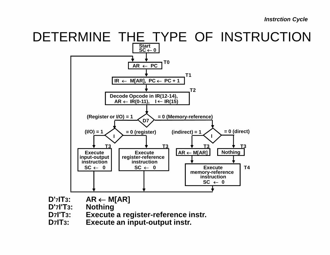
DETERMINE THE TYPE OF INSTRUCTION
= 0 (direct)
D'7IT3: AR M[AR]D'7I'T3: NothingD7I'T3: Execute a register-reference instr.D7IT3: Execute an input-output instr.
Instrction Cycle
StartSC 0
AR PCT0
IR M[AR], PC PC + 1T1
AR IR(0-11), I IR(15)Decode Opcode in IR(12-14),
T2
D7= 0 (Memory-reference)(Register or I/O) = 1
II
Executeregister-reference
instructionSC 0
Executeinput-outputinstruction
SC 0
M[AR]AR Nothing
= 0 (register)(I/O) = 1 (indirect) = 1
T3 T3 T3 T3
Executememory-reference
instructionSC 0
T4
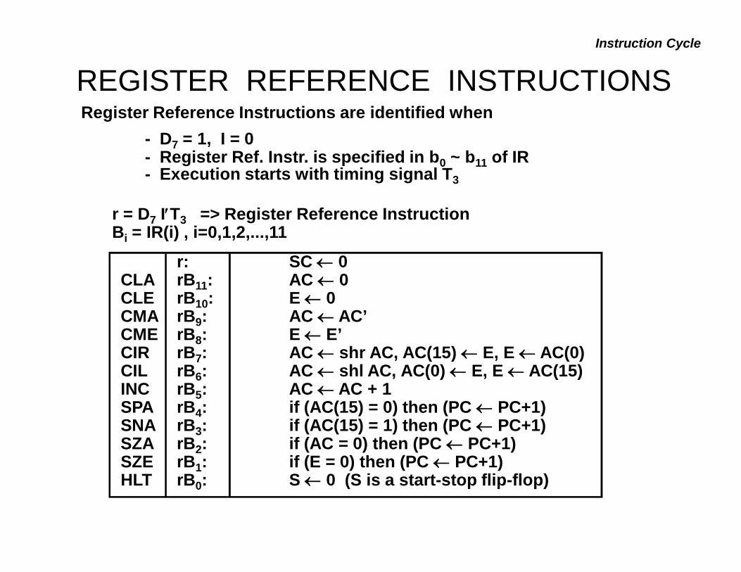
REGISTER REFERENCE INSTRUCTIONS
r = D7 IT3 => Register Reference InstructionBi = IR(i) , i=0,1,2,...,11
- D7 = 1, I = 0- Register Ref. Instr. is specified in b0 ~ b11 of IR- Execution starts with timing signal T3
Instruction Cycle
Register Reference Instructions are identified when
r: SC 0CLA rB11: AC 0CLE rB10: E 0CMA rB9: AC AC’CME rB8: E E’CIR rB7: AC shr AC, AC(15) E, E AC(0)CIL rB6: AC shl AC, AC(0) E, E AC(15)INC rB5: AC AC + 1SPA rB4: if (AC(15) = 0) then (PC PC+1)SNA rB3: if (AC(15) = 1) then (PC PC+1)SZA rB2: if (AC = 0) then (PC PC+1)SZE rB1: if (E = 0) then (PC PC+1)HLT rB0: S 0 (S is a start-stop flip-flop)
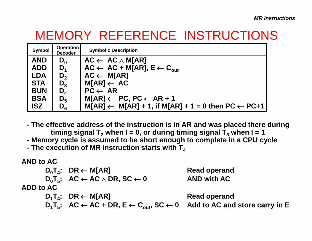
MEMORY REFERENCE INSTRUCTIONS
AND to ACD0T4: DR M[AR] Read operandD0T5: AC AC DR, SC 0 AND with AC
ADD to ACD1T4: DR M[AR] Read operandD1T5: AC AC + DR, E Cout, SC 0 Add to AC and store carry in E
- The effective address of the instruction is in AR and was placed there during timing signal T2 when I = 0, or during timing signal T3 when I = 1
- Memory cycle is assumed to be short enough to complete in a CPU cycle- The execution of MR instruction starts with T4
MR Instructions
Symbol OperationDecoder Symbolic Description
AND D0 AC AC M[AR]ADD D1 AC AC + M[AR], E CoutLDA D2 AC M[AR]STA D3 M[AR] ACBUN D4 PC ARBSA D5 M[AR] PC, PC AR + 1ISZ D6 M[AR] M[AR] + 1, if M[AR] + 1 = 0 then PC PC+1
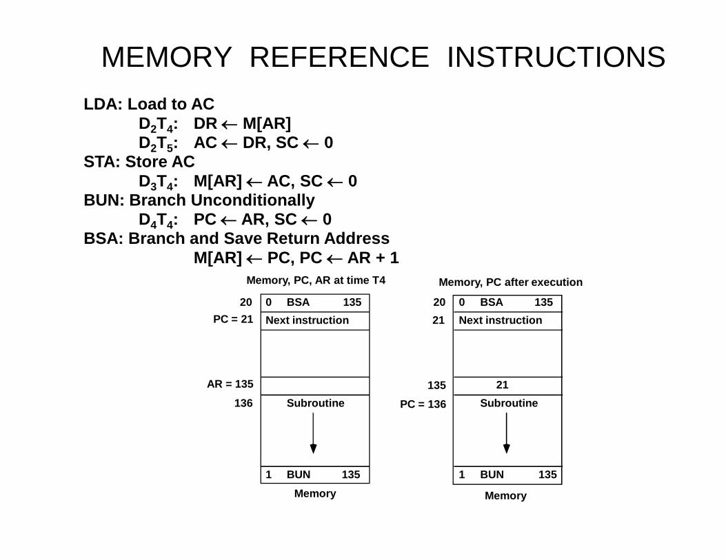
MEMORY REFERENCE INSTRUCTIONS
Memory, PC after execution
21
0 BSA 135Next instruction
Subroutine
20PC = 21
AR = 135
136
1 BUN 135
Memory, PC, AR at time T4
0 BSA 135Next instruction
Subroutine
2021
135PC = 136
1 BUN 135Memory Memory
LDA: Load to ACD2T4: DR M[AR]D2T5: AC DR, SC 0
STA: Store ACD3T4: M[AR] AC, SC 0
BUN: Branch UnconditionallyD4T4: PC AR, SC 0
BSA: Branch and Save Return AddressM[AR] PC, PC AR + 1
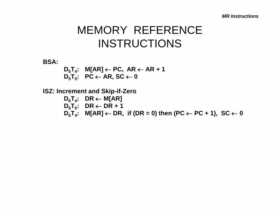
MEMORY REFERENCE INSTRUCTIONS
MR Instructions
BSA: D5T4: M[AR] PC, AR AR + 1D5T5: PC AR, SC 0
ISZ: Increment and Skip-if-ZeroD6T4: DR M[AR]D6T5: DR DR + 1D6T4: M[AR] DR, if (DR = 0) then (PC PC + 1), SC 0
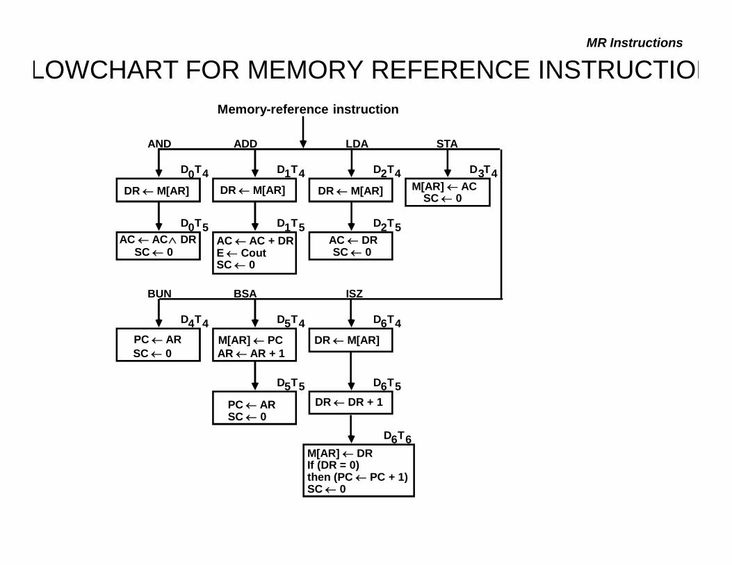
FLOWCHART FOR MEMORY REFERENCE INSTRUCTIONSMR Instructions
Memory-reference instruction
DR M[AR] DR M[AR] DR M[AR] M[AR] ACSC 0
AND ADD LDA STA
AC AC DRSC 0
AC AC + DRE CoutSC 0
AC DRSC 0
D T0 4 D T1 4 D T2 4 D T3 4
D T0 5 D T1 5 D T2 5
PC ARSC 0
M[AR] PCAR AR + 1
DR M[AR]
BUN BSA ISZ
D T4 4 D T5 4 D T6 4
DR DR + 1
D T5 5 D T6 5PC ARSC 0
M[AR] DRIf (DR = 0)then (PC PC + 1)SC 0
D T6 6
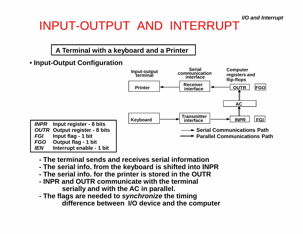
INPUT-OUTPUT AND INTERRUPT
• Input-Output Configuration
INPR Input register - 8 bitsOUTR Output register - 8 bitsFGI Input flag - 1 bitFGO Output flag - 1 bitIEN Interrupt enable - 1 bit
- The terminal sends and receives serial information- The serial info. from the keyboard is shifted into INPR - The serial info. for the printer is stored in the OUTR- INPR and OUTR communicate with the terminal
serially and with the AC in parallel.- The flags are needed to synchronize the timing
difference between I/O device and the computer
A Terminal with a keyboard and a Printer
I/O and Interrupt
Input-outputterminal
Serialcommunication
interfaceComputerregisters andflip-flops
Printer
Keyboard
Receiverinterface
Transmitterinterface
FGOOUTR
AC
INPR FGI
Serial Communications PathParallel Communications Path
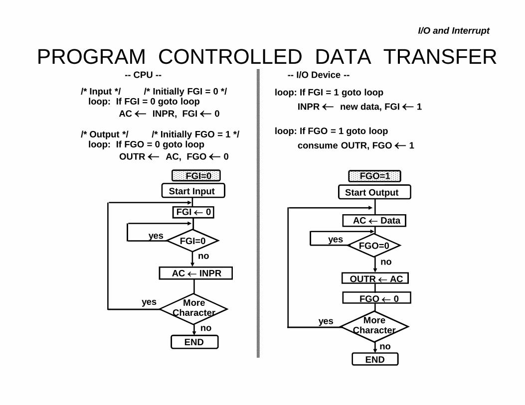
PROGRAM CONTROLLED DATA TRANSFERloop: If FGI = 1 goto loop
INPR new data, FGI 1
loop: If FGO = 1 goto loopconsume OUTR, FGO 1
-- CPU -- -- I/O Device --
/* Input */ /* Initially FGI = 0 */loop: If FGI = 0 goto loop
AC INPR, FGI 0
/* Output */ /* Initially FGO = 1 */loop: If FGO = 0 goto loop
OUTR AC, FGO 0
I/O and Interrupt
Start Input
FGI 0
FGI=0
AC INPR
MoreCharacter
END
Start Output
FGO 0
FGO=0
MoreCharacter
END
OUTR AC
AC Datayes
no
yes
no
FGI=0 FGO=1
yes
yesno
no
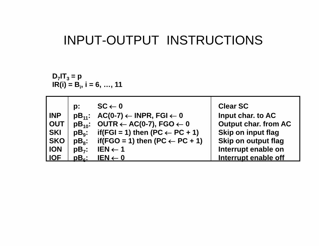
INPUT-OUTPUT INSTRUCTIONS
D7IT3 = pIR(i) = Bi, i = 6, …, 11
p: SC 0 Clear SCINP pB11: AC(0-7) INPR, FGI 0 Input char. to ACOUT pB10: OUTR AC(0-7), FGO 0 Output char. from ACSKI pB9: if(FGI = 1) then (PC PC + 1) Skip on input flagSKO pB8: if(FGO = 1) then (PC PC + 1) Skip on output flagION pB7: IEN 1 Interrupt enable onIOF pB6: IEN 0 Interrupt enable off
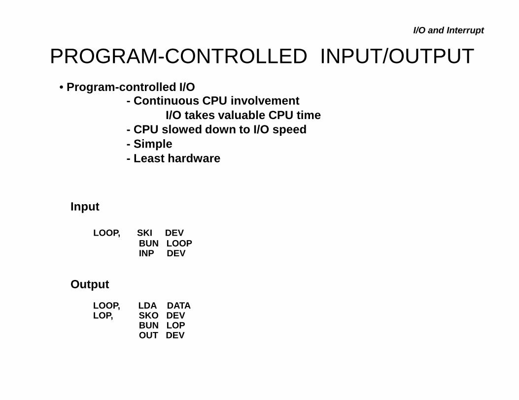
PROGRAM-CONTROLLED INPUT/OUTPUT• Program-controlled I/O
- Continuous CPU involvementI/O takes valuable CPU time
- CPU slowed down to I/O speed- Simple- Least hardware
I/O and Interrupt
Input
LOOP, SKI DEVBUN LOOPINP DEV
Output
LOOP, LDA DATALOP, SKO DEV
BUN LOPOUT DEV
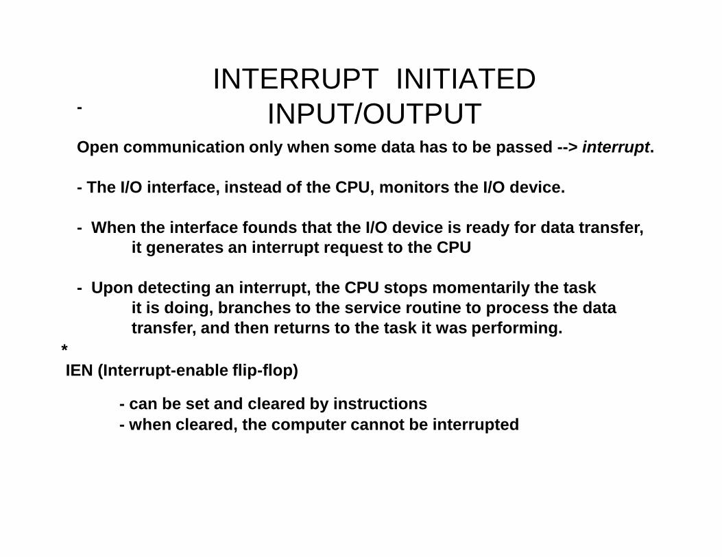
INTERRUPT INITIATED INPUT/OUTPUT-
Open communication only when some data has to be passed --> interrupt.
- The I/O interface, instead of the CPU, monitors the I/O device.
- When the interface founds that the I/O device is ready for data transfer, it generates an interrupt request to the CPU
- Upon detecting an interrupt, the CPU stops momentarily the task it is doing, branches to the service routine to process the data transfer, and then returns to the task it was performing.
*IEN (Interrupt-enable flip-flop)
- can be set and cleared by instructions- when cleared, the computer cannot be interrupted
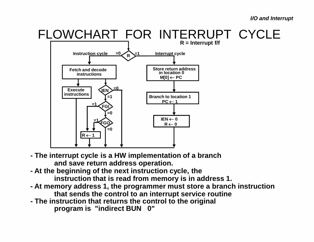
FLOWCHART FOR INTERRUPT CYCLER = Interrupt f/f
- The interrupt cycle is a HW implementation of a branchand save return address operation.
- At the beginning of the next instruction cycle, the instruction that is read from memory is in address 1.
- At memory address 1, the programmer must store a branch instruction that sends the control to an interrupt service routine
- The instruction that returns the control to the original program is "indirect BUN 0"
I/O and Interrupt
Store return address
R =1=0
in location 0M[0] PC
Branch to location 1PC 1
IEN 0R 0
Interrupt cycleInstruction cycle
Fetch and decodeinstructions
IEN
FGI
FGO
Executeinstructions
R 1
=1=1
=1
=0
=0
=0
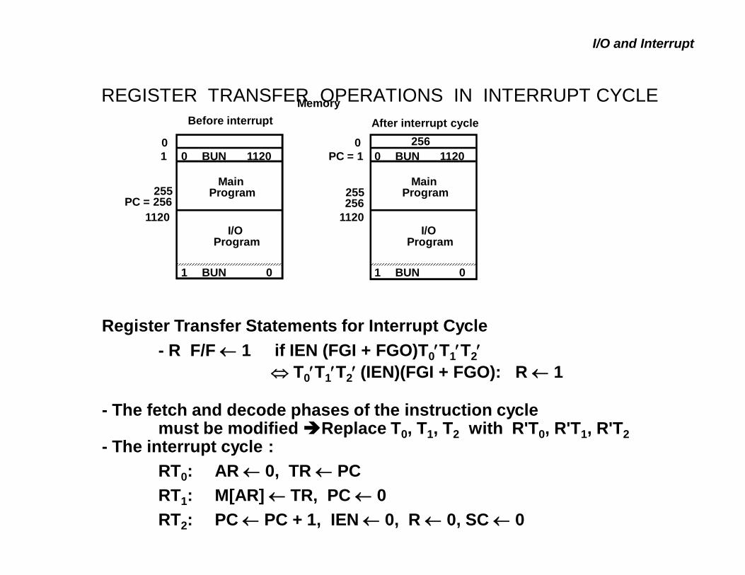
REGISTER TRANSFER OPERATIONS IN INTERRUPT CYCLE
Register Transfer Statements for Interrupt Cycle- R F/F 1 if IEN (FGI + FGO)T0T1T2
T0T1T2 (IEN)(FGI + FGO): R 1
- The fetch and decode phases of the instruction cyclemust be modified Replace T0, T1, T2 with R'T0, R'T1, R'T2
- The interrupt cycle :RT0: AR 0, TR PCRT1: M[AR] TR, PC 0RT2: PC PC + 1, IEN 0, R 0, SC 0
After interrupt cycle
0 BUN 112001
PC = 256255
1 BUN 0
Before interrupt
MainProgram
1120I/O
Program
0 BUN 11200
PC = 1
256255
1 BUN 0
Memory
MainProgram
1120I/O
Program
256
I/O and Interrupt
Recommended