SCHEME OF INSTRUCTION AND EXAMINATION
ME
(ELECTRONCIS AND COMMUNICATION ENGINEERING)
Digital Systems
S.No Syllabus
Ref. No
Subject Periods
per week
Core Subjects
1 EC 501 Micro Controllers for Embedded System Design 3
2 EC 502 Digital Systems Design 3
3 EC 503 VLSI Design and Technology 3
4 EC 504 Wireless Channel Coding techniques 3
5 EC 505 Advanced Computer Networks 3
6 EC 506 Digital Signal Processors 3
8 EC 507 Digital Systems Lab I 3
9 EC 508 Digital Systems Lab II 3
9 EC 509 Seminar – I 3
10 EC 510 Seminar – II 3
11 EC 511 Project Seminar 3
12 EC 512 Dissertation --
Elective Subjects
13 EC 520 Advanced Computer Organization 3
14 EC 521 Advanced Digital Design with Verilog HDL 3
15 EC 522 Field Programmable Gate Arrays 3
16 EC 523 Multimedia Information Systems 3
17 EC 524 Speech Signal Processing 3
18 EC 525 Image & Video Processing 3
19 EC 526 Optimization Techniques 3
20 EC 527 Mobile Adhoc and Sensor Networks 3
21 EC 528 Neural Networks & Fuzzy Logic 3
22 EC 529 Mobile Computing 3
23 EC 530 Global and Regional Navigational Satellite Systems 3
24 EC 531 GNSS Signals and Receiver Technology 3
25 EC 532 Modern Digital Communication Systems 3
26 EC 533 Optical Fibre Communication Systems 3
27 EC 534 Wireless Mobile Communication 3
28 EC 535 SoC Design 3
28 EC 603 Analog IC Design 3
29 EC 604 Real Time Operating Systems 3
30 EC 605 Digital IC Design 3
31 EC 625 Open CL Programming for Advanced Graphic Processors 3
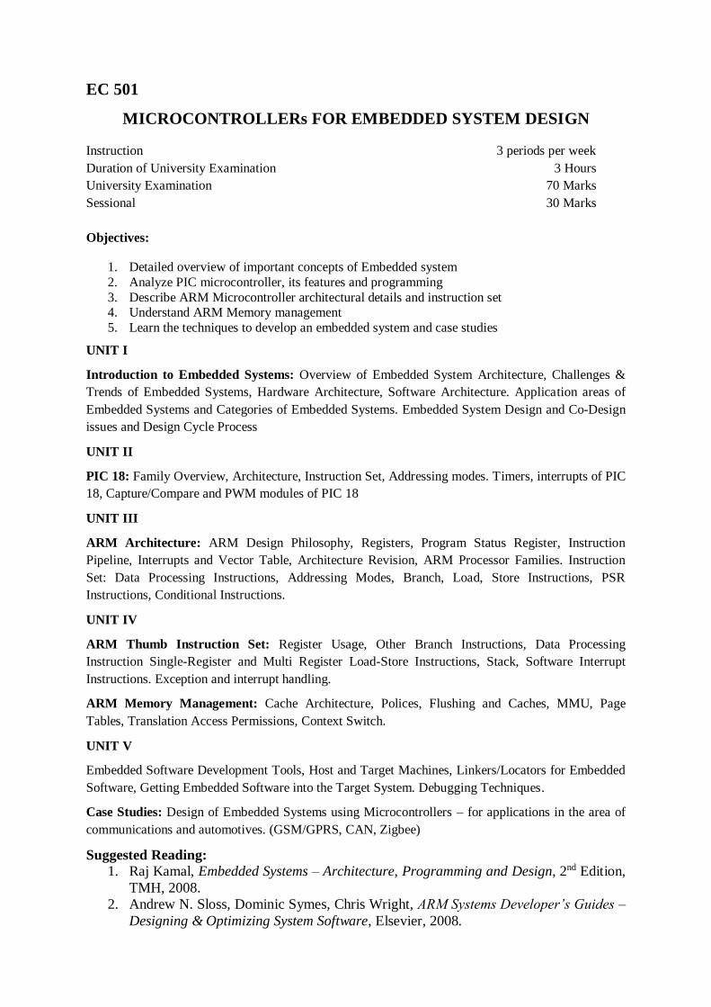
EC 501
MICROCONTROLLERs FOR EMBEDDED SYSTEM DESIGN
Instruction 3 periods per week
Duration of University Examination 3 Hours
University Examination 70 Marks
Sessional 30 Marks
Objectives:
1. Detailed overview of important concepts of Embedded system
2. Analyze PIC microcontroller, its features and programming
3. Describe ARM Microcontroller architectural details and instruction set 4. Understand ARM Memory management
5. Learn the techniques to develop an embedded system and case studies
UNIT I
Introduction to Embedded Systems: Overview of Embedded System Architecture, Challenges &
Trends of Embedded Systems, Hardware Architecture, Software Architecture. Application areas of
Embedded Systems and Categories of Embedded Systems. Embedded System Design and Co-Design
issues and Design Cycle Process
UNIT II
PIC 18: Family Overview, Architecture, Instruction Set, Addressing modes. Timers, interrupts of PIC
18, Capture/Compare and PWM modules of PIC 18
UNIT III
ARM Architecture: ARM Design Philosophy, Registers, Program Status Register, Instruction
Pipeline, Interrupts and Vector Table, Architecture Revision, ARM Processor Families. Instruction
Set: Data Processing Instructions, Addressing Modes, Branch, Load, Store Instructions, PSR
Instructions, Conditional Instructions.
UNIT IV
ARM Thumb Instruction Set: Register Usage, Other Branch Instructions, Data Processing
Instruction Single-Register and Multi Register Load-Store Instructions, Stack, Software Interrupt
Instructions. Exception and interrupt handling.
ARM Memory Management: Cache Architecture, Polices, Flushing and Caches, MMU, Page
Tables, Translation Access Permissions, Context Switch.
UNIT V
Embedded Software Development Tools, Host and Target Machines, Linkers/Locators for Embedded
Software, Getting Embedded Software into the Target System. Debugging Techniques.
Case Studies: Design of Embedded Systems using Microcontrollers – for applications in the area of
communications and automotives. (GSM/GPRS, CAN, Zigbee)
Suggested Reading: 1. Raj Kamal, Embedded Systems – Architecture, Programming and Design, 2nd Edition,
TMH, 2008.
2. Andrew N. Sloss, Dominic Symes, Chris Wright, ARM Systems Developer’s Guides –
Designing & Optimizing System Software, Elsevier, 2008.

3. Mazidi, MCKinlay and Danny Causey, PIC Microcontrollers and Embedded Systems,
Pearson Education, 2007
4. David.E.Simon, An Embedded Software Primer, 1st Edition, Pearson Education, 1999.
5. Jonathan W. Valvano, Embedded Microcomputer Systems, Real Time Interfacing,
Thomas Learning, 1999.

EC 502
DIGITAL SYSTEM DESIGN
Instruction 3 periods per week
Duration of University Examination 3 Hours
University Examination 70 Marks
Sessional 30 Marks
Objectives:
1. Design combinational logic circuits using PLDs and model sequential circuits as finite
state machines
2. Synthesize synchronous sequential circuits and fundamental mode asynchronous
sequential circuits
3. Realize digital systems in terms of State Machines (SM) charts 4. Model logical faults for combinational circuits using conventional test generation methods 5. Learn basic fault diagnosis algorithms in sequential circuits
UNIT I
Digital Design: Top-Down Modular Combination Logic Design, Combinational circuit Design with Programmable
logic Devices (PLDs).
Sequential circuits design: state table, state diagrams. Latches and Flip-Flops- excitation table, characteristic equations - Mealy, Moore models and Sequence detector
UNIT II
Minimization and Transformation of Sequential Machines: The Finite State Model – Capabilities and limitations of FSM – State equivalence and machine
minimization – Simplification of incompletely specified machines.
Fundamental mode model – Flow table, State reduction, Minimal closed covers – Races, Cycles and
Hazards.
UNIT III
State Machine Charts:
State machine charts, Derivation of SM Charts - Implementation of Binary Multiplier, Realization of SM Chart- Robot controller and Coin operated candy machine design..
UNIT IV
Fault Modelling & Test Pattern Generation:
Logic Fault model in combinational circuits – Fault detection and Redundancy, Fault equivalence and fault location, Fault dominance, Single stuck at fault model.
Fault diagnosis of combinational circuits by conventional methods – Path sensitization techniques,
Boolean Difference method, and D algorithm. Test generation - Random testing, Transition count testing and Signature analysis.
UNIT V
Fault Diagnosis in Sequential Circuits: Circuit Test Approach, Transition Check Approach – State identification and fault detection
experiment, Machine identification, Design of Fault detection experiment.
Suggested Reading: 1. John F. Wakerly, Digital Design, Principle and Practices, 3rd Edition, Pearson Education,
2003.
2. CD Victor, P. Nelson, H Troy Nagle, Bill D. Carrol and J David Irwin. Digital Logic Circuit Analysis and Design, PHI, 1996.

3. Charles H. Roth, Fundamentals of Logic Design, 5th edition, Cengage Learning 2010.
4. Miron Abramovici, Melvin A. Breuer and Arthur D. Friedman, Digital Systems Testing and Testable Design, John Wiley & Sons Inc 1990.
5. Parag.K.Lala, Fault Tolerant and Fault Testable Hardware Design, BS Publications, 2007.
6. Biswas N.N. Logic Design Theory, PHI, 2001. 7. Zvi Kohavi, Switching and Finite Automata Theory, TMH, 2001.
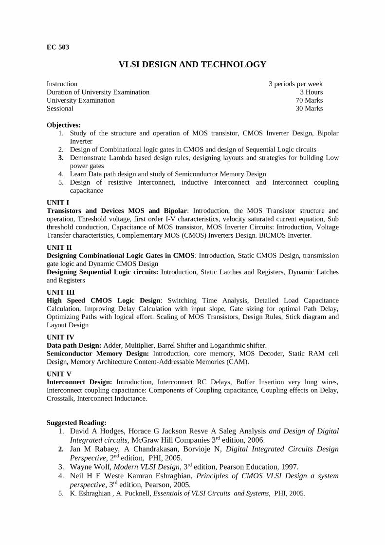
EC 503
VLSI DESIGN AND TECHNOLOGY
Instruction 3 periods per week
Duration of University Examination 3 Hours
University Examination 70 Marks Sessional 30 Marks
Objectives:
1. Study of the structure and operation of MOS transistor, CMOS Inverter Design, Bipolar Inverter
2. Design of Combinational logic gates in CMOS and design of Sequential Logic circuits
3. Demonstrate Lambda based design rules, designing layouts and strategies for building Low power gates
4. Learn Data path design and study of Semiconductor Memory Design
5. Design of resistive Interconnect, inductive Interconnect and Interconnect coupling
capacitance
UNIT I
Transistors and Devices MOS and Bipolar: Introduction, the MOS Transistor structure and
operation, Threshold voltage, first order I-V characteristics, velocity saturated current equation, Sub threshold conduction, Capacitance of MOS transistor, MOS Inverter Circuits: Introduction, Voltage
Transfer characteristics, Complementary MOS (CMOS) Inverters Design. BiCMOS Inverter.
UNIT II Designing Combinational Logic Gates in CMOS: Introduction, Static CMOS Design, transmission
gate logic and Dynamic CMOS Design
Designing Sequential Logic circuits: Introduction, Static Latches and Registers, Dynamic Latches
and Registers
UNIT III
High Speed CMOS Logic Design: Switching Time Analysis, Detailed Load Capacitance
Calculation, Improving Delay Calculation with input slope, Gate sizing for optimal Path Delay, Optimizing Paths with logical effort. Scaling of MOS Transistors, Design Rules, Stick diagram and
Layout Design
UNIT IV
Data path Design: Adder, Multiplier, Barrel Shifter and Logarithmic shifter. Semiconductor Memory Design: Introduction, core memory, MOS Decoder, Static RAM cell
Design, Memory Architecture Content-Addressable Memories (CAM).
UNIT V Interconnect Design: Introduction, Interconnect RC Delays, Buffer Insertion very long wires,
Interconnect coupling capacitance: Components of Coupling capacitance, Coupling effects on Delay,
Crosstalk, Interconnect Inductance.
Suggested Reading:
1. David A Hodges, Horace G Jackson Resve A Saleg Analysis and Design of Digital
Integrated circuits, McGraw Hill Companies 3rd edition, 2006.
2. Jan M Rabaey, A Chandrakasan, Borvioje N, Digital Integrated Circuits Design
Perspective, 2nd edition, PHI, 2005.
3. Wayne Wolf, Modern VLSI Design, 3rd edition, Pearson Education, 1997.
4. Neil H E Weste Kamran Eshraghian, Principles of CMOS VLSI Design a system
perspective, 3rd edition, Pearson, 2005. 5. K. Eshraghian , A. Pucknell, Essentials of VLSI Circuits and Systems, PHI, 2005.

EC 504
WIRELESS CHANNEL CODING TECHNIQUES
Instruction 3 periods per week
Duration of University Examination 3 Hours
University Examination 70 Marks Sessional 30 Marks
Objectives:
1. Describe performance of digital communication systems. Coding gain.
2. Design encoder and decoder for various coding schemes 3. Learn cyclic codes
4. Analysis of Performance improvement of convolution codes
5. Design of turbo encoder and decoder
UNIT I
Introduction:
Modulation and coding, Performance measures of coded modulation fields, Binary field arithmetic,
construction of Galois Field
UNIT II
Introduction to Linear block codes, the minimum distance of Block codes, Syndrome decoding,
Hamming codes, Reed-Muller codes, interleaved codes.
UNIT III
Cyclic codes, Generator and parity-check matrices of cyclic codes, Syndrome computation and error
detection. Binary BCH codes, Decoding of BCH codes and Reed Solomon codes.
UNIT IV
Convolutional Codes: Encoding of convolutional codes, Structural properties of convolutional codes.
The Viterbi algorithm and BCJR algorithm.
UNIT V
Turbo Coding: Introduction to turbo coding, Performance analysis of Turbo codes, Design of Turbo
codes, decoding of Turbo codes, Introduction to LDPC Codes, Tanner graph for Linear Block codes.
Suggested Reading:
1. Shu Lin, Daniel J., Costello, Jr., Error Control Coding, 2nd edition, Pearson, 2011.
2. Simon Haykin, Communication Systems, 4th Edition, John Wiley & Sons, 2007.
3. Proakis J.G. & M. Salehi, Digital Communications, Mc Graw-Hill, 2008.
4. Biglieri E., Coding for Wireless Channels, Springer, 2007.

EC 505
ADVANCED COMPUTER NETWORKS
Instruction 3 periods per week
Duration of University Examination 3 Hours
University Examination 70 Marks Sessional 30 Marks
Objectives:
1. Overview of computer networks, internet, and foundation of basic networking protocols. 2. Detailed study of Link layer, Routing and Congestion control at the network layer.
3. Learn Protocols in Network layer, Transport layer, and Application Layer.
4. Describe Concepts of Tunneling, VPN’s, Multimedia Networking Protocols, and Optical networks.
5. Overview of Wireless Networks, Mobile IP, Mobile A-Hoc and Wireless Sensor Networks
UNIT I
Computer Networks and the
Internet: What is the Internet, The Network edge, The Network core, Access Networks and Physical
media, ISPs and Internet Backbones, Delay and Loss in Packet-Switched Networks. Foundation of Networking Protocols: 5-layer TCP/IP Model, 7-Layer OSI Model, Internet
Protocols and Addressing, Equal-Sized Packets Model.
UNIT II
Link Layer and Local Area Networks: Introduction and Services, Error-Detection and Error-
Correction techniques, Multiple Access Protocols, LAN Addresses and ARP, Ethernet, Hubs, Bridges
and Switches, PPP: The Point-to-Point Protocol Wide Area Routing: Path Selection Algorithms - Dijkstra’s Algorithm, Bellman-Ford Algorithm,
Packet Flooding and Deflection Routing Algorithm.
Congestion Control at the Network Layer : Unidirectional Congestion Control, Bidirectional Congestion Control, Random Early Detection (RED).
UNIT III
Network layer: Internet Protocol: Internetworking, IPv4, IPv6 Transition from IPv4 to IPv6
Multicast Routing and Protocols: Basic Definitions and Techniques, Internet Group Management
Protocol (IGMP).
Transport and End-to-End Protocols: User Datagram Protocol (UDP), Transmission Control
Protocol (TCP), Mobile Transport Protocols, TCP Congestion Control. Application Layer: The Web and HTTP, File Transfer: FTP, Electronic Mail in the Internet, Domain
Name System (DNS).
UNIT IV
Tunneling, VPN’s and MPLS Networks – Tunneling, Virtual Private Networks (VPNs),
Multiprotocol Label Switching (MPLS).
Multimedia Networking - Protocols for Real – Time Interactive Applications – RTP, RTCP, SIP,
and H.323. Overview of Voice over IP, SIP to H.323, SIP to PSTN, Wireless Cellular Multimedia
Internetworking.
Optical Networks and WDM Systems: Overview of Optical Networks, Basic Optical Networking
Devices, Large-Scale Optical Switches, Optical Routers, Wavelength Allocation in Networks, Case
Study: An All-Optical Switch.

UNIT V
Wireless Networks and Mobile IP: Infrastructure of Wireless Networks, Wireless LAN Technologies, IEEE 802.11 Wireless Standard, Cellular Networks, Mobile IP, Wireless Mesh
Networks (WMNs). Mobile A-Hoc Networks: Overview of Wireless Ad-Hoc Networks, Routing in
Ad-Hoc Networks, Routing Protocols for Ad-Hoc Networks Wireless Sensor Networks: Sensor Networks and Protocol Structures, Communication Energy
Model, Clustering Protocols- LEACH Clustering and DEEP Clustering Protocol, Routing Protocols
Suggested Reading: 1. James F. Kurose, Keith W.Ross, Computer Networking: A Top-Down Approach Featuring
the Internet, 3rd Edition, Pearson Education, 2007
2. Nader F. Mir, Computer and Communication Networks, Pearson Education, 2007
3. Behrouz A. Forouzan, Data Communications and Networking, 4th Edition, Tata McGraw
Hill, 2007
4. Greg Tomsho,Ed Tittel, David Johnson, Guide to Networking Essentials, 5th Edition,
Thomson. 5. S.Keshav, An Engineering Approach to Computer Networking, Pearson Education.
6. Diane Teare, Catherine Paquet, Campus Network Design Fundamentals, Pearson Education
(CISCO Press) 7. Andrew S. Tanenbaum, Computer Networks, 4th Edition, Prentice Hall.
8. William Stallings, Data and Computer Communications, 8th Edition, Pearson Prentice Hall,
2007.

EC 506
DIGITAL SIGNAL PROCESSORS
Instruction 3 periods per week
Duration of University Examination 3 Hours
University Examination 70 Marks Sessional 30 Marks
Objectives:
1. Analyse and synthesize signals
2. Compute errors caused by conversion 3. Describe functional blocks of DSP processor and their use
4. Understand processors with examples
5. Design various interfacing devices with processor
UNIT I: Introduction to Digital Signal Processing: A Digital signal-processing system,
The sampling process, Discrete time sequences. Discrete Fourier Transform (DFT) and Fast
Fourier Transform (FFT), Linear time-invariant systems, Digital filters, Decimation and
interpolation.
UNIT II: Computational Accuracy in DSP Implementation: Number formats for signals
and coefficients in DSP systems, Dynamic Range and Precision, Sources of error in DSP
implementations, A/D Conversion errors, DSP Computational errors, D/A Conversion Errors,
Compensating filter.
UNIT III: Architectures for Programmable DSP Devices: Basic Architectural features,
DSP Computational Building Blocks, Bus Architecture and Memory, Data Addressing
Capabilities, Address Generation UNIT, Programmability and Program Execution, Speed
Issues, Features for External interfacing. Hardware looping, Interrupts, Stacks, Relative
Branch support, Pipelining and Performance, Pipeline Depth, Interlocking, Branching effects,
Interrupt effects, Pipeline Programming models.
UNIT IV: Programmable Digital Signal Processors: Commercial Digital signal-processing
Devices: : Fixed point DSPs – Architecture of TMS 320C5X, C54X Processors , addressing
modes, Memory space, Assembly instructions, Program Control ,Pipelining and on-chip
peripherals. Floating point DSPs: Architecture of TMS 320 – IX.
UNIT V: Interfacing Memory and I/O Peripherals to Programmable DSP Devices :
Memory space organization, External bus interfacing signals, Memory interface, Parallel I/O
interface, Programmed I/O, Interrupts and I/O, Direct memory access (DMA). A
Multichannel buffered serial port (McBSP), McBSP Programming, a CODEC interface
circuit, CODEC programming, A CODEC-DSP interface example.
Suggested Reading:
1. K. Shin, DSP Applications with TMS 320 Family, Prentice Hall, 1987.
2. B. Ventakaramani, M. Bhaskar, Digital Signal Processes, Architecture Processing
and Applications, Tata Mc Graw Hill, 2002.
3. Lapsley et al., DSP Processor Fundamentals, Architectures & Features, S. Chand &
Co, 2000.
4. Avtar Singh and S. Srinivasan, Digital Signal Processing, Thomson Publications,
2004.
5. Woon-Seng Gan, Sen M. Kuo, Embedded Signal Processing with the Micro Signal
Architecture, Wiley-IEEE Press, 2007.
6. C. Marren & G. Ewess, A Simple Approach to Digital Signal Processing, Wiley Inter-
science, 1996.
7. R. Vijayarajeswaran, Ananthi.S, A Practical Approach to Digital Signal Processing,
New Age International, 2009

EC 507
DIGITAL SYSTEMS LAB –I
Instruction 3 periods per week
Sessional 50 Marks
SECTION 1:
MICROPROCESSOR & MICROCONTROLLER
PART-A
1. Simple Assembly Language Program for: a) Addition/Subtraction/Multiplication/Division.
b) Operating modes, System calls and Interrupts.
c) Loops, Branches. 2. Assembly Language programs to configure and control general purpose I/O (GPIO) port pins.
3. Assembly Language programs to read digital values from external peripherals and execute them
with the Target board.
4. Program for reading and writing of a file.
5. Program to demonstrate Time delay Program using built in Timer/Counter feature on IDE
environment. 6. Program to demonstrate a simple interrupt handler and setting up a timer.
PART-B
INTERFACING EXPERIMENTS USING ARM DEVELOPMENT BOARD i) Program to interface 8-Bit LED and switch interface.
ii) Program to implement Buzzer interface on IDE environment.
iii) Program to display message in a 2 line x 16 characters LCD display and verify the result in debug terminal.
iv) Stepper motor interface.
v) ADC & Temperature sensor LM35 interface.
vi) Transmission from kit and reception from PC using serial port.
SECTION-2:
COMPUTER EXPERIMENTS USING MATLAB
1. Setting up advanced control program using SIMULINK 2. Time response of non Linear systems.
3. Creating frequency domain plots.
4. Performing state space communication and study of controllers and observers.
5. Implementation of Multirate systems. 6. Experiments using DSP Processor
i) Convolution & Correlation
ii) FIR Filtering iii) IIR Filtering
Note:
i) The following programs are to be implemented on ARM based processors/Equivalent. ii) Minimum of four programs from Part-A and four programs from Part-B are to be considered in
section-I

EC 508
DIGITAL SYSTEMS LAB –II
Instruction 3 periods per week
Sessional 50 Marks
Section - 3:
Part (a):
VHDL/Verilog
VHDL (or Verilog HDL) modeling, Simulation, Synthesis, Timing Analysis and
implementation on FPGA/CPLD target devices.
i. Combinational Circuits
ii. Sequential Circuits and FSMs
iii. Case study (Complete FPGA design flow including on-chip debugging)
Suggested Tools: Xilinx ISE/Altera Quartus, Modelsim/Active HDL and Target boards.
Section - 4:
VLSI Design
i. Design of CMOS Inverter & NAND Gate.
ii. Design of Half Adder using NAND Gates & Full Adder Design using Half
Adder.
iii. Design of 4-bit Adder using Full Adder.
iv. Design of 4-bit thermometer to Binary Code converter.
v. Layout Designs of above Digital Circuits.
Part (b):
Mini Project

EC 509
SEMINAR - I
Instruction 3 periods per week
Sessional 50 Marks
Oral presentation and technical report writing are two important aspect of engineering
education. The objective of the seminar is to prepare the student for a systematic and
independent study of the state of the art topics in the advanced fields of Communication
Engineering and related topics.
Seminar topics may be chosen by the students with advice from the faculty members.
Students are to be exposed to the following aspects for a seminar presentation.
Literature survey
Organization of the material
Presentation of OHP slides / LCD presentation
Technical writing
Each student required to:
1. Submit a one page synopsis before the seminar talk for display on the notice board.
2. Give a 20 minutes time for presentation following by a 10 minutes discussion.
3. Submit a detailed technical report on the seminar topic with list of references and slides
used.
Seminars are to be scheduled from the 3rd week to the last week of the semester and any
change in schedule shall not be entertained.
For award of sessional marks, students are to be judged by at least two faculty members on
the basis of an oral and technical report preparation as well as their involvement in the
discussions.

EC 510
SEMINAR - II
Instruction 3 periods per week
Sessional 50 Marks
Oral presentation and technical report writing are two important aspect of engineering
education. The objective of the seminar is to prepare the student for a systematic and
independent study of the state of the art topics in the advanced fields of Communication
Engineering and related topics.
Seminar topics may be chosen by the students with advice from the faculty members.
Students are to be exposed to the following aspects for a seminar presentation.
Literature survey
Organization of the material
Presentation of OHP slides / LCD presentation
Technical writing
Each student required to:
1. Submit a one page synopsis before the seminar talk for display on the notice board.
2. Give a 20 minutes time for presentation following by a 10 minutes discussion.
3. Submit a detailed technical report on the seminar topic with list of references and slides
used.
Seminars are to be scheduled from the 3rd week to the last week of the semester and any
change in schedule shall not be entertained.
For award of sessional marks, students are to be judged by at least two faculty members on
the basis of an oral and technical report preparation as well as their involvement in the
discussions.

EC 511
PROJECT SEMINAR Instruction 3 periods per week
Sessional 100 Marks
The main objective of the Project Seminar is to prepare the students for the dissertation to be
executed in 4th semester. Solving a real life problem should be focus of Post Graduate
dissertation. Faculty members should prepare the project briefs (giving scope and reference)
at the beginning of the 3rd semester, which should be made available to the students at the
departmental library. The project may be classified as hardware / software / modeling /
simulation. It may comprise any elements such as analysis, synthesis and design.
The Department will appoint a project coordinator who will coordinate the following:
Allotment of projects and project guides.
Conduct project - seminars.
Each student must be directed to decide on the following aspects
Title of the dissertation work.
Organization.
Internal / External guide.
Collection of literature related to the dissertation work.
Each student must present a seminar based on the above aspects as per the following
guidelines:
1. Submit a one page synopsis before the seminar talk for display on the notice board.
2. Give a 20 minutes presentation through OHP, PPT followed by a 10 minutes discussion.
3. Submit a report on the seminar presented giving the list of references.
Project Seminars are to be scheduled from the 3rd week to the last week of the semester. The
internal marks will be awarded based on preparation, presentation and participation.

EC 512
DISSERTATION
University Examination Grade
The students must be given clear guidelines to execute and complete the project on which
they have delivered a seminar in the 3rd semester of the course.
All projects will be monitored at least twice in a semester through student’s presentation.
Sessional marks should be based on the grades/marks, awarded by a monitoring committee of
faculty members as also marks given by the supervisor.
Efforts be made that some of the projects are carries out in industries with the help of
industry coordinates.
Common norms will be established for documentation of the project report by the respective
Department.
The internal viva voce exam must be conducted by a committee containing of the concerned
Head, senior faculty member, Chairman BoS or nominee and the supervisor. The draft thesis
must be submitted as per the almanac directed by the Dean, Faculty of Engineering, OU.
The project works must be evaluated by conducting an external viva-voce exam with the
committee containing an external examiner, concerned Head, Chairman BoS and the
supervisor.
+ Excellent /Very Good / Good/Satisfactory / Unsatisfactory

EC 520
ADVANCED COMPUTER ORGANIZATION
Instruction 3 periods per week
Duration of University Examination 3 Hours University Examination 70 Marks
Sessional 30 Marks
Objectives:
1. Design CPU organization, Data representation, Pipelining, Superscalar architectures
2. Learn Hardwired and Micro-Programmed Control UNIT Design 3. Understand memory organization and hierarchy
4. Describe IO interfacing concepts
5. Learn concepts, challenges and limitations of Instruction Level Parallelism (ILP)
UNIT I
Processor Design:
CPU Organization, Data Representation, Instruction Formats, Data Path Design: Fixed Point
Arithmetic and Floating Point Arithmetic, Instruction Pipelining, Super Scalar techniques, Linear
pipeline processors, Super scalar and super pipeline design, Multi vector and SIMD computers.
UNIT II
Control UNIT Design:
Basic Concepts: Hardwired Control UNIT Design approach, Micro-programmed Control UNIT
Design Approach, Micro program sequencer, Case studies based on both the approaches.
UNIT III
Memory Organization:
Internal memory, computer memory system overview, The memory Hierarchy, Random access
memories, Cache memory, Elements of cache design, Virtual memory- protection and examples of
virtual memory, Replacement Policies.
UNIT IV
I-O Organization:
Accessing I/O Devices, Programmed I-O, Interrupts, DMA, Bus Arbitration; Synchronous bus and
asynchronous bus, Interface circuits, Parallel port, Serial port, standard I/O interfaces, IO Processor,
PCI bus, SCSI bus, USB bus protocols.
UNIT V
Parallel Computer Systems:
Instruction Level Parallelism (ILP) – Concept and Challenges, Dynamic Scheduling, Limitations on
ILP, Thread Level Parallelism, Multi-processors – Characteristics, Symmetric and Distributive Shared
Memory Architecture, Vector Processors and Super computers.
Suggested Reading:
1. Hayes John P; Computer Architecture and Organization; 3rd Edition, MGH, 1998.
2. John L. Hennessy and David A. Patterson, Computer Architecture – A quantitative Approach,
3rd Edition, Elsevier, 2005. 3. William Stallings, Computer Organization and Architecture designing for Performance, 7th
edition, PHI, 2007.
EC 521
ADVANCED DIGITAL DESIGN WITH VERILOG HDL
Instruction 3 periods per week Duration of University Examination 3 Hours
University Examination 70 Marks
Sessional 30 Marks
Objectives:
1. Describe modelling styles of Verilog HDL
2. Design modelling of Combinational and Sequential Logic modules
3. Learn synthesis and synthesizers
4. Understand verification methods and timing analysis
5. Demonstrate case studies using Verilog HDL
UNIT I
Review of Verilog HDL, Modelling styles: Behavioural, Dataflow, and Structural Modelling,
gate delays, switch-level Modelling, Hierarchal structural modelling.
UNIT II
Modelling of basic MSI Combinational Logic modules and Sequential Logic modules. Finite
State Machine modelling.
UNIT III
Synthesis: Design flow of ASICs and FPGA based system, design environment and
constraints logic synthesizers, Language structure synthesis, coding guidelines for clocks and
reset.
UNIT IV
Verification: Functional verification, simulation types, Test Bench design, Dynamic timing
analysis, static timing analysis, value change dump (VCD) files. FPGA based design flow- a
case study.
UNIT V
Design Examples: Adders and Subtractors, Multiplication and Division Algorithms, ALU,
Digital Signal Processing modules: FIR and IIR Filters, Bus structures, Synchronous &
Asynchronous data transfer, UART, baud rate generator. A simple CPU design
Suggested Reading:
1. Ming-Bo Lin., Digital System Designs and Practices Using Verilog HDL and FPGAs.
Wiley, 2008.
2. Michael D. Ciletti, Advanced Digital Design with the Verilog HDL”, PHI, 2005.
3. Samir Palnitkar, “Verilog HDL: A Guide to Digital Design and Synthesis”, Pearson
Education, 2005.
4. Bhasker J., Verilog HDL Primer Hardcover, 2nd Edition, Star Galaxy Publishing ,1999

EC 522
FIELD PROGRAMMABLE GATE ARRAYS
Instruction 3 periods per week
Duration of University Examination 3 Hours University Examination 70 Marks
Sessional 30 Marks
Objectives:
1. Learn Application Specific IC (ASIC) fundamentals
2. Describe FPGA
3. Calculate power consumption of designed IC
4. Understand Interconnection, Placement and Routing schemes.
5. Learn Verification and testing schemes. m
UNIT I
Introduction to ASIC’s: Types of ASIC’s, ASIC design flow, Economies of ASIC’s,
Programmable ASIC’s: CPLD and FPGA. Commercially available CPLD’s and FPGA’s:
XILINX, ALTERA, ACTEL. FPGA Design cycle, Implementation tools: Simulation and
synthesis, Programming technologies. Applications of FPGAs
UNIT II
FPGA logic cell for XILINX, ALTERA and ACTEL ACT, Technology trends,
Programmable I/O blocks, FPGA interconnect: Routing resources, Elmore’s constant, RC
delay and parasitic capacitance, FPGA design flow, Dedicated Specialised components of
FPGAs
UNIT III
FPGA physical design, CAD tools, Power dissipation, FPGA Partitioning, Partitioning
methods. Floor planning: Goals and objectives, I/O, Power and clock planning, Low-level
design entry.
UNIT IV
Placement: Goals and objectives, Placement algorithms: Min-cut based placement, Iterative
Improvement and simulated annealing.
Routing, introduction, Global routing: Goals and objectives, Global routing methods, Back-
annotation. Detailed Routing: Goals and objectives, Channel density, Segmented channel
routing, Maze routing, Clock and power routing, Circuit extraction and DRC.
UNIT V
Verification and Testing: Verification: Logic simulation, Design validation, Timing
verification. Testing concepts: Failures, Mechanism and faults, Fault coverage. Design
Applications: General Design issues, Counter Examples, A Fast DMA controller, Designing
adders and accumulators with Xilinx Architecture.

Suggested reading:
1. Pak and Chan, Samiha Mourad, Digital Design using Field Programmable Gate
Arrays, Pearson Education, 1st edition, 2009.
2. Michael John Sebastian Smith, Application Specific Integrated Circuits, Pearson
Education Asia, 3rd edition 2001.
3. S. Trimberger, Edr, Field Programmable Gate Array Technology, Kluwer Academic
Publications, 1994.
4. John V.Oldfield, Richard C Dore, Field Programmable Gate Arrays, Wiley
Publications.

EC 523
MULTIMEDIA INFORMATION SYSTEMS
Instruction 3 periods per week
Duration of University Examination 3 Hours
University Examination 70 Marks Sessional 30 Marks
Objectives:
1. Describe information on digital media
2. Outline networking synchronization of various systems
3. Study methods of computation, analyze various models
4. Study methods for interfacing different systems with different sampling ratio
5. Learn reconstruction of signals, coding and decoding
UNIT I
Definition of Multimedia, Multimedia system description. Applications of Multimedia.
Types of Multimedia: a non-interactive, interactive. Hypertext.
UNIT II
Multimedia Networking: ATM. ISDN. WAN and their comparisons, Multimedia
synchronization. Serial and Parallel.
UNIT III
Motion estimation techniques: Bruteforce, algorithm three step, search algorithm. 2-D
algorithm and conjugate direction search algorithm.
Image compression standards: Review on loseless and lossy compression models.JPEG.H261
MPEG1, MPEG2 and MPEG4.
UNIT IV
Audio coding: Introduction to multi rate signals. MPEG1 and MPEG2 audio encoder and
decoder.
UNIT V
Multimedia information indexing and Retrieval: General information Retrieval (IR) model.
Differences between IR and DBMS Basic IR models. File structure, audio indexing and
Retrieval methods. Image Retrieval based on shape and moments and watermarking
Techniques.
Suggested Reading:
1. Guojun Lu, Communication and Computing for distributed multimedia systems,
Artech House, Boston, London, 1995.
2. Bhaskar, V and Konstantindes K, Image and Video Compression Standards
algorithms and Architecture, Kluwer Academic, Sept, 1997.
3. Judith Jeffocate, Printmedia in practice (Theory and Applications), PHI, 1998.

EC 524
SPEECH SIGNAL PROCESSING
Instruction 3 periods per week
Duration of University Examination 3 Hours University Examination 70 Marks
Sessional 30 Marks
Objectives:
1. Describe speech production and perception and modelling
2. Analyze speech signal and computation
3. Represent speech with models
4. Represent speech with coders, encoders and decoders
5. Learn Automatic Speech Recognition
UNIT I
The process of speech production: Production Mechanism and acoustic phonetics. Digital
models for speech signals: Vocal Tract, Radiation, Excitation and complete model speech
perception: Loudness, Bark Scale, masking, perception and Psychoacoustics.
UNIT II
Short-time Period analysis: Short-time energy, Average magnitude, zero crossing, Speech
vs Silence discrimination and zero crossing rate, Pitch period estimation using parallel
processing approach. Autocorrelation function, Pitch period estimation using Auto
correlation function, The average magnitude function, median smoothing. Short time Fourier
Analysis: Fourier transform interpretation, linear filtering interpretation, sampling rates in
time and frequency, Filter banks, Spectctrograms, pitch detection. Cepstral analysis, Complex
and real cepstrum, pitch detection and Formant estimation.
UNIT III
Digital Models for Speech Signals: Review of PCM, adaptive PCM, differential PCM, delta
modulation. Linear Predictive coding (LPC) analysis: Basic principles, autocorrelation and
covariance methods, Computation of LP coefficients, Cholesky decomposition, Durbin’s
recursive solution, Frequency domain interpretation of LPC, CELP.
UNIT IV
Analysis by Synthesis: Phase vocoder, subband coding, Formant /homomorphic vocoder,
cepstral vocoder, vector quantizer coder, Speech enhancement techniques: Spectral
subtraction, enhancement by resynthesis.
UNIT V
Automatic speech recognition: Basic pattern recognition approaches, evaluating the
similarity of speech patterns, Dynamic Time Warping (DTW), HMM’s for speech
recognition, forward, backward algorithms and parameter estimation. Speaker recognition,
Features that distinguish speakers.
Suggested Readings:
1. Rabinar and Schafer, Digital Processing of Speech Signals, Pearson Education, 2004.
2. Deller, Hansen, Proakis, Discrete-Time Processing of Speech signals, IEEE presses,
2000.
3. R & J Rabinar and Juang, Fundamentals of speech recognition, Prentice Hall, 1993.
4. Douglas O’Shaughnessy, Speech Communication: Human and Machine, 2nd edition,
University Press, Hyderabad, 2001.

EC 525
IMAGE AND VIDEO PROCESSING
Instruction 3 periods per week
Duration of University Examination 3 Hours University Examination 70 Marks
Sessional 30 Marks
Objectives: 1. Study fundamental concepts of Image Processing and various Image Transforms
2. Learn Image Enhancement Techniques in Spatial and Frequency domain, Image
Segmentation methods 3. Familiarize with fundamentals of Image compression, Lossy & Lossless Compression
methods.
4. Define concepts of Video Processing, Image Formation models, and processing of Video signals.
5. Understand general methodologies of 2 D Motion Estimation and Video coding methods.
UNIT I
Fundamentals of Image Processing and Image Transforms Basic steps of Image Processing System, Sampling and Quantization of an image, relationship
between pixels
Image Transforms: 2 D- Discrete Fourier Transform, Discrete Cosine Transform (DCT), Wavelet Transforms: Continuous Wavelet Transform, Discrete Wavelet Transforms.
UNIT II
Image Processing Techniques
Image Enhancement Spatial domain methods: Histogram processing, Fundamentals of Spatial filtering, Smoothing spatial
filters, Sharpening spatial filters.
Frequency domain methods: Basics of filtering in frequency domain, image smoothing, image sharpening, Selective filtering. Laplacian of Gaussian (LOG) filters.
Image Segmentation
Segmentation concepts, Point, Line and Edge Detection, Thresholding , Region Based segmentation, Hough Transform, Boundary detection, chain coding.
UNIT III
Image Compression
Image compression fundamentals - Coding Redundancy, Spatial and Temporal redundancy, Compression models: Lossy & Lossless, Huffman coding, Arithmetic coding, LZW coding, Run
length coding, Bit plane coding, Transform coding, Predictive coding, Wavelet coding, JPEG
Standards.
UNIT IV
Basic concepts of Video Processing
Analog Video, Digital Video. Time-Varying Image Formation models: Three-Dimensional Motion Models, Geometric Image Formation, Photometric Image Formation, Sampling of Video signals,
Filtering operations.
UNIT V
2-D Motion Estimation Optical flow, General Methodologies, Pixel Based Motion Estimation, Block- Matching Algorithm,
Mesh based Motion Estimation, Global Motion Estimation, Region based Motion Estimation, Multi
resolution motion estimation, Waveform based coding, Block based transform coding, Predictive
coding, Application of motion estimation in Video coding, constant dependent video coding and joint
shape and texture coding .MPEG and H.26X standards.
Suggested Reading:
1. Gonzaleze and Woods, Digital Image Processing, 3rd edition, Pearson. 2. Yao Wang, Joem Ostermann , Ya–quin Zhang, Video processing and communication, 1st Edition,
PH Int.
3. S.Jayaraman, S.Esakkirajan, T.Veera Kumar Digital Image Processing, TMH, 2009. 4. M. Tekalp, Digital Video Processing, Prentice Hall International
5. John Woods, Multi-dimensional Signal, Image and Video Processing and Coding 2nd Edition,
Elsevier. 6. Vipula Singh, Digital Image Processing with MATLAB and LabVIEW, Elsevier, 2013
7. Keith Jack, Video Demystified – A Hand Book for the Digital Engineer, 5th Edition, Elsevier.

EC 526
OPTIMIZATION TECHNIQUES
Instruction 3 periods per week
Duration of University Examination 3 Hours University Examination 70 Marks
Sessional 30 Marks
Objectives: 1. Obtain the best result under given circumstances using optimization methods
2. Learn various search methods for evaluation
3. Determine optimum value and universal value
4. Review of global optimization techniques 5. Understand generic algorithms
UNIT I
Use of optimization methods. Introduction to classical optimization techniques, motivation to
the simplex method, simplex algorithm, sensitivity analysis.
UNIT II
Search methods - Unrestricted search, exhaustive search, Fibonocci method, Golden section
method, Direct search method, Random search methods, Univariate method, simplex method,
Pattern search method.
UNIT III
Descent methods, Gradient of function, steepest decent method, conjugate gradient method.
Characteristics of constrained problem, Direct methods, The complex method, cutting plane
method.
UNIT IV
Review of a global optimization techniques such as Monte Carlo method, Simulated
annealing and Tunneling algorithm.
UNIT V
Generic algorithm - Selection process, Crossover, Mutation, Schema theorem, comparison
between binary and floating point implementation.
Suggested Reading:
1. SS Rao, “Optimization techniques”, PHI, 1989.
2. Zhigmiew Michelewicz, “Genetic algorithms + data structures = Evaluation programs”,
Springer Verlog - 1992.
3. Merrium C. W., “Optimization theory and the design of feedback control systems”,
McGraw Hill, 1964.
4. Weldo D.J., “Optimum seeking method”, PHI, 1964.

EC 527
Mobile Ad-hoc and Sensor Networks
Instruction 3 periods per week
Duration of University Examination 3 Hours University Examination 70 Marks
Sessional 30 Marks
Objectives:
1. Outline of sensing, computing and communication elements
2. Describe Data dissemination and accumulation, catching and storage
3. Detection of signal topology, management and topological routing. Dispersed sensors
covering geographic area
4. Learn Synchronization of signals and recognition channel sharing and locality
5. Understand Identification and error detection and routing of signals, sensor nodes
have limited energy, limited communication and computational capabilities and
limited memory
UNIT I
Introduction: mobile ad hoc networks (MANETs) and wireless sensor networks (WSNs),
concepts and architectures, Routing: proactive routing, reactive routing (on demand), hybrid
routing, power-aware routing, Network simulators (OPNET, NS2, etc.)
UNIT II
Broadcasting and multicasting: broadcast storm, network flooding avoidance, multicast
routing, TCP over mobile ad hoc networks: IP address acquisition, effects of partitions on
TCP, provisions for mobility and fairness, Wireless LAN (WiFi): 802.11 specifications,
Medium Access Control Protocol issues; power control, spatial reusability, and QoS.
Bluetooth: specifications, Piconet synchronization and master-slave switch, scatter-net
formations, interference issues, interoperability with WiFi.
UNIT III
Wireless sensor networks (WSNs): single node architecture: hardware and software
components of a sensor node, Tiny OS operating system, nesC language, WSN Network
architecture: typical network architectures, data relaying strategies, aggregation, role of
energy in routing decisions, WSN MAC layer strategies: MAC layer protocols, energy
management, contention-based protocols, schedule-based protocols, 802.15.4 standard.
UNIT IV
WSN naming and addressing: addressing services, publish-subscribe topologies, WSN
Clock Synchronization: clustering for synchronization, sender-receiver and receiver-receiver
synchronization. Error analysis
UNIT V
WSN Node Localization: absolute and relative localization, triangulation, multi-hop
localization and error analysis, anchoring, geographic localization, WSN Routing: Agent-
based routing, random walk, trace routing.
Suggested Reading:
1. C.Siva Ram Murthy and B.S.Manoj, Ad Hoc Wireless Networks: Architectures and
Protocols, Prentice Hall PTR, 2007.
2. Holger Karl and Andreas Willig, Protocols and Architectures for Wireless Sensor
Networks, WILEY (ISBN: 0-470-09510-5)

3. C. Siva Ram Murthy and B. S. Manoj, Ad Hoc Wireless Networks: Architectures and
Protocol, Prentice Hall, 2004.
4. Feng Zhao and Leonidas J. Guibas, Wireless Sensor Networks: An Information Processing
Approach, Morgan Kaufmann, 2004
5. Kazem Sohraby, Daniel Minoli and Taieb Znati, Wireless Sensor Networks Technology-
Protocols and Applications, John Wiley & Sons, 2007.
6. Charles E. Perkins, Ad Hoc Networking, Addison Wesley, 2000.

EC 528
NEURAL NETWORKS AND FUZZY LOGIC
Instruction 3 periods per week
Duration of University Examination 3 Hours University Examination 70 Marks
Sessional 30 Marks
Objectives: 1. Formulate neural networks
2. Understand Training of neural networks using various algorithms
3. Use of neural networks for pattern recognition
4. Learn fuzzy systems, application of fuzzy systems 5. Describe Comparison of fuzzy systems with conventional control system.
UNIT I
Introduction:
Introduction to ANS (Artificial Neural systems) Technology, ANS simulation, Types of
Neural Networks: Hopfield, perceptron and related models, Adaline and Madaline: Adaline
and the Adaptive Linear Combiner, the Madaline and simulating the Adaline. Essential vector
operations, Lateral Inhibition and Sensory Processing.
UNIT II
Probabilistic Models, Fuzzy ARTMAP and Recurrent Networks:-Probabilistic Neural
Networks, General Regression Neural Networks, Fuzzy ARTMAP, Recurrent Back
propagation Neural Networks, Hybrid Learning Neural Networks:- Counter propagation
Network, Radial basis Function Networks.
UNIT III
Application of Neural Networks:-
Design and optimization of Systems: Non-Linear optimization, Inverse design problems,
Pattern Recognition Applications: Control Chart pattern Recognition, Recognition of
Machine-Cells in a group technology layout. Complex pattern Recognition tasks: Pattern
mapping, Temporal patters, pattern variability, Neocognitron, Addition of lateral inhibition
and Feedback to the Neocognitron.
UNIT IV
Introduction to Fuzzy systems, Fuzzy sets and operations on Fuzzy sets, Basics of Fuzzy
relations, Fuzzy measures, Fuzzy integrals, Transform Image coding with Adaptive Fuzzy
systems, Adaptive FAM systems for Transform coding.
UNIT V
Comparison of Fuzzy and Kalman-Filter Target, Tracking control systems, Fuzzy and Math-
Model Controllers, Real Time Target Tracking, Fuzzy Controller, Kalmaln-Filter Controller,
Fuzzified CMAC and RBF – Network based self learning Controllers.
Suggested Reading:
1. James A. Freeman and David M. Skapura, Neural Networks: Algorithms, Applications
and Programming Techniques, Pearson Education, India, 2008.
2. James A. Anderson, An introduction to Neural Networks, PHI, 2003.
3. B.Yegnanarayana, Artificial Neural Networks, PHI Publications India, 2006.
4. M.Ananda Rao and J.Srinivas, Neural Networks: Algorithms and Applications,
Narosa Publications 2009.
5. Timothy J.Ross Fuzzy Logic with Engineering Applications, McGraw Hill 2004.
6. Bart Kosko, Neural Networks and Fuzzy Systems, PHI India Publications, 2008.
7. Junhong Nie and Derek Linkens, Fuzzy – Neural Control, PHI India Publications,
1995

EC 529
MOBILE COMPUTING
Instruction 3 periods per week Duration of University Examination 3 Hours
University Examination 70 Marks
Sessional 30 Marks
Objectives:
1. Learn front end devices for information access and their operating systems.
2. Familiarize with Communication between the mobile equipment and the base station transceiver
3. Learn transmission and reception of data directory service
4. Formulate network routing
5. Estimate transaction.
UNIT I
Introduction: Challenges in mobile computing, coping with uncertainties, Resource
poorness, bandwidth, etc. Cellular architecture, co-channel interference, frequency reuse,
capacity increase by cell splitting: Evolution of mobile system: CDMA, FDMA, TDMA and
GSM.
UNIT II
Mobility Management: Cellular architecture, Co-channel interference, Mobility: handoff,
types of handoffs; Location management, HLR-VLR scheme, Hierarchial scheme, Predictive
location management schemes, Mobile IP, Cellular IP.
UNIT III
Publishing and Accessing Data in Air: Pull and Push based data delivery models, Data
dissemination by broadcast, Broadcast disks, Directory service in air, energy efficient
indexing scheme for push based data delivery.
File system support for mobility: Distributed file sharing for mobility support, Coda and other
storage manager for mobility support.
UNIT IV
Ad hoc Network Routing protocols: Ad hoc network routing protocols, destination
sequenced distance vector algorithm, Cluster based gate way switch routing, Global state
routing, fish- eye state routing, dynamic source routing, ad hoc on-demand routing, location
aided routing, Zonal routing algorithm.
UNIT V
Mobile Transaction and Commerce: Models for mobile transaction, Kangaroo and Joey
transactions, Team transaction, Recovery model for mobile transactions. Electronic payment
and protocols for mobile commerce.
Suggested Reading:
1. Jochen Schiller, Mobile Communications, 2nd edition, Pearson Education, 2004.
2. Hansmann, Merk, Nicklous, Stober, Principles of mobile Computing, 2nd edition,
Springer International Edition, 2003.
3. A Survey of Mobile transactions appeared in distributed and parallel data bases, 16,
193-230, 2004, Kluwer Academic Publishers.
4. S. Acharya, M.Franklin and S.Zdonik, Balancing Push and pull for Data Broadcast,
Proceedings of the ACM SIGMOD, Tuscon, AZ, May 1997.

EC 530
GLOBAL & REGIONAL NAVIGATION SATELLITE SYSTEMS
Instruction 3 periods per week
Duration of University Examination 3 Hours
University Examination 70 Marks
Sessional 30 Marks
Objectives:
1. Familiarize with GNNS fundamentals
2. Learn GNSS signal structure, errors and their modeling
3. Understand GPS errors and their modeling techniques
4. Study GPS integration and data processing techniques
5. Analyze GNSS augmentation and Regional navigation systems
UNIT I
GPS fundamentals: GPS principle of operation, architecture, operating frequencies, orbits,
Keplerian elements. Solar and Sidereal day, GPS and UTC Time
Other GNNSs: Architecture and features of Russian Global Navigation Satellite System
(GLONASS), European Navigation System (Galileo), Chinese Global Navigation System
(BeiDou-2/COMPASS).
UNIT II
GNSS Signals: Original and modernized GPS, GLONASS and Galileo signal structure,
Signal components and modulation schemes. Important components of a receiver for the
acquisition and tracking of GPS signals.
GNSS Datums: Datums used for GPS and Galileo (ECEF and WGS 84). Datum used by
Russian GLONASS and Indian Datums.
UNIT III
GPS Error Models: Ionospheric error, Tropospheric error, Ephemeris error, Clock errors,
Satellite and receiver instrumental biases, Antenna Phase center variation, multipath;
estimation of Total Electron Content (TEC) using dual frequency measurements, Various
DOPs, UERE. Spoofing and Anti-spoofing. Link budget. Klobuchar model, Hopfield model
and modeling of multipath error.
UNIT IV
GPS data processing: RINEX Navigation and Observation formats, Code and carrier phase
observables, linear combination and derived observables, Ambiguity resolution, cycle slips,
Position estimation.
GPS integration: GPS/GIS, GPS/INS, GPS/pseudolite, GPS/cellular.
UNIT V
Augmentation systems: Relative advantages of SBAS and GBAS, Wide area augmentation
system (WAAS) architecture, GAGAN, EGNOS and MSAS. Principle of operation of DGPS,
architecture and errors. Local area augmentation system (LAAS) concept.
Regional Navigation Satellite Systems (RNSS): Chinese Area Positioning System (CAPS).
Indian Regional Navigation Satellite System (IRNSS), Japan’s Quasi-Zenith Satellite System
(QZSS).

Suggested Reading:
1. Pratap Misra and Per Enge, Global Positioning System Signals, Measurements, and
Performance, Ganga-Jamuna Press, Massachusetts, 2001.
2. Rao G.S., Global Navigation Satellite Systems - With Essentials of Satellite
Communications, Tata McGraw Hill, 2010.
3. B.Hofmann Wollenhof, H.Lichtenegger, and J.Collins, GPS Theory and Practice,
Springer Wien, New York, 2000.
4. Ahmed El-Rabbany, Introduction to GPS, Artech House, Boston, 2002.
5. Bradford W. Parkinson and James J. Spilker, Global Positioning System: Theory and
Applications, Volume I and II, American Institute of Aeronautics and Astronautics,
Inc., Washington, 1996.
6. E-book available on: http://www.unoosa.org/pdf/publications/icg_ebook.pdf

EC 531
GNSS SIGNALS AND RECEIVER TECHNOLOGY
Instruction 3 periods per week
Duration of University Examination 3 Hours
University Examination 70 Marks
Sessional 30 Marks Objectives:
1. Locate user in GNSS available for positioning
2. Describe GNSS receiver hardware 3. Understand Signal generation, analysis, synthesis and modulation techniques
4. Learn Detection of signal and range calculations
5. Familiarize with Extraction of information from signal and mitigation of errors
UNIT I
Basic GPS Concept: Principle of Operation, Architecture, Space, control and user segments. Other
GNSS systems: GLONASS and Galileo. GPS Signal : Signals and Data, GPS Signal Scheme, C/A
Code, Gold Sequence, Gold Sequence Generation, Correlation Properties, Doppler Frequency Shift, Code Tracking, Navigation Data, Telemetry and Handover Words, Data in Navigation Message.
Galileo Signal: Galileo L1 OS Signal: Signal Generation, Coherent Adaptive Sub-carrier Modulation,
Binary Offset Carrier Modulation, and Message Structure: Frames and Pages Cyclic Redundancy Check, Forward Error Correction and Block Interleaving, Message Contents: Time and Clock
Correction Parameters, Conversion of GST to UTC and GPST, Service Parameters, the Received L1
OS Signal, GLONASS and other GNSS signals.
UNIT II
GNSS Receiver Operation Overview: Receiver Channels, Acquisition, Tracking, Navigation Data
Extraction, Computation of Position, GNSS Antennas and Front Ends: GNSS L1 Front-End
Components, GNSS Antenna, Filter, Amplifier, Mixer/Local Oscillator, Analog-to-Digital Converter, Resulting Sampled Data, GNSS Front-End ASICS.
UNIT III
Acquisition: Serial Search Acquisition, PRN Sequence Generation, Carrier Generation, Integration and Squaring, Parallel Frequency Space Search Acquisition, Parallel Code Phase Search Acquisition,
Data Size, Execution Time, Parameter Estimation.
UNIT IV
Carrier and Code Tracking: Motivation, Demodulation, Second-Order PLL, Damping Ratio, Noise Bandwidth, Carrier Tracking, Code Tracking, Multipath, Complete Tracking Block, Pseudo-range
Computations.
UNIT V Data Processing for Positioning, Navigation Data Recovery, Finding the Bit Transition Time and the
Bit Values, Navigation Data Decoding, Location of Preamble, Extracting the Navigation Data,
Computation of Satellite Position, Pseudo-range Estimation, The Initial Set of Pseudo-ranges, Estimation of Subsequent Pseudo-ranges, Computation of Receiver Position, Time, Linearization of
the Observation Equation, Using the Least-Squares Method, Real-Time Positioning Accuracy, Time
Systems Relevant for GPS, Coordinate Transformations, Universal Transverse Mercator Mapping,
Dilution of Precision, World Geodetic System 1984, Time and Coordinate Reference Frames for GPS and Galileo
Suggested Reading: 1. Kai Borre, Dennis M. Akos, Nicolaj Bertelsen, Peter Rinder, Søren Holdt Jensen, A Software-
Defined GPS and Galileo Receiver A Single-Frequency Approach, Birkhauser, Boston, 2007
2. James Bao-Yen Tsui, Fundamentals of global positioning system receivers: a software, Wiley Inter-science, 2005
3. Hofmann-Wellenhof, Bernhard, Lichtenegger, Herbert, Wasle, Elmar GNSS – Global
Navigation Satellite Systems: GPS, GLONASS, Galileo, and More, Springer, 2008.
EC 532
MODERN DIGITAL COMMUNICATION SYSTEMS
Instruction 3 periods per week
Duration of University Examination 3 Hours
University Examination 70 Marks
Sessionas 30 Marks
Objectives:
1. Represent communication channel as Band Pass system
2. Understand Transmission of data and equalization
3. Compare performance of MSK and Mary receiver
4. Learn Encryption and decryption of data
5. Analyze multipath fading
UNIT I
Characterization of Communication signals and systems: Bandpass signals, Linear
Bandpass systems and its response, Bandpass stationary stochastic processes, Power spectra
of linearly modulated signals.
UNIT II
Baseband Data Transmission: Correlative coding: Duobinary signalling, Duo-binary
decoding, Pre-coding, Duo-binary equivalent transfer function, Comparison of Binary with
Duo-binary signalling Poly-binary signalling, Inter symbol interference, Equalization.
UNIT III
Bandpass Data Transmission: Coherent and non-coherent modulation and detection of
digital (binary and M-ary) signals, Optimum Receiver, MSK, Mary signalling and
performances.
UNIT IV
Encryption and Decryption: A model of the encryption and decryption process, cipher
systems, stream encryption and public key encrypt systems.
UNIT V
Fading channel characteristics: channel characteristics, channel classification, channel
correlation function and power spectra, the effect signal characteristics on the choice of
channel model, Mitigation techniques for multipath fading channel: space diversity,
frequency diversity, time diversity, multipath diversity and RAKE Receiver, frequency
selective and non-selective fading, Example of Radio channels.
Suggested Reading:
1. John G. Proakis, Digital Communications, 4th edition, McGraw Hill international edition,
2001.
2. Bernard Sklar, Digital communications fundamentals and Application, 2nd edition,
Pearson education, 2001.
3. Fuqin Xiong, Digital modulation Techniques, Artech House, 2000.
4. Stephen G. Witson, Digital Modulation and Coding, Prentice Hall, New Jessey, 1996.
5. Rodger E. Ziemer and Roger L Peterson, Introduction to Digital communication, 2nd
edition, Prentice Hall International edition, 2001.

EC 533
OPTICAL FIBRE COMMUNICATION SYSTEMS
Instruction 3 periods per week
Duration of University Examination 3 Hours
University Examination 70 Marks
Sessional 30 Marks
Objectives:
1. Analyze optical fibre as wave guide
2. Learn various optical sources and detectors used in optical signal transmission
3. Familiarize with various components used in optical communication like,
preamplifiers, links
4. Estimate Performance evaluation of optical communication
5. Explore aapplications of optical communication in Local Area Networks
UNIT I Optical Fibres: Fibre Structures, Wave-guiding and fabrications, Overview of Optical
fibre communications, Elements of an Optical fibre transmission Link, Nature of
light, Basic optical laws and definitions, Modes and configurations, Mode theory of
circular wave guides, Single, Multi mode step index and Graded index Fibres , Fibre
materials. Signal degradation in Optical Fibres. Dispersion, Pulse broadening in
graded index fibres, Mode coupling, Design optimization of single mode Fibres.
UNIT II Optical Sources & Detectors: Semiconductors as optical Sources and their fabrication.
LED and Laser diodes, Linearity of sources, Modal, Partition and reflection noise,
Physical principles of PIN and APD, Photo detector noise, detector response time,
Avalanche multiplication noise, Temperature effect on avalanche gain, Comparison of
Photo detectors.
UNIT III Optical Fibre communication: Basic communication system, Fundamental receiver
operation, Digital receiver performance calculations. Preamplifiers types, Analog
receivers. Fibre Links: Point to point links, Line coding, Error correction, Noise
effects on digital transmission system performance. Overview of analog links, Carrier
noise ratio in analog systems.
UNIT IV
Multi channel transmission techniques: WDM concepts and components. Operational
principles of WDM, Passive components, Tunable sources, Tunable filters,
Introduction of optical amplifiers.
UNIT V Optical Networks: Basic Networks, SONET/SDH, Broadcast and select WDM
networks, Wavelength Routed Networks, Nonlinear effects on Network Performance,
Performance of EDFA+WDM systems, Optical CDMA, Ultrahigh capacity Networks.

Suggested Reading:
1. Djafar K.mynbaev Lowell l.Scheiner “Fibre Optic Communications Technology”,
Pearson Education Asia.
2. Senior John M. “Optical Fibre Communications Principles and Practice”, Prentice Hall
India, second edition, 1996
3. Keiser Gerd , “Optical Fibre Communications”, Mc GrawHill, second edition,1991

EC 534
WIRELESS MOBILE COMMUNICATION SYSTEMS
Instruction 3 periods per week Duration of University Examination 3 Hours
University Examination 70 Marks
Sessional 30 Marks
Objectives:
1. Understand Evolution of Cellular Networks, and review of Cellular concepts 2. Learn Large scale Outdoor and Indoor propagation models
3. Familiarize with Small scale fading, multipath and Multiple Access techniques
4. Learn Modulation techniques for mobile radio.
5. Understand Wireless Networking, Systems and Standards
UNIT I
Modern Wireless Communication Systems: 1G, 2G, 2.5G, 3G, and 4G technologies.
Cellular Concept: Frequency reuse, Channel assignment strategies, Handoff strategies. Interference and system capacity. Trunking and Grade of service, Improving coverage and capacity in cellular
systems
UNIT II
Mobile radio propagation : Large scale propagation free space propagation model. Outdoor propagation models: longely Rice model, Durkin’s model, A case study, okumura model, Hata model,
PCS Extension to Hata model. Indoor propagation models: partition losses(same floor), partition
losses(between floors), log distance path loss model, ericsson multiple breakpoint model, attenuation factor model, signal penetration into buildings.
UNIT III
Small scale fading & multipaths: Factors influencing small scale fading, small scale multipath measurements, parameters of mobile multipath channel. Types of small scale fading.
Multiple Access techniques: FDMA, TDMA, CDMA.
UNIT IV
Modulation techniques for mobile radio: Constant envelop modulation. Spread Spectrum
Modulation Techniques: PN Sequences. Direct Sequence Spread Spectrum (DS-SS), Frequency
hopped Spread Spectrum (FH-SS). Performance of Direct Sequence Spread Spectrum. Performance of
Frequency hopped Spread Spectrum.
UNIT V
Wireless Networking: Traffic Routing in Wireless Networks, Wireless Data Services. Common
Channel Signaling (CCS), ISDN, Broadband ISDN and ATM. Signalling System No 7. SS7 User Part. Services and Performance. Wireless Systems and Standards: AMPS and ETACS, GSM.
Advanced intelligent network (AIN)
Suggested Reading:
1. Rappaport, “Wireless Communication”, Pearson Education, 2nd edition, 2002. 2. William C. Y. Lee, “Mobile Cellular Telecommunications: Analog and Digital Systems”, 2nd
edition, McGraw-Hill Electronic Engineering Series, 1995.
3. William C.Y. Lee, “Mobile Communication Engineering”, Mc-Graw Hill, 1997. 4. Mike Gallegher, Randy Snyder, “Mobile Telecommunications Networking with IS-41”,
McGraw Hill 1997.
5. Kernilo, Feher, “Wireless Digital Communications”, PHI, 2002.
EC-535
SoC DESIGN Instruction 3 periods per week
Duration of University Examination 3 Hours
University Examination 70 Marks Sessional 30 Marks
Objectives:
1. Understand Integration of hardware and software on a single chip
2. Describe various processors
3. Design of Memory for SoC 4. Familiarize with Interconnection of various devices and reconfiguration
5. Explore various application of system on single chip
UNIT I
Introduction to the System Approach:
System Architecture, Components of the system, Hardware & Software, Processor
Architectures,
Memory and Addressing. System level interconnection, An approach for SOC Design,
System Architecture and Complexity.
UNIT II
Processors:
Introduction , Processor Selection for SOC, Basic concepts in Processor Architecture, Basic
concepts in Processor Micro Architecture, Basic elements in Instruction handling. Buffers:
minimizing Pipeline Delays, Branches, More Robust Processors, Vector Processors and
Vector Instructions extensions, VLIW Processors, Superscalar Processors.
UNIT III
Memory Design for SOC:
Overview of SOC external memory, Internal Memory, Size, Scratchpads and Cache memory,
Cache Organization, Cache data, Write Policies, Strategies for line replacement at miss time,
Types of Cache, Split – I, and D – Caches, Multilevel Caches, Virtual to real translation ,
SOC Memory System, Models of Simple Processor – memory interaction.
UNIT IV
Interconnect Customization and Configuration:
Inter Connect Architectures, Bus: Basic Architectures, SOC Standard Buses, Analytic Bus
Models, Using the Bus model, Effects of Bus transactions and contention time. SOC
Customization: An overview, Customizing Instruction Processor, Reconfiguration
Technologies, Mapping design onto Reconfigurable devices, Instance- Specific design,
Customizable Soft Processor, Reconfiguration - overhead analysis and trade-off analysis on
reconfigurable Parallelism.
UNIT V
Application Studies / Case Studies:
SOC Design approach, AES algorithms, Design and evaluation, Image compression – JPEG
compression.

Suggestive Reading:
1. Ricardo Reis, “Design of System on a Chip: Devices and Components, 1st Ed.,
Springer, 2004.
2. Michael J. Flynn and Wayne Luk, Computer System Design System-on-Chip, Wiley
India Pvt. Ltd.
3. Steve Furber, ARM System on Chip Architecture, 2nd Ed., Addison Wesley
Professional, 2000.
4. Jason Andrews, Co-Verification of Hardware and Software for ARM System on Chip
Design (Embedded Technology), Newnes, BK and CDROM.
5. Prakash Rashinkar, Peter Paerson and Leena Singh L, System on Chip Verification –
Methodologies and Techniques,, Kluwer Academic Publishers, 2001.

EC 603
ANALOG IC DESIGN Instruction 3 periods per week
Duration of University Examination 3 Hours
University Examination 70 Marks
Sessional 30 Marks
Objectives:
1. Develop models of basic CMOS amplifiers.
2. Learn the concepts of advanced current mirrors and band-gap reference circuits.
3. Design and develop two-stage Opamp.
4. Analyze applications of Opamp: comparator and oscillator
5. Familiarize with switched capacitor based circuits.
UNIT I
Brief Review of Small Signal and Large Signal Model of BJTs and MOSFETs. Current
Mirrors and Single Stage Amplifiers – Simple CMOS current mirror, common source
amplifier, source follower, common gate amplifier, cascode amplifiers. Source degenerated
current mirrors.
UNIT -II
High out impedance – current mirrors, cascode gain stage Wilson current mirror,
MOS differential pair and gain stage. Wide swing current mirrors. Bipolar current mirrors –
bipolar gain stages. Differential pairs with current mirror loads MOS and bipolar widlar
current sources, supply insensitive biasing, temperature insensitive biasing, band gap
reference, band gap reference circuits.
UNIT- III
Operational amplifiers, Basic two stage MOS Operational amplifier–Characteristic
parameters,
Design of two stage opamp. two stage MOS Op-Amp with Cascodes. MOS Telescopic-
cascode Op-Amp. MOS Folded cascode op-amp. MOS Active Cascode Op-Amp. Fully
differential folded cascode op-amp. CMFB Circuits. Current feedback op-amps. Stability and
frequency compensation of op-amps. Phase margin and noise in op-amps.
UNIT – IV
Comparators: Op-Amp Based Comparators, Charge Injection Errors – Latched Comparators
–
CMOS and BiCMOS Comparators – Bipolar Comparators.
Oscillators and mixers: Basics of oscillators - Feedback oscillators, negative resistance
oscillators, (two port oscillators), ring oscillators - Differential ring oscillators, LC oscillators,
relaxation oscillators, voltage controlled oscillators, Tuning delay and frequency.
UNIT -V
Switched capacitor circuits: Basic building blocks; basic operation and analysis, inverting and
non inverting integrators, signal flow diagrams, first order filter. Implementation of Higher
order filters using switched capacitor circuits.

Suggested Reading:
1. David Johns, Ken Martin, Analog Integrated Circuit Design, John Wiley & sons.
2004
2. Behzad Razavi, Design of Analog CMOS Integrated Circuits, Tata Mc Grah Hill.
2002
3. Paul.R. Gray & Robert G. Major, Analysis and Design of Analog Integrated Circuits,
John Wiley & sons. 2004
4. Jacob Baker.R.et.al., CMOS Circuit Design, IEEE Press, Prentice Hall, India, 2000
EC 604
REAL TIME OPERATING SYSTEMS
Instruction 3 periods per week
Duration of University Examination 3 Hours
University Examination 70 Marks Sessional 30 Marks
Objectives: 1. Understand concepts of OS and RTOS
2. Describe UNIX OS
3. Distinguish between Hard and Soft RTOS
4. Analyze the concept of Embedded RTOS 5. Explore VxWorks.
UNIT I
Brief Review of Unix Operating Systems (Unix Kernel – File system, Concepts of – Process,
Concurrent Execution & Interrupts. Process Management – forks & execution. Programming
with system calls, Process Scheduling. Shell programming and filters).
Portable Operating System Interface (POSIX) – IEEE Standard 1003.13 & POSIX real time
profile. POSIX versus traditional Unix signals, overheads and timing predictability.
UNIT II
Hard versus Soft Real-time systems – examples, Jobs & Processors, Hard and Soft timing
constraints, Hard Real-time systems, Soft Real-time systems. Classical Uni-processor
Scheduling
Algorithms – RMS, Preemptive EDF, Allowing for Preemptive and Exclusion Condition.
UNIT III
Concept of Embedded Operating Systems, Differences between Traditional OS and RTOS.
Real time System Concepts, RTOS Kernel & Issues in Multitasking – Task Assignment, Task
Priorities, Scheduling, Inter task Communication & Synchronization – Definition of Context
Switching, Foreground ISRs and Background Tasks. Critical Section – Reentrant Functions,
Inter process Communication (IPC) – IPC through Semaphores, Mutex, Mailboxes, Message
Queues or Pipes and Event Flags.
UNIT IV
VxWorks – POSIX Real Time Extensions, timeout features, Task Creation, Semaphores
(Binary,
Counting), Mutex, Mailbox, Message Queues, Memory Management – Virtual to Physical
Address Mapping. Comparison of RTOS – VxWorks, μC/OS-II and RT Linux for Embedded
Applications.
UNIT V
Debugging Tools and Cross Development Environment – Software Logic Analyzers, ICEs.
Comparison of RTOS – VxWorks, µC/OS-II and RT Linux for Embedded Applications.
Suggested Reading:
1. Jane W.S.Liu, Real Time Systems, Pearson Education, Asia, 2001.
2. Wind River Systems, VxWorks Programmers Guide, Wind River Systems Inc.1997.
3. Shibu K.V., Introduction to embedded systems, MC Graw-Hill Inc., 1997.
4. Tanenbaum,Modern Operating Systems, 3rd edition, Pearson Edition, 2007.
5. Jean.J.Labrosse, MicroC/OS-II, The CMP Books.
6. C.M.Krishna and G.Shin, Real Time System, McGraw Hill International Editions,
1997.
EC 605

DIGITAL IC DESIGN
Instruction 3 periods per week
Duration of University Examination 3 Hours
University Examination 70 Marks Sessional 30 Marks
Objectives:
1. Design minimized sequential machines
2. Analyze synchronous sequential machines.
3. Analyze asynchronous sequential machines. 4. Understand sample and hold circuits and Nyquist rate data converters
5. Familiarize with oversampling rate data converters.
UNIT-I
Minimization and Transformation of Sequential Machines: The Finite State Model-
capabilities and limitations of FSM, state equivalence and machine minimization, Moore and
Melay models.
Unit-II Analysis and synthesis of synchronous sequential circuits, one hot FSM design method.
Finite state controllers Algorithmic State Machine Diagram. Redundant state reduction in
completely and incompletely specified circuits, optimal state assignment methods
Unit-III
Analysis and synthesis of asynchronous sequential circuits: Analysis of pulse mode and
fundamental mode circuits. Flow table, state reduction, minimal closed covers, races, cycles
and Hazards. Synchronization failure and meta stability.
UNIT – IV
Sample and hold circuits - Performance requirements, MOS sample and hold basics, clock
feed through problems, S/H using transmission gates, high input impedance S/H circuits,
improved S/H circuits from the point of slewing time, clock feed through cancellations.
Data converter fundamentals - performance characteristics, ideal D/A and A/D converters,
quantization noise. Nyquist rate D/A converters – decoder based converter, binary-scaled
converters. Thermometer code converters, current mode converters. Nyquist rate A/D
Converters: Integrated converters – successive approximation converters, cyclic A/D
converters, Flash or parallel converters, Two step A/D converters, pipelined A/D converters.
UNIT – V
Over sampling converters. Over sampling without noise shaping over sampling and with
noise shaping, system architecture – digital decimation filters. Phase locked loops: Basic loop
architecture. PLLS with charge pump phase comparators – dynamics of PLLS. Voltage
controlled oscillators, characteristics of PLLS. Applications of PLLS.
Suggested Reading:
1. Zvi Kohavi, Switching and Finite Automata Theory, TMH, 2001.
2. R. Jacob Baker, CMOS Mixed-Signal Circuit Design, Wiley Interscience
3. Moris Mano, Digital design, 3rd Edition, PHI.
4. Rudy Van De lassche, CMOS Integrated Analog-to- Digital and Digital-to-Analog
converters, Kluwer Academic Publishers, 2003

5. David Johns, Ken Martin, Analog Integrated Circuit Design, John Wiley & sons.
2004
6. Richard Schreier, Understanding Delta-Sigma Data converters, Wiley Interscience,
2005.

EC 625
Open CL Programming for Advanced Graphic Processors
Instruction 3 periods per week
Duration of University Examination 3 Hours
University Examination 70 Marks
Sessional 30 Marks
Objectives:
1. Understand concepts of parallel processing
2. Develop programming of MPI, CUDA and OpenCL platforms
3. Familiarize with case studies using OpenCL.
UNIT I
Overview of Pipelining and Instruction Level Parallelism. Introduction to Multi-processors,
Shared memory architecture, Multi-threading, Interconnection networks and clusters.
Architecture of recent CPUs and GPUs: Intel Dual and Quad core processors, NVDIA Fermi
and AMD Fusion processors.
UNIT II
Programming with MPI and GPU: Introduction: General MPI programs, MPI_Send and
MPI_Recv, Collective Communication: Tree-structured communication, Broadcast, Reduce
and other collective communication, programming model of GPU: Thread, Memory,
Hierarchy, Host and Device, Software stack, and computer capability and Example of Matrix
Multiplication using MPI and GPU.
UNIT III
OpenCL programming on CPU/GPU/APU: Software and hardware overview. OpenCL for
GPU/APU processor, memory access and architecture, communication between Host and
GPU, device scheduling, terminology, programming model, and example programs.
UNIT IV
Building and running OpenCL programs on GPU/APU: compiling, running calling
conventions, predefined macros, debugging, setting the environment and breakpoint, and
sample GDP session.
UNIT V OpenCL Applications on GPU/APU: Examples of applications in Electromagnetic
Estimations, Digital Signal Processing, Video Processing and Image Processing.
Suggested Reading:
1. John L. Hennessy and David A. Patterson, Computer Architecture – A Quantitative
Approach, 3rd Edition, Elsevier Publications, 2003.
2. Peter S Pacheco, Parallel Programming with MPI, 1st Edition, Morgan Kaufmann
Publishers, 1997.
3. Benedict Gaster, Lee Howes, David R. Kaeli, Perhaad Mistry and Dana Schaa,
Heterogeneous Computing with OpenCL, Morgan Kaufmann Publications, 2011.
4. AaftabMunshi, Benedict R. Gaster, Timothy G. Mattson and James Fung, OpenCL
Programming Guide, Addison Wesley Professional Publications, 2011
5. AMD Accelerated Parallel Processing OpenCL Programming Guide, 2011.
Recommended