Scanning Electron Microscopy &
Energy Dispersive X-Ray Spectroscopy
Chem 502 Adv. Anal. Chem


The most versatile instrument for a materials scientist?
- What can we study in a SEM? – Topography; the surface features of an object or how it
looks,its texture.
– Morphology: the shape and size of the particles making up the object.
– Chemistry: The elements and compounds that the object is composed of and the relative amount of them.
– Crystallography: How the atoms are arranged in the object.

Topography and morphology
• High depth of focus
Image: Camilla Kongshaug, UiO Image: Christian Kjølseth, UiO

Depth of focus
Optical microscopy vs SEM
• A SEM typically has orders of magnitude better depth of focus than a optical microscope making SEM suitable for studying rough surfaces
• The higher magnification, the lower depth of focus
Screw length: ~ 0.6 cm
Images: the A to Z of Materials

Ce
Fe Sr
Chemistry Images: Harald Fjeld, UiO

In-situ imaging • A modern SEM can be equipped with various
accessories, e.g. a hot stage

In-situ imaging: oxidation of steel at high temperatures
• 800 °C, pH2O = 667 Pa • Formation of Cr2O3
Images: Anders W. B. Skilbred, UiO
2 min 10 min 90 min

ELECTRON BEAM – SAMPLE INTERACTIONS
• In the scanning electron microscope a stream of primary electrons is focused onto the sample surface resulting in a number of different particles or waves being emitted (secondary electrons, back-scattered electrons, X-rays, photons, Auger electrons…).
• The secondary and backscattered electrons are used for imaging while the X-rays give characteristic chemical information of the emitting atoms.
• The probed depth in EDX analysis is around 1-3 µm
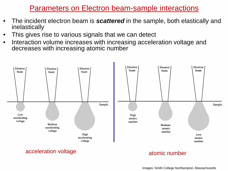
Parameters on Electron beam-sample interactions • The incident electron beam is scattered in the sample, both elastically and
inelastically • This gives rise to various signals that we can detect • Interaction volume increases with increasing acceleration voltage and
decreases with increasing atomic number
Images: Smith College Northampton, Massachusetts
acceleration voltage atomic number

Where does the signals come from?
• Diameter of the interaction volume is larger than the electron spot resolution is poorer than the size of the electron spot
• The electron beam follows a vertical path through the column of the microscope.
• Once it hits the sample, other electrons are ejected from the sample.
• Detectors collect the secondary or backscattered electrons, and convert them to a
signal that is sent to a viewing screen similar to the one in an ordinary television,
producing an image.

Secondary electrons (SE): - The most common imaging mode collects low energy <50eV Secondary electrons that are ejected from the k-shell of the specimen atoms by inelastic scattering interactions with beam electrons. Due to their low energy, these electrons originate within a few nanometers from the sample surface.
• Generated from the collision between the incoming electrons and the loosely bonded outer electrons
• Low energy electrons (~10-50 eV) • Only SE generated close to surface escape
(topographic information is obtained) • Number of SE is greater than the number of incoming
electrons • We differentiate between SE1 and SE2

SE1 • The secondary electrons that are
generated by the incoming electron beam as they enter the surface
• High resolution signal with a resolution which is only limited by the electron beam diameter
Incoming electrons SE2
• The secondary electrons that are generated by the backscattered electrons that have returned to the surface after several inelastic scattering events
• SE2 come from a surface area that is bigger than the spot from the incoming electrons resolution is poorer than for SE1 exclusively
Sample surface
SE 2

Factors that affect SE emission
1. Work function of the surface
2. Beam energy and beam current
• Electron yield goes through a maximum at low acc. voltage, then
decreases with increasing acc. voltage (page 283)
Incident electron energy / kV
Sec
onda
ry
elec
tron
yiel
d

3. Atomic number (Z) • More SE2 are created with increasing Z • The Z-dependence is more pronounced at lower beam energies
Image: Smith College Northampton, Massachusetts
Factors that affect SE emission
4. The local curvature of the surface (the most important factor)

Backscattered electrons (BSE) • A fraction of the incident electrons is retarded by
the electro-magnetic field of the nucleus and if
the scattering angle is greater than 180 ° the
electron can escape from the surface
• Back scattered electrons(BSE) consist of high-
energy electrons originating in the electron
beam, that are reflected or back-scattered out of
the specimen interaction volume by elastic
scattering interactions with specimen atoms.
•Since heavy elements (high atomic number)
backscatter electrons more strongly than light
elements (low atomic number), and thus appear
brighter in the image.

• High energy electrons (elastic scattering) • Fewer BSE than SE
Backscattered electrons (BSE)
Sample surface
BSE2

BSE as a function of atomic number
Image: University of Cape Town
• For phases containing more than one element, it is the average atomic number that determines the backscatter coefficient η

• Direction of the irritated surface
– more electrons will hit the BSE detector when the surface is
aligned towards the BSE detector
• Average atomic number
• When you want to study differences in atomic numbers the sample
should be as levelled as possible (sample preparation is an issue!)
Factors that affect BSE emission

BSE vs SE
Images: Greg Meeker, USGS
•SE produces higher resolution images than BSE
•
SE
BSE
• Resolution of 1 –2 nm is possible
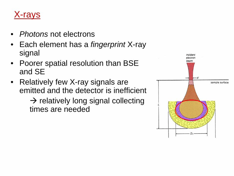
X-rays
• Photons not electrons • Each element has a fingerprint X-ray
signal • Poorer spatial resolution than BSE
and SE • Relatively few X-ray signals are
emitted and the detector is inefficient relatively long signal collecting
times are needed

X-rays
• Most common spectrometer: EDS (energy-dispersive spectrometer) • Signal overlap can be a problem • We can analyze our sample in different modes
– spot analysis – line scan – chemical concentration map (elemental mapping)

The instrument in brief

Components of the instrument • electron gun (filament) • electromagnetic optics • scan coils • sample stage • detectors • vacuum system • computer hardware and software (not trivial!!)

Electron guns: • We want many electrons per time unit per area (high current density) and
as small electron spot as possible
• Traditional guns:
– thermionic electron gun (electrons are emitted when a solid is heated)
– W-wire, LaB6-crystal
• Modern electron guns:
– field emission guns (FEG) (cold guns, a strong electric field is used to extract
electrons)
– Single crystal of W, etched to a thin tip

Electron guns:
• With field emission guns we get a smaller spot and higher current
densities compared to thermionic guns
• Vacuum requirements are tougher for a field emission guns
Single crystal of LaB6 Tungsten wire Field emission tip

Magnetic Lens System:
• Condenser lens is a lens placed right below the
electron gun and is used to adjust the width of the
electron beam as per requirement.
• The condenser lens controls the intensity of the
electron beam reaching the specimen.
• The objective lens brings the electron beam into focus
on the specimen.
• The scanning coils deflect the electron beam
horizontally and vertically over the specimen surface.
This is also called rastering.
– A fine e- beam is required for SEM, for better
performance

Specimen Stage/Chamber • It receives and supports the specimen. • Specimen stage should be able to perform the
horizontal and vertical movements smoothly. • The horizontal movement is used for selection of the
field while the vertical movement is used to change the image resolution
•The operating environment of a standard scanning electron microscope dictates that special preparation techniques are used. • Typically, a biological specimen is chemically fixed, dehydrated through an acetone or ethanol series and then dried at the critical point ‐ a method used to minimize specimen distortion due to drying tensions. • For dry samples, this process is not necessary. • SEM can also be used to investigate smooth surfaces of industrial samples. • The samples are mounted on a stub of metal with adhesive, coated with 40 ‐ 60 nm of metal such as Gold/Palladium and then observed in the microscope.

Traditional detectors
Detectors:
Secondary electron detector: (Everhart-Thornley)
Backscattered electron detector: (Solid-State Detector)
• Secondary electrons: Everhart-Thornley Detector • Backscattered electrons: Solid State Detector • X-rays: Energy dispersive spectrometer (EDS)
electron trajectories

The secondary electron detector: Everhart-Thornley detector:
The detector consists primarily of a scintillator inside a Faraday cage. A low positive voltage is applied to the Faraday cage to attract the relatively low energy (less than 50 eV by definition) secondary electrons.
Other electrons within the specimen chamber are not attracted by this low voltage and will only reach the detector if their direction of travel takes them to it. The scintillator has a high positive voltage (in the nature of 10,000 eV) to accelerate the incoming electrons to it where they can be converted to light photons. The direction of their travel is focused to the lightguide by a metal coating on the scintillator acting as a mirror. In the light pipe the photons travel outside of the microscope's vacuum chamber to a photomultiplier tube for amplification.

The BSE detector :solid state semiconductor diode
The resulting image has greyscales based on the contrast produced by the sample. The contrast of the image depends on various factors like the atomic number (Z) of the sample material, the acceleration voltage of the primary beam, and the specimen angle (tilt) with relation to the primary beam. Backscattered electrons therefore give us useful information about the composition and surface topography of the sample. Material with a high atomic number (Z), like gold (Au) will generate more BSEs than material with a lower atomic number, like silicon (Si). Because of these differences in backscatter electron yield the detector can be used to identify different phases or inclusions.
The backscattered electron detector is usually a solid state semiconductor diode operating on the principle of electron-hole production induced by energetic electrons. It has the form of a flat, thin plate with an annular opening in the middle. Solid state BSE detectors are positioned between the sample and the objective lens. The electron beam passes through a hole in the centre of the detector and backscattered electrons are collected as they are returned from the sample.
a b
BSE
SE

How do we get an image?
• In brief: we shoot high-energy electrons and analyze the outcoming electrons/x-rays
Electrons in Electrons out
or: x-rays out

How do we get an image?
156 electrons!
Image
Detector
Electron gun 288 electrons!

Why do we need vacuum?
• Chemical (corrosion!!) and thermal stability is necessary for a well-
functioning filament (gun pressure)
– A field emission gun requires ~ 10-10 Torr
– LaB6: ~ 10-6 Torr
• The signal electrons must travel from the sample to the detector
(chamber pressure)
– Vacuum requirements is dependant of the type of detector
Environmental SEM: ESEM
• Traditional SEM chamber pressure: ~ 10-6 Torr
– ESEM: 0.08 – 30 Torr
• Various gases can be used
• Requires different SE detector

Why ESEM?
• To image challenging samples such as: – insulating samples – vacuum-sensitive samples (e.g. biological samples) – irradiation-sensitive samples (e.g. thin organic films) – “wet” samples (oily, dirty, greasy)
• To study and image chemical and physical processes in-situ such
as: – mechanical stress-testing – oxidation of metals – hydration/dehydration (e.g. watching paint dry)

Some comments on resolution;
• Best resolution that can be obtained dependsa on the size of the electron spot on the sample surface
• The introduction of FEG has dramatically improved the resolution of SEM’s • The volume from which the signal electrons are formed defines the resolution
– SE image has higher resolution than a BSE image • Scanning speed:
– a weak signal requires slow speed to improve signal-to-noise ratio – when doing a slow scan drift in the electron beam can affect the accuracy of
the analysis

Summary: • The scanning electron microscope is a versatile instrument that can be
used for many purposes and can be equipped with various accessories • An electron probe is scanned across the surface of the sample and
detectors interpret the signal as a function of time • A resolution of 1 – 2 nm can be obtained when operated in a high
resolution setup • The introduction of ESEM and the field emission gun have simplified
the imaging of challenging samples

Summary
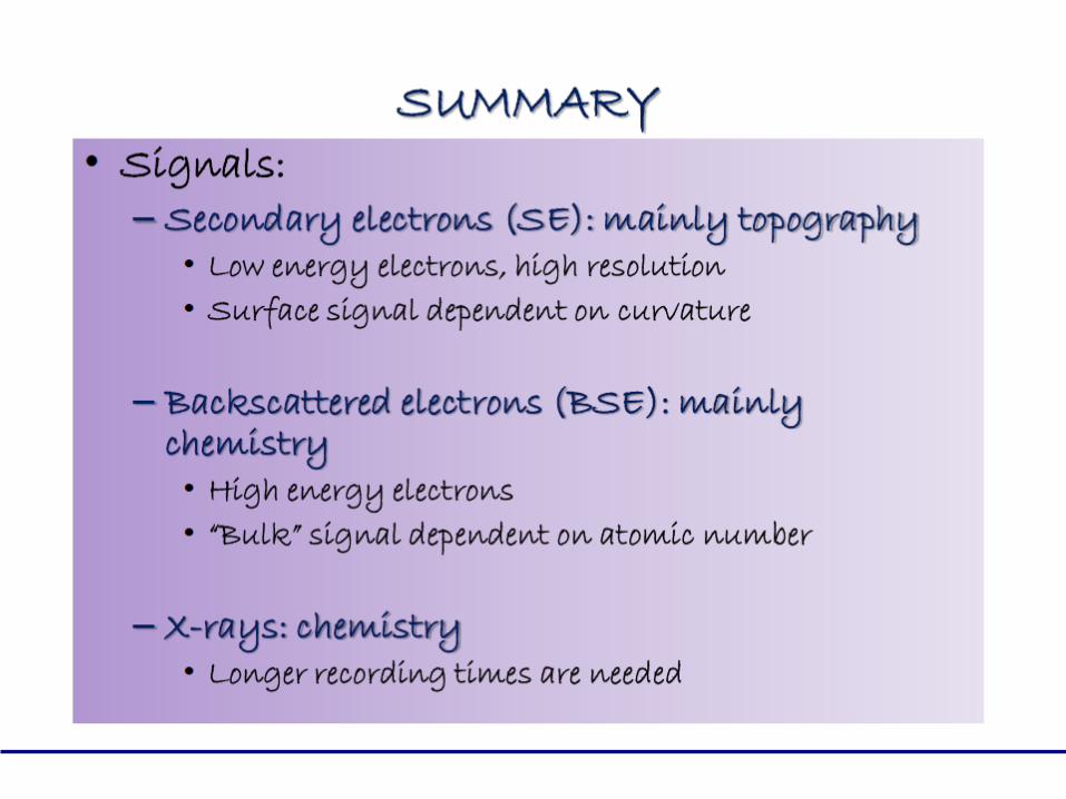
• Signals: – Secondary electrons (SE): mainly topography
• Low energy electrons, high resolution • Surface signal dependent on curvature
– Backscattered electrons (BSE): mainly chemistry • High energy electrons • “Bulk” signal dependent on atomic number
– X-rays: chemistry • Longer recording times are needed

Recommended