Shilong Pan ([email protected]), Dan Zhu ([email protected]), and Shifeng Liu ([email protected]) are with the Key Laboratory of Radar Imaging and Microwave Photonics, Ministry of Education, Nanjing University of Aeronautics and Astronautics, China. Kun Xu ([email protected]) and Yitang Dai ([email protected]) are with the State Key Laboratory of Information Photonics and Optical Communications, Beijing
University of Posts and Telecommunications, China. Tianliang Wang ([email protected]) is with the Shanghai Institute of Satellite Engineering, China. Jianguo Liu ([email protected]) and Ninghua Zhu ([email protected]) are with the State Key Laboratory on Integrated
Optoelectronics, Institution of Semiconductors, Chinese Academy of Sciences, Beijing, China. Yong Xue ([email protected]) and Naijin Liu ([email protected]) are with the Institute of Telecommunication Satellites, China Academy of Space Technology, China.
Satellite communication offers a number of distinct features that are not readily avail-able with other means of communication, such as seamless coverage of remote and sparsely populated areas, reliable data relay
for deep-space exploration, inherent multicasting and broadcasting capabilities, and reliable performance in
extreme conditions (e.g., war, earthquakes, and other adverse events) [1], [2]. In recent years, the steep rise in mobile multimedia applications and increased space exploration activity have created unprecedented op-portunities for innovative satellite communication. Ac-cording to a report provided by the Satellite Industry Association in September 2014, the global revenue of
Shilong Pan, Dan Zhu, Shifeng Liu, Kun Xu, Yitang Dai, Tianliang Wang, Jianguo Liu, Ninghua Zhu, Yong Xue, and Naijin Liu
Satellite Payloads Pay Off
FOCUSED
ISSUE FEATURE
©iim
ag
e l
iCe
NS
eD
BY
iNg
Ra
m P
UB
liS
HiN
g
Digital Object Identifier 10.1109/MMM.2015.2441619Date of publication: 7 August 2015
September 2015 611527-3342/15©2015IEEE
62 September 2015
the satellite communication industry for 2013 reached US$189.2 billion—60% of global space revenue and 4% of global telecommunications revenue [3]. Apple, Google, Amazon, Facebook, and many other large technology companies are currently seeking to bolster their satellite communication systems in the next five to ten years, fostering a continuous increase of revenue in this area.
To facilitate the rapid growth of satellite communi-cation, innovations are urgently required, specifically regarding satellite payloads. Previously, only two (or, technically, three; the third is a hybrid of the main two) types of communication satellite payloads were available: the transparent “bent-pipe” payload and the regenerative payload. The bent-pipe payload sim-ply acts as a relay to send whatever is received back to Earth solely by amplification and a shift from uplink to downlink frequency. This kind of payload is flex-ible and depends little on the physical layer, which can accommodate different multiple-access schemes, pro-tocols, and waveforms. The capacity of this type of sat-ellite is limited, however, by its bandwidth-utilization inefficiency and relatively poor bit-error-rate perfor-mance. The regenerative payload overcomes these two problems by demodulating received signals, perform-ing onboard resource allocation, and remodulating the signals for transmission back to Earth. Despite its high capacity, a regenerative payload has notable disadvan-tages in terms of its flexibility, due to intrinsic rigidity in the physical-layer interface.
Given that a communication satellite has a lifetime of 15 years or more and that the telecommunication market and technical standards have evolved so rap-idly, most satellite manufacturers and operators can only accept flexible or reconfigurable satellite pay-loads. To realize both high capacity and high flexibil-ity, a new class of payload called “software-defined payload” became, at one point, the next evolutionary step in the progress of communication satellite sys-tems. Pioneered and developed by Angeletti et al. [4] and Morlet et al. [5], a software-defined payload con-sists of a reconfigurable baseband [or intermediate frequency (IF) band] digital signal processor and a broadband analog RF platform that allow full in-orbit reconfigurability of functionalities and system param-eters according to the task at hand. This demands that the RF components, analog-to-digital converters
(ADCs), and digital-to-analog converters (DACs) in the payload have sufficient dynamic range and bandwidth covering all frequencies of the designed communica-tion tasks. Considering that the operation frequency of the satellite must move from low-frequency C/Ku bands (4–8/12–18 GHz) to high-frequency Ka (26.5–40 GHz) or Q/V bands (40–50/50–75 GHz) [6], [7], traditional electronic solutions that realize a software-defined payload inevitably face a number of critical issues, such as electromagnetic interference (EMI), mass, volume, complexity, RF isolation, and power-consumption problems.
In an effort to remedy these, there is a consensus among academics, government bodies, and industry that microwave photonic components and subsystems can replace or complement their electronic counter-parts with a net improvement in functionality, band-width, size, complexity, and cost [8]–[10], facilitating innovative implementation of communication satellite payloads [11]–[16] due to the broad bandwidth, low loss, light weight, flat frequency response, favorable isolation, and immunity to EMI provided by photonic technologies. Beginning in the early 1990s, the Euro-pean Space Agency (ESA) has supported research on microwave photonics for communication satellites. NASA, the European Seventh Framework Program, and the China Academy of Space Technology have also supported a great deal of research in the past two decades to develop novel communication satellite pay-loads based on microwave photonics. It is worth men-tioning that the efforts of the ESA in this area have led to the deployment of fiber-optic links (both digital and analog) in the Soil Moisture and Ocean Salinity obser-vation satellite launched in 2009 [17].
This article reviews the microwave photonic tech-niques developed in recent years in terms of their ability to provide a wideband or reconfigurable hardware plat-form for software-defined satellite payloads. We also discuss the challenges inherent to implementing pho-tonic components and subsystems to meet the specific requirements of software-defined satellite payloads.
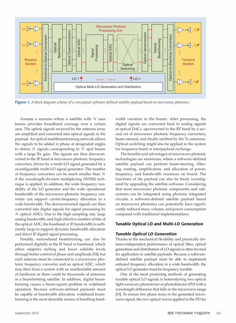
Software-Defined Payloads Based on Microwave PhotonicsFigure 1 shows the functional block scheme of a con-ceptual software-defined satellite payload based on microwave photonics. Although traditional RF amplification chains are still applied in the receive (Rx) and transmit (Tx) sections, microwave photonic components and subsystems are introduced to realize multiple-local-oscillator (LO) generation and distri-bution, frequency conversion, ADC, DAC, switching, and multibeamforming functions, making the pay-load capable of implementing high-efficiency onboard parallel signal processing with enhanced capacity while significantly reducing mass, volume, and power consumption.
According to a report provided by the Satellite Industry Association in September 2014, the global revenue of the satellite communication industry for 2013 reached US$189.2 billion.
September 2015 63
Assume a scenario where a satellite with N user beams provides broadband coverage over a certain area. The uplink signals received by the antenna array are amplified and converted into optical signals in the payload. An optical multibeamforming network allows the signals to be added in phase at designated angles to obtain N signals corresponding to N spot beams with a large Rx gain. The signals are then downcon-verted to the IF band at microwave photonic frequency converters driven by a multi-LO signal generated by a reconfigurable multi-LO signal generator. The number of frequency converters can be much smaller than N if the wavelength-division multiplexing (WDM) tech-nique is applied. In addition, the wide frequency tun-ability of the LO generator and the wide operational bandwidth of the microwave photonic frequency con-verter can support carrier-frequency allocation in a wide bandwidth. The downconverted signals are then converted into digital signals for signal processing by N optical ADCs. Due to the high sampling rate, large analog bandwidth, and high effective number of bits of the optical ADC, the baseband or IF bandwidth is suffi-ciently large to support dynamic bandwidth allocation and direct IF digital signal processing.
Notably, narrowband beamforming can also be performed digitally at the IF band or baseband, which offers adaptive nulling and lower sidelobe levels through better control of phase and amplitude [18]; but each antenna must be connected to a microwave pho-tonic frequency converter and an optical ADC, which may then form a system with an unaffordable amount of hardware as there could be thousands of antennas in a beamforming satellite. In addition, digital beam-forming causes a beam-squint problem in wideband operation. Because software-defined payloads must be capable of bandwidth allocation, wideband beam-forming is the most desirable means of handling band-
width variation in the beams. After processing, the digital signals are converted back to analog signals at optical DACs, upconverted to the RF band by a sec-ond set of microwave photonic frequency converters, beam-steered, and finally emitted by the Tx antennas. Optical switching might also be applied in the system for frequency-band or interpayload exchange.
The benefits and advantages of microwave photonic technologies are numerous, where a software-defined satellite payload can perform beam-steering, filter-ing, routing, amplification, and allocation of power, frequency, and bandwidth resources on board. The functions of the payload can also be freely reconfig-ured by upgrading the satellite software. Considering that most microwave photonic components and sub-systems can be integrated using photonic integrated circuits, a software-defined satellite payload based on microwave photonics can potentially have signifi-cantly reduced mass, volume, and power consumption compared with traditional implementations.
Tunable Optical LO and Multi-LO Generation
Tunable Optical LO GenerationThanks to the mechanical flexibility and practically dis-tance-independent performance of optical fiber, optical generation and distribution of LO signals is often favored for application in satellite payloads. Because a software-defined satellite payload must be able to implement onboard frequency allocation in a wide bandwidth, the optical LO generator must be frequency tunable.
One of the most promising methods of generating tunable optical LO signals is heterodyning two optical light waves at a photomixer or photodetector (PD) with a wavelength difference that falls in the microwave range [19]. To ensure low phase noise in the generated micro-wave signal, the two optical waves applied to the PD for
Microwave PhotonicProcessing Unit
ReceiveSection
TransmitSection
Ele
ctric
al-t
o-O
ptic
al C
onve
rsio
n
Opt
ical
AD
C
Opt
ical
Dow
ncon
vers
ion
Opt
ical
Bea
mfo
rmin
g
Opt
ical
-to-
Ele
ctric
al C
onve
rsio
n
Sig
nal
Pro
cess
ing
Opt
ical
Bea
mfo
rmin
g
Opt
ical
DA
C
Opt
ical
Upc
onve
rsio
n
OpticalSwitching
Optical Multi-LO Generation and Distribution
LO 1 LO n
Figure 1. A block diagram scheme of a conceptual software-defined satellite payload based on microwave photonics.
64 September 2015
heterodyning must be phase correlated. A simple and cost-effective way of producing two optical waves is to employ a dual-wavelength, single-longitudinal-mode laser source [20], [21], but the phase correlation between the two wavelengths is generally not good enough to generate an LO signal with acceptable phase-noise level. A phase-locked loop (PLL) is thus required to lock the phase of one wavelength onto the other, which further requires a low-noise microwave reference with the same frequency as that of the generated LO signal [21].
Two phase-correlated optical waves can also be gen-erated by optical frequency multiplication based on electro-optical modulators [22], [23]. Although a high-quality reference is still required, the frequency can be much lower because the maximal achievable frequency multiplication factor can be larger than 25 [23]. It should be noted that the larger multiplication factor requires higher-order nonlinearity in the electro-optical modu-lator, which drives down power efficiency, raises com-plexity, and degrades spectral purity. To this end, for the microwave photonic satellite payload demonstrator described in the ESA project titled “Optical Handling of Microwave and Digital Signals,” Aveline et al. [24] applied only optical double-sideband modulation with carrier suppression to generate a frequency-doubled optical LO with high power.
In addition to optical heterodyne approaches, the optoelectronic oscillator (OEO) system, invented by Yao and Maleki [25], also shows promising application to high-quality optical LO signals. Due to the extremely low loss in the optical fiber delay line incorporated in the oscillation loop, a cavity with a very high Q fac-tor can be created. The Q factor of the OEO cavity can easily reach the 106 level, significantly reducing phase noise in the generated microwave signal. In a study on OEOs [26], a 10-GHz signal with a recorded phase noise of -163 dBc/Hz at 6-kHz offset was generated. It is important to note that the phase noise of the OEO is independent of the oscillation frequency, so the phase noise performance of the OEO does not degrade at higher frequencies [25].
The OEO can be very compact if an ultrahigh-Q whispering-gallery-mode resonator is used to replace the long fiber. Remarkably, an ultracompact OEO pack-age smaller than a coin was reported previously [27], as was a miniature 35-GHz OEO with a phase noise of -108 dBc/Hz at 10-kHz offset and a form factor of 0.5 # 0.5 # 0.25 in [28], demonstrating the significant potential of OEOs for deployment in satellite payloads.
If a flexible microwave photonic filter is incorpo-rated in the oscillation loop, the OEO can be made frequency tunable. For example, an OEO incorpo-rated with a high-Q microwave photonic filter based on an externally injected Fabry–Pérot laser diode (LD) can generate an LO signal that is frequency tun-able from 6.41 to 10.85 GHz [29]. A microwave pho-tonic filter based on polarization modulation and
dispersive elements also enabled a tuning range of 5.8–11.8 GHz in [30]. More recently, Peng et al. [31] have reported an OEO with a recorded tuning range of 60 GHz based on stimulated Brillouin scattering.
Multi-LO GenerationFor communication satellites with multibeam broad-band access capability, multi-LO signal generation is also essential. For instance, in an ESA project titled “Optical Wideband–Reconfigurable Receiver Front-End,” at least 13 LOs were required in the payload to achieve multi-beam broadband satellite coverage over Europe [24]. Sev-eral schemes to realize photonic generation of multi-LO signals have been proposed.
A typical multi-LO generator was realized in [32] using two optical frequency combs (OFCs), with the free spectral ranges of each in a frequency difference of
.fD If the zeroth-order comb lines of the two OFCs are of the same frequency, the nth-order comb lines have a frequency difference of .n fD After beating at a PD, a multi-LO signal with a frequency spacing of fD can be generated. In addition, a reconfigurable optical filter can be inserted before the PD to select the designated channels. A key drawback of this method, however, is that the optical energy efficiency is very low, and the resulting signal quality is quite poor. Also, because the two OFCs are generated by two independent systems, a PLL circuit is required to phase lock the two OFCs.
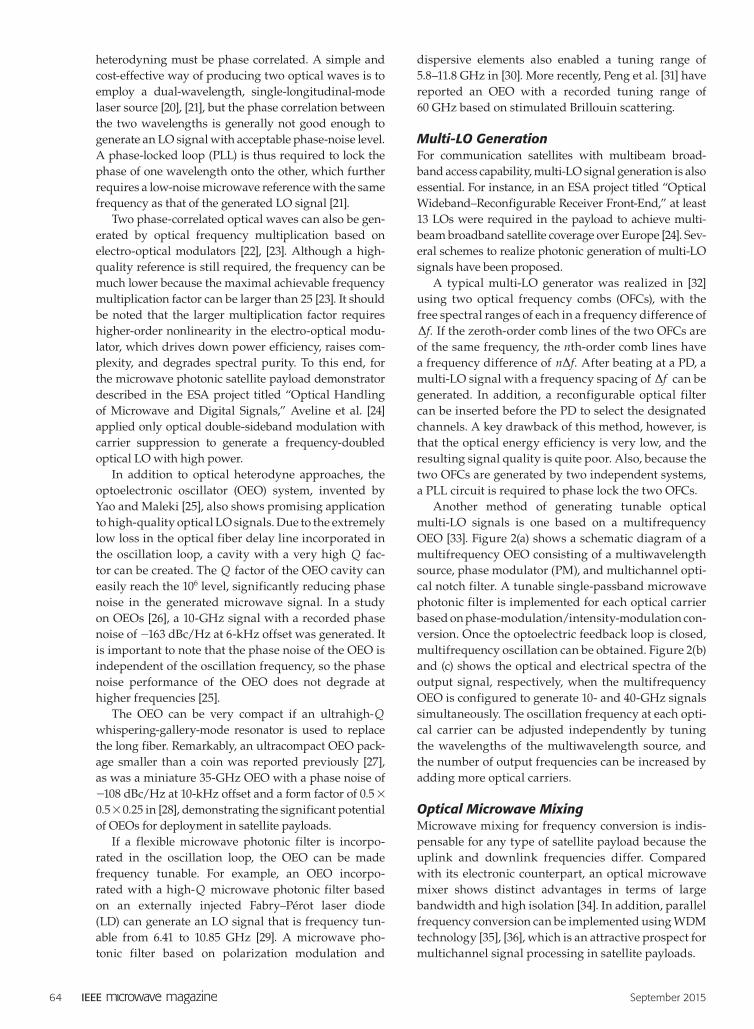
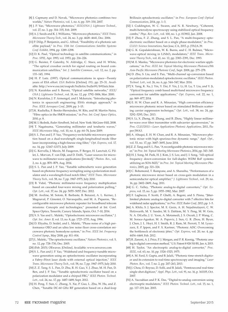
Another method of generating tunable optical multi-LO signals is one based on a multifrequency OEO [33]. Figure 2(a) shows a schematic diagram of a multifrequency OEO consisting of a multiwavelength source, phase modulator (PM), and multichannel opti-cal notch filter. A tunable single-passband microwave photonic filter is implemented for each optical carrier based on phase-modulation/intensity-modulation con-version. Once the optoelectric feedback loop is closed, multifrequency oscillation can be obtained. Figure 2(b) and (c) shows the optical and electrical spectra of the output signal, respectively, when the multifrequency OEO is configured to generate 10- and 40-GHz signals simultaneously. The oscillation frequency at each opti-cal carrier can be adjusted independently by tuning the wavelengths of the multiwavelength source, and the number of output frequencies can be increased by adding more optical carriers.
Optical Microwave MixingMicrowave mixing for frequency conversion is indis-pensable for any type of satellite payload because the uplink and downlink frequencies differ. Compared with its electronic counterpart, an optical microwave mixer shows distinct advantages in terms of large bandwidth and high isolation [34]. In addition, parallel frequency conversion can be implemented using WDM technology [35], [36], which is an attractive prospect for multichannel signal processing in satellite payloads.
September 2015 65
The most common method of implementing optical microwave mixing (the one adopted by the ESA micro-wave photonic payload demonstrator [16]) is simply a Mach–Zehnder modulator (MZM), in which the opti-cal LO signal and the driven RF signal are multiplied via the Pockels electro-optic effect in the MZM. If multiple optical LO signals are sent to the MZM, all LOs are combined with the RF signal to generate mul-tiple IF signals at the same time. For example, taking advantage of the optical LOs generated by the OFC, a 6.1-GHz C-Band signal can be converted to 4.1-GHz (C Band), 3.9-GHz (C Band), and 11.9-GHz (X Band) signals simultaneously [37]. Due to the negligible opti-cal nonlinearity in the MZM and the optical fiber, optical LOs and IFs with different wavelengths do not interact, so large channel isolation can be guaranteed.
Necessary improvements to MZM-based optical mixing performance include enhancing conversion efficiency, linearity, and functionality; previous studies have proposed several innovative optical microwave solutions to do so. For example, to improve conversion efficiency, optical amplification was applied, result-ing in an improvement as large as 26 dB [38]. Linear-ity, which can be characterized by a parameter called spurious free dynamic range (SFDR), is also a very important parameter for optical microwave mixers. To date, the reported highest SFDRs for an optical micro-wave mixer are 122.72/3 dB$Hz (considering the third intermodulation distortion) and 127 4/5 dB$Hz (consid-ering the fifth intermodulation distortion), realized by a linearized dual-parallel MZM [39], [40]. The majority of the optical microwave mixers reported in previous studies only achieved the simplest likely single-ended frequency mixing.
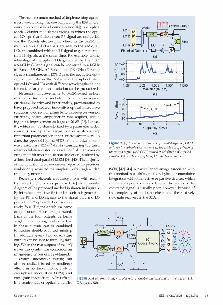
Recently, a photonic frequency mixer with recon-figurable functions was proposed [41]. A schematic diagram of the proposed method is shown in Figure 3. By introducing the two first-order sidebands generated by the RF and LO signals to the signal port and LO port of a 90° optical hybrid, respec-tively, four IF signals with the same or quadrature phases are generated. Each of the four outputs performs single-ended mixing, and every two in-phase outputs can be combined to realize double-balanced mixing. In addition, every two quadrature outputs can be used to form I/Q mix-ing. When the two outputs of the I/Q mixer are quadrature combined, an image-reject mixer can be obtained.
Optical microwave mixing can also be realized based on nonlinear effects in nonlinear media, such as cross-phase modulation (XPM) and cross-gain modulation (XGM) effects in a semiconductor optical amplifier
(SOA) [42], [43]. A particular advantage associated with this method is its ability to allow hybrid or monolithic integration with other active or passive devices, which can reduce system cost considerably. The quality of the converted signal is usually poor, however, because of the complexity of nonlinear effects and the relatively slow gain recovery in the SOA.
Pow
er (
dBm
)
1,551 1,552 1,553 1,554 1,555
-80
-60
-40
-20
Wavelength (nm)
0 10 20 30 40
-80
-60
-40
-20
0
Pow
er (
dBm
)
Frequency (GHz)
(b)
(c)
(a)
10 GHz 40 GHz
LD 1
PDEAEC
PMLD 2
Electrical Output
WDM
LD n
OC
Optical Output
Fiber
… ……
ONF
Figure 2. (a) A schematic diagram of a multifrequency OEO, with (b) the optical spectrum and (c) the electrical spectrum of the output signal [33]. ONF: optical notch filter; OC: optical coupler; EA: electrical amplifier; EC: electrical coupler.
RF
LO
OF1
OF2
iI1
iI2iQ1
iQ2LO
Signal
I1
Q2
I2Q1
90°Optical Hybrid
~RF
~LO
PD Array
LD
MZM1
MZM2
Figure 3. A schematic diagram of a reconfigurable photonic microwave mixer [41]. OF: optical filter.
66 September 2015
Optical Analog-to-Digital ConversionThe device in a software-defined payload that connects the RF receiver and the digital processor is the ADC. An ADC with fast sampling rate, large analog bandwidth, and high effective number of bits (ENOB) is most desir-able for any software-defined system; however, any aperture error in an electronic ADC degrades the sig-nal-to-noise/distortion ratio at high input frequencies [44], resulting in a tradeoff between the analog band-width and the ENOB. In addition, the sampling rate of electronic ADCs is limited by comparator ambiguity. It is thus rather difficult for even state-of-the-art electronic ADCs to realize large analog bandwidth, large ENOB, and high sampling rate simultaneously.
Due to the large bandwidth, ultralow-timing jitter-pulse-generation capability, and EMI immunity of
modern photonics, many microwave photonic tech-niques have been developed to realize sampling [45]–[47], digitization [48], or signal stretching [49], [50] in the past few decades. Photonic-assisted electronic ADCs are often called “optical ADCs,” although the analog signal to be converted is an electrical signal rather than an optical signal.
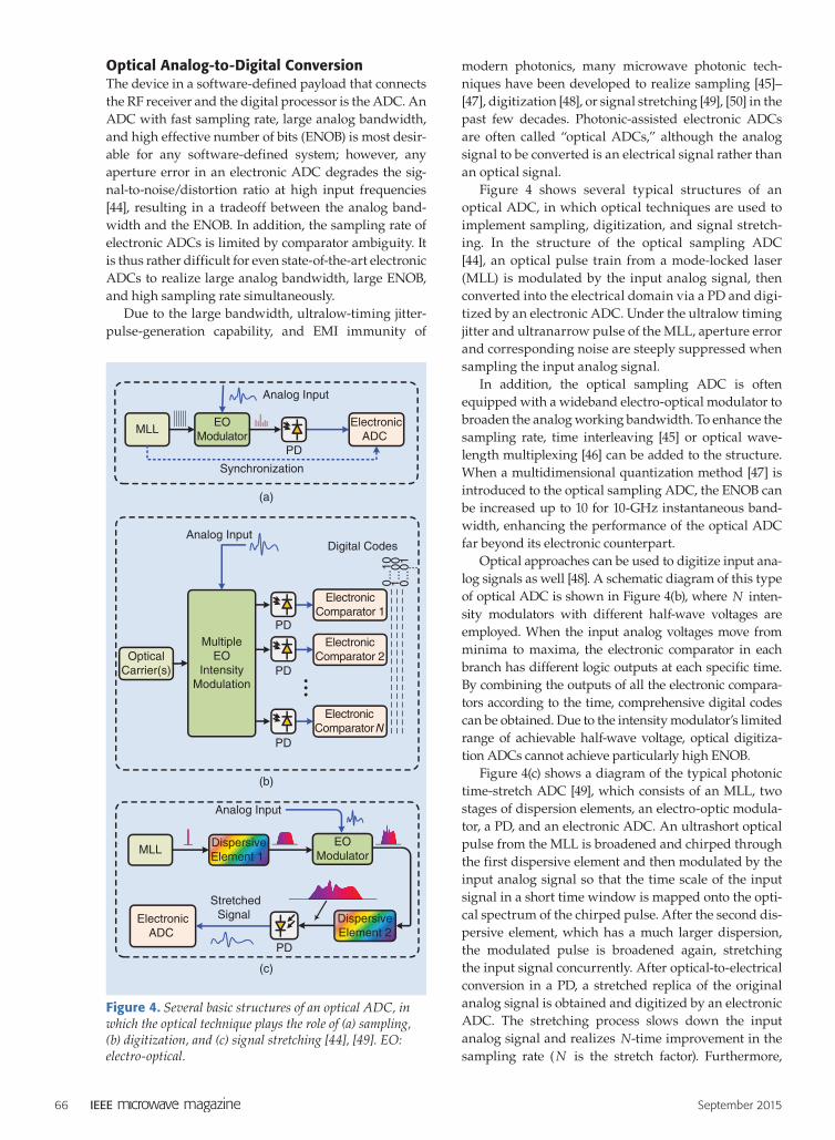
Figure 4 shows several typical structures of an optical ADC, in which optical techniques are used to implement sampling, digitization, and signal stretch-ing. In the structure of the optical sampling ADC [44], an optical pulse train from a mode-locked laser (MLL) is modulated by the input analog signal, then converted into the electrical domain via a PD and digi-tized by an electronic ADC. Under the ultralow timing jitter and ultranarrow pulse of the MLL, aperture error and corresponding noise are steeply suppressed when sampling the input analog signal.
In addition, the optical sampling ADC is often equipped with a wideband electro-optical modulator to broaden the analog working bandwidth. To enhance the sampling rate, time interleaving [45] or optical wave-length multiplexing [46] can be added to the structure. When a multidimensional quantization method [47] is introduced to the optical sampling ADC, the ENOB can be increased up to 10 for 10-GHz instantaneous band-width, enhancing the performance of the optical ADC far beyond its electronic counterpart.
Optical approaches can be used to digitize input ana-log signals as well [48]. A schematic diagram of this type of optical ADC is shown in Figure 4(b), where N inten-sity modulators with different half-wave voltages are employed. When the input analog voltages move from minima to maxima, the electronic comparator in each branch has different logic outputs at each specific time. By combining the outputs of all the electronic compara-tors according to the time, comprehensive digital codes can be obtained. Due to the intensity modulator’s limited range of achievable half-wave voltage, optical digitiza-tion ADCs cannot achieve particularly high ENOB.
Figure 4(c) shows a diagram of the typical photonic time-stretch ADC [49], which consists of an MLL, two stages of dispersion elements, an electro-optic modula-tor, a PD, and an electronic ADC. An ultrashort optical pulse from the MLL is broadened and chirped through the first dispersive element and then modulated by the input analog signal so that the time scale of the input signal in a short time window is mapped onto the opti-cal spectrum of the chirped pulse. After the second dis-persive element, which has a much larger dispersion, the modulated pulse is broadened again, stretching the input signal concurrently. After optical-to-electrical conversion in a PD, a stretched replica of the original analog signal is obtained and digitized by an electronic ADC. The stretching process slows down the input analog signal and realizes N-time improvement in the sampling rate (N is the stretch factor). Furthermore,
Analog Input
Analog Input
Synchronization
PD
PD
PD
PD
PD
MLL
MLL
(a)
(b)
(c)
EOModulator
EOModulator
ElectronicADC
ElectronicADC
MultipleEO
IntensityModulation
ElectronicComparator 1
ElectronicComparator 2
ElectronicComparatorN
Digital Codes
0...1
01.
..00
0...0
1...
OpticalCarrier(s)
DispersiveElement 1
DispersiveElement 2
StretchedSignal
Analog Input
Figure 4. Several basic structures of an optical ADC, in which the optical technique plays the role of (a) sampling, (b) digitization, and (c) signal stretching [44], [49]. EO: electro-optical.
September 2015 67
the bandwidth of the input signal is compressed, which increases the equivalent analog bandwidth and reduces any noise due to aperture error. Using distrib-uted Raman optical amplification, 10 TSa/s equivalent sampling was demonstrated in a previous study with a stretch factor up to 250 [50]. In addition, since most pho-tonic ADCs have electronic ADCs as the back ends, the performance of the photonic ADC will also be improved with the rapid development of electronic ADC.
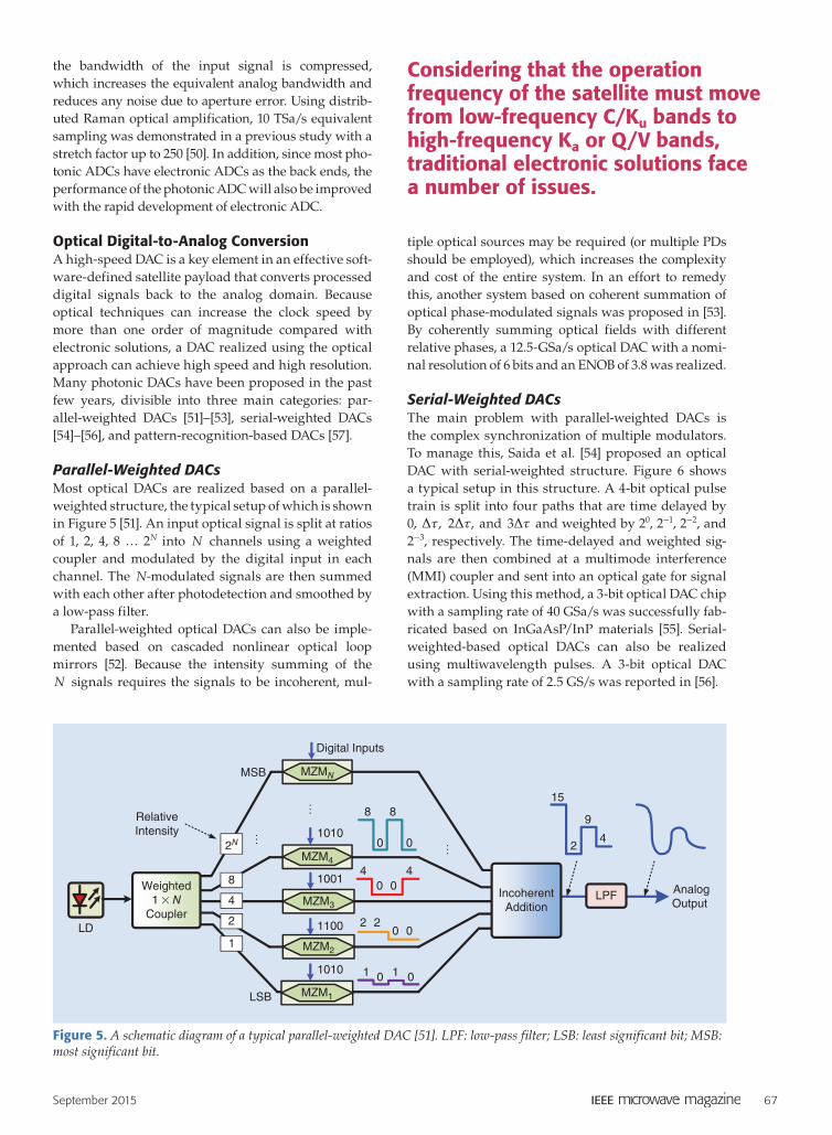
Optical Digital-to-Analog ConversionA high-speed DAC is a key element in an effective soft-ware-defined satellite payload that converts processed digital signals back to the analog domain. Because optical techniques can increase the clock speed by more than one order of magnitude compared with electronic solutions, a DAC realized using the optical approach can achieve high speed and high resolution. Many photonic DACs have been proposed in the past few years, divisible into three main categories: par-allel-weighted DACs [51]–[53], serial-weighted DACs [54]–[56], and pattern-recognition-based DACs [57].
Parallel-Weighted DACsMost optical DACs are realized based on a parallel-weighted structure, the typical setup of which is shown in Figure 5 [51]. An input optical signal is split at ratios of 1, 2, 4, 8 … 2N into N channels using a weighted coupler and modulated by the digital input in each channel. The N-modulated signals are then summed with each other after photodetection and smoothed by a low-pass filter.
Parallel-weighted optical DACs can also be imple-mented based on cascaded nonlinear optical loop mirrors [52]. Because the intensity summing of the N signals requires the signals to be incoherent, mul-
tiple optical sources may be required (or multiple PDs should be employed), which increases the complexity and cost of the entire system. In an effort to remedy this, another system based on coherent summation of optical phase-modulated signals was proposed in [53]. By coherently summing optical fields with different relative phases, a 12.5-GSa/s optical DAC with a nomi-nal resolution of 6 bits and an ENOB of 3.8 was realized.
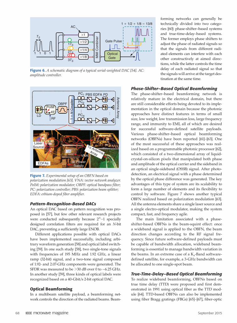
Serial-Weighted DACsThe main problem with parallel-weighted DACs is the complex synchronization of multiple modulators. To manage this, Saida et al. [54] proposed an optical DAC with serial-weighted structure. Figure 6 shows a typical setup in this structure. A 4-bit optical pulse train is split into four paths that are time delayed by 0, ,xD ,2 xD and 3 xD and weighted by 20, 2-1, 2-2, and 2-3, respectively. The time-delayed and weighted sig-nals are then combined at a multimode interference (MMI) coupler and sent into an optical gate for signal extraction. Using this method, a 3-bit optical DAC chip with a sampling rate of 40 GSa/s was successfully fab-ricated based on InGaAsP/InP materials [55]. Serial-weighted-based optical DACs can also be realized using multiwavelength pulses. A 3-bit optical DAC with a sampling rate of 2.5 GS/s was reported in [56].
LD
Weighted1 # N
Coupler
RelativeIntensity
LSB
Digital Inputs
1010
1001
1100
1010
2N
8
4
2
1
MSB
h
hh
MZM1
MZM2
MZM3
MZM4
MZMN
8 8
0 0
0 0
0 0
0 0
4 4
2 2
1 1
IncoherentAddition
AnalogOutput
15
42
9
LPF
Figure 5. A schematic diagram of a typical parallel-weighted DAC [51]. LPF: low-pass filter; LSB: least significant bit; MSB: most significant bit.
Considering that the operation frequency of the satellite must move from low-frequency C/Ku bands to high-frequency Ka or Q/V bands, traditional electronic solutions face a number of issues.
68 September 2015
Pattern-Recognition-Based DACsAn optical DAC based on pattern recognition was pro-posed in [57], but few other relevant research projects were conducted subsequently because 2N-1 specially designed correlation filters are required for an N-bit DAC, preventing a sufficiently large ENOB.
Different applications possible with optical DACs have been implemented successfully, including arbi-trary waveform generation [58] and optical label switch-ing [59]. In one such study [58], two single-tone signals with frequencies of 195 MHz and 1.92 GHz, a linear ramp (32-bit) signal, and a two-tone signal composed of 1.92- and 2.07-GHz components were generated. The SFDR was measured to be 230 dB over 0 to a6.25 GHz. In another study [59], three kinds of optical labels were recognized based on a 40-Gbit/s 2-bit optical DAC.
Optical BeamformingIn a multibeam satellite payload, a beamforming net-work controls the direction of the radiated beams. Beam-
forming networks can generally be technically divided into two catego-ries [60]: phase-shifter–based systems and true-time-delay–based systems. The former employs phase shifters to adjust the phase of radiated signals so that the signals from different radi-ated elements can interfere with each other constructively at aimed direc-tions, while the latter controls the time delay of each radiated signal so that the signals will arrive at the target des-tination at the same time.
Phase-Shifter–Based Optical BeamformingThe phase-shifter–based beamforming network is relatively mature in the electrical domain, but there are still considerable efforts being devoted to its imple-mentation in the optical domain because the photonic approaches have distinct features in terms of small size, low weight, low transmission loss, large frequency range, and immunity to EMI, all of which are desired for successful software-defined satellite payloads. Various phase-shifter–based optical beamforming networks (OBFNs) have been reported [61]–[63]. One of the most successful of these approaches was real-ized based on a programmable photonic processor [62], which consisted of a two-dimensional array of liquid-crystal-on-silicon pixels that manipulated both phase and amplitude of the optical carrier and the sideband in an optical single-sideband (OSSB) signal. After photo-detection, an electrical signal with a phase determined by the optical phase difference was generated. The key advantages of this type of system are its scalability to form a large number of elements and its flexibility to control by software. Figure 7 shows another typical OBFN realized based on polarization modulation [63]. All the antenna elements share a single laser source and a single electro-optical modulator, making the system compact, fast, and frequency agile.
The main limitation associated with a phase-shifter-based OBFNs is the beam-squint effect: once a wideband signal is applied to the OBFN, the beam direction changes according to the RF signal fre-quency. Since future software-defined payloads must be capable of bandwidth allocation, wideband beam-forming is essential to manage bandwidth variation in the beams. In an extreme case of a Ka-Band software-defined satellite, for example, a 3-GHz bandwidth can be allocated to one single-spot beam.
True-Time-Delay–Based Optical Beamforming To realize wideband beamforming, OBFNs based on true time delay (TTD) were proposed and first dem-onstrated in 1991 using optical fiber as the TTD mod-ule [64]. TTD-based OBFNs can also be implemented using fiber Bragg gratings (FBGs) [65]–[67], fiber-optic
1TS
2TS
3TS
#1
#1/2
#1/4
#1/8 MM
I Com
bine
r
OpticalGate
Gate Pulse
1 + 1/2 + 1/8 = 13/8
TS
1 1 10
AC
Figure 6. A schematic diagram of a typical serial-weighted DAC [54]. AC: amplitude controller.
LDLD
PoIM
1 #
N C
oupl
er
OBPF
RF
45°
PC1 PBS EDFA PD Antenna A
rray
PC2
…
…PCN
LaserSource
EDFAs dc PowerSupply
VNA
To AntennaArray
Figure 7. Experimental setup of an OBFN based on polarization modulation [63]. VNA: vector network analyzer. PolM: polarization modulator; OBPF: optical bandpass filter; PC: polarization controller; PBS: polarization beam splitter; EDFA: erbium-doped fiber amplifier.
September 2015 69
delay line matrices [68], [69], slow light [70], [71], and on-chip ring resonators [72], [73]. Among these, inte-grated OBFNs based on on-chip ring resonators are most attractive thanks to their ultracompact foot-print. An 8 # 1 OBFN chip [72] and a 4 # 4 OBFN chip [73] were recently fabricated with dimensions of 21 # 11 mm2 and 36 # 8 mm2, respectively. In another study, an optical delay line with a physical path length of 27 m was realized on a 9.5 # 9.5 cm2 silicon chip [74], showing potential application to the construction of a miniature TTD-based OBFN.
The physical time delay in TTD-based OBFNs intrinsically steers RF signals to a single direction regardless of frequency, but software-defined satel-lite payloads require multibeamforming to support multiple-spot beams. Subbaraman et al. [75] realized an optical TTD multibeam OBFN based on highly dispersive photonic crystal fibers; for the Tx mode and Rx mode, however, different architectures must be employed, making the system complex, inefficient, and inflexible. Another multibeam OBFN [76] was investigated using a MLL and dispersive element to steer multiple RF signals simultaneously. The main problem associated with this system was that it does not work in the Rx mode and has limited operation bandwidth.
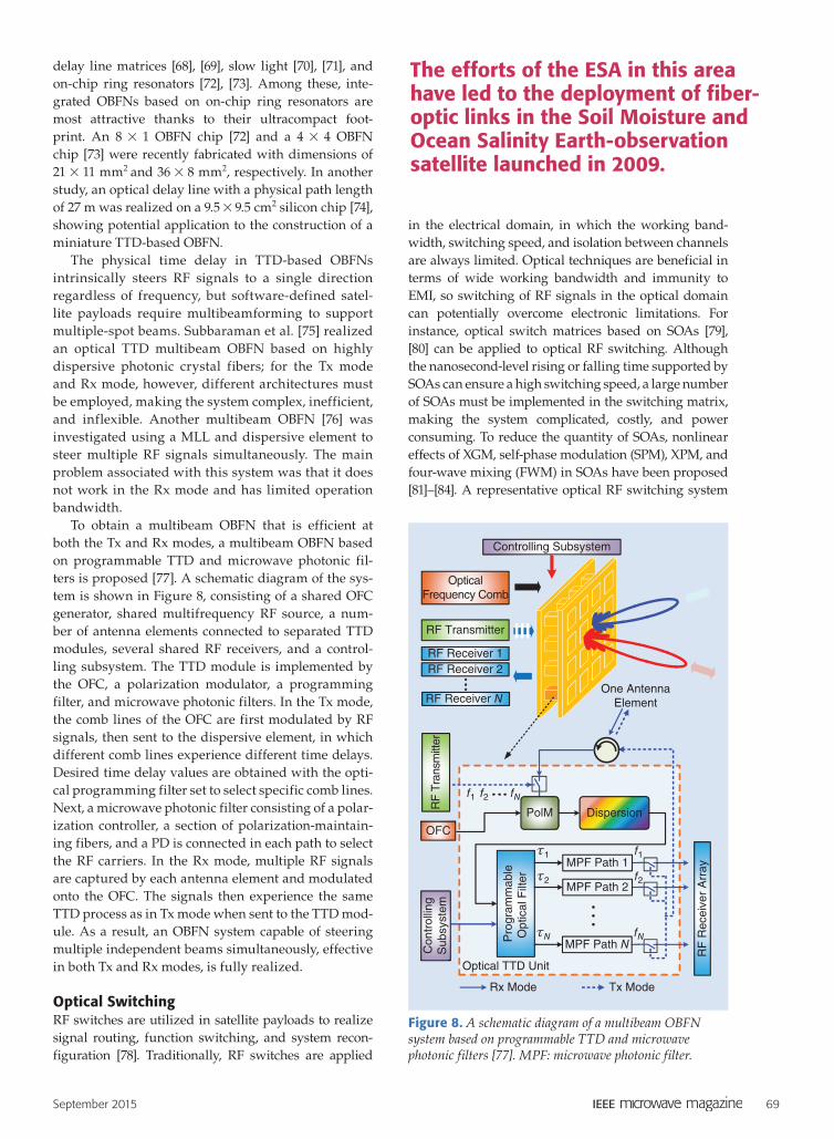
To obtain a multibeam OBFN that is efficient at both the Tx and Rx modes, a multibeam OBFN based on programmable TTD and microwave photonic fil-ters is proposed [77]. A schematic diagram of the sys-tem is shown in Figure 8, consisting of a shared OFC generator, shared multifrequency RF source, a num-ber of antenna elements connected to separated TTD modules, several shared RF receivers, and a control-ling subsystem. The TTD module is implemented by the OFC, a polarization modulator, a programming filter, and microwave photonic filters. In the Tx mode, the comb lines of the OFC are first modulated by RF signals, then sent to the dispersive element, in which different comb lines experience different time delays. Desired time delay values are obtained with the opti-cal programming filter set to select specific comb lines. Next, a microwave photonic filter consisting of a polar-ization controller, a section of polarization-maintain-ing fibers, and a PD is connected in each path to select the RF carriers. In the Rx mode, multiple RF signals are captured by each antenna element and modulated onto the OFC. The signals then experience the same TTD process as in Tx mode when sent to the TTD mod-ule. As a result, an OBFN system capable of steering multiple independent beams simultaneously, effective in both Tx and Rx modes, is fully realized.
Optical SwitchingRF switches are utilized in satellite payloads to realize signal routing, function switching, and system recon-figuration [78]. Traditionally, RF switches are applied
in the electrical domain, in which the working band-width, switching speed, and isolation between channels are always limited. Optical techniques are beneficial in terms of wide working bandwidth and immunity to EMI, so switching of RF signals in the optical domain can potentially overcome electronic limitations. For instance, optical switch matrices based on SOAs [79], [80] can be applied to optical RF switching. Although the nanosecond-level rising or falling time supported by SOAs can ensure a high switching speed, a large number of SOAs must be implemented in the switching matrix, making the system complicated, costly, and power consuming. To reduce the quantity of SOAs, nonlinear effects of XGM, self-phase modulation (SPM), XPM, and four-wave mixing (FWM) in SOAs have been proposed [81]–[84]. A representative optical RF switching system
Optical TTD Unit
OpticalFrequency Comb
Dispersion
Pro
gram
mab
leO
ptic
al F
ilter
Con
trol
ling
Sub
syst
em
RF
Rec
eive
r A
rray
RF
Tra
nsm
itter
Controlling Subsystem
One AntennaElement
Tx ModeRx Mode
MPF Path 1
PolM
RF Transmitter
RF Receiver 1RF Receiver 2
RF Receiver N
MPF Path N
MPF Path 2
OFC
fN
fN
f2
f2
f1
f1
xN
x2
x1
Figure 8. A schematic diagram of a multibeam OBFN system based on programmable TTD and microwave photonic filters [77]. MPF: microwave photonic filter.
The efforts of the ESA in this area have led to the deployment of fiber-optic links in the Soil Moisture and Ocean Salinity Earth-observation satellite launched in 2009.
70 September 2015
Ant
enna
s
Filt
er
Opt
ical
Sw
itch
2 #
2 S
atel
lite
Rep
eate
r
(a)
(b)
OE
O
PD
2
PD
3
LD
MZ
M
MZM
MZM
Vid
eo 1
Vid
eo 2
LO1
Mix
erG
roun
d T
x S
tatio
nG
roun
d R
x S
tatio
n
Mix
er
Am
p
Am
p
l 1l 2
m1
m2
Ant
enna
s
LO 2
Mon
itor
2
Mon
itor
1
Mon
itor
1M
onito
r 2
Opt
ical
Sw
itch
Ant
enna
sO
scill
osco
pe
Spe
ctru
m A
naly
ser
Vid
eo 1
Vid
eo 2
Ant
enna
sO
ptic
al S
witc
hO
scill
osco
pe
Spe
ctru
m A
naly
serM
onito
r 1
Mon
itor
2
Vid
eo 1
Vid
eo 2
Figu
re 9
. (a)
The
sch
emat
ic d
iagr
am a
nd (b
) exp
erim
enta
l dem
onst
rati
on o
f a 2
# 2
mic
row
ave
phot
onic
sw
itch
for
HD
vid
eo. A
mp:
ele
ctri
cal a
mpl
ifier
.
September 2015 71
based on SPM, XGM, and FWM effects in the SOA was proposed and demonstrated [84] in which only a single SOA was required for OSSB wavelength conversion.
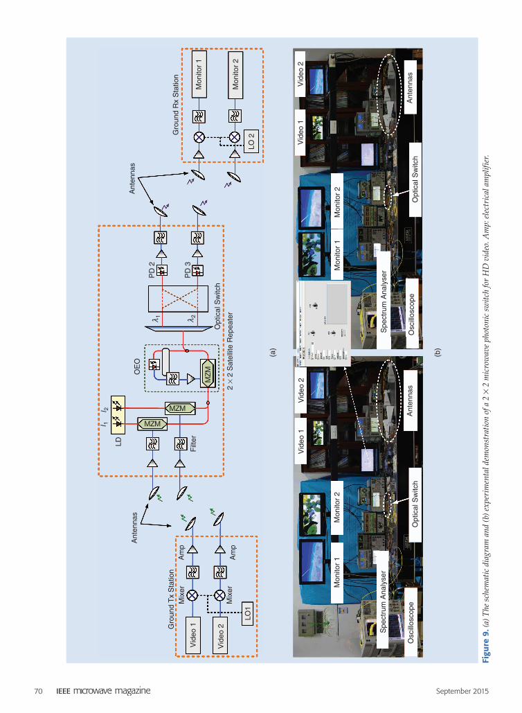
Optical RF switching can also be achieved through microelectromechanical system (MEMS) optical switches [85]. A 2 # 2 proof-of-concept microwave photonic repeater configuration using arrayed lasers, optical frequency mixers, and a MEMS optical switch was demonstrated, as shown in Figure 9, where stable switching of high-definition (HD) video signals with 1.5-GHz bandwidth was successfully realized. Two HD video signals are upconverted to Ku Band (16 GHz) and transmitted separately to the free space through two antennas, emulating two transmitters at the Earth sta-tion. In the Rx part of the microwave photonic repeater, signals from the two antennas are modulated onto two optical carriers with different wavelengths. The two optical signals are combined, simultaneously down-converted to the IF band in an OEO, and then sepa-rated by a wavelength-division demultiplexer. Optical switching of the two channels is realized by an optical MEMS switch controlled by a computer. After optical-to-electrical conversion and further downconversion, the switched signals are sent to separate monitors to verify the switching results. As shown in Figure 9(b), the video signals are on-board exchanged in the analog domain successfully by an optical MEMS switch with-out cross interference, thanks to the isolation of differ-ent optical paths in the MEMS optical switch.
Discussion and ConclusionThis article reviewed recent developments in micro-wave photonics for potential application in satel-lite payloads. By introducing microwave photonic components plus subsystems, which realize multi-LO generation and distribution, frequency conver-sion, analog-to-digital conversion, digital-to-analog conversion, multibeamforming, and switching, broadband analog RF platforms can be constructed to feasibly implement software-defined satellite payloads operated in the high-frequency band, at significantly reduced mass, volume, and power con-sumption.
Software-defined satellite payloads based on micro-wave photonics will remain purely conceptual well into the future, however, because the majority of microwave photonic techniques are still relatively unsophisticated. These components and subsystems are limited primar-ily by their inability to manage noise during electrical-to-optical or optical-to-electrical conversion and also by their small dynamic range caused by the nonlinearity and low efficiency of modulators and detectors as well as their susceptibility to environmental variations.
The compatibility of different microwave pho-tonic subsystems must also be improved to integrate multiple microwave photonic modules in a single platform. Currently, different microwave photonic
subsystems have been implemented based on differ-ent laser sources (i.e., CW, tunable, comb, and pulsed laser sources), modulation schemes (i.e., phase modu-lation, intensity modulation, polarization modulation, and parallel or cascaded modulation), and detection methods (i.e., direct detection, coherent detection, and single-end or balanced detection). Electrical-to-optical and optical-to-electrical conversions may occur many times from the receiver to the transmitter, which severely degrades the performance of the entire sys-tem. In addition, wideband RF components such as array antennae and power amplifiers are required to exert the full potential of microwave photonics.
Nevertheless, the current trend, where more microwave photonic modules are applied in satellite payloads, is irrefutable and irreversible. Optical LO generation and distribution has already been employed successfully, and, hopefully, optical microwave mixers and optical switches will be deployed in space in the near future. The rapid development of integrated micro-wave photonics could result in ultracompact and reli-able ADCs, DACs, and optical beamforming networks with highly effective performance. Alongside continu-ous research efforts devoted to microwave photonics, software-defined satellite payloads are becoming a very attractive—and highly feasible—possible approach for future communication satellite systems.
References[1] D. Roddy, Satellite Communications, 4th ed. New York: McGraw-Hill
and Wiley, 2006.[2] K. Bhasin and J. L. Hayden, “Space Internet architectures and tech-
nologies for NASA enterprises,” in Proc. IEEE Aerospace Conf., Big Sky, MT, 2001, pp. 931–941.
[3] SIA Report. (2014). State of the satellite industry report. [On-line]. Available: http://siaorg.siteprotect.net/wp-content/up-loads/2014/09/SSIR-September-2014-Update.pdf
[4] P. Angeletti, R. de Gaudenzi, and M. Lisi, “From ‘Bent pipes’ to ‘software defined payloads’: Evolution and trends of satellite com-munications systems,” in Proc. 26th AIAA Int. Communications Sat-ellite Systems Conf., 2008, pp. 1–10.
[5] C. Morlet, M.-L. Boucheret, V. Calmettes, B. Paillassa, and T. Péren-nou, “Towards generic satellite payloads: Software radio,” in Proc. 17th Int. Symp. Parallel Distributed Processing, 2003, pp. 1–7.
[6] J. V. Evans and A. Dissanayake, “The prospects for commercial satellite services at Q- and V-band,” Space Commun., vol. 15, no. 1, pp. 1–19, Oct. 1998.
[7] M. Aloisio, P. Angeletti, F. Coromina, and R. de Gaudenzi, “Ex-ploitation of Q/V-band for future broadband telecommunication satellites,” in Proc. IEEE 13th Int. Vacuum Electronics Conf., 2012, pp. 351–352.
One of the most promising methods of generating tunable optical LO signals is heterodyning two optical light waves at a photomixer or photodetector.
72 September 2015
[8] J. Capmany and D. Novak, “Microwave photonics combines two worlds,” Nature Photonics, vol. 1, no. 6, pp. 319–330, 2007.
[9] J. P. Yao, “Microwave photonics,” IEEE/OSA J. Lightwave Technol., vol. 27, no. 3, pp. 314–335, Feb. 2009.
[10] A. J. Seeds and K. J. Williams, “Microwave photonics,” IEEE Trans. Microwave Theory Tech., vol. 24, no. 3, pp. 4628–4641, Dec. 2006.
[11] P. Dilip, P. Benjamin, and G. Alfred, “Feasibility of a photonic sat-ellite payload,” in Proc. 15th Int. Communications Satellite Systems Conf. Exhibit, 1994, pp. 1289–1298.
[12] D. K. Paul, “Optical technology in satellite communications,” in Proc. SPIE, Apr. 1993, vol. 1953, pp. 216–226.
[13] G. Baister, P. Gatenby, N. Aldridge, C. Stace, and H. White, “The optical crossbar switch for signal routing on board com-munication satellites,” Int. J. Satellite Commun., vol. 12, no. 2, pp. 135–145, 1994.
[14] H. P. Lutz. (1997). Optical communications in space—Twenty years of ESA effort. ESA Bulletin [Online]. (91), pp. 25–31. Avail-able: http://www.esa.int/esapub/bulletin/bullet91/b91lutz.htm
[15] N. Karafolas and S. Baroni, “Optical satellite networks,” IEEE/OSA J. Lightwave Technol., vol. 18, no. 12, pp. 1792–1806, Mar. 2000.
[16] N. Karafolas, J. P. Armengol, and I. Mckenzie, “Introducing pho-tonics in spacecraft engineering: ESA’s strategic approach,” in Proc. IEEE Aerospace Conf., 2009, pp. 1–15.
[17] K. Kudielka, F. Benito-Hernández, W. Rits, and M. Martin-Neira, “Fibre optics in the SMOS mission,” in Proc. Int. Conf. Space Optics, 2010, p. 8.
[18] M. I. Skolnik, Radar Handbook, 3rd ed. New York: McGraw-Hill, 2008.[19] T. Nagatsuma, “Generating millimeter and terahertz waves,”
IEEE Microwave Mag., vol. 10, no. 4, pp. 64–74, June 2009.[20] S. L. Pan and J. P. Yao, “Frequency-switchable microwave genera-
tion based on a dual-wavelength single-longitudinal-mode fiber laser incorporating a high-finesse ring filter,” Opt. Express, vol. 17, no. 14, pp. 12167–12173, July 2009.
[21] G. Kervella, J. Maxin, M. Faugeron, P. Berger, H. Lanctuit, G. Pil-let, L. Morvan, F. van Dijk, and D. Dolfi, “Laser sources for micro-wave to millimeter-wave applications [Invited],” Photon. Res., vol. 2, no. 4, pp. B70–B79, Aug. 2014.
[22] S. L. Pan and J. P. Yao, “Tunable subterahertz wave generation based on photonic frequency sextupling using a polarization mod-ulator and a wavelength-fixed notch filter,” IEEE Trans. Microwave Theory Tech., vol. 58, no. 7, pp. 1967–1975, July 2010.
[23] B. Vidal, “Photonic millimeter-wave frequency multiplication based on cascaded four-wave mixing and polarization pulling,” Opt. Lett., vol. 37, no. 24, pp. 5055–5057, Dec. 2012.
[24] M. Aveline, M. Sotom, R. Barbaste, B. Benazet, A. L. Kernec, J. Magnaval, P. Ginestet, O. Navasquillo, and M. A. Piqueras, “Re-configurable microwave photonic repeater for broadband telecom missions: Concepts and technologies,” presented at Int. Conf. Space Optics, Tenerife, Canary Islands, Spain, Oct. 7–10, 2014.
[25] X. S. Yao and L. Maleki, “Optoelectronic microwave oscillator,” J. Opt. Soc. Amer. B, vol. 13, no. 8, pp. 1725–1735, Aug. 1996.
[26] D. Eliyahu, D. Seidel, and L. Maleki, “Phase noise of a high per-formance OEO and an ultra low noise floor cross-correlation mi-crowave photonic homodyne system,” in Proc. IEEE Int. Frequency Control Symp., May 2008, pp. 811–814.
[27] L. Maleki, “The optoelectronic oscillator,” Nature Photonics, vol. 5, no. 12, pp. 728–730, Dec. 2005.
[28] (Feb. 2015). OEwaves. [Online]. Available: www.oewaves.com[29] S. L. Pan and J. P. Yao, “Wideband and frequency-tunable micro-
wave generation using an optoelectronic oscillator incorporating a Fabry–Pérot laser diode with external optical injection,” IEEE Trans. Microwave Theory Tech., vol. 58, no. 7, pp. 1967–1975, July 2010.
[30] Z. Z. Tang, S. L. Pan, D. Zhu, R. H. Guo, Y. J. Zhao, M. H. Pan, D. Ben, and J. P. Yao, “Tunable optoelectronic oscillator based on a polarization modulator and a chirped FBG,” IEEE Photon. Technol. Lett., vol. 24, no. 17, pp. 1487–1489, Sept. 2012.
[31] H. Peng, T. Sun, C. Zhang, X. Xie, P. Guo, L. Zhu, W. Hu, and Z. Chen, “Tunable DC-60 GHz RF generation based on a dual-loop
Brillouin optoelectronic oscillator,” in Proc. European Conf. Optical Communication, 2014, pp. 1–3.
[32] I. Coddington, W. C. Swann, and N. R. Newbury, “Coherent, multi-heterodyne spectroscopy using stabilized optical frequency combs,” Phys. Rev. Lett., vol. 100, no. 1, p. 013902, Jan. 2008.
[33] P. Zhou, F. Z. Zhang, and S. L. Pan, “A multi-frequency opto-electronic oscillator based on a single phase-modulator,” in Proc. CLEO: Science Innovations, San Jose, CA, 2015, p. JTh2A.39.
[34] G. K. Gopalakrishnan, W. K. Burns, and C. H. Bulmer, “Micro-wave-optical mixing in LiNbO3 modulators,” IEEE Trans. Micro-wave Theory Tech., vol. 41, no. 12, pp. 2383–2391, Dec. 1993.
[35] M. E. Manka, “Microwave photonics for electronic warfare appli-cations,” in Proc. IEEE Int. Topical Meeting Microwave Photonics/9th Asia-Pacific Microwave Photonic Conf., Sept. 2008, pp. 275–278.
[36] D. Zhu, S. Liu, and S. Pan, “Multi-channel up-conversion based on polarization-modulated optoelectronic oscillator,” IEEE Photon. Technol. Lett., vol. 26, no. 6, pp. 544–547, Mar. 2014.
[37] X. Yang, K. Xu, J. Yin, Y. Dai, F. Yin, J. Li, H. Lu, T. Liu, and Y. Ji, “Optical frequency comb based multi-band microwave frequency conversion for satellite applications,” Opt. Express, vol. 22, no. 1, pp. 869–877, 2014.
[38] E. H. W. Chan and R. A. Minasian, “High conversion efficiency microwave photonic mixer based on stimulated Brillouin scatter-ing carrier suppression technique,” Opt. Lett., vol. 38, no. 24, pp. 5292–5295, Dec. 2013.
[39] S. Li, X. Zheng, H. Zhang, and B. Zhou, “Highly linear millime-ter-wave over fiber transmitter with subcarrier upconversion,” in Proc. CLEO2011—Laser Applications Photonic Applications, 2011, Pa-per JWA3.
[40] A. Altaqui, E. H. W. Chan, and R. A. Minasian, “Microwave pho-tonic mixer with high spurious-free dynamic range,” Appl. Opt., vol. 53, no. 17, pp. 3687–3695, June 2014.
[41] Z. Z. Tang and S. L. Pan, “A reconfigurable photonic microwave mix-er,” in Proc. Int. Topical Meeting Microwave Photonics, 2014, pp. 343–345.
[42] H. J. Song, M. Park, H. J. Kim, J. S. Lee, and J. I. Song, “All-optical frequency down-conversion for full-duplex WDM RoF systems utilizing an SOA-MZI,” in Proc. Int. Topical Meeting Microwave Pho-tonics, 2005, pp. 321–324.
[43] C. Bohemond, T. Rampone, and A. Sharaiha, “Performances of a photonic microwave mixer based on cross-gain modulation in a semiconductor optical amplifier,” J. Lightwave Technol., vol. 29, no. 16, pp. 2402–2409, Aug. 2011.
[44] G. C. Valley, “Photonic analog-to-digital converters,” Opt. Ex-press, vol. 15, no. 5, pp. 1955–1982, Mar. 2007.
[45] F. Laghezza, F. Scotti, P. Ghelfi, A. Bogoni, and S. Pinna, “Jitter-limited photonic analog-to-digital converter with 7 effective bits for wideband radar applications,” in Proc. IEEE Radar Conf., 2013, pp. 1–5.
[46] A. Khilo, S. J. Spector, M. E. Grein, A. H. Nejadmalayeri, C. W. Holzwarth, M. Y. Sander, M. S. Dahlem, M. Y. Peng, M. W. Geis, N. A. DiLello, J. U. Yoon, A. Motamedi, J. S. Orcutt, J. P. Wang, C. M. Sorace-Agaskar, M. A. Popovic, J. Sun, G. R. Zhou, H. Byun, J. Chen, J. L. Hoyt, H. I. Smith, R. J. Ram, M. Perrott, T. M. Lyszc-zarz, E. P. Ippen, and F. X. Kartner, “Photonic ADC: Overcoming the bottleneck of electronic jitter,” Opt. Express, vol. 20, no. 4, pp. 4454–4469, Feb. 2012.
[47] R. Zanoni, A. J. Price, P. J. Morgan, and P. R. Koenig, “Photonic ana-log to digital conversion method,” U.S. Patent 8 928 510 B1, Jan. 6, 2015.
[48] H. Taylor, “An electrooptic analog-to-digital converter,” Proc. IEEE, vol. 63, no. 10, pp. 1524–1525, 1975.
[49] A. M. Fard, S. Gupta, and B. Jalali, “Photonic time-stretch digitiz-er and its extension to real-time spectroscopy and imaging,” Laser Photon. Rev., vol. 7, no. 2, pp. 207–263, 2013.
[50] J. Chou, O. Boyraz, D. Solli, and B. Jalali, “Femtosecond real-time single-shot digitizer,” Appl. Phys. Lett., vol. 91, no. 16, p. 161105, Oct. 2007.
[51] A. Yacoubian and P. K. Das, “Digital-to-analog conversion using electrooptic modulators,” IEEE Photon. Technol. Lett., vol. 15, no. 1, pp. 117–119, Jan. 2003.
September 2015 73
[52] S. Oda and A. Maruta, “All-optical digital-to-analog conversion using nonlinear optical loop mirrors,” IEEE Photon. Technol. Lett., vol. 18, no. 5, pp. 703–705, Mar. 1, 2006.
[53] A. Leven, J. Lin, J. Lee, K.-Y. Tu, Y. Baeyens, and Y. K. Chen, “A 12.5Gsample/s optical digital-to-analog converter with 3.8 effec-tive bits, ”in Proc. LEOS 2004, Puerto Rico, 2004, pp. 270–271.
[54] T. Saida, K. Okamoto, K. Uchiyama, K. Takiguchi, T. Shibata, and A. Sugita, “Integrated optical digital-to-analogue converter and its application to pulse pattern recognition,” Electron. Lett., vol. 37, no. 20, pp. 1237–1238, Sept. 2001.
[55] K. Sawada and H. Uenohara, “InGaAsP/InP optical digital-to-analogue converter for 40 Gbit/s, 3-bit operation,” Electron. Lett., vol. 46, no. 10, pp. 697–698, May 2010.
[56] Y. Peng, H. Zhang, Y. Zhang, and M. Yao, “Photonic digital-to-analog converter based on summing of serial weighted multi-wavelength pulses,” IEEE Photon. Technol. Lett., vol. 20, no. 24, pp. 2135–2137, Dec. 2008.
[57] T. Nishitani, T. Konishi, H. Furukawa, and K. Itoh, “All-optical digital-to-analog conversion using pulse pattern recognition based on optical correlation processing,” Opt. Express, vol. 13, no. 25, pp. 10310–10315, Dec. 2005.
[58] P. K. Kondratko, A. Leven, Y. Chen, J. Lin, U. Koc, K. Tu, and J. Lee, “12.5-GHz optically sampled interference-based photonic ar-bitrary waveform generator,” IEEE Photon. Technol. Lett., vol. 17, no. 12, pp. 2727–2729, Dec. 2005.
[59] K. Sawada and H. Uenohara, “High-speed optical label recogni-tion technique using an optical digital-to-analog conversion and its application to optical label switch,” J. Lightwave Technol., vol. 28, no. 13, pp. 1889–1896, July 2010.
[60] S. L. Pan, D. Zhu, and F. Z. Zhang, “Microwave photonics for modern radar systems,” Trans. Nanjing Univ. Aeronaut. Astronaut., vol. 31, no. 3, pp. 219–240, June 2014.
[61] L. A. Bui, A. Mitchell, K. Ghorbani, T. Chio, S. Mansoori, and E. R. Lopez, “Wide-band photonically phased array antenna using vec-tor sum phase shifting approach,” IEEE Trans. Antenna Propagat., vol. 53, no. 11, pp. 3589–3596, Nov. 2005.
[62] X. K. Yi, T. X. H. Huang, and R. A. Minasian, “Photonic beam-forming based on programmable phase shifters with amplitude and phase control,” IEEE Photon. Technol. Lett., vol. 23, no. 18, pp. 1286–1288, Sept. 2011.
[63] Y. M. Zhang, H. Wu, D. Zhu, and S. L. Pan, “An optically controlled phased array antenna based on single sideband polarization modu-lation,” Opt. Express, vol. 22, no. 4, pp. 3761–3765, Feb. 2014.
[64] W. Ng, A. A. Walston, G. L. Tangonan, J. J. Lee, I. L. Ncwberg, and N. Bernstein, “The first demonstration of an optically steered mi-crowave phased array antenna using true-time-delay,” J. Lightwave Technol., vol. 9, no. 9, pp. 1124–1131, Sept. 1991.
[65] J. Yao, J. Yang, and Y. Liu, “Continuous true time-delay beam-forming employing a multiwavelength tunable fiber laser source,” IEEE Photon. Technol. Lett., vol. 14, pp. 687–689, May 2002.
[66] D. B. Hunter, M. E. Parker, and J. L. Dexter, “Demonstration of a continuously variable true time delay beamformer using a multi-channel chirped fiber grating,” IEEE Trans. Microwave Theory Tech., vol. 54, pp. 861–867, Feb. 2006.
[67] C. Fan, S. Huang, X. Gao, J. Zhou, W. Gu, and H. Zhang, “Compact high frequency true-time-delay beamformer using bidirectional reflectance of the fiber gratings,” Opt. Fiber Technol., vol. 19, no. 1, pp. 60–65, Jan. 2013.
[68] B. M. Jung and J. P. Yao, “A two-dimensional optical true time delay beamformer consisting of a fiber bragg grating prism and switch-based fiber optic delay lines,” IEEE Photon. Technol. Lett., vol. 21, pp. 627–629, May 2009.
[69] J. Chang, M. Fok, R. Corey, J. Meister, and P. Prucnal, “Highly scalable adaptive photonic beamformer using a single mode to multimode optical combiner,” IEEE Microwave Wireless Compon. Lett., vol. 23, no. 10, pp. 563–565, Oct. 2013.
[70] F. Ohman, K. Yvind, and J. Mork, “Slow light in a semiconductor waveguide for true-time delay applications in microwave photonics,” IEEE Photon. Technol. Lett., vol. 19, no. 15, pp. 1145–1147, Aug. 2007.
[71] S. Chin, L. Thévenaz, J. Sancho, S. Sales, J. Capmany, P. Berger, J. Bourderionnet, and D. Dolfi, “Broadband true time delay for mi-crowave signal processing, using slow light based on stimulated Brillouin scattering in optical fibers,” Opt. Express, vol. 18, no. 21, pp. 22599–22613, Oct. 2010.
[72] L. Zhang, C. G. H. Roeloffzen, A. Meijerink, M. Burla, D. A. I. Marpaung, A. Leinse, M. Hoekman, R. G. Heideman, and W. Etten, “Novel ring resonator-based integrated photonic beamformer for broadband phased array receive antennas—Part II: Experimental prototype,” J. Lightwave Technol., vol. 28, no. 1, pp. 19–31, Jan. 2010.
[73] M. Burla, D. A. I. Marpaung, L. Zhuang, M. R. Khan, A. Leinse, W. Beeker, M. Hoekman, R. Heideman, and C. G. H. Roeloffzen, “Mul-tiwavelength-integrated optical beamformer based on wavelength division multiplexing for 2-D phased array antennas,” J. Lightwave Technol., vol. 32, no. 20, pp. 3509–3520, Oct. 2014.
[74] H. Lee, T. Chen, J. Li, O. Painter, and K. J. Vahala, “Ultra-low-loss optical delay line on a silicon chip,” Nature Commun., vol. 3, no. 867, pp. 1–7, May 2012.
[75] H. Subbaraman, M. Y. Chen, and R. T. Chen, “Photonic crystal fiber-based true-time-delay beamformer for multiple RF beam transmission and reception of an X-band phased-array antenna,” J. Lightwave Technol., vol. 26, no. 15, pp. 2803–2809, Aug. 2008.
[76] P. Ghelfi, F. Laghezza, F. Scotti, G. Serafino, S. Pinna, and A. Bo-goni, “Photonic generation and independent steering of multiple RF signals for software defined radars,” Opt. Express, vol. 21, no. 19, pp. 22905–22910, Sept. 2013.
[77] X. W. Ye, F. Z. Zhang, and S. L. Pan, “Optical true time delay unit for multi-beamforming,” Opt. Express, vo1. 23, no. 8, pp. 10002–10008, Apr. 2015.
[78] M. Sotom, B. Benazet, A. L. Kernec, and M. Maignan, “Microwave photonic technologies for flexible satellite telecom payloads,” in Proc. European Conf. Exhibition Optical Communications, 2009, pp. 1–4.
[79] X. Qian, P. Hartmann, S. Li, R. V. Penty, and I. H. White, “Ap-plication of semiconductor optical amplifiers in scalable switched radio-over-fiber networks,” in Proc. Int. Topical Meeting Microwave Photonics, 2005, pp. 317–320.
[80] M. Crisp, E. T. Aw, A. Wonfor, R. V. Penty, and I. H. White, “Dem-onstration of an SOA efficient 32×32 optical switch for radio over fiber distribution systems,” in Proc. Optical Fiber Communication Conf., 2008, pp. 1–3.
[81] H.-D. Jung, M. Presi, P. Choudhury, T. Ditewig, E. Tangdiongga, E. Ciaramella, and T. Koonen, “Flexible radio-over-fibre signal dis-tribution in in-building networks based on modulated ASE noise,” in Proc. European Conf. Exhibition Optical Communications, 2010, pp. 1–3.
[82] H. Jung, N. Calabretta, E. Tangdiongga, H. Dorren, and A. Koonen, “All-optical routing architecture of radio signals using label pro-cessing technique for in-building optical networks,” in Proc. Euro-pean Conf. Exhibition Optical Communications, 2008, pp. 1–2.
[83] T. Durhuus, B. Mikkelsen, C. Joergensen, S. L. Danielsen, and K. E. Stubkjaer, “All-optical wavelength conversion by semicon-ductor optical amplifiers,” J. Lightwave Technol., vol. 14, no. 6, pp. 942–954, 1996.
[84] D. Zhu, H. Wu, and S. L. Pan, “Photonic switching of RF signals based on optical single sideband wavelength conversion in a semi-conductor optical amplifier,” in Proc. 13th Int. Conf. Optical Commu-nications Networks, Suzhou, China, Nov. 9–10, 2014, pp. 1–3.
[85] G. C. Tavik, C. L. Hilterbrick, J. B. Evins, J. J. Alter, J. G. Crnkovich Jr, J. W. de Graaf, W. Habicht, G. P. Hrin, S. A. Lessin, D. C. Wu, and S. M. Hagewood, “The advanced multifunction RF concept,” IEEE Trans. Microwave Theory Technol., vol. 53, no. 3, pp. 1009–1020, Mar. 2005.
Recommended