Doc . No LTM213U6-L01 Rev.No 04-E00-G-050905 Page 1 / 37
Approval
To :Date : 2005-09-05
Approved by :
Any Modification of Spec is not allowed without SEC's permission.
Senior Manager : Y.D. Jo
Prepared By : LCD Business Technical Customer Service Team
Samsung Electronics Co . , LTD.
SAMSUNG TFT-LCD
MODEL NO. : LTM213U6-L01
Doc . No LTM213U6-L01 Rev.No 04-E00-G-050905 Page 2 / 37
Approval
Contents
General Description -------------------------- (4)
1. Absolute Maximum Ratings -------------------------- (5)1.1 Absolute ratings of environment1.2 Electrical Absolute Ratings
2. Optical Characteristics -------------------------- (7)
3. Electrical Characteristics -------------------------- (12)3.1 TFT LCD Module3.2 Back-light Unit
4. Block Diagram -------------------------- (16)4.1 TFT LCD Module4.2 Back-light Unit
5. Input Terminal Pin Assignment -------------------------- (17)5.1 Input Signal & Power5.2 LVDS Interface (1)5.3 LVDS Interface (2)5.4 Back-light Unit5.5 Input Signals, Basic Display Colors and Gray Scale of Each Color
6. Interface Timing -------------------------- (24)6.1 Timing Parameters (DE only mode)6.2 Timing Diagrams of Interface Signal (DE only mode)6.3 Power ON/OFF Sequence6.4 VDD Power Dip Condition6.5 LVDS Input Characteristics
7. Outline Dimension -------------------------- (29)8. Reliability Test -------------------------- (31)9. Packing -------------------------- (32)10. Marking & Others -------------------------- (33)11. Inspection Criteria -------------------------- (35)12. General Precaution -------------------------- (36)
12.1 Handling12.2 Storage12.3 Operation12.4 Others
Doc . No LTM213U6-L01 Rev.No 04-E00-G-050905 Page 3 / 37
Approval* Revision History
Date Rev. No Page SummarySept. 05,
2005E00 All Approval specification of LTM213U6-L01 model was issued first.
Doc . No LTM213U6-L01 Rev.No 04-E00-G-050905 Page 4 / 37
ApprovalGeneral Description
* Description
LTM213U6-L01 is a color active matrix TFT (Thin Film Transistor) liquid crystal display(LCD) that uses amorphous silicon TFTs as switching devices. This model is composed ofa TFT LCD panel, a driver circuit and a back-light system. The resolution of a 21.3" contains1600 x 1200 pixels and can display up to 16.7millions colors with wide viewing angles of89° or higher in all directions.(Vertical viewing angle : 178°, Horizontal viewing angle : 178°)
* Features
- High contrast ratio, high aperture structure- SPVA(Super Patterned Vertical Alignment) Mode- Wide viewing angle (±178°)- High speed response- UXGA(1600 x1200)- Replaceable 2 triple CCFTs (Cold Cathode Fluorescent Tube)- Low Power consumption- DE only mode- Narrow bezel and compact design- Pb-free configuration- RoHS compliance
* Applications
Workstation & desktop monitorsDisplay terminals for AV application productsMonitors for industrial machine and medical appliances* If the module is used to other applications besides the above, please contact SEC
in advance.
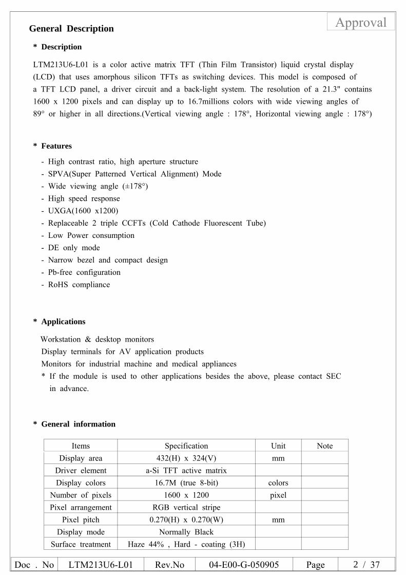
* General information
Items Specification Unit NoteDisplay area 432(H) x 324(V) mm
Driver element a-Si TFT active matrixDisplay colors 16.7M (true 8-bit) colors
Number of pixels 1600 x 1200 pixelPixel arrangement RGB vertical stripe
Pixel pitch 0.270(H) x 0.270(W) mmDisplay mode Normally Black
Surface treatment Haze 44% , Hard - coating (3H)
Doc . No LTM213U6-L01 Rev.No 04-E00-G-050905 Page 5 / 37
Approval
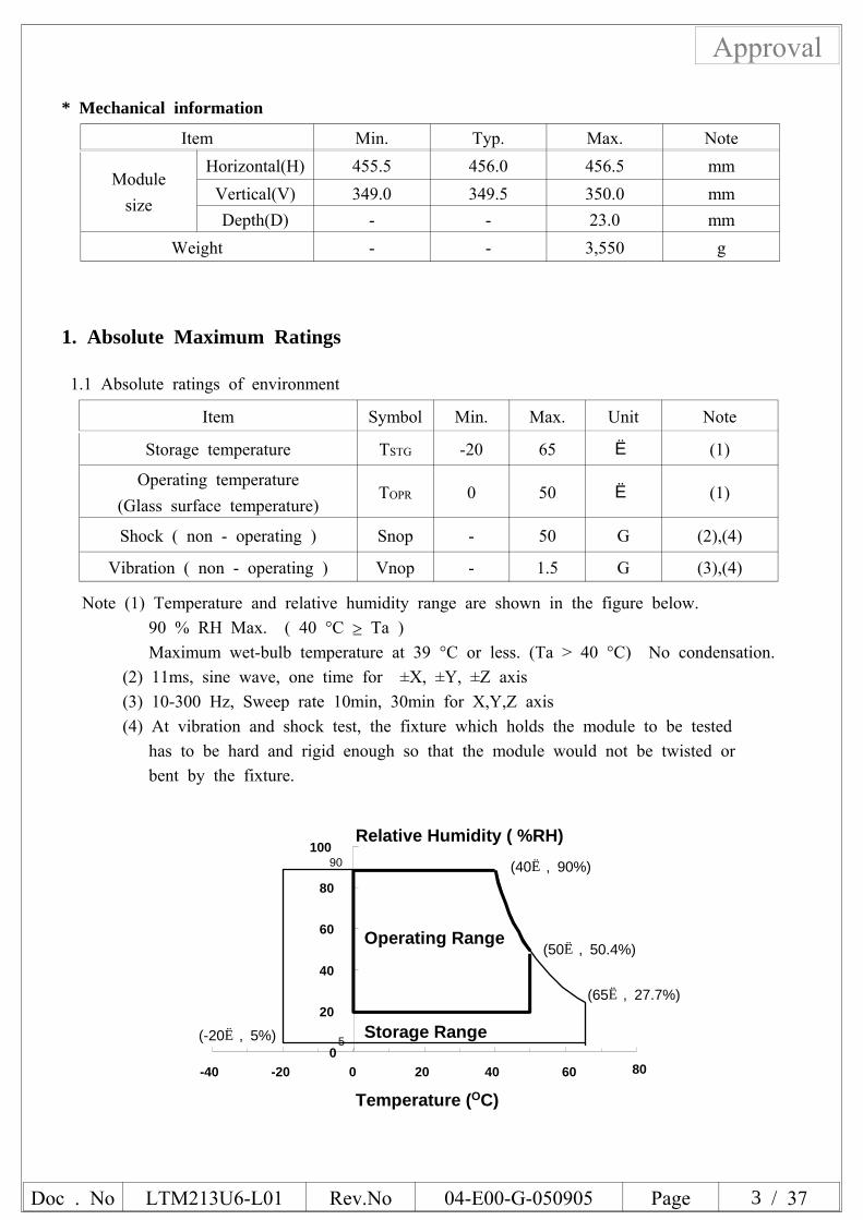
* Mechanical information
Item Min. Typ. Max. Note
Modulesize
Horizontal(H) 455.5 456.0 456.5 mmVertical(V) 349.0 349.5 350.0 mmDepth(D) - - 23.0 mm
Weight - - 3,550 g
1. Absolute Maximum Ratings
1.1 Absolute ratings of environment
Item Symbol Min. Max. Unit Note
Storage temperature TSTG -20 65 (1)
Operating temperature(Glass surface temperature)
TOPR 0 50 (1)
Shock ( non - operating ) Snop - 50 G (2),(4)
Vibration ( non - operating ) Vnop - 1.5 G (3),(4)
Note (1) Temperature and relative humidity range are shown in the figure below.90 % RH Max. ( 40 °C ≥ Ta )Maximum wet-bulb temperature at 39 °C or less. (Ta > 40 °C) No condensation.
(2) 11ms, sine wave, one time for ±X, ±Y, ±Z axis(3) 10-300 Hz, Sweep rate 10min, 30min for X,Y,Z axis(4) At vibration and shock test, the fixture which holds the module to be tested
has to be hard and rigid enough so that the module would not be twisted orbent by the fixture.
0
20
40
60
80
100
-40 -20 0 20 40 60 80
5
90
Operating Range
Storage Range
Relative Humidity ( %RH)
Temperature (OC)
(40, 90%)
(50, 50.4%)
(65, 27.7%)
(-20, 5%)
Doc . No LTM213U6-L01 Rev.No 04-E00-G-050905 Page 6 / 37
Approval
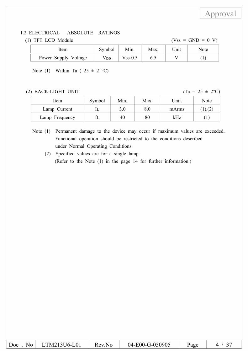
1.2 ELECTRICAL ABSOLUTE RATINGS(1) TFT LCD Module (Vss = GND = 0 V)
Item Symbol Min. Max. Unit Note
Power Supply Voltage VDD Vss-0.5 6.5 V (1)
Note (1) Within Ta ( 25 ± 2 °C)
(2) BACK-LIGHT UNIT (Ta = 25 ± 2°C)
Item Symbol Min. Max. Unit. Note
Lamp Current IL 3.0 8.0 mArms (1),(2)
Lamp Frequency fL 40 80 kHz (1)
Note (1) Permanent damage to the device may occur if maximum values are exceeded.Functional operation should be restricted to the conditions describedunder Normal Operating Conditions.
(2) Specified values are for a single lamp.(Refer to the Note (1) in the page 14 for further information.)
Doc . No LTM213U6-L01 Rev.No 04-E00-G-050905 Page 7 / 37
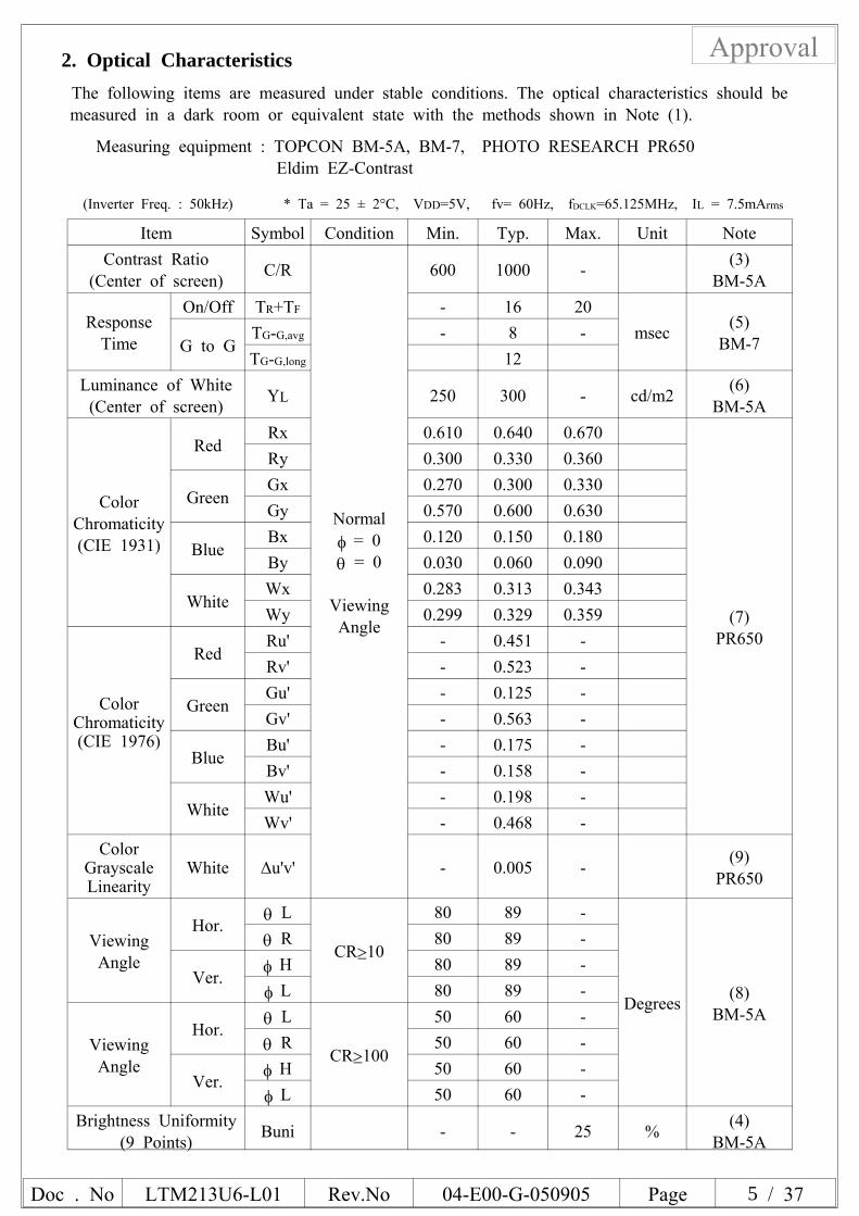
Approval2. Optical CharacteristicsThe following items are measured under stable conditions. The optical characteristics should bemeasured in a dark room or equivalent state with the methods shown in Note (1).
Measuring equipment : TOPCON BM-5A, BM-7, PHOTO RESEARCH PR650Eldim EZ-Contrast
(Inverter Freq. : 50kHz) * Ta = 25 ± 2°C, VDD=5V, fv= 60Hz, fDCLK=65.125MHz, IL = 7.5mArms
Item Symbol Condition Min. Typ. Max. Unit NoteContrast Ratio
(Center of screen) C/R
Normalφ = 0θ = 0
ViewingAngle
600 1000 - (3)BM-5A
ResponseTime
On/Off TR+TF - 16 20msec (5)
BM-7G to GTG-G,avg - 8 -TG-G,long 12
Luminance of White(Center of screen) YL 250 300 - cd/m2 (6)
BM-5A
ColorChromaticity(CIE 1931)
RedRx 0.610 0.640 0.670
(7)PR650
Ry 0.300 0.330 0.360
GreenGx 0.270 0.300 0.330Gy 0.570 0.600 0.630
BlueBx 0.120 0.150 0.180By 0.030 0.060 0.090
WhiteWx 0.283 0.313 0.343Wy 0.299 0.329 0.359
ColorChromaticity(CIE 1976)
RedRu' - 0.451 -Rv' - 0.523 -
GreenGu' - 0.125 -Gv' - 0.563 -
BlueBu' - 0.175 -Bv' - 0.158 -
WhiteWu' - 0.198 -Wv' - 0.468 -
ColorGrayscaleLinearity
White ∆u'v' - 0.005 - (9)PR650
ViewingAngle
Hor. θ L
CR≥10
80 89 -
Degrees (8)BM-5A
θ R 80 89 -
Ver. φ H 80 89 -φ L 80 89 -
ViewingAngle
Hor. θ L
CR≥100
50 60 -θ R 50 60 -
Ver. φ H 50 60 -φ L 50 60 -
Brightness Uniformity(9 Points) Buni - - 25 % (4)
BM-5A
Doc . No LTM213U6-L01 Rev.No 04-E00-G-050905 Page 8 / 37
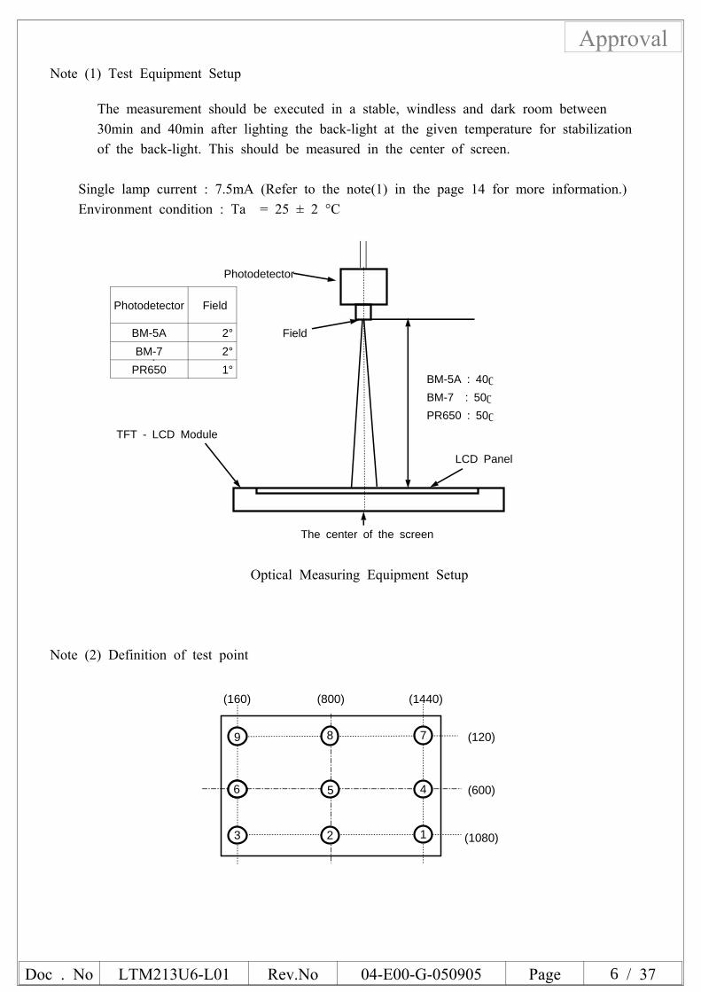
ApprovalNote (1) Test Equipment Setup
The measurement should be executed in a stable, windless and dark room between30min and 40min after lighting the back-light at the given temperature for stabilizationof the back-light. This should be measured in the center of screen.
Single lamp current : 7.5mA (Refer to the note(1) in the page 14 for more information.)Environment condition : Ta = 25 ± 2 °C
Photodetector
Photodetector Field
BM-5A 2°BM-7 2°
PR650 1°
LCD Panel
TFT - LCD Module
The center of the screen
BM-5A : 40BM-7 : 50PR650 : 50
Field
Optical Measuring Equipment Setup
Note (2) Definition of test point
(160) (1440)
(120)
(600)
(1080)1
(800)
9 8
5
23
6
7
4
Doc . No LTM213U6-L01 Rev.No 04-E00-G-050905 Page 9 / 37
ApprovalNote (3) Definition of Contrast Ratio (C/R)
: Ratio of gray max (Gmax) & gray min (Gmin) at the center point⑤ of the panel
CRGG
=maxmin
Gmax : Luminance with all pixels whiteGmin : Luminance with all pixels black
Note (4) Definition of 9 points brightness uniformity
BuniB B
B= ∗
−100
( max min)max
Bmax : Maximum brightnessBmin : Minimum brightness
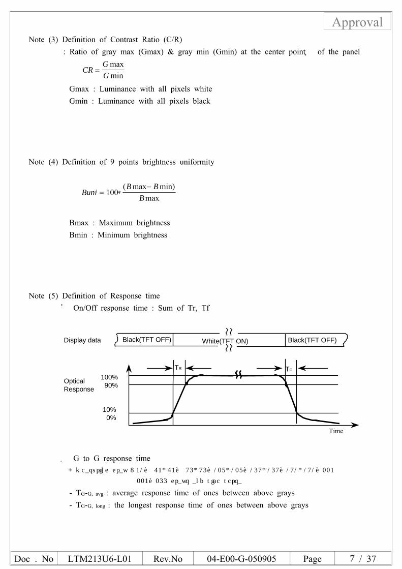
Note (5) Definition of Response time① On/Off response time : Sum of Tr, Tf
Display data White(TFT ON)Black(TFT OFF) Black(TFT OFF)
OpticalResponse
100% 90%
10% 0%
TR TF
Time
② G to G response time- measuring gray : 31→ 63, 63→ 95, 95→127, 127→159, 159→191, 191→223
223→255 grays and vice versa
- TG-G, avg : average response time of ones between above grays- TG-G, long : the longest response time of ones between above grays
Doc . No LTM213U6-L01 Rev.No 04-E00-G-050905 Page 10 / 37
ApprovalNote (6) Definition of Luminance of White : Luminance of white at center point⑤
Note (7) Definition of Color Chromaticity (CIE 1931, CIE1976)Color coordinate of Red, Green, Blue & White at center point⑤
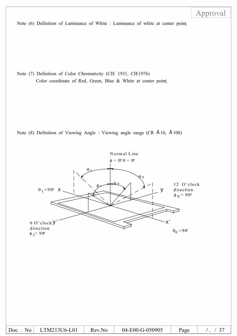
Note (8) Definition of Viewing Angle : Viewing angle range (CR ≥10, ≥100)
6 O ’c lockd irec tion
N orm al L ine
θ Lθ R
φ Hφ L 12 O ’c lockd irec tion
θR = 90 o
θ L = 90 o
φ = 0 o,
x
x’y ’
y
θ = 0 o
φ H = 90 o
φ L= 90 o
Doc . No LTM213U6-L01 Rev.No 04-E00-G-050905 Page 11 / 37
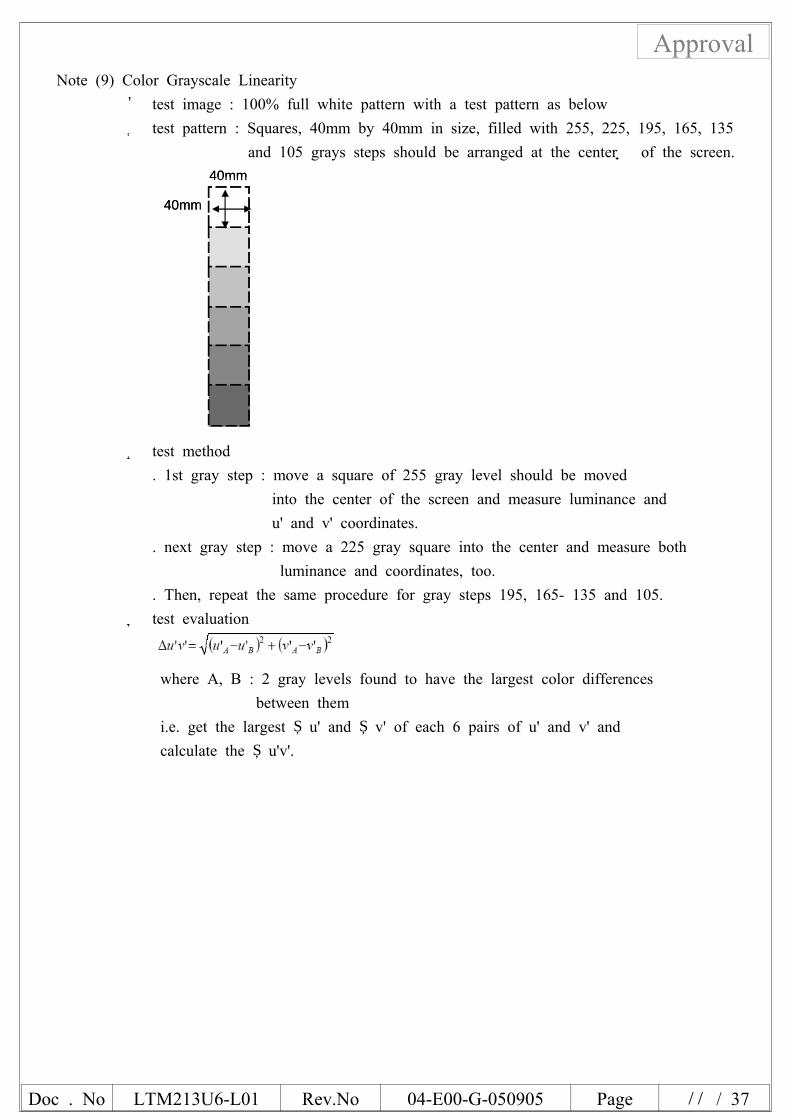
ApprovalNote (9) Color Grayscale Linearity
① test image : 100% full white pattern with a test pattern as below② test pattern : Squares, 40mm by 40mm in size, filled with 255, 225, 195, 165, 135
and 105 grays steps should be arranged at the center⑤ of the screen.40mm
40mm
40mm
40mm
③ test method. 1st gray step : move a square of 255 gray level should be moved
into the center of the screen and measure luminance andu' and v' coordinates.
. next gray step : move a 225 gray square into the center and measure bothluminance and coordinates, too.
. Then, repeat the same procedure for gray steps 195, 165- 135 and 105.④ test evaluation
where A, B : 2 gray levels found to have the largest color differencesbetween them
i.e. get the largest Δu' and Δv' of each 6 pairs of u' and v' andcalculate the Δu'v'.
Doc . No LTM213U6-L01 Rev.No 04-E00-G-050905 Page 12 / 37
Approval3. Electrical Characteristics
3.1 TFT LCD MODULETa = 25°C
Item Symbol Min. Typ. Max. Unit NoteVoltage of Power Supply VDD 4.5 5.0 5.5 V (1)
Interface type LVDS LRU6122M0(LVDS embeded T-con)Current of
PowerSupply
(a) BlackIDD
- 1000 - mA(2),(3)(b) White - 1400 - mA
(c) 2Line Vertical - 1400 1600 mAVsync Frequency fV 59 60 61 Hz
2pxl/clkHsync Frequency fH 72 74 76 kHz
Main Frequency fDCLK 64.0 65.125 66.25 MHz
Rush Current IRUSH - - 4.0 A (4)
Note (1) The connector for display data & timing signal should be connected.(Vss=0V)(2) fV=60Hz, fDCLK =65.125MHz, VDD = 5.0V, DC Current.(3) Power dissipation check pattern(LCD Module only)
a) Black Pattern b) White Pattern
R G B R G B
R G B R G B
R G B R G B
R G B R G B
R G B R G
R G B R GR G B R G B
R G B R G B
R G B R G B
R G B R G B
R G B R G B
R G B R G B
G B R G B
G B R G B
B
R G B
R G B
R G B
R G B
R G
R G
c) 2Line Vertical stripe pattern
R G B R G B
R G B R G B
R G B R G B
R G B R G B
R G B R G
R G B R GR G B R G B
R G B R G B
R G B R G B
R G B R G B
R G B R G B
R G B R G B
G B R G B
G B R G B
B
R G B
R G B
R G B
R G B
R G
R G
R G B R G B
R G B R G B
R G B R G B
R G B R G B
R G B R G
R G B R GR G B R G B
R G B R G B
R G B R G B
R G B R G B
R G B R G B
R G B R G B
G B R G B
G B R G B
B
R G B
R G B
R G B
R G B
R G
R G
R G B R G B
R G B R G B
R G B R G B
R G B R G B
R G B R G
R G B R GR G B R G B
R G B R G B
R G B R G B
R G B R G B
R G B R G B
R G B R G B
G B R G B
G B R G B
B
R G B
R G B
R G B
R G B
R G
R G
R G B R G B
R G B R G B
R G B R G B
R G B R G B
R G B R G
R G B R GR G B R G B
R G B R G B
R G B R G B
R G B R G B
R G B R G B
R G B R G B
G B R G B
G B R G B
B
R G B
R G B
R G B
R G B
R G
R G
c) 2Line Vertical stripe pattern
R G B R G B
R G B R G B
R G B R G B
R G B R G B
R G B R G
R G B R GR G B R G B
R G B R G B
R G B R G B
R G B R G B
R G B R G B
R G B R G B
G B R G B
G B R G B
B
R G B
R G B
R G B
R G B
R G
R G
R G B R G B
R G B R G B
R G B R G B
R G B R G B
R G B R G
R G B R GR G B R G B
R G B R G B
R G B R G B
R G B R G B
R G B R G B
R G B R G B
G B R G B
G B R G B
B
R G B
R G B
R G B
R G B
R G
R G
R G B R G B
R G B R G B
R G B R G B
R G B R G B
R G B R G
R G B R GR G B R G B
R G B R G B
R G B R G B
R G B R G B
R G B R G B
R G B R G B
G B R G B
G B R G B
B
R G B
R G B
R G B
R G B
R G
R G
Doc . No LTM213U6-L01 Rev.No 04-E00-G-050905 Page 13 / 37
Approval(4) Measurement Conditions
5V
12V
VDD ( LCD INPUT)
CONTROL SIGNAL(HIGH to LOW)
M22SK1399
M12SK1059
R2
1K
C2
10000pFC31uF
R3
47K
R147K
FUSE C11uF
Control Signal : High(+5V) → Low(Ground)All Signal lines to panel, except for power 5V : GroundThe rising time of supplied voltage is controlled to 470us by R3 and C2 value.
0.9 VDD
0.1 VDD
Rising Time
GND
5V
Doc . No LTM213U6-L01 Rev.No 04-E00-G-050905 Page 14 / 37
Approval3.2 BACK-LIGHT UNIT
The back-light system is an edge - lighting type with 2 triple CCFTs (Cold CathodeFluorescent Tube). The characteristics of two triple lamps are shown in the following tables.
Ta=25 ± 2°C
Item Symbol Min. Typ. Max. Unit NoteLamp Current IL 3.0 7.5 8.0 mArms (1)Lamp Voltage VL - 740 - Vrms
Lamp Frequency fL 40 - 60 kHz (2)
inverterwaveform
asymmetryrate
Wasy - - 10 % (5)
distortionrate
Wdis - - √2 ±10 %
Startup Voltage Vs - -0 : 1,800
Vrms (3)25: 1,440
Note) The waveform of the inverter output voltage must be area symmetric and the designof the inverter must have specifications for the modularized lamp.
The performance of the back-light, for example life time or brightness, is much influenced by thecharacteristics of the DC-AC inverter for the lamp. So all the parameters of an inverter should becarefully designed so as not to produce too much leakage current from high-voltage output of theinverter. When you design or order the inverter, please make sure that a poor lighting caused by themismatch of the back-light and the inverter(miss lighting, flicker, etc.) never occur. When you confirmit, the module should be operated in the same condition as it is installed in your instrument.
Note (1) Lamp current is measured with current meter for high frequency as shown below.Refer to the block diagram of the back-light unit in the next page for more information.Specified values are for a single lamp.
Inverter :FIF2066-01BHOT(WHITE)
LCD Module InverterHOT(BLUE)
COLD(BLACK)HOT(GLAY)
A
COLD(WHITE)A
A
COLD(GRAYBLUE)
(2) Lamp frequency may produce interference with horizontal synchronous frequency which maycause line flow on the display. Therefore lamp frequency should be detached from thehorizontal synchronous frequency and its harmonics as far as possible in order to avoidinterference.
(3) If an inverter has shutdown function it should keep its output for more than 1 second even ifthe lamp connector open. Otherwise the lamps may not to be turned on.
Doc . No LTM213U6-L01 Rev.No 04-E00-G-050905 Page 15 / 37
Approval(4) Because the inverter uses high voltage, please disconnect it from the power before
assembling or disassembling.(5) The output of the inverter must have symmetrical(negative and positive) voltage waveform
and current waveform.Please do not use the inverter which has unsymmetrical voltage and current and spike wave.Designing a system inverter intended to have better display performance,power efficiency and lamp reliability, please follow the requirements the below.They would help increase the lamp lifetime and reduce leakage current.
a. The asymmetry rate of the inverter waveform should be less than 10%.b. The distortion rate of the waveform should be within √2 ±10%.
* Inverter output waveform had better be more similar to ideal sine wave.
I p
I -p
* Asymmetry rate:| I p – I –p | / Irms x 100%
* Distortion rateI p (or I –p) / Irms
I p
I -p
I p
I -p
* Asymmetry rate:| I p – I –p | / Irms x 100%
* Distortion rateI p (or I –p) / Irms
Doc . No LTM213U6-L01 Rev.No 04-E00-G-050905 Page 16 / 37
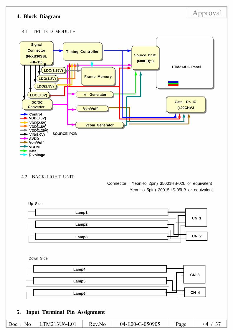
Approval4. Block Diagram
4.1 TFT LCD MODULE
SignalConnector
(FI-XB30SSL-HF-15)
DC/DCConverter
γ Generator
Vcom Generator
LTM213U6 Panel
SOURCE PCB
ControlVDD(3.3V)
VIN(5.0V)AVDDVon/VoffVCOM
Gate Dr. IC(400CH)*3
ΥVoltage
Timing Controller
Von/Voff
Source Dr.IC(600CH)*8
LDO(3.3V)
Frame Memory
LDO(2.5V)
LDO(1.8V)
VDD(2.5V)VDD(1.8V)
LDO(1.25V)
VDD(1.25V)
Data
4.2 BACK-LIGHT UNITConnector : YeonHo 2pin) 35001HS-02L or equivalent
YeonHo 5pin) 20015HS-05LB or equivalent
Lamp1
Lamp2
Lamp3
CN 1
CN 2
Lamp4
Lamp5
Lamp6
CN 3
CN 4
Up Side
Down Side
5. Input Terminal Pin Assignment
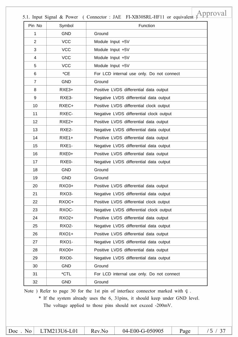
Doc . No LTM213U6-L01 Rev.No 04-E00-G-050905 Page 17 / 37
Approval5.1. Input Signal & Power ( Connector : JAE FI-XB30SRL-HF11 or equivalent )
Pin No Symbol Function
1 GND Ground
2 VCC Module Input +5V
3 VCC Module Input +5V
4 VCC Module Input +5V
5 VCC Module Input +5V
6 *CE For LCD internal use only. Do not connect
7 GND Ground
8 RXE3+ Positive LVDS differential data output
9 RXE3- Negative LVDS differential data output
10 RXEC+ Positive LVDS differential clock output
11 RXEC- Negative LVDS differential clock output
12 RXE2+ Positive LVDS differential data output
13 RXE2- Negative LVDS differential data output
14 RXE1+ Positive LVDS differential data output
15 RXE1- Negative LVDS differential data output
16 RXE0+ Positive LVDS differential data output
17 RXE0- Negative LVDS differential data output
18 GND Ground
19 GND Ground
20 RXO3+ Positive LVDS differential data output
21 RXO3- Negative LVDS differential data output
22 RXOC+ Positive LVDS differential clock output
23 RXOC- Negative LVDS differential clock output
24 RXO2+ Positive LVDS differential data output
25 RXO2- Negative LVDS differential data output
26 RXO1+ Positive LVDS differential data output
27 RXO1- Negative LVDS differential data output
28 RXO0+ Positive LVDS differential data output
29 RXO0- Negative LVDS differential data output
30 GND Ground
31 *CTL For LCD internal use only. Do not connect
32 GND Ground
Note ) Refer to page 30 for the 1st pin of interface connector marked with .* If the system already uses the 6, 31pins, it should keep under GND level.
The voltage applied to those pins should not exceed -200mV.
Doc . No LTM213U6-L01 Rev.No 04-E00-G-050905 Page 18 / 37
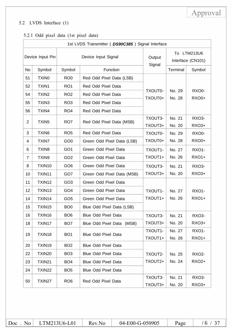
Approval5.2 LVDS Interface (1)
5.2.1 Odd pixel data (1st pixel data)
1st LVDS Transmitter ( DS90C385 ) Signal Interface
Device Input Pin Device Input Signal Output
Signal
To LTM213U6
Interface (CN101)
No Symbol Symbol Function Terminal Symbol
51 TXIN0 RO0 Red Odd Pixel Data (LSB)
TXOUT0-
TXOUT0+
No. 29
No. 28
RXO0-
RXO0+
52 TXIN1 RO1 Red Odd Pixel Data
54 TXIN2 RO2 Red Odd Pixel Data
55 TXIN3 RO3 Red Odd Pixel Data
56 TXIN4 RO4 Red Odd Pixel Data
2 TXIN5 RO7 Red Odd Pixel Data (MSB)TXOUT3-
TXOUT3+
No. 21
No. 20
RXO3-
RXO3+
3 TXIN6 RO5 Red Odd Pixel Data TXOUT0-
TXOUT0+
No. 29
No. 28
RXO0-
RXO0+4 TXIN7 GO0 Green Odd Pixel Data (LSB)
6 TXIN8 GO1 Green Odd Pixel Data TXOUT1-
TXOUT1+
No. 27
No. 26
RXO1-
RXO1+7 TXIN9 GO2 Green Odd Pixel Data
8 TXIN10 GO6 Green Odd Pixel Data TXOUT3-
TXOUT3+
No. 21
No. 20
RXO3-
RXO3+10 TXIN11 GO7 Green Odd Pixel Data (MSB)
11 TXIN12 GO3 Green Odd Pixel Data
TXOUT1-
TXOUT1+
No. 27
No. 26
RXO1-
RXO1+
12 TXIN13 GO4 Green Odd Pixel Data
14 TXIN14 GO5 Green Odd Pixel Data
15 TXIN15 BO0 Blue Odd Pixel Data (LSB)
16 TXIN16 BO6 Blue Odd Pixel Data TXOUT3-
TXOUT3+
No. 21
No. 20
RXO3-
RXO3+18 TXIN17 BO7 Blue Odd Pixel Data (MSB)
19 TXIN18 BO1 Blue Odd Pixel DataTXOUT1-
TXOUT1+
No. 27
No. 26
RXO1-
RXO1+
20 TXIN19 BO2 Blue Odd Pixel Data
TXOUT2-
TXOUT2+
No. 25
No. 24
RXO2-
RXO2+
22 TXIN20 BO3 Blue Odd Pixel Data
23 TXIN21 BO4 Blue Odd Pixel Data
24 TXIN22 BO5 Blue Odd Pixel Data
50 TXIN27 RO6 Red Odd Pixel DataTXOUT3-
TXOUT3+
No. 21
No. 20
RXO3-
RXO3+
Doc . No LTM213U6-L01 Rev.No 04-E00-G-050905 Page 19 / 37
Approval
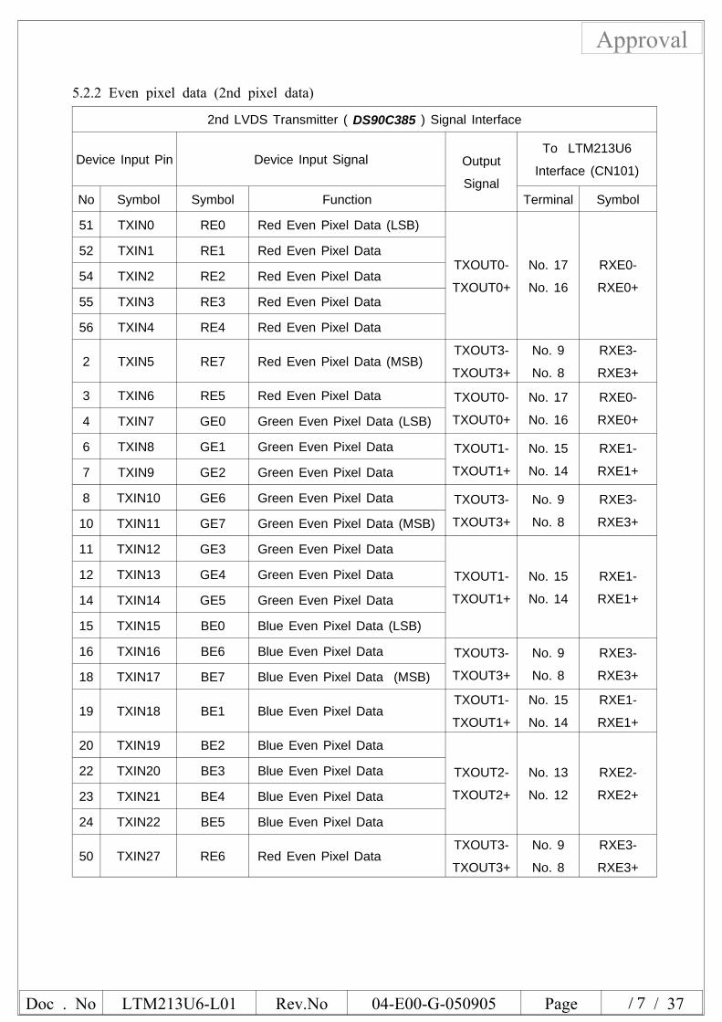
5.2.2 Even pixel data (2nd pixel data)
2nd LVDS Transmitter ( DS90C385 ) Signal Interface
Device Input Pin Device Input Signal Output
Signal
To LTM213U6
Interface (CN101)
No Symbol Symbol Function Terminal Symbol
51 TXIN0 RE0 Red Even Pixel Data (LSB)
TXOUT0-
TXOUT0+
No. 17
No. 16
RXE0-
RXE0+
52 TXIN1 RE1 Red Even Pixel Data
54 TXIN2 RE2 Red Even Pixel Data
55 TXIN3 RE3 Red Even Pixel Data
56 TXIN4 RE4 Red Even Pixel Data
2 TXIN5 RE7 Red Even Pixel Data (MSB)TXOUT3-
TXOUT3+
No. 9
No. 8
RXE3-
RXE3+
3 TXIN6 RE5 Red Even Pixel Data TXOUT0-
TXOUT0+
No. 17
No. 16
RXE0-
RXE0+4 TXIN7 GE0 Green Even Pixel Data (LSB)
6 TXIN8 GE1 Green Even Pixel Data TXOUT1-
TXOUT1+
No. 15
No. 14
RXE1-
RXE1+7 TXIN9 GE2 Green Even Pixel Data
8 TXIN10 GE6 Green Even Pixel Data TXOUT3-
TXOUT3+
No. 9
No. 8
RXE3-
RXE3+10 TXIN11 GE7 Green Even Pixel Data (MSB)
11 TXIN12 GE3 Green Even Pixel Data
TXOUT1-
TXOUT1+
No. 15
No. 14
RXE1-
RXE1+
12 TXIN13 GE4 Green Even Pixel Data
14 TXIN14 GE5 Green Even Pixel Data
15 TXIN15 BE0 Blue Even Pixel Data (LSB)
16 TXIN16 BE6 Blue Even Pixel Data TXOUT3-
TXOUT3+
No. 9
No. 8
RXE3-
RXE3+18 TXIN17 BE7 Blue Even Pixel Data (MSB)
19 TXIN18 BE1 Blue Even Pixel DataTXOUT1-
TXOUT1+
No. 15
No. 14
RXE1-
RXE1+
20 TXIN19 BE2 Blue Even Pixel Data
TXOUT2-
TXOUT2+
No. 13
No. 12
RXE2-
RXE2+
22 TXIN20 BE3 Blue Even Pixel Data
23 TXIN21 BE4 Blue Even Pixel Data
24 TXIN22 BE5 Blue Even Pixel Data
50 TXIN27 RE6 Red Even Pixel DataTXOUT3-
TXOUT3+
No. 9
No. 8
RXE3-
RXE3+
Doc . No LTM213U6-L01 Rev.No 04-E00-G-050905 Page 20 / 37
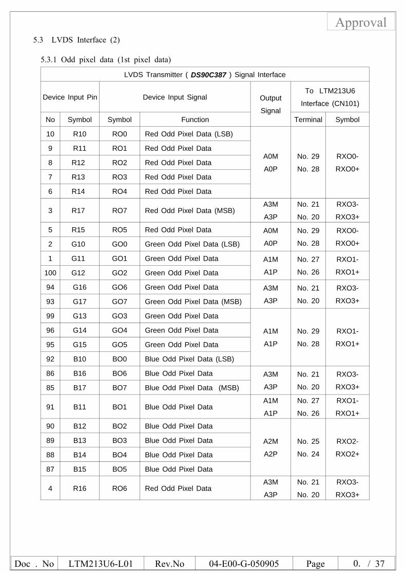
Approval5.3 LVDS Interface (2)
5.3.1 Odd pixel data (1st pixel data)
LVDS Transmitter ( DS90C387 ) Signal Interface
Device Input Pin Device Input Signal Output
Signal
To LTM213U6
Interface (CN101)
No Symbol Symbol Function Terminal Symbol
10 R10 RO0 Red Odd Pixel Data (LSB)
A0M
A0P
No. 29
No. 28
RXO0-
RXO0+
9 R11 RO1 Red Odd Pixel Data
8 R12 RO2 Red Odd Pixel Data
7 R13 RO3 Red Odd Pixel Data
6 R14 RO4 Red Odd Pixel Data
3 R17 RO7 Red Odd Pixel Data (MSB)A3M
A3P
No. 21
No. 20
RXO3-
RXO3+
5 R15 RO5 Red Odd Pixel Data A0M
A0P
No. 29
No. 28
RXO0-
RXO0+2 G10 GO0 Green Odd Pixel Data (LSB)
1 G11 GO1 Green Odd Pixel Data A1M
A1P
No. 27
No. 26
RXO1-
RXO1+100 G12 GO2 Green Odd Pixel Data
94 G16 GO6 Green Odd Pixel Data A3M
A3P
No. 21
No. 20
RXO3-
RXO3+93 G17 GO7 Green Odd Pixel Data (MSB)
99 G13 GO3 Green Odd Pixel Data
A1M
A1P
No. 29
No. 28
RXO1-
RXO1+
96 G14 GO4 Green Odd Pixel Data
95 G15 GO5 Green Odd Pixel Data
92 B10 BO0 Blue Odd Pixel Data (LSB)
86 B16 BO6 Blue Odd Pixel Data A3M
A3P
No. 21
No. 20
RXO3-
RXO3+85 B17 BO7 Blue Odd Pixel Data (MSB)
91 B11 BO1 Blue Odd Pixel DataA1M
A1P
No. 27
No. 26
RXO1-
RXO1+
90 B12 BO2 Blue Odd Pixel Data
A2M
A2P
No. 25
No. 24
RXO2-
RXO2+
89 B13 BO3 Blue Odd Pixel Data
88 B14 BO4 Blue Odd Pixel Data
87 B15 BO5 Blue Odd Pixel Data
4 R16 RO6 Red Odd Pixel DataA3M
A3P
No. 21
No. 20
RXO3-
RXO3+
Doc . No LTM213U6-L01 Rev.No 04-E00-G-050905 Page 21 / 37
Approval
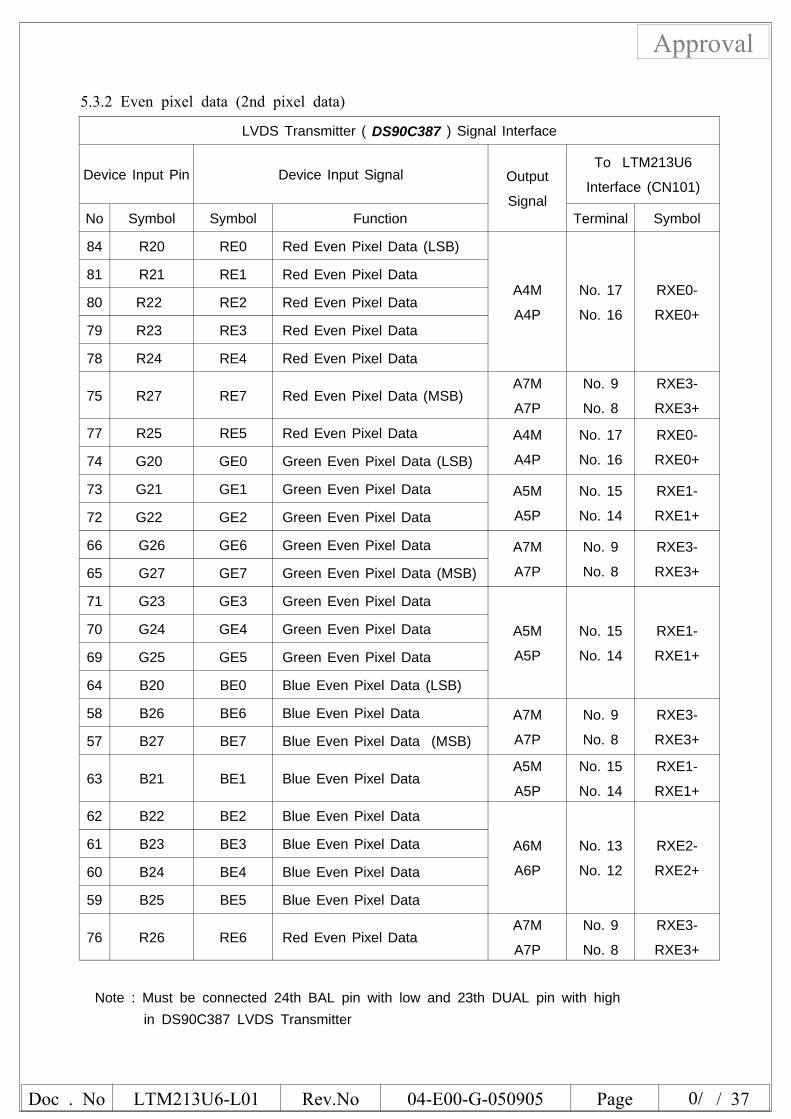
5.3.2 Even pixel data (2nd pixel data)
LVDS Transmitter ( DS90C387 ) Signal Interface
Device Input Pin Device Input Signal Output
Signal
To LTM213U6
Interface (CN101)
No Symbol Symbol Function Terminal Symbol
84 R20 RE0 Red Even Pixel Data (LSB)
A4M
A4P
No. 17
No. 16
RXE0-
RXE0+
81 R21 RE1 Red Even Pixel Data
80 R22 RE2 Red Even Pixel Data
79 R23 RE3 Red Even Pixel Data
78 R24 RE4 Red Even Pixel Data
75 R27 RE7 Red Even Pixel Data (MSB)A7M
A7P
No. 9
No. 8
RXE3-
RXE3+
77 R25 RE5 Red Even Pixel Data A4M
A4P
No. 17
No. 16
RXE0-
RXE0+74 G20 GE0 Green Even Pixel Data (LSB)
73 G21 GE1 Green Even Pixel Data A5M
A5P
No. 15
No. 14
RXE1-
RXE1+72 G22 GE2 Green Even Pixel Data
66 G26 GE6 Green Even Pixel Data A7M
A7P
No. 9
No. 8
RXE3-
RXE3+65 G27 GE7 Green Even Pixel Data (MSB)
71 G23 GE3 Green Even Pixel Data
A5M
A5P
No. 15
No. 14
RXE1-
RXE1+
70 G24 GE4 Green Even Pixel Data
69 G25 GE5 Green Even Pixel Data
64 B20 BE0 Blue Even Pixel Data (LSB)
58 B26 BE6 Blue Even Pixel Data A7M
A7P
No. 9
No. 8
RXE3-
RXE3+57 B27 BE7 Blue Even Pixel Data (MSB)
63 B21 BE1 Blue Even Pixel DataA5M
A5P
No. 15
No. 14
RXE1-
RXE1+
62 B22 BE2 Blue Even Pixel Data
A6M
A6P
No. 13
No. 12
RXE2-
RXE2+
61 B23 BE3 Blue Even Pixel Data
60 B24 BE4 Blue Even Pixel Data
59 B25 BE5 Blue Even Pixel Data
76 R26 RE6 Red Even Pixel DataA7M
A7P
No. 9
No. 8
RXE3-
RXE3+
Note : Must be connected 24th BAL pin with low and 23th DUAL pin with highin DS90C387 LVDS Transmitter
Doc . No LTM213U6-L01 Rev.No 04-E00-G-050905 Page 22 / 37
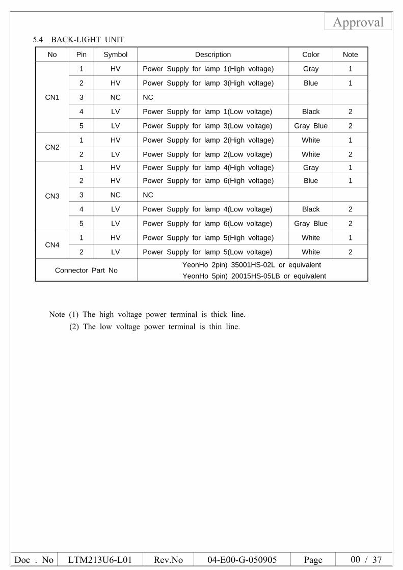
Approval5.4 BACK-LIGHT UNIT
No Pin Symbol Description Color Note
CN1
1 HV Power Supply for lamp 1(High voltage) Gray 1
2 HV Power Supply for lamp 3(High voltage) Blue 1
3 NC NC
4 LV Power Supply for lamp 1(Low voltage) Black 2
5 LV Power Supply for lamp 3(Low voltage) Gray Blue 2
CN21 HV Power Supply for lamp 2(High voltage) White 1
2 LV Power Supply for lamp 2(Low voltage) White 2
CN3
1 HV Power Supply for lamp 4(High voltage) Gray 1
2 HV Power Supply for lamp 6(High voltage) Blue 1
3 NC NC
4 LV Power Supply for lamp 4(Low voltage) Black 2
5 LV Power Supply for lamp 6(Low voltage) Gray Blue 2
CN41 HV Power Supply for lamp 5(High voltage) White 1
2 LV Power Supply for lamp 5(Low voltage) White 2
Connector Part NoYeonHo 2pin) 35001HS-02L or equivalentYeonHo 5pin) 20015HS-05LB or equivalent
Note (1) The high voltage power terminal is thick line.(2) The low voltage power terminal is thin line.
Doc . No LTM213U6-L01 Rev.No 04-E00-G-050905 Page 23 / 37
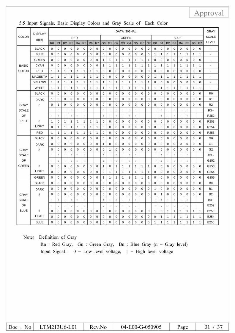
Approval5.5 Input Signals, Basic Display Colors and Gray Scale of Each Color
COLORDISPLAY
(8bit)
DATA SIGNAL GRAY
SCALE
LEVELRED GREEN BLUE
R0 R1 R2 R3 R4 R5 R6 R7 G0 G1 G2 G3 G4 G5 G6 G7 B0 B1 B2 B3 B4 B5 B6 B7
BASIC
COLOR
BLACK 0 0 0 0 0 0 0 0 0 0 0 0 0 0 0 0 0 0 0 0 0 0 0 0 -
BLUE 0 0 0 0 0 0 0 0 0 0 0 0 0 0 0 0 1 1 1 1 1 1 1 1 -
GREEN 0 0 0 0 0 0 0 0 1 1 1 1 1 1 1 1 0 0 0 0 0 0 0 0 -
CYAN 0 0 0 0 0 0 0 0 1 1 1 1 1 1 1 1 1 1 1 1 1 1 1 1 -
RED 1 1 1 1 1 1 1 1 0 0 0 0 0 0 0 0 0 0 0 0 0 0 0 0 -
MAGENTA 1 1 1 1 1 1 1 1 0 0 0 0 0 0 0 0 1 1 1 1 1 1 1 1 -
YELLOW 1 1 1 1 1 1 1 1 1 1 1 1 1 1 1 1 0 0 0 0 0 0 0 0 -
WHITE 1 1 1 1 1 1 1 1 1 1 1 1 1 1 1 1 1 1 1 1 1 1 1 1 -
GRAY
SCALE
OF
RED
BLACK 0 0 0 0 0 0 0 0 0 0 0 0 0 0 0 0 0 0 0 0 0 0 0 0 R0
DARK
↑
↓
LIGHT
1 0 0 0 0 0 0 0 0 0 0 0 0 0 0 0 0 0 0 0 0 0 0 0 R1
0 1 0 0 0 0 0 0 0 0 0 0 0 0 0 0 0 0 0 0 0 0 0 0 R2
: : : : : : : : : : : : : : : : : : R3~
R252: : : : : : : : : : : : : : : : : :
1 0 1 1 1 1 1 1 0 0 0 0 0 0 0 0 0 0 0 0 0 0 0 0 R253
0 1 1 1 1 1 1 1 0 0 0 0 0 0 0 0 0 0 0 0 0 0 0 0 R254
RED 1 1 1 1 1 1 1 1 0 0 0 0 0 0 0 0 0 0 0 0 0 0 0 0 R255
GRAY
SCALE
OF
GREEN
BLACK 0 0 0 0 0 0 0 0 0 0 0 0 0 0 0 0 0 0 0 0 0 0 0 0 G0
DARK
↑
↓
LIGHT
0 0 0 0 0 0 0 0 1 0 0 0 0 0 0 0 0 0 0 0 0 0 0 0 G1
0 0 0 0 0 0 0 0 0 1 0 0 0 0 0 0 0 0 0 0 0 0 0 0 G2
: : : : : : : : : : : : : : : : : : G3~
G252: : : : : : : : : : : : : : : : : :
0 0 0 0 0 0 0 0 1 0 1 1 1 1 1 1 0 0 0 0 0 0 0 0 G253
0 0 0 0 0 0 0 0 0 1 1 1 1 1 1 1 0 0 0 0 0 0 0 0 G254
GREEN 0 0 0 0 0 0 0 0 1 1 1 1 1 1 1 1 0 0 0 0 0 0 0 0 G255
GRAY
SCALE
OF
BLUE
BLACK 0 0 0 0 0 0 0 0 0 0 0 0 0 0 0 0 0 0 0 0 0 0 0 0 B0
DARK
↑
↓
LIGHT
0 0 0 0 0 0 0 0 0 0 0 0 0 0 0 0 1 0 0 0 0 0 0 0 B1
0 0 0 0 0 0 0 0 0 0 0 0 0 0 0 0 0 1 0 0 0 0 0 0 B2
: : : : : : : : : : : : : : : : : : B3~
B252: : : : : : : : : : : : : : : : : :
0 0 0 0 0 0 0 0 0 0 0 0 0 0 0 0 1 0 1 1 1 1 1 1 B253
0 0 0 0 0 0 0 0 0 0 0 0 0 0 0 0 0 1 1 1 1 1 1 1 B254
BLUE 0 0 0 0 0 0 0 0 0 0 0 0 0 0 0 0 1 1 1 1 1 1 1 1 B255
Note) Definition of GrayRn : Red Gray, Gn : Green Gray, Bn : Blue Gray (n = Gray level)Input Signal : 0 = Low level voltage, 1 = High level voltage
Doc . No LTM213U6-L01 Rev.No 04-E00-G-050905 Page 24 / 37
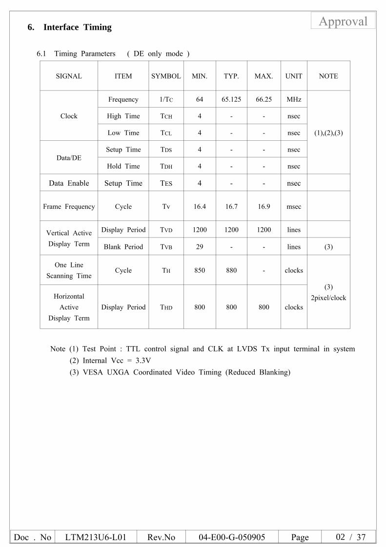
Approval6. Interface Timing
6.1 Timing Parameters ( DE only mode )
SIGNAL ITEM SYMBOL MIN. TYP. MAX. UNIT NOTE
Clock
Frequency 1/TC 64 65.125 66.25 MHz
(1),(2),(3)
High Time TCH 4 - - nsec
Low Time TCL 4 - - nsec
Data/DESetup Time TDS 4 - - nsec
Hold Time TDH 4 - - nsec
Data Enable Setup Time TES 4 - - nsec
Frame Frequency Cycle Tv 16.4 16.7 16.9 msec
Vertical ActiveDisplay Term
Display Period TVD 1200 1200 1200 lines
Blank Period TVB 29 - - lines (3)
One LineScanning Time
Cycle TH 850 880 - clocks
(3)2pixel/clockHorizontal
ActiveDisplay Term
Display Period THD 800 800 800 clocks
Note (1) Test Point : TTL control signal and CLK at LVDS Tx input terminal in system(2) Internal Vcc = 3.3V(3) VESA UXGA Coordinated Video Timing (Reduced Blanking)
Doc . No LTM213U6-L01 Rev.No 04-E00-G-050905 Page 25 / 37
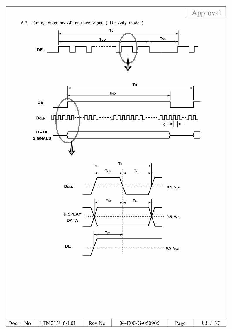
Approval6.2 Timing diagrams of interface signal ( DE only mode )
DATASIGNALS
DE
TVD
TV
TH
DCLK
TC
DE
THD
TVB
0.5 VCC
TES
TDS TDH
TCH TCL
TC
DE
DISPLAYDATA
DCLK
0.5 VCC
0.5 VCC
Doc . No LTM213U6-L01 Rev.No 04-E00-G-050905 Page 26 / 37
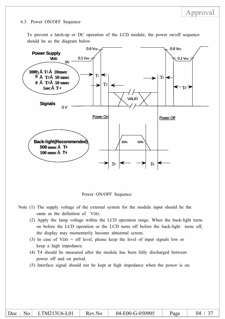
Approval6.3 Power ON/OFF Sequence
To prevent a latch-up or DC operation of the LCD module, the power on/off sequenceshould be as the diagram below.
Power SupplyVDD
0.9 VDD 0.9 VDD
0V
0 V
VALIDSignals
T3
300≤T1 ≤ 10msec0 ≤ T2 ≤ 50 msec0 ≤ T3 ≤ 50 msec
1sec ≤ T 4
T1
T2T4
0.1 VDD 0.1 VDD
Back-light(Recommended)500 msec ≤ T5
100 msec≤ T6
Power On Power Off
T5 T6
50% 50%
Power SupplyVDD
0.9 VDD 0.9 VDD
0V
0 V
VALIDSignals
T3
300≤T1 ≤ 10msec0 ≤ T2 ≤ 50 msec0 ≤ T3 ≤ 50 msec
1sec ≤ T 4
T1
T2T4
0.1 VDD 0.1 VDD
Back-light(Recommended)500 msec ≤ T5
100 msec≤ T6
Power On Power Off
T5 T6
50% 50%
Power ON/OFF Sequence
Note (1) The supply voltage of the external system for the module input should be thesame as the definition of VDD.
(2) Apply the lamp voltage within the LCD operation range. When the back-light turnson before the LCD operation or the LCD turns off before the back-light turns off,the display may momentarily become abnormal screen.
(3) In case of VDD = off level, please keep the level of input signals low orkeep a high impedance.
(4) T4 should be measured after the module has been fully discharged betweenpower off and on period.
(5) Interface signal should not be kept at high impedance when the power is on.
Doc . No LTM213U6-L01 Rev.No 04-E00-G-050905 Page 27 / 37
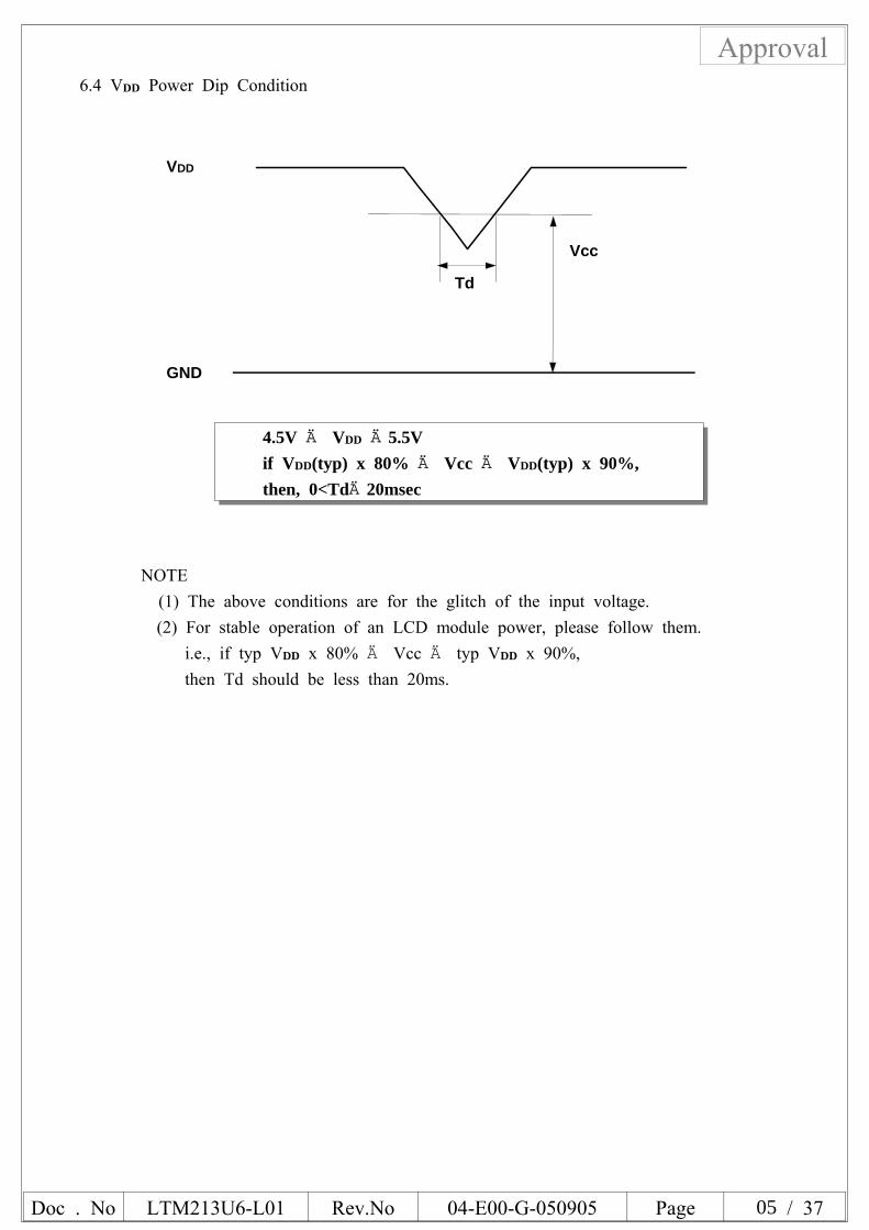
Approval6.4 VDD Power Dip Condition
4.5V ≤ VDD ≤5.5Vif VDD(typ) x 80% ≤ Vcc ≤ VDD(typ) x 90%,then, 0<Td≤20msec
VDD
GND
Td
Vcc
NOTE(1) The above conditions are for the glitch of the input voltage.(2) For stable operation of an LCD module power, please follow them.
i.e., if typ VDD x 80% ≤ Vcc ≤ typ VDD x 90%,then Td should be less than 20ms.
Doc . No LTM213U6-L01 Rev.No 04-E00-G-050905 Page 28 / 37
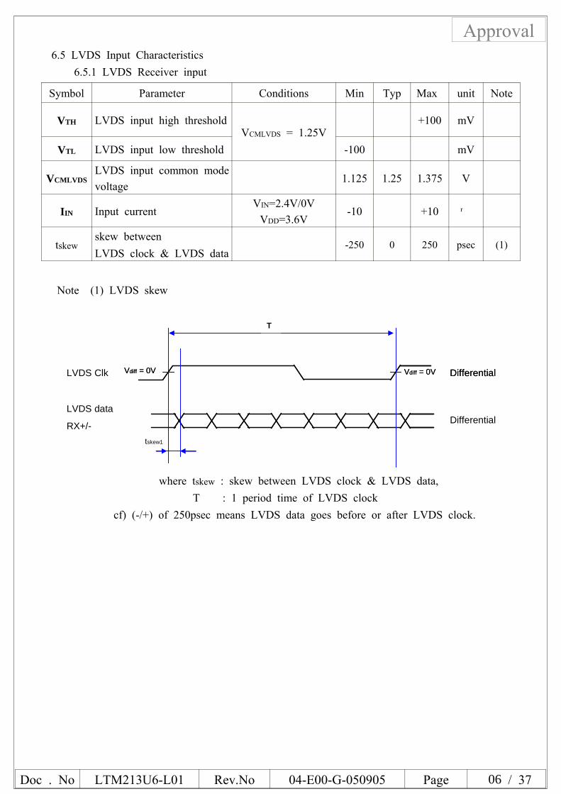
Approval6.5 LVDS Input Characteristics
6.5.1 LVDS Receiver input
Symbol Parameter Conditions Min Typ Max unit Note
VTH LVDS input high thresholdVCMLVDS = 1.25V
+100 mV
VTL LVDS input low threshold -100 mV
VCMLVDSLVDS input common modevoltage
1.125 1.25 1.375 V
IIN Input currentVIN=2.4V/0V
VDD=3.6V-10 +10
tskewskew betweenLVDS clock & LVDS data
-250 0 250 psec (1)
Note (1) LVDS skew
Vdiff = 0V
tskew1
Differential
Differential
LVDS Clk
LVDS data
RX+/-
T
Vdiff = 0VVdiff = 0V
tskew1
Differential
Differential
LVDS Clk
LVDS data
RX+/-
T
Vdiff = 0V
where tskew : skew between LVDS clock & LVDS data,T : 1 period time of LVDS clock
cf) (-/+) of 250psec means LVDS data goes before or after LVDS clock.
Doc . No LTM213U6-L01 Rev.No 04-E00-G-050905 Page 29 / 37
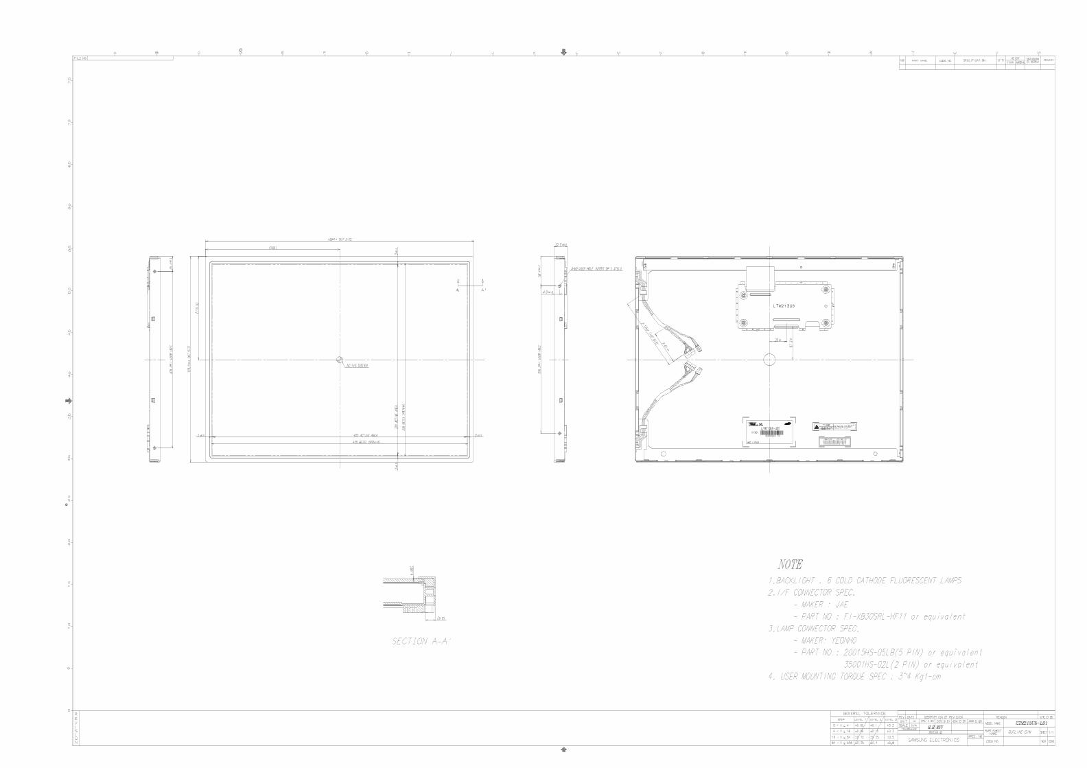
Approval7. Outline Dimension[ Refer to the next page ]
Doc . No LTM213U6-L01 Rev.No 04-E00-G-050905 Page 31 / 37
Approval
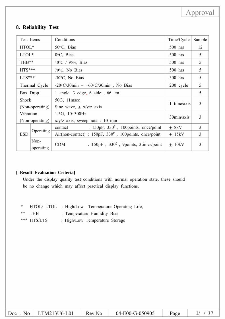
8. Reliability Test
Test Items Conditions Time/Cycle Sample
HTOL* 50°C, Bias 500 hrs 12
LTOL* 0°C, Bias 500 hrs 5
THB** 40°C / 95%, Bias 500 hrs 5
HTS*** 70°C, No Bias 500 hrs 5
LTS*** -30°C, No Bias 500 hrs 5
Thermal Cycle -20°C/30min ~ +60°C/30min , No Bias 200 cycle 5
Box Drop 1 angle, 3 edge, 6 side , 66 cm 5Shock(Non-operating)
50G, 11msecSine wave, ± x/y/z axis
1 time/axis 3
Vibration(Non-operating)
1.5G, 10~300Hzx/y/z axis, sweep rate : 10 min
30min/axis 3
ESDOperating
contact : 150pF, 330Ω, 100points, once/point ± 8kV 3Air(non-contact) : 150pF, 330Ω, 100points, once/point ± 15kV 3
Non-operating
CDM : 150pF , 330Ω, 9points, 3times/point ± 10kV 3
[ Result Evaluation Criteria]Under the display quality test conditions with normal operation state, these shouldbe no change which may affect practical display functions.
* HTOL/ LTOL : High/Low Temperature Operating Life,** THB : Temperature Humidity Bias*** HTS/LTS : High/Low Temperature Storage
Doc . No LTM213U6-L01 Rev.No 04-E00-G-050905 Page 32 / 37
Approval9. PACKING
9.1 CARTON (Internal Package)(1) Packing Form
EPS Cushion Pad(2) Packing Method
a) Without Inverter
NOTE) 1) TOTAL : Approx. 213±5%2) Cushion Material : EPS3) Cushion Size : 1,120(W) X 955(D) X 216(H)4) Packing Pallet Box Material : DW45) packing Pallet Box Size : 1,145(W) X 980(D) X 875(H)
Packing Pallet Box
Cushion Eps
Cushion Eps
Cushion Eps
Cushion EpsPallet Plastic
Module(28EA)
Module(28EA) 1st
layer
2nd
layer
Full-Packing State
PANEL-PROTECTOR
TAPE-PAPER(4 Point)
SHIELDING-BAG
EPS CUSHION
Before PALLET-Packing
Packing Flow
Doc . No LTM213U6-L01 Rev.No 04-E00-G-050905 Page 33 / 37
Approval(3) Packing Material
No ITEM Specification Remark
1LCD
Packing
28ea x 2 layer
= 56ea
(Packing-
Pallet Box)
1. LCD(56EA)
2. Cushion Eps(4ea)
3. Packing Pallet Box(1ea)
4. Cushion Material : EPS
5. Cushion Size : W1120 x D955 x H216
6. Packing Pallet Box Material : DW4
7. Packing Pallet Box Size : W1145 x D980 x H875
2 Pallet 1Box/Pallet1. Pallet Plastic(1ea)
2. Pallet Plastic Size : W1150 x D985 x H125
3Packing
DirectionVertical
10. MARKING & OTHERS
A nameplate bearing followed by is affixed to a shipped product at the specifiedlocation on each product.
(1) Parts number : LTM213U6-L01(2) Revision code : Two letters(3) Customer code : One letter
X XX
Revision CodeCustomer Code
(4) Lot number : 4 U 4 0 000000
Lot NumberMonthYearDeviceLine
(5) Nameplate Indication
Week Code : 0452
WeekYearLTM213U6-L01
Week
CodeLot Number XXX
15mm
50mm
Doc . No LTM213U6-L01 Rev.No 04-E00-G-050905 Page 34 / 37
Approval(6) Packing box attach
XXXParts NumberRevision Code
Box Serial Number
40mm
80mm
LTM213U6-L01
(7) Others1. After service part
Part Name Description
ASS'Y-LAMP(U)ASS'Y-LAMP(L)
LTM213U6, D2.4, L444.3, LJ91-00707A
LTM213U6, D2.4, L444.3, LJ91-00708A
Doc . No LTM213U6-L01 Rev.No 04-E00-G-050905 Page 35 / 37
Approval11. Inspection Criteria
When products are shipped, incoming inspection should be carried out with a samplinginspection based on MIL-STD-105E level II by AQL 1.0%.
CHANGE CONTROL
Design of the product may be changed regarding the specifications, appearance, parts used,circuits, etc. for product improvement.If a design change is judged to affect the specifications of this product, supplier shouldinform customer of the change in advance.
QUALITY CONTROL
In the event of a product failure under normal operating conditions, a product troubleor a functional disorder that can be deemed to be the responsibility of supplier, suppliershould repair the fault or replace the product free of charge within one year from theproduct delivery date. However, supplier does not take responsibility for the product qualityin the case of modifications not specified by supplier.
MAINTENANCE
The specifications of the functions of maintenance parts may be partially changedwithin the range which provides equivalent or better quality.In principle, maintenance parts should be product units.When stopping manufacturing this product, supplier should notify customer in advance.
HANDLING OF DOUBTFUL POINTS
Any doubt not stipulated in this specification is to be resolved by mutual agreementbetween customer and supplier, and supplier should make efforts for improvement in goodfaith.
Doc . No LTM213U6-L01 Rev.No 04-E00-G-050905 Page 36 / 37
Approval12. General Precautions
12.1 Handling
(a) When the module is assembled, it should be attached to the system firmlyusing all mounting holes. Be careful not to twist or bend the modules.
(b) Because the inverter uses high voltage, power should be disconnectedbefore it is assembled or disassembled.
(c) Refrain from strong mechanical shock and /or any force to the module.In addition to damage, this may cause improper operation or damage to the moduleand CCFT back-light.
(d) Note that polarizers are very fragile and could be easily damaged.Do not press or scratch the surface using the harder than a HB pencil lead.
(e) Wipe off water droplets or oil immediately.If you leave the droplets for a long time, staining and discoloration may occur.
(f) If the surface of the polarizer is dirty, clean it using some absorbent cotton orsoft cloth.
(g) The desirable cleaners are water, IPA(Isopropyl Alcohol) or Hexane.Do not use Ketone type materials(ex. Acetone), Ethyl alcohol, Toluene, Ethylacid or Methyl chloride. It might permanent damage to the polarizer due tochemical reaction.
(h) If the liquid crystal material leaks from the panel, it should be kept awayfrom the eyes or mouth. In case of contact with hands, legs or clothes, it mustbe washed away thoroughly with soap.
(i) Protect the module from static which may cause damage to the CMOS Gate Array IC.
(j) Use finger-stalls with soft gloves in order to keep display clean during theincoming inspection and assembly process.
(k) Do not disassemble the module.
(l) Do not pull or fold the lamp wire.
(m) Do not adjust the variable resistor located on the module.
(n) Protection film for polarizer on the module should be slowly peeled off just before useso that the electrostatic charge can be minimized.
(o) Pins of I/F connector should not be touched directly with bare hands.
Doc . No LTM213U6-L01 Rev.No 04-E00-G-050905 Page 37 / 37
Approval12.2 Storage
(a) Do not leave the module in high temperature, high humidity for a long time.It is highly recommended to store the module with temperature from 0 to 35 and relative humidity of less than 70%.
(b) Do not store the TFT-LCD module in direct sunlight.
(c) The module should be stored in a dark place.It is prohibited to apply sunlight or fluorescent light in storage.
12.3 Operation
(a) Do not connect or disconnect the module in the "Power On" condition.
(b) Power supply should always be turned on/off by 6.3 "Power on/off sequence"
(c) Module has high frequency circuits. Sufficient suppression to the electromagneticinterference should be done by system manufacturers. Grounding and shielding methodsmay be important to minimize the interference.
(d) The cable between the back-light connector and its inverter power supply shouldbe connected directly with a minimized length. A longer cable betweenthe back-light and the inverter may cause lower luminance of lamp(CCFT) andmay require higher startup voltage(Vs).
12.4 Others
(a) Ultra-violet ray filter is necessary for outdoor operation.
(b) Avoid condensation of water which may result in improper operation or disconnectionof electrode.
(c) Do not exceed the absolute maximum rating value. ( supply voltage variation,input voltage variation, variation in part contents and environmental temperature,and so on)Otherwise the module may be damaged.
(d) If the module keeps displaying the same pattern for a long period of time,the image may be "sticked" to the screen.To avoid image sticking, it is recommended to use a screen saver.
(e) This module has its circuitry PCB's on the rear side and should be handledcarefully in order not to be stressed.
(f) Please contact SEC in advance when you display the same pattern for a long time.
Recommended