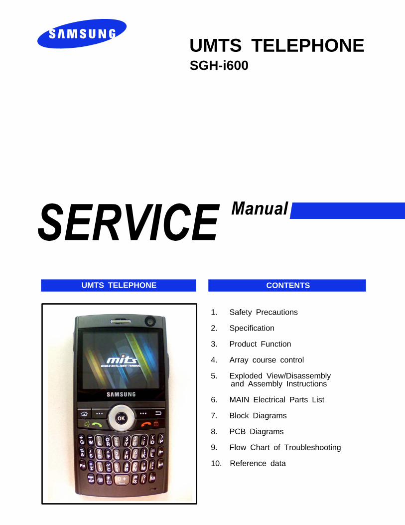
UMTS TELEPHONESGH-i600
UMTS TELEPHONE CONTENTS
1. Safety Precautions
2. Specification
3. Product Function
4. Array course control
5. Exploded View/Disassemblyand Assembly Instructions
6. MAIN Electrical Parts List
7. Block Diagrams
8. PCB Diagrams
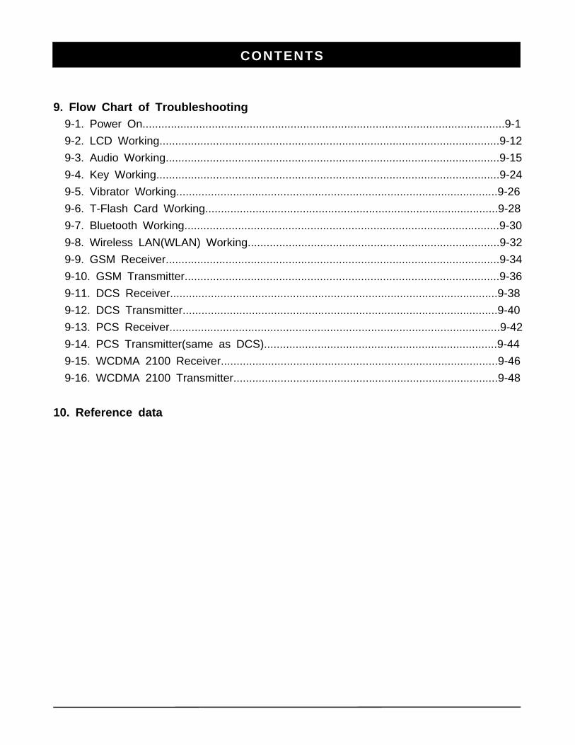
9. Flow Chart of Troubleshooting
10. Reference data
Samsung Electronics Co.,Ltd.
2006.12 Rev.1.0
ⓒThis Service Manual is a property of Samsung Electronics Co.,Ltd.Any unauthorized use of Manual can be punished under applicableInternational and/or domestic law.
CONTENTS
1. Safety Precautions1-1. Repair Precaution......................................................................................................1-11-2. ESD(Electrostatically Sensitive Devices) Precaution...............................................1-2
2. Specification2-1. GSM General Specification.......................................................................................2-12-2. GSM Tx Power Class...............................................................................................2-2
3. Product Function
4. Array course control4-1. Software Adjustments................................................................................................4-14-2. Software Downloading...............................................................................................4-3
5. Exploded View/Disassembly & Assembly Instructions5-1. Cellular phone Exploded View..................................................................................5-15-2. Cellular phone Parts list............................................................................................5-25-3. Disassembly & Assembly Instructions......................................................................5-4
6. MAIN Electrical Parts List
7. Block Diagrams7-1. RF Solution Block Diagram......................................................................................7-17-2. Base Band Solution Block Diagram.........................................................................7-2
8. PCB Diagrams
CONTENTS
9. Flow Chart of Troubleshooting9-1. Power On...................................................................................................................9-19-2. LCD Working............................................................................................................9-129-3. Audio Working..........................................................................................................9-159-4. Key Working.............................................................................................................9-249-5. Vibrator Working......................................................................................................9-269-6. T-Flash Card Working.............................................................................................9-289-7. Bluetooth Working....................................................................................................9-309-8. Wireless LAN(WLAN) Working................................................................................9-329-9. GSM Receiver..........................................................................................................9-349-10. GSM Transmitter....................................................................................................9-369-11. DCS Receiver........................................................................................................9-389-12. DCS Transmitter....................................................................................................9-409-13. PCS Receiver.........................................................................................................9-429-14. PCS Transmitter(same as DCS)..........................................................................9-449-15. WCDMA 2100 Receiver........................................................................................9-469-16. WCDMA 2100 Transmitter....................................................................................9-48
10. Reference data
SAMSUNG Proprietary-Contents may change without notice
1. Safety Precautions
1-1
This Document can not be used without Samsung's authorization
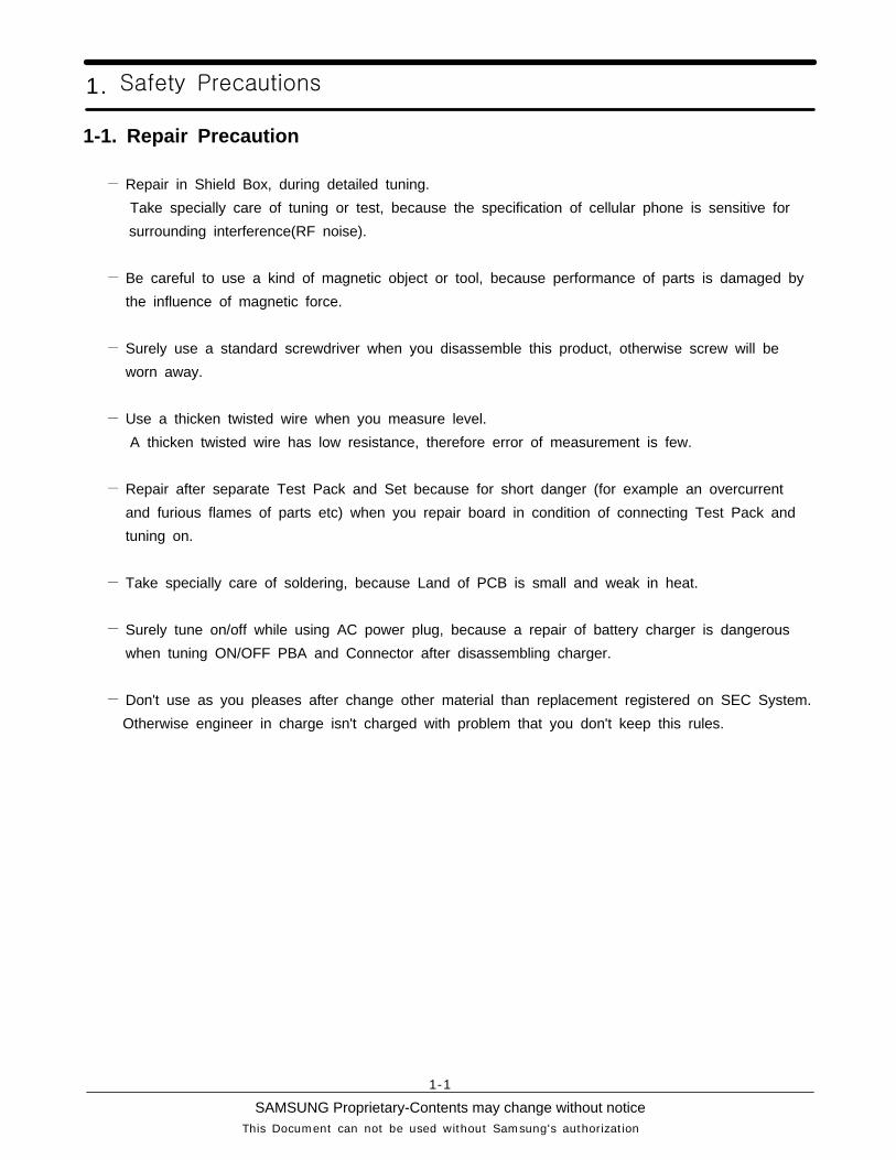
1-1. Repair Precaution
― Repair in Shield Box, during detailed tuning.Take specially care of tuning or test, because the specification of cellular phone is sensitive forsurrounding interference(RF noise).
― Be careful to use a kind of magnetic object or tool, because performance of parts is damaged bythe influence of magnetic force.
― Surely use a standard screwdriver when you disassemble this product, otherwise screw will beworn away.
― Use a thicken twisted wire when you measure level.A thicken twisted wire has low resistance, therefore error of measurement is few.
― Repair after separate Test Pack and Set because for short danger (for example an overcurrentand furious flames of parts etc) when you repair board in condition of connecting Test Pack andtuning on.
― Take specially care of soldering, because Land of PCB is small and weak in heat.
― Surely tune on/off while using AC power plug, because a repair of battery charger is dangerouswhen tuning ON/OFF PBA and Connector after disassembling charger.
― Don't use as you pleases after change other material than replacement registered on SEC System.Otherwise engineer in charge isn't charged with problem that you don't keep this rules.
SAMSUNG Proprietary-Contents may change without notice
Safety Precautions
1-2
This Document can not be used without Samsung's authorization
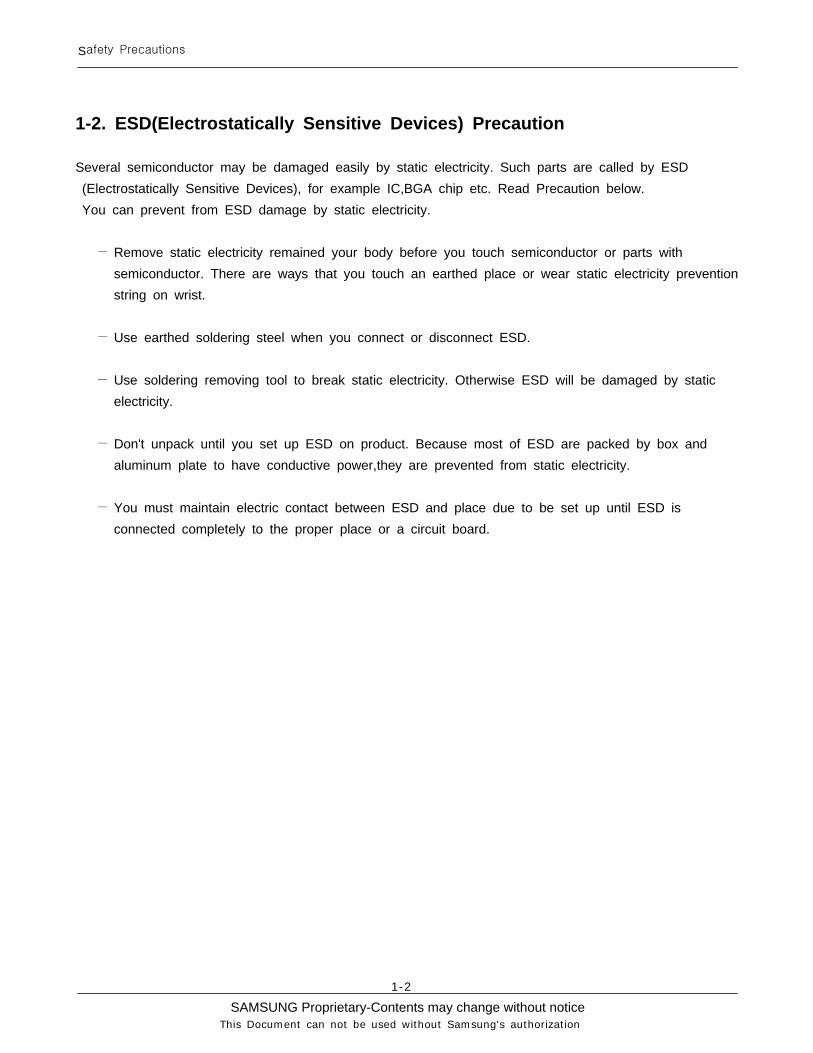
1-2. ESD(Electrostatically Sensitive Devices) Precaution
Several semiconductor may be damaged easily by static electricity. Such parts are called by ESD(Electrostatically Sensitive Devices), for example IC,BGA chip etc. Read Precaution below.You can prevent from ESD damage by static electricity.
― Remove static electricity remained your body before you touch semiconductor or parts withsemiconductor. There are ways that you touch an earthed place or wear static electricity preventionstring on wrist.
― Use earthed soldering steel when you connect or disconnect ESD.
― Use soldering removing tool to break static electricity. Otherwise ESD will be damaged by staticelectricity.
― Don't unpack until you set up ESD on product. Because most of ESD are packed by box andaluminum plate to have conductive power,they are prevented from static electricity.
― You must maintain electric contact between ESD and place due to be set up until ESD isconnected completely to the proper place or a circuit board.
SAMSUNG Proprietary-Contents may change without notice
2. Specification
This Document can not be used without Samsung's authorization
2-1
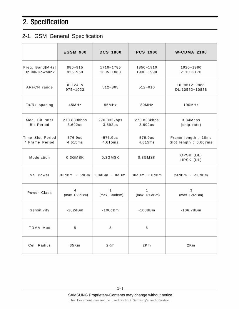
EGSM 900 DCS 1800 PCS 1900 W-CDMA 2100
Freq. Band[MHz]Upl ink/Downl ink
880~915925~960
1710~17851805~1880
1850~19101930~1990
1920~19802110~2170
ARFCN range0~124 &
975~1023512~885 512~810
UL:9612~9888DL:10562~10838
Tx/Rx spacing 45MHz 95MHz 80MHz 190MHz
Mod. Bit rate/Bi t Per iod
270.833kbps3.692us
270.833kbps3.692us
270.833kbps3.692us
3.84Mcps(chip rate)
Time Slot Per iod/ Frame Period
576.9us4.615ms
576.9us4.615ms
576.9us4.615ms
Frame length : 10msSlot length : 0.667ms
Modulat ion 0.3GMSK 0.3GMSK 0.3GMSKQPSK (DL)HPSK (UL)
MS Power 33dBm ~ 5dBm 30dBm ~ 0dBm 30dBm ~ 0dBm 24dBm ~ -50dBm
Power Class4
(max +33dBm)1
(max +30dBm)1
(max +30dBm)3
(max +24dBm)
Sensi t iv i ty -102dBm -100dBm -100dBm -106.7dBm
TDMA Mux 8 8 8
Cel l Radius 35Km 2Km 2Km 2Km
2-1. GSM General Specification
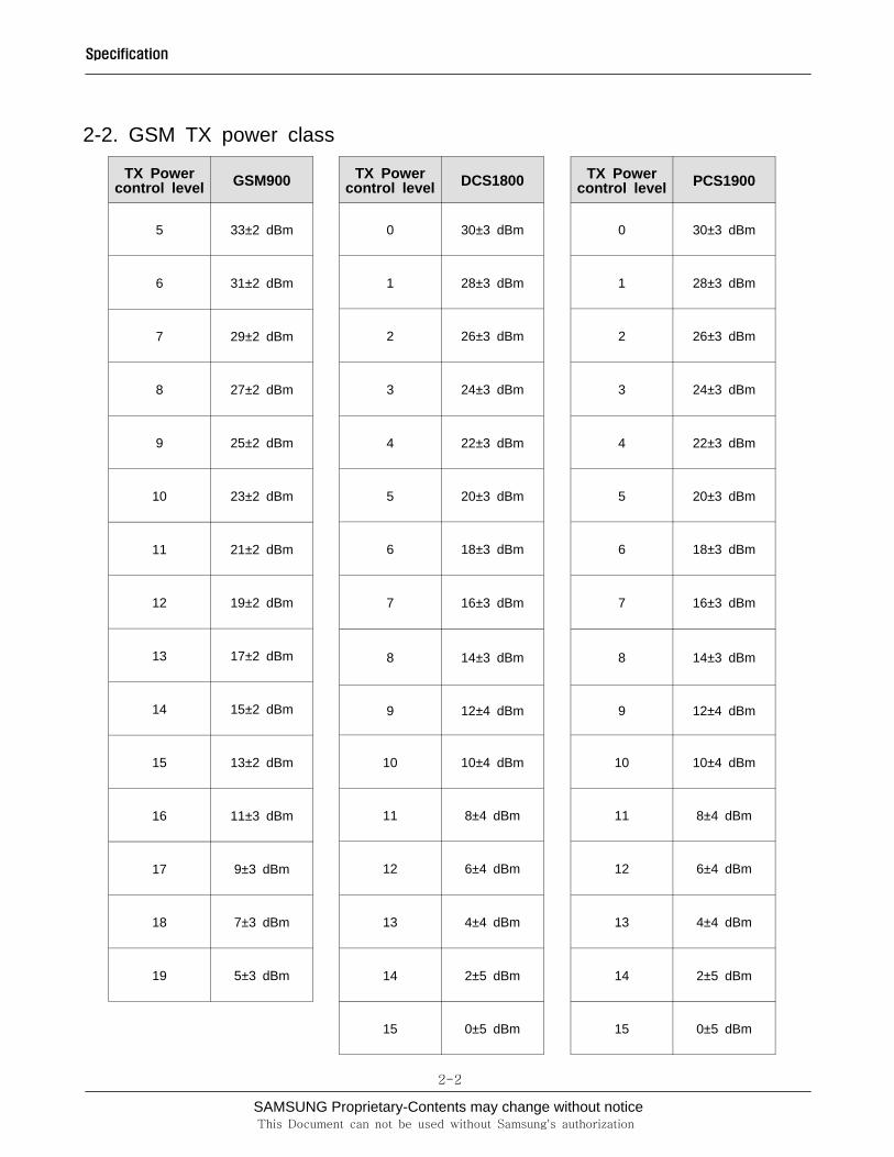
SAMSUNG Proprietary-Contents may change without noticeThis Document can not be used without Samsung's authorization
Specification
2-2
TX Powercontrol level PCS1900
0 30±3 dBm
1 28±3 dBm
2 26±3 dBm
3 24±3 dBm
4 22±3 dBm
5 20±3 dBm
6 18±3 dBm
7 16±3 dBm
8 14±3 dBm
9 12±4 dBm
10 10±4 dBm
11 8±4 dBm
12 6±4 dBm
13 4±4 dBm
14 2±5 dBm
15 0±5 dBm
TX Powercontrol level GSM900
5 33±2 dBm
6 31±2 dBm
7 29±2 dBm
8 27±2 dBm
9 25±2 dBm
10 23±2 dBm
11 21±2 dBm
12 19±2 dBm
13 17±2 dBm
14 15±2 dBm
15 13±2 dBm
16 11±3 dBm
17 9±3 dBm
18 7±3 dBm
19 5±3 dBm
TX Powercontrol level DCS1800
0 30±3 dBm
1 28±3 dBm
2 26±3 dBm
3 24±3 dBm
4 22±3 dBm
5 20±3 dBm
6 18±3 dBm
7 16±3 dBm
8 14±3 dBm
9 12±4 dBm
10 10±4 dBm
11 8±4 dBm
12 6±4 dBm
13 4±4 dBm
14 2±5 dBm
15 0±5 dBm
2-2. GSM TX power class
SAMSUNG Proprietary-Contents may change without notice
3. Product Function
3-1
This Document can not be used without Samsung's authorization
Main Function
― Homescreen - Card Wheel― PIM - Calendar, Contacts, Tasks, Voice Notes― Messaging - SMS, MMS, Postcard, E-Mail, Pocket MSN― Video Telephony― ActiveSync― Multimedia capability - Windows Media Player, Camera, Camcorder― Wireless capability - Bluetooth, Wireless LAN― Internet Explorer― Internet Sharing― Accessary Applications - Alarms, Calculator, D-Day, Notepad, Smart Converter,
Stopwatch, World Clock, Smart Search, Task Manager, OBEX FTP― RSS Reader, Podcast― Picsel Viewer― File Explorer, My Items― Voice Assist (only for germany, france, england, russia)― Speaker Phone capability― Games (Bubble Breaker, Solitaire)

SAMSUNG Proprietary-Contents may change without notice
Product Function
3-2
This Document can not be used without Samsung's authorization
SAMSUNG Proprietary-Contents may change without notice
4. Array course control
4-1
This Document can not be used without Samsung's authorization
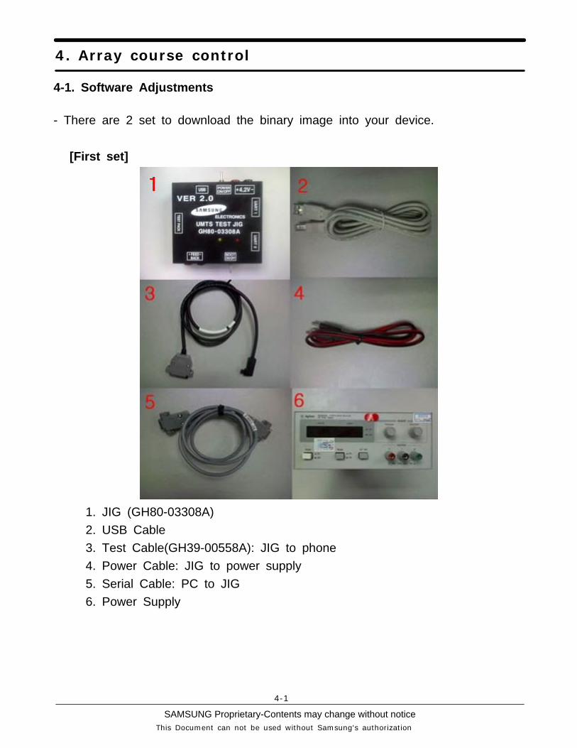
4-1. Software Adjustments
- There are 2 set to download the binary image into your device.
[First set]
1. JIG (GH80-03308A)2. USB Cable3. Test Cable(GH39-00558A): JIG to phone4. Power Cable: JIG to power supply5. Serial Cable: PC to JIG6. Power Supply
SAMSUNG Proprietary-Contents may change without notice
Array course control
4-2
This Document can not be used without Samsung's authorization
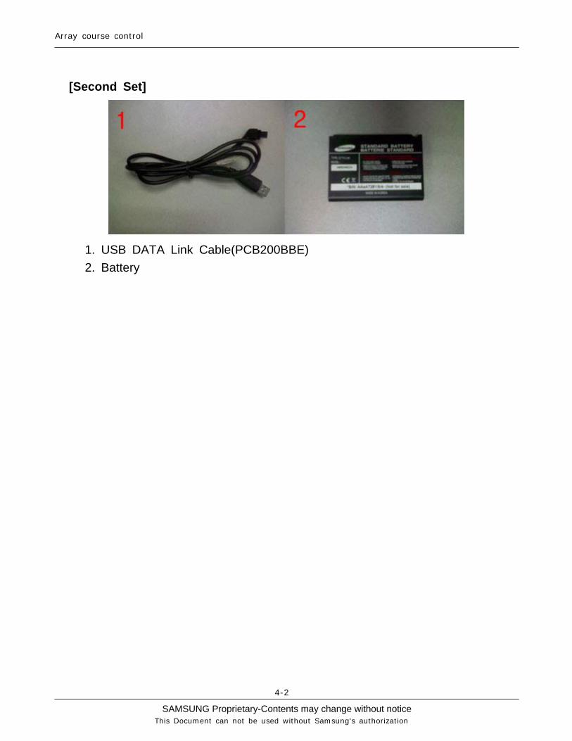
[Second Set]
1. USB DATA Link Cable(PCB200BBE)2. Battery
SAMSUNG Proprietary-Contents may change without notice
Array course control
4-3
This Document can not be used without Samsung's authorization
4-2. Software Download
4-2-1. Pre-requisite for Download
• Downloader Program (there are 3 ways to download.)
- WCEDownloader v1.1Single.exe
- WCEDownloader v1.1.exe (multidownloader)
- [unknown].exe
• SGH_I600 Mobile Device• Binary files• Active sync Setting
• Driver Installation.
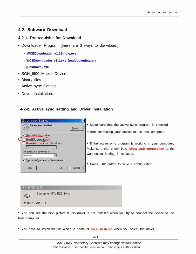
4-2-2. Active sync setting and Driver Installation
• Make sure that the active sync program is checked
before connecting your device to the host computer.
• If the active sync program is working in your computer,Make sure that check box, Allow USB connection at theConnection Setting, is released.
• Press ‘OK’ button to save a configuration.
• You can see the next picture if usb driver is not installed when you try to connect the device to thehost computer.
• You have to install the file which is name of ‘wceusbsh.inf’ when you select the driver.
SAMSUNG Proprietary-Contents may change without notice
Array course control
4-4
This Document can not be used without Samsung's authorization
4-2-3. S/W Download Process
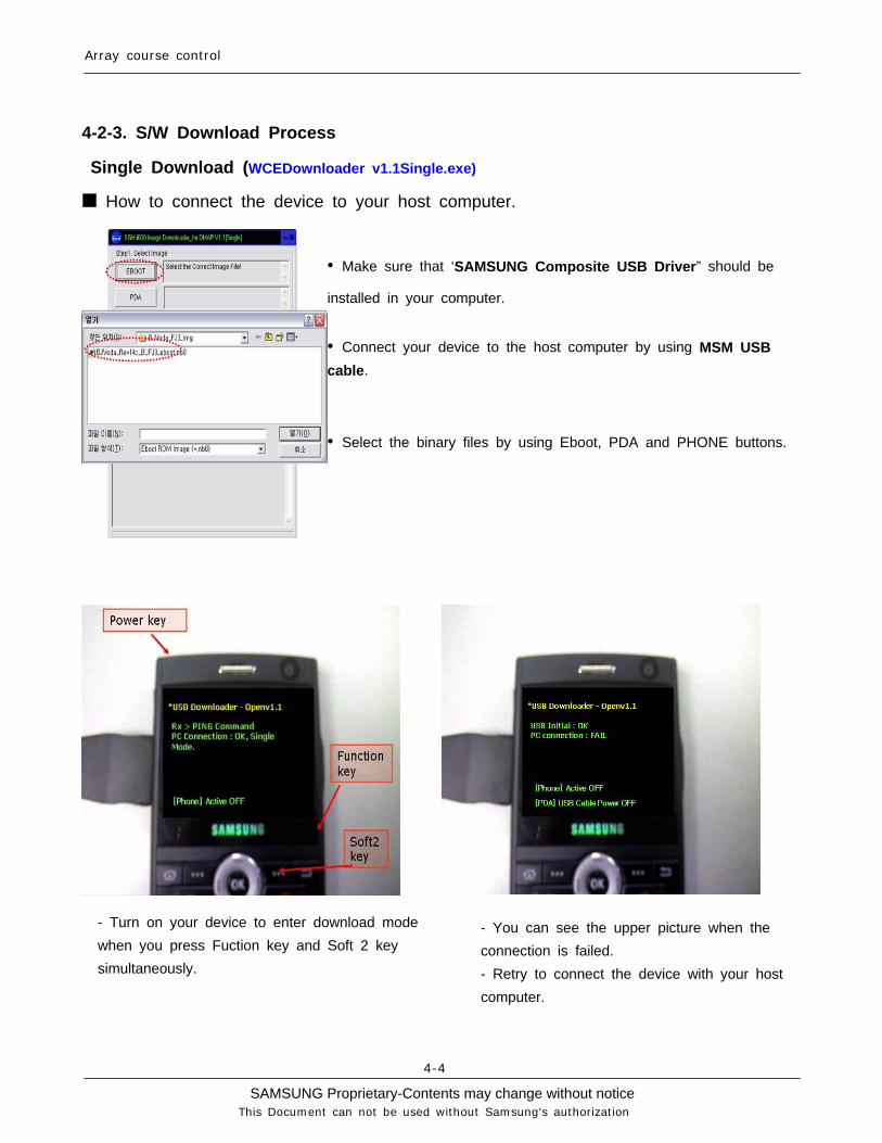
Single Download (WCEDownloader v1.1Single.exe)
■ How to connect the device to your host computer.
• Make sure that ‘SAMSUNG Composite USB Driver” should be
installed in your computer.
• Connect your device to the host computer by using MSM USBcable.
• Select the binary files by using Eboot, PDA and PHONE buttons.
- Turn on your device to enter download modewhen you press Fuction key and Soft 2 keysimultaneously.
- You can see the upper picture when theconnection is failed.- Retry to connect the device with your hostcomputer.
SAMSUNG Proprietary-Contents may change without notice
Array course control
4-5
This Document can not be used without Samsung's authorization
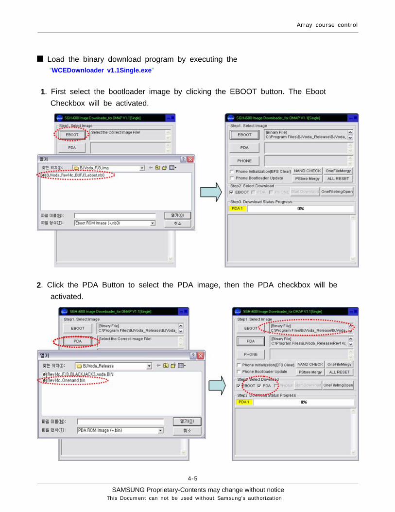
■ Load the binary download program by executing the“WCEDownloader v1.1Single.exe”
1. First select the bootloader image by clicking the EBOOT button. The EbootCheckbox will be activated.
2. Click the PDA Button to select the PDA image, then the PDA checkbox will beactivated.
SAMSUNG Proprietary-Contents may change without notice
Array course control
4-6
This Document can not be used without Samsung's authorization
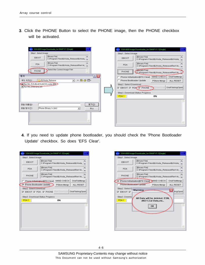
3. Click the PHONE Button to select the PHONE image, then the PHONE checkboxwill be activated.
4. If you need to update phone bootloader, you should check the 'Phone BootloaderUpdate' checkbox. So does 'EFS Clear'.
SAMSUNG Proprietary-Contents may change without notice
Array course control
4-7
This Document can not be used without Samsung's authorization
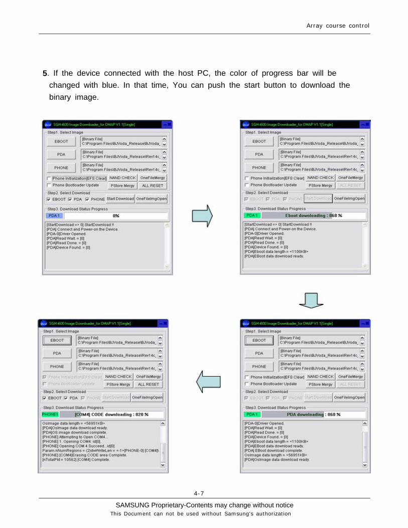
5. If the device connected with the host PC, the color of progress bar will bechanged with blue. In that time, You can push the start button to download thebinary image.
SAMSUNG Proprietary-Contents may change without notice
Array course control
4-8
This Document can not be used without Samsung's authorization
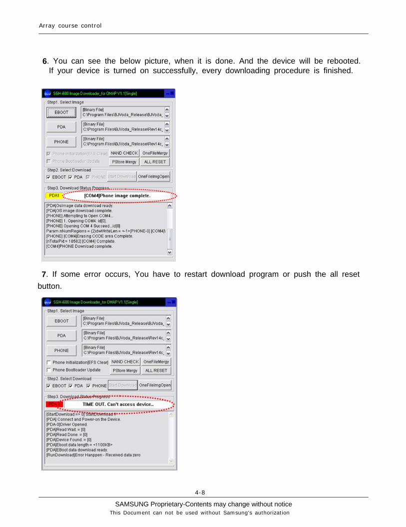
6. You can see the below picture, when it is done. And the device will be rebooted.If your device is turned on successfully, every downloading procedure is finished.
7. If some error occurs, You have to restart download program or push the all resetbutton.
SAMSUNG Proprietary-Contents may change without notice
Array course control
4-9
This Document can not be used without Samsung's authorization
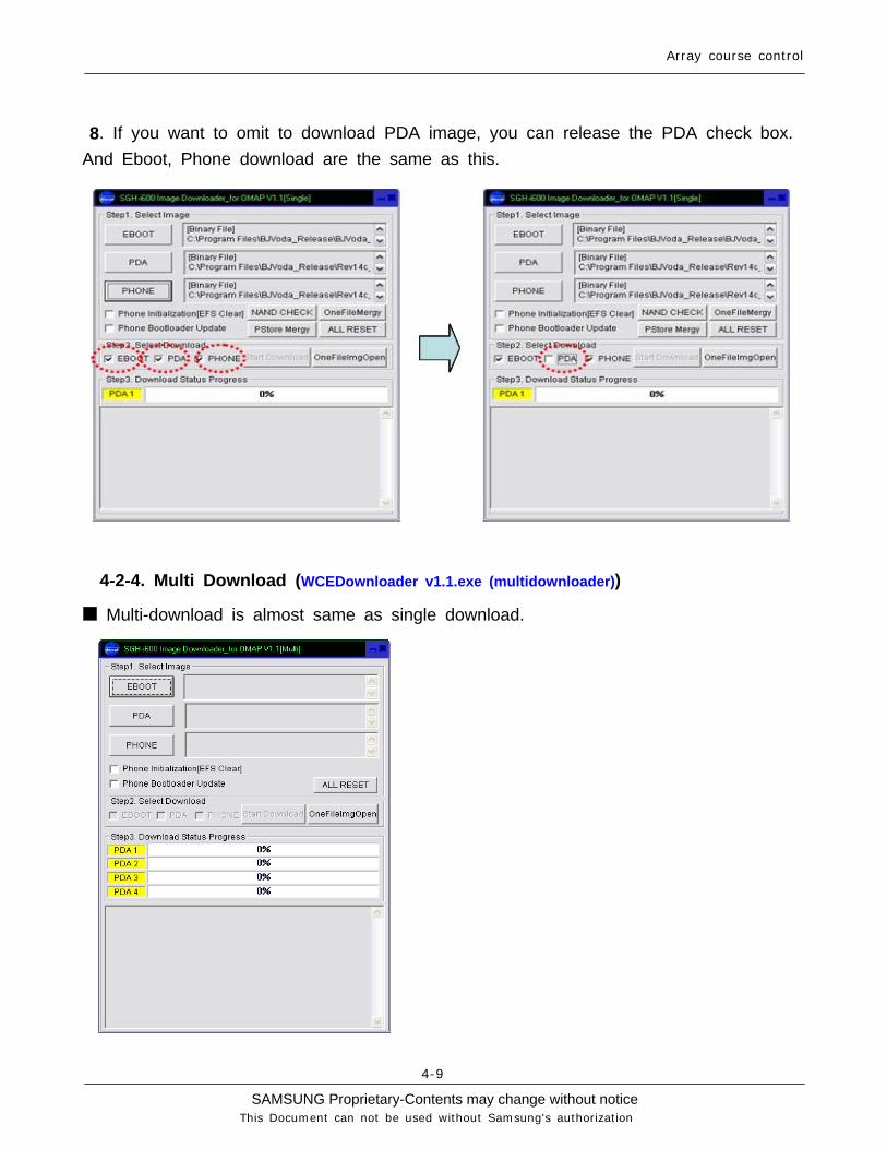
8. If you want to omit to download PDA image, you can release the PDA check box.And Eboot, Phone download are the same as this.
4-2-4. Multi Download (WCEDownloader v1.1.exe (multidownloader))
■ Multi-download is almost same as single download.
SAMSUNG Proprietary-Contents may change without notice
Array course control
4-10
This Document can not be used without Samsung's authorization
■ The difference is below.
1. There are four progress bars. It means you can download four devices at
once.
2. The device will be rebooted automatically after download. In that time,
'MITs USB RNDIS Driver' is not detected in the host PC. It means you can't
use the active sync program. So Make sure that you have to restart the
device after first booting.
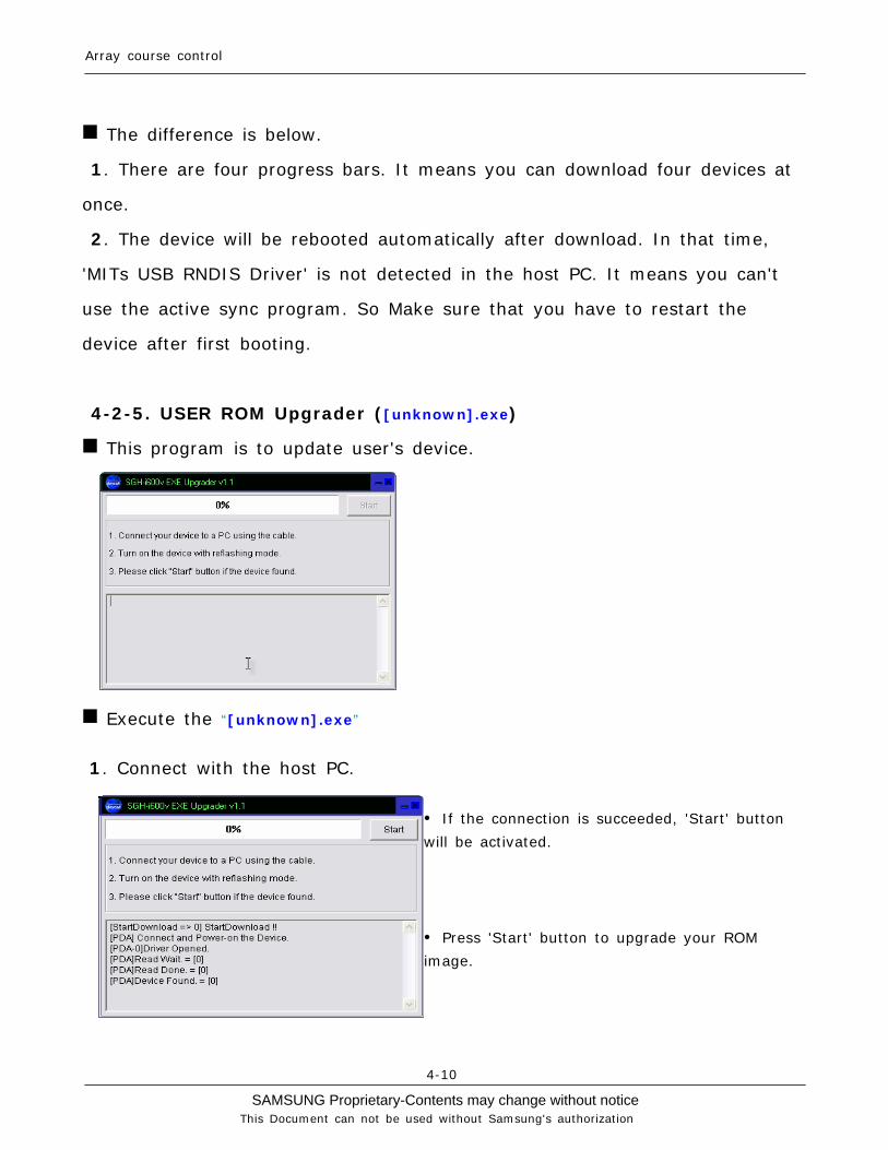
4-2-5. USER ROM Upgrader ([unknown].exe)
■ This program is to update user's device.
■ Execute the “[unknown].exe”
1. Connect with the host PC.
• If the connection is succeeded, 'Start' button
will be activated.
• Press 'Start' button to upgrade your ROM
image.
SAMSUNG Proprietary-Contents may change without notice
Array course control
4-11
This Document can not be used without Samsung's authorization
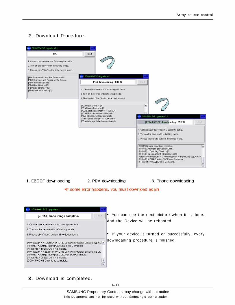
2. Download Procedure
• You can see the next picture when it is done.
And the Device will be rebooted.
• If your device is turned on successfully, every
downloading procedure is finished.
3. Download is completed.
SAMSUNG Proprietary-Contents may change without notice
Array course control
4-12
This Document can not be used without Samsung's authorization
SAMSUNG Proprietary-Contents may change without notice
5-3
This Document can not be used without Samsung's authorization
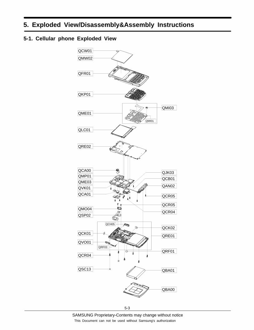
5. Exploded View/Disassembly&Assembly Instructions
5-1. Cellular phone Exploded View
QMW02
QMI03
QMI01
QCH05
QFR01
QCW01
QME01
QLC01
QRE02
QCA00
QME03QMP01
QVK01QCA01
QMO04QSP02
QKP01
QCK01
QVO01
QCR04
QSC13
QCR04
QAN02
QCR05
QCR05
QRE01
QRF01
QBA00
QBA01
QCK02
QCB01QJK03
QRF03
SAMSUNG Proprietary-Contents may change without notice
Exploded View/Disassembly&Assembly Instructions
5-2
This Document can not be used without Samsung's authorization
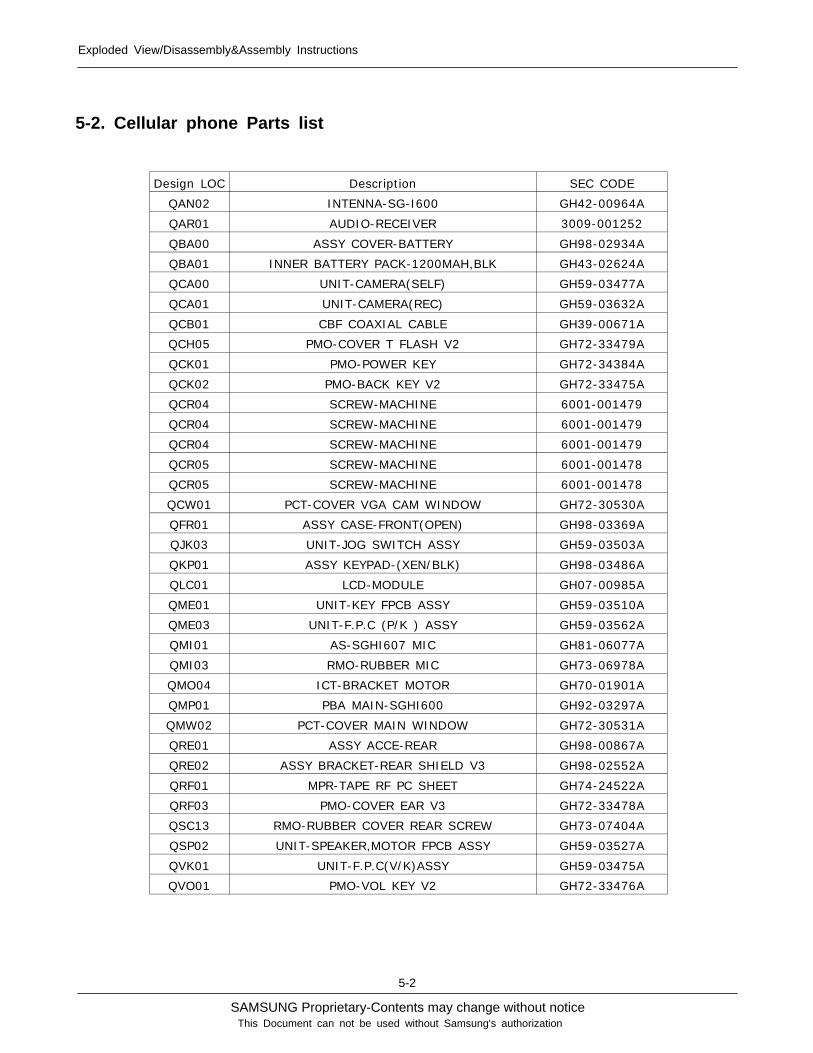
5-2. Cellular phone Parts list
Design LOC Description SEC CODE
QAN02 INTENNA-SG-I600 GH42-00964A
QAR01 AUDIO-RECEIVER 3009-001252
QBA00 ASSY COVER-BATTERY GH98-02934A
QBA01 INNER BATTERY PACK-1200MAH,BLK GH43-02624A
QCA00 UNIT-CAMERA(SELF) GH59-03477A
QCA01 UNIT-CAMERA(REC) GH59-03632A
QCB01 CBF COAXIAL CABLE GH39-00671A
QCH05 PMO-COVER T FLASH V2 GH72-33479A
QCK01 PMO-POWER KEY GH72-34384A
QCK02 PMO-BACK KEY V2 GH72-33475A
QCR04 SCREW-MACHINE 6001-001479
QCR04 SCREW-MACHINE 6001-001479
QCR04 SCREW-MACHINE 6001-001479
QCR05 SCREW-MACHINE 6001-001478
QCR05 SCREW-MACHINE 6001-001478
QCW01 PCT-COVER VGA CAM WINDOW GH72-30530A
QFR01 ASSY CASE-FRONT(OPEN) GH98-03369A
QJK03 UNIT-JOG SWITCH ASSY GH59-03503A
QKP01 ASSY KEYPAD-(XEN/BLK) GH98-03486A
QLC01 LCD-MODULE GH07-00985A
QME01 UNIT-KEY FPCB ASSY GH59-03510A
QME03 UNIT-F.P.C (P/K ) ASSY GH59-03562A
QMI01 AS-SGHI607 MIC GH81-06077A
QMI03 RMO-RUBBER MIC GH73-06978A
QMO04 ICT-BRACKET MOTOR GH70-01901A
QMP01 PBA MAIN-SGHI600 GH92-03297A
QMW02 PCT-COVER MAIN WINDOW GH72-30531A
QRE01 ASSY ACCE-REAR GH98-00867A
QRE02 ASSY BRACKET-REAR SHIELD V3 GH98-02552A
QRF01 MPR-TAPE RF PC SHEET GH74-24522A
QRF03 PMO-COVER EAR V3 GH72-33478A
QSC13 RMO-RUBBER COVER REAR SCREW GH73-07404A
QSP02 UNIT-SPEAKER,MOTOR FPCB ASSY GH59-03527A
QVK01 UNIT-F.P.C(V/K)ASSY GH59-03475A
QVO01 PMO-VOL KEY V2 GH72-33476A
SAMSUNG Proprietary-Contents may change without notice
Exploded View/Disassembly&Assembly Instructions
5-3
This Document can not be used without Samsung's authorization
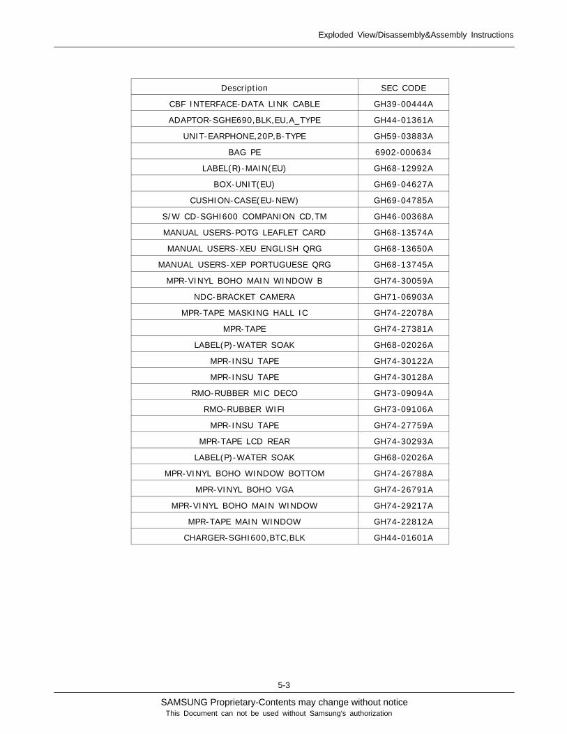
Description SEC CODE
CBF INTERFACE-DATA LINK CABLE GH39-00444A
ADAPTOR-SGHE690,BLK,EU,A_TYPE GH44-01361A
UNIT-EARPHONE,20P,B-TYPE GH59-03883A
BAG PE 6902-000634
LABEL(R)-MAIN(EU) GH68-12992A
BOX-UNIT(EU) GH69-04627A
CUSHION-CASE(EU-NEW) GH69-04785A
S/W CD-SGHI600 COMPANION CD,TM GH46-00368A
MANUAL USERS-POTG LEAFLET CARD GH68-13574A
MANUAL USERS-XEU ENGLISH QRG GH68-13650A
MANUAL USERS-XEP PORTUGUESE QRG GH68-13745A
MPR-VINYL BOHO MAIN WINDOW B GH74-30059A
NDC-BRACKET CAMERA GH71-06903A
MPR-TAPE MASKING HALL IC GH74-22078A
MPR-TAPE GH74-27381A
LABEL(P)-WATER SOAK GH68-02026A
MPR-INSU TAPE GH74-30122A
MPR-INSU TAPE GH74-30128A
RMO-RUBBER MIC DECO GH73-09094A
RMO-RUBBER WIFI GH73-09106A
MPR-INSU TAPE GH74-27759A
MPR-TAPE LCD REAR GH74-30293A
LABEL(P)-WATER SOAK GH68-02026A
MPR-VINYL BOHO WINDOW BOTTOM GH74-26788A
MPR-VINYL BOHO VGA GH74-26791A
MPR-VINYL BOHO MAIN WINDOW GH74-29217A
MPR-TAPE MAIN WINDOW GH74-22812A
CHARGER-SGHI600,BTC,BLK GH44-01601A
SAMSUNG Proprietary-Contents may change without notice
Exploded View/Disassembly&Assembly Instructions
5-4
This Document can not be used without Samsung's authorization
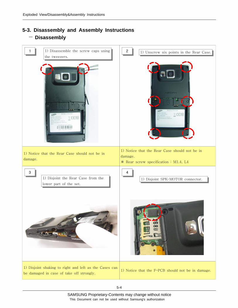
1) Notice that the Rear Case should not be in
damage.
1) Notice that the Rear Case should not be in
damage.
※ Rear screw specification : M1.4, L4
1) Disjoint shaking to right and left as the Cases can
be damaged in case of take off strongly.1) Notice that the F-PCB should not be in damage.
1 2
3 4
1) Unscrew six points in the Rear Case.1) Disassemble the screw caps using
the tweezers.
1) Disjoint the Rear Case from the
lower part of the set.
1) Disjoint SPK-MOTOR connector.
5-3. Disassembly and Assembly Instructions― Disassembly
SAMSUNG Proprietary-Contents may change without notice
Exploded View/Disassembly&Assembly Instructions
5-5
This Document can not be used without Samsung's authorization
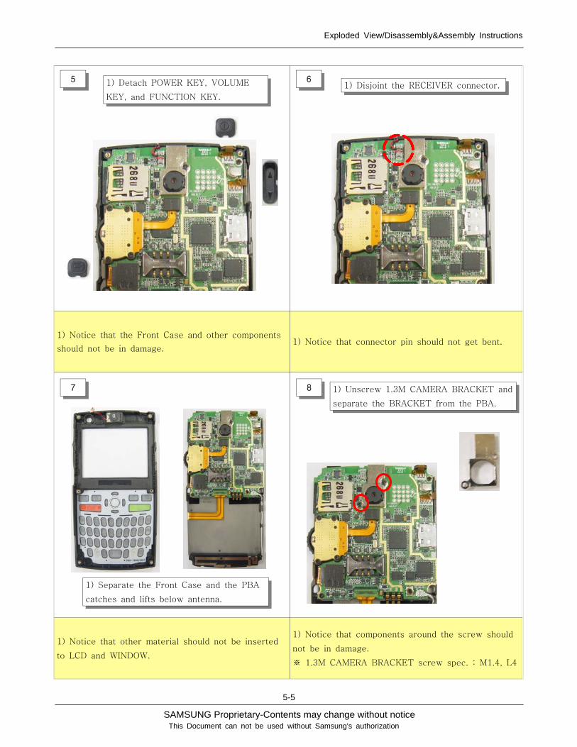
1) Notice that the Front Case and other components
should not be in damage.1) Notice that connector pin should not get bent.
1) Notice that other material should not be inserted
to LCD and WINDOW.
1) Notice that components around the screw should
not be in damage.
※ 1.3M CAMERA BRACKET screw spec. : M1.4, L4
5 6
7 8
1) Detach POWER KEY, VOLUME
KEY, and FUNCTION KEY.
1) Disjoint the RECEIVER connector.
1) Separate the Front Case and the PBA
catches and lifts below antenna.
1) Unscrew 1.3M CAMERA BRACKET and
separate the BRACKET from the PBA.
SAMSUNG Proprietary-Contents may change without notice
Exploded View/Disassembly&Assembly Instructions
5-6
This Document can not be used without Samsung's authorization
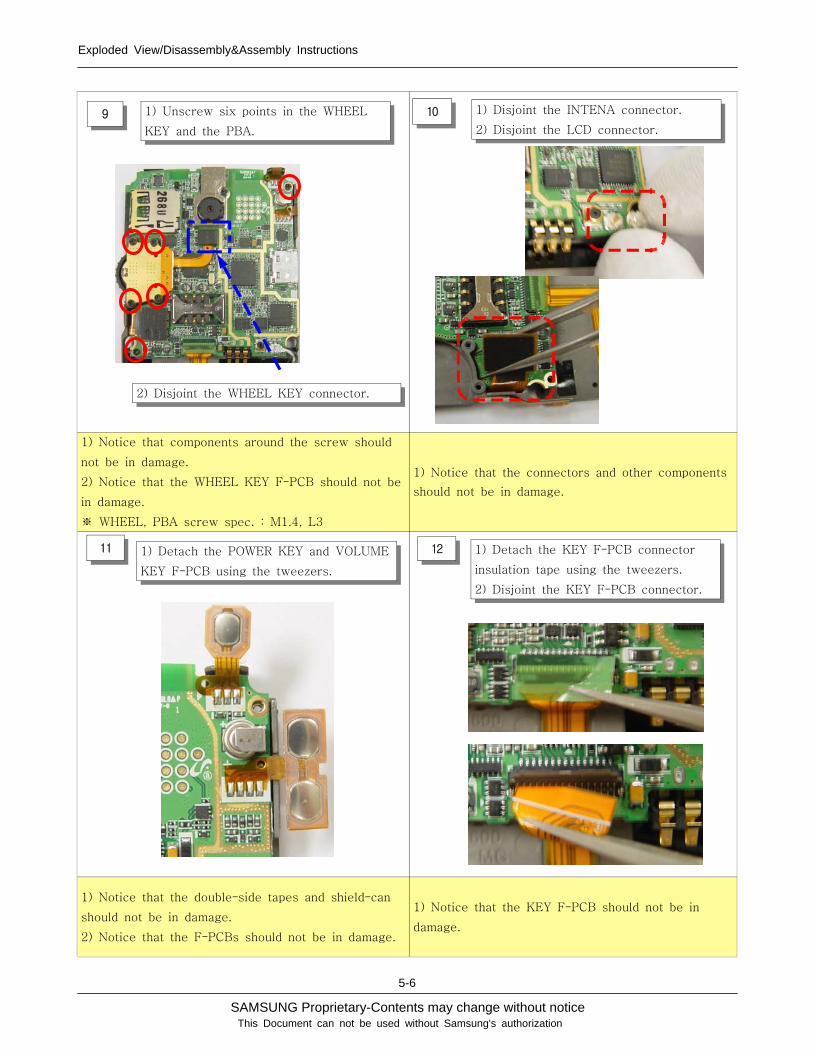
1) Notice that components around the screw should
not be in damage.
2) Notice that the WHEEL KEY F-PCB should not be
in damage.
※ WHEEL, PBA screw spec. : M1.4, L3
1) Notice that the connectors and other components
should not be in damage.
1) Notice that the double-side tapes and shield-can
should not be in damage.
2) Notice that the F-PCBs should not be in damage.
1) Notice that the KEY F-PCB should not be in
damage.
9 10
11 12
1) Unscrew six points in the WHEEL
KEY and the PBA.
2) Disjoint the WHEEL KEY connector.
1) Disjoint the INTENA connector.
2) Disjoint the LCD connector.
1) Detach the POWER KEY and VOLUME
KEY F-PCB using the tweezers.
1) Detach the KEY F-PCB connector
insulation tape using the tweezers.
2) Disjoint the KEY F-PCB connector.
SAMSUNG Proprietary-Contents may change without notice
Exploded View/Disassembly&Assembly Instructions
5-7
This Document can not be used without Samsung's authorization
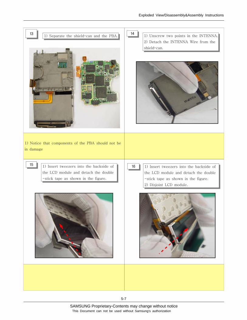
1) Notice that components of the PBA should not be
in damage
131) Separate the shield-can and the PBA. 1) Unscrew two points in the INTENNA.
2) Detach the INTENNA Wire from the
shield-can.
14
1) Insert tweezers into the backside of
the LCD module and detach the double
-stick tape as shown in the figure.
1) Insert tweezers into the backside of
the LCD module and detach the double
-stick tape as shown in the figure.
2) Disjoint LCD module.
15 16
SAMSUNG Proprietary-Contents may change without notice
Exploded View/Disassembly&Assembly Instructions
5-8
This Document can not be used without Samsung's authorization
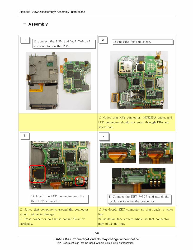
1) Notice that KEY connector, INTENNA cable, and
LCD connector should not enter through PBA and
shield-can.
1) Notice that components around the connector
should not be in damage.
2) Press connector so that is sonant 'Exactly'
vertically.
1) Put deeply KEY connector so that reach to white
line.
2) Insulation tape covers whole so that connector
may not come out.
1 1) Connect the 1.3M and VGA CAMERA
to connector on the PBA.
21) Put PBA for shield-can.
3 4
1) Connect the KEY F-PCB and attach the
insulation tape on the connector.
1) Attach the LCD connector and the
INTENNA connector.
― Assembly
SAMSUNG Proprietary-Contents may change without notice
Exploded View/Disassembly&Assembly Instructions
5-9
This Document can not be used without Samsung's authorization
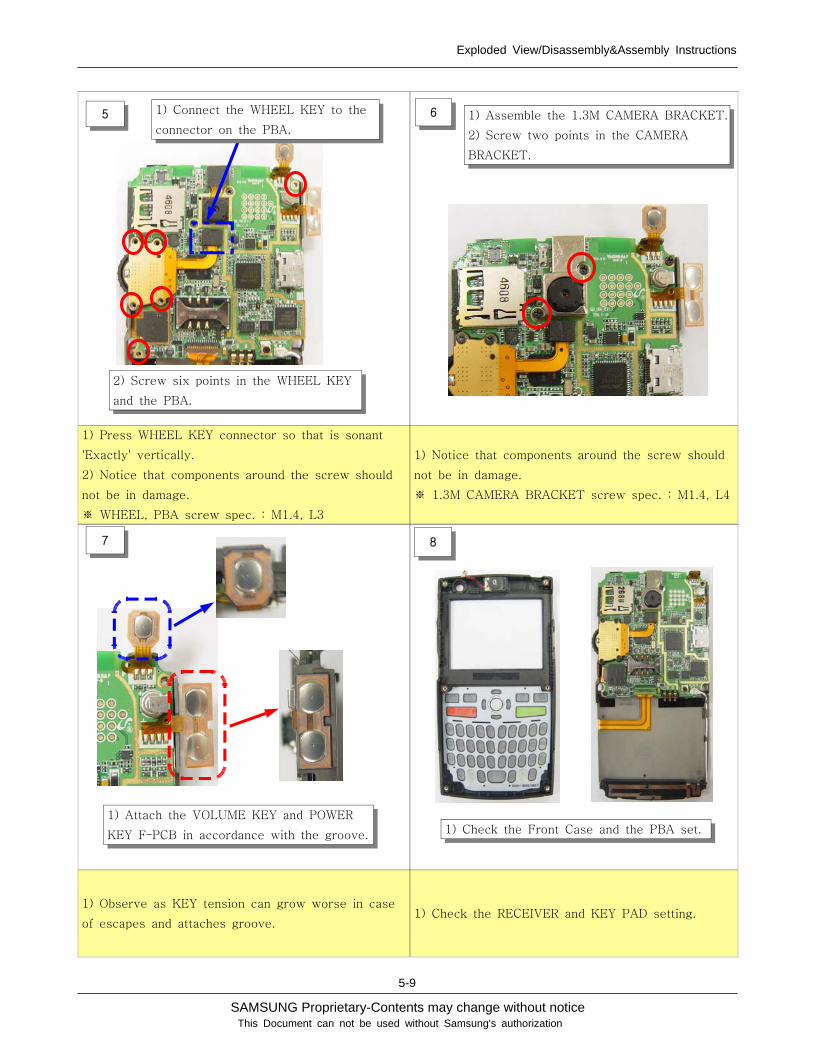
1) Press WHEEL KEY connector so that is sonant
'Exactly' vertically.
2) Notice that components around the screw should
not be in damage.
※ WHEEL, PBA screw spec. : M1.4, L3
1) Notice that components around the screw should
not be in damage.
※ 1.3M CAMERA BRACKET screw spec. : M1.4, L4
1) Observe as KEY tension can grow worse in case
of escapes and attaches groove.1) Check the RECEIVER and KEY PAD setting.
1) Attach the VOLUME KEY and POWER
KEY F-PCB in accordance with the groove.
8
65
7
2) Screw six points in the WHEEL KEY
and the PBA.
1) Connect the WHEEL KEY to the
connector on the PBA.1) Assemble the 1.3M CAMERA BRACKET.
2) Screw two points in the CAMERA
BRACKET.
1) Check the Front Case and the PBA set.
SAMSUNG Proprietary-Contents may change without notice
Exploded View/Disassembly&Assembly Instructions
5-10
This Document can not be used without Samsung's authorization
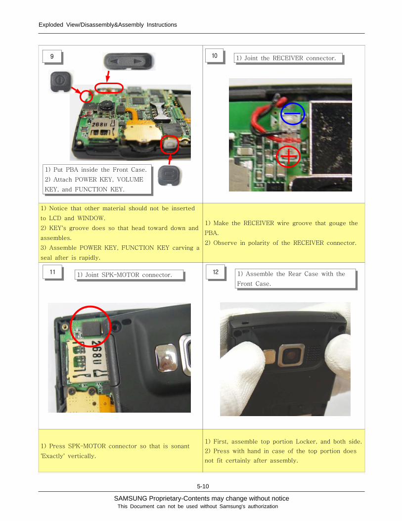
1) Notice that other material should not be inserted
to LCD and WINDOW.
2) KEY's groove does so that head toward down and
assembles.
3) Assemble POWER KEY, FUNCTION KEY carving a
seal after is rapidly.
1) Make the RECEIVER wire groove that gouge the
PBA.
2) Observe in polarity of the RECEIVER connector.
1) Press SPK-MOTOR connector so that is sonant
'Exactly' vertically.
1) First, assemble top portion Locker, and both side.
2) Press with hand in case of the top portion does
not fit certainly after assembly.
12
109
11
1) Put PBA inside the Front Case.
2) Attach POWER KEY, VOLUME
KEY, and FUNCTION KEY.
1) Joint the RECEIVER connector.
1) Joint SPK-MOTOR connector. 1) Assemble the Rear Case with the
Front Case.
SAMSUNG Proprietary-Contents may change without notice
Exploded View/Disassembly&Assembly Instructions
5-11
This Document can not be used without Samsung's authorization
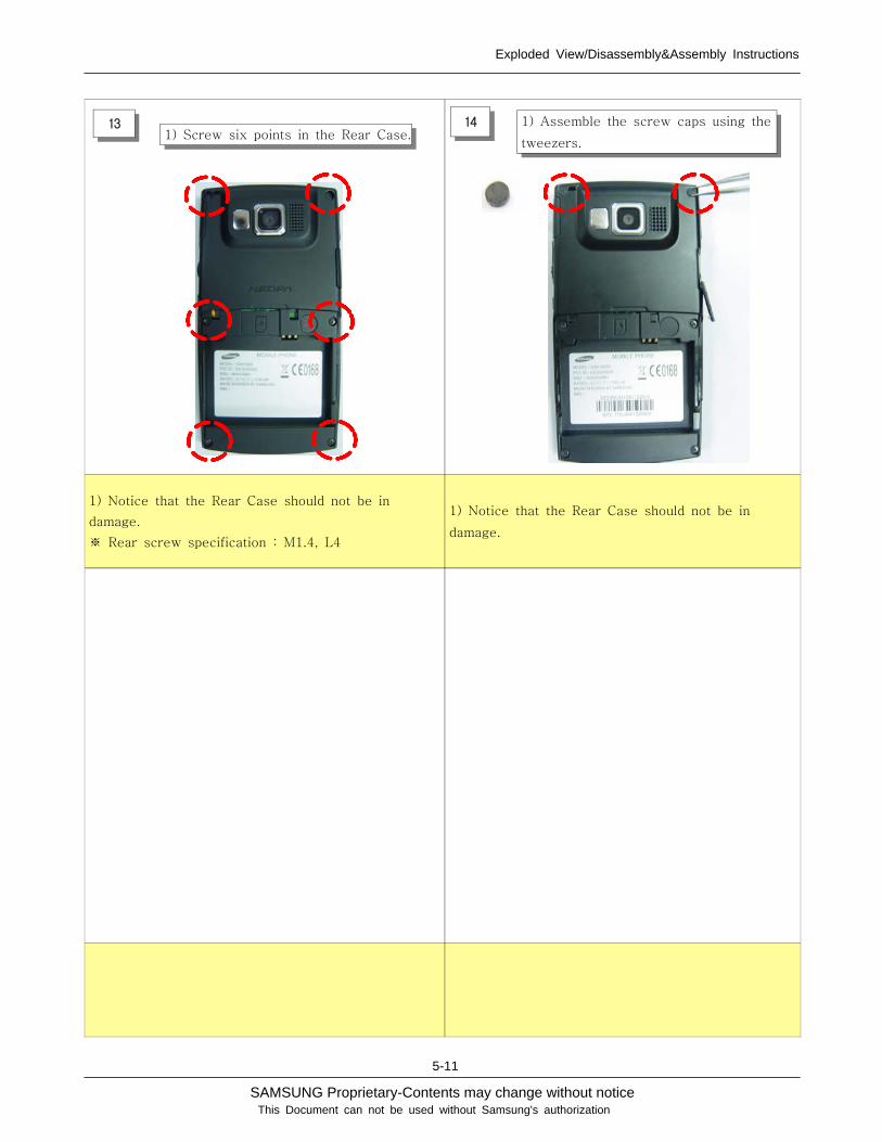
1) Notice that the Rear Case should not be in
damage.
※ Rear screw specification : M1.4, L4
1) Notice that the Rear Case should not be in
damage.
14131) Screw six points in the Rear Case.
1) Assemble the screw caps using the
tweezers.
SAMSUNG Proprietary-Contents may change without notice
Exploded View/Disassembly&Assembly Instructions
5-12
This Document can not be used without Samsung's authorization
SAMSUNG Proprietary-Contents may change without notice
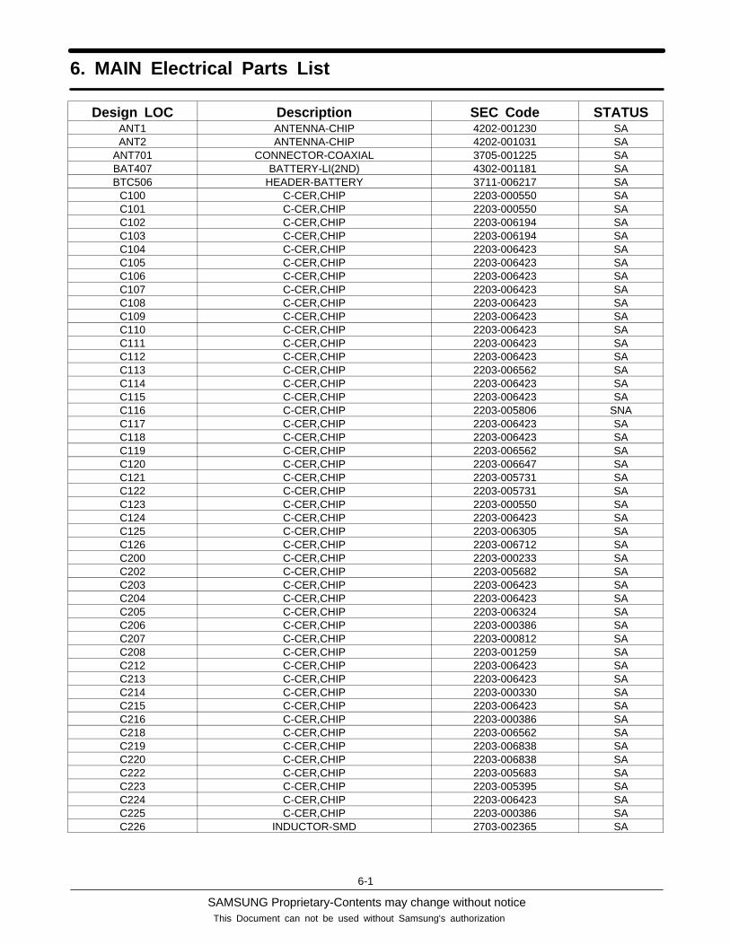
6. MAIN Electrical Parts List
6-1
This Document can not be used without Samsung's authorization
Design LOC Description SEC Code STATUSANT1 ANTENNA-CHIP 4202-001230 SAANT2 ANTENNA-CHIP 4202-001031 SA
ANT701 CONNECTOR-COAXIAL 3705-001225 SABAT407 BATTERY-LI(2ND) 4302-001181 SABTC506 HEADER-BATTERY 3711-006217 SA
C100 C-CER,CHIP 2203-000550 SAC101 C-CER,CHIP 2203-000550 SAC102 C-CER,CHIP 2203-006194 SAC103 C-CER,CHIP 2203-006194 SAC104 C-CER,CHIP 2203-006423 SAC105 C-CER,CHIP 2203-006423 SAC106 C-CER,CHIP 2203-006423 SAC107 C-CER,CHIP 2203-006423 SAC108 C-CER,CHIP 2203-006423 SAC109 C-CER,CHIP 2203-006423 SAC110 C-CER,CHIP 2203-006423 SAC111 C-CER,CHIP 2203-006423 SAC112 C-CER,CHIP 2203-006423 SAC113 C-CER,CHIP 2203-006562 SAC114 C-CER,CHIP 2203-006423 SAC115 C-CER,CHIP 2203-006423 SAC116 C-CER,CHIP 2203-005806 SNAC117 C-CER,CHIP 2203-006423 SAC118 C-CER,CHIP 2203-006423 SAC119 C-CER,CHIP 2203-006562 SAC120 C-CER,CHIP 2203-006647 SAC121 C-CER,CHIP 2203-005731 SAC122 C-CER,CHIP 2203-005731 SAC123 C-CER,CHIP 2203-000550 SAC124 C-CER,CHIP 2203-006423 SAC125 C-CER,CHIP 2203-006305 SAC126 C-CER,CHIP 2203-006712 SAC200 C-CER,CHIP 2203-000233 SAC202 C-CER,CHIP 2203-005682 SAC203 C-CER,CHIP 2203-006423 SAC204 C-CER,CHIP 2203-006423 SAC205 C-CER,CHIP 2203-006324 SAC206 C-CER,CHIP 2203-000386 SAC207 C-CER,CHIP 2203-000812 SAC208 C-CER,CHIP 2203-001259 SAC212 C-CER,CHIP 2203-006423 SAC213 C-CER,CHIP 2203-006423 SAC214 C-CER,CHIP 2203-000330 SAC215 C-CER,CHIP 2203-006423 SAC216 C-CER,CHIP 2203-000386 SAC218 C-CER,CHIP 2203-006562 SAC219 C-CER,CHIP 2203-006838 SAC220 C-CER,CHIP 2203-006838 SAC222 C-CER,CHIP 2203-005683 SAC223 C-CER,CHIP 2203-005395 SAC224 C-CER,CHIP 2203-006423 SAC225 C-CER,CHIP 2203-000386 SAC226 INDUCTOR-SMD 2703-002365 SA
SAMSUNG Proprietary-Contents may change without notice
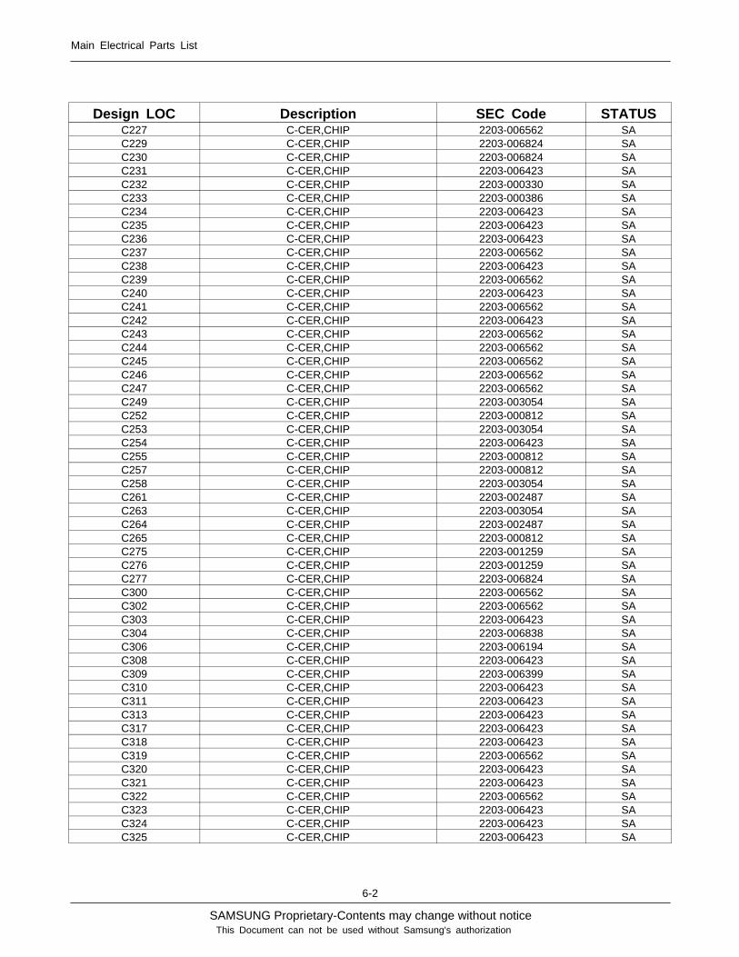
Main Electrical Parts List
6-2
This Document can not be used without Samsung's authorization
Design LOC Description SEC Code STATUSC227 C-CER,CHIP 2203-006562 SAC229 C-CER,CHIP 2203-006824 SAC230 C-CER,CHIP 2203-006824 SAC231 C-CER,CHIP 2203-006423 SAC232 C-CER,CHIP 2203-000330 SAC233 C-CER,CHIP 2203-000386 SAC234 C-CER,CHIP 2203-006423 SAC235 C-CER,CHIP 2203-006423 SAC236 C-CER,CHIP 2203-006423 SAC237 C-CER,CHIP 2203-006562 SAC238 C-CER,CHIP 2203-006423 SAC239 C-CER,CHIP 2203-006562 SAC240 C-CER,CHIP 2203-006423 SAC241 C-CER,CHIP 2203-006562 SAC242 C-CER,CHIP 2203-006423 SAC243 C-CER,CHIP 2203-006562 SAC244 C-CER,CHIP 2203-006562 SAC245 C-CER,CHIP 2203-006562 SAC246 C-CER,CHIP 2203-006562 SAC247 C-CER,CHIP 2203-006562 SAC249 C-CER,CHIP 2203-003054 SAC252 C-CER,CHIP 2203-000812 SAC253 C-CER,CHIP 2203-003054 SAC254 C-CER,CHIP 2203-006423 SAC255 C-CER,CHIP 2203-000812 SAC257 C-CER,CHIP 2203-000812 SAC258 C-CER,CHIP 2203-003054 SAC261 C-CER,CHIP 2203-002487 SAC263 C-CER,CHIP 2203-003054 SAC264 C-CER,CHIP 2203-002487 SAC265 C-CER,CHIP 2203-000812 SAC275 C-CER,CHIP 2203-001259 SAC276 C-CER,CHIP 2203-001259 SAC277 C-CER,CHIP 2203-006824 SAC300 C-CER,CHIP 2203-006562 SAC302 C-CER,CHIP 2203-006562 SAC303 C-CER,CHIP 2203-006423 SAC304 C-CER,CHIP 2203-006838 SAC306 C-CER,CHIP 2203-006194 SAC308 C-CER,CHIP 2203-006423 SAC309 C-CER,CHIP 2203-006399 SAC310 C-CER,CHIP 2203-006423 SAC311 C-CER,CHIP 2203-006423 SAC313 C-CER,CHIP 2203-006423 SAC317 C-CER,CHIP 2203-006423 SAC318 C-CER,CHIP 2203-006423 SAC319 C-CER,CHIP 2203-006562 SAC320 C-CER,CHIP 2203-006423 SAC321 C-CER,CHIP 2203-006423 SAC322 C-CER,CHIP 2203-006562 SAC323 C-CER,CHIP 2203-006423 SAC324 C-CER,CHIP 2203-006423 SAC325 C-CER,CHIP 2203-006423 SA

SAMSUNG Proprietary-Contents may change without notice
Main Electrical Parts List
6-3
This Document can not be used without Samsung's authorization
Design LOC Description SEC Code STATUSC326 C-CER,CHIP 2203-006562 SAC327 C-CER,CHIP 2203-006562 SAC328 C-CER,CHIP 2203-006824 SAC402 C-CER,CHIP 2203-006824 SAC403 C-CER,CHIP 2203-006562 SAC405 C-CER,CHIP 2203-000330 SAC406 C-CER,CHIP 2203-006423 SAC408 C-CER,CHIP 2203-000233 SAC409 C-CER,CHIP 2203-000330 SAC410 C-CER,CHIP 2203-005736 SAC411 C-CER,CHIP 2203-006423 SAC413 C-CER,CHIP 2203-006324 SAC414 C-CER,CHIP 2203-006324 SAC415 C-CER,CHIP 2203-006824 SAC416 C-CER,CHIP 2203-006824 SAC417 C-CER,CHIP 2203-006324 SAC418 C-CER,CHIP 2203-006324 SAC419 C-CER,CHIP 2203-006824 SAC420 C-CER,CHIP 2203-006824 SAC421 C-CER,CHIP 2203-006324 SAC422 C-CER,CHIP 2203-006324 SAC423 C-CER,CHIP 2203-006562 SAC424 C-CER,CHIP 2203-006562 SAC425 C-CER,CHIP 2203-006824 SAC426 C-CER,CHIP 2203-006824 SAC428 C-CER,CHIP 2203-006838 SAC429 C-CER,CHIP 2203-006838 SAC430 C-CER,CHIP 2203-006423 SAC433 C-CER,CHIP 2203-006423 SAC435 C-CER,CHIP 2203-006423 SAC436 C-CER,CHIP 2203-006423 SAC437 C-CER,CHIP 2203-000233 SAC438 C-CER,CHIP 2203-000679 SAC439 C-CER,CHIP 2203-006260 SAC440 C-CER,CHIP 2203-006260 SAC442 C-CER,CHIP 2203-006824 SAC443 C-CER,CHIP 2203-006194 SAC444 C-CER,CHIP 2203-006423 SAC445 C-CER,CHIP 2203-006824 SAC446 C-CER,CHIP 2203-006824 SAC447 C-CER,CHIP 2203-006824 SAC448 C-CER,CHIP 2203-006824 SAC449 C-CER,CHIP 2203-006824 SAC450 C-CER,CHIP 2203-006423 SAC451 C-CER,CHIP 2203-006824 SAC452 C-CER,CHIP 2203-006824 SAC453 C-CER,CHIP 2203-006423 SAC454 C-CER,CHIP 2203-006824 SAC455 C-CER,CHIP 2203-006824 SAC456 C-CER,CHIP 2203-006824 SAC457 C-CER,CHIP 2203-006824 SAC458 C-CER,CHIP 2203-006824 SAC461 C-CER,CHIP 2203-006562 SA
SAMSUNG Proprietary-Contents may change without notice
Main Electrical Parts List
6-4
This Document can not be used without Samsung's authorization
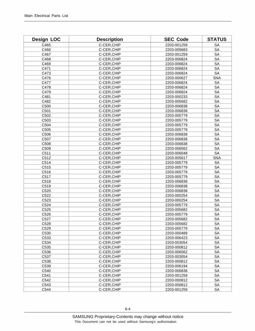
Design LOC Description SEC Code STATUSC465 C-CER,CHIP 2203-001259 SAC466 C-CER,CHIP 2203-005683 SAC467 C-CER,CHIP 2203-001259 SAC468 C-CER,CHIP 2203-006824 SAC469 C-CER,CHIP 2203-006824 SAC471 C-CER,CHIP 2203-006824 SAC473 C-CER,CHIP 2203-006824 SAC476 C-CER,CHIP 2203-000627 SNAC477 C-CER,CHIP 2203-006824 SAC478 C-CER,CHIP 2203-006824 SAC479 C-CER,CHIP 2203-006824 SAC481 C-CER,CHIP 2203-000233 SAC482 C-CER,CHIP 2203-005682 SAC500 C-CER,CHIP 2203-006838 SAC501 C-CER,CHIP 2203-006838 SAC502 C-CER,CHIP 2203-005779 SAC503 C-CER,CHIP 2203-005779 SAC504 C-CER,CHIP 2203-005779 SAC505 C-CER,CHIP 2203-005779 SAC506 C-CER,CHIP 2203-006838 SAC507 C-CER,CHIP 2203-006838 SAC508 C-CER,CHIP 2203-006838 SAC509 C-CER,CHIP 2203-006562 SAC511 C-CER,CHIP 2203-006048 SAC512 C-CER,CHIP 2203-005617 SNAC514 C-CER,CHIP 2203-005779 SAC515 C-CER,CHIP 2203-005779 SAC516 C-CER,CHIP 2203-005779 SAC517 C-CER,CHIP 2203-005779 SAC518 C-CER,CHIP 2203-006838 SAC519 C-CER,CHIP 2203-006838 SAC520 C-CER,CHIP 2203-006838 SAC522 C-CER,CHIP 2203-000254 SAC523 C-CER,CHIP 2203-000254 SAC524 C-CER,CHIP 2203-005779 SAC525 C-CER,CHIP 2203-005682 SAC526 C-CER,CHIP 2203-005779 SAC527 C-CER,CHIP 2203-005682 SAC528 C-CER,CHIP 2203-005682 SAC529 C-CER,CHIP 2203-005779 SAC530 C-CER,CHIP 2203-000489 SAC533 C-CER,CHIP 2203-006423 SAC534 C-CER,CHIP 2203-003054 SAC535 C-CER,CHIP 2203-000812 SAC536 C-CER,CHIP 2203-006562 SAC537 C-CER,CHIP 2203-003054 SAC538 C-CER,CHIP 2203-000812 SAC539 C-CER,CHIP 2203-006194 SAC540 C-CER,CHIP 2203-006838 SAC541 C-CER,CHIP 2203-001259 SAC542 C-CER,CHIP 2203-000812 SAC543 C-CER,CHIP 2203-000812 SAC544 C-CER,CHIP 2203-001259 SA
SAMSUNG Proprietary-Contents may change without notice
Main Electrical Parts List
6-5
This Document can not be used without Samsung's authorization
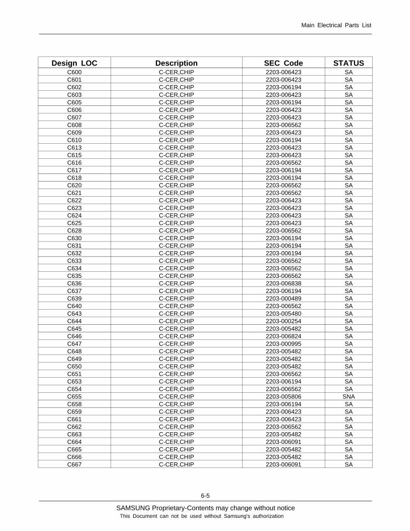
Design LOC Description SEC Code STATUSC600 C-CER,CHIP 2203-006423 SAC601 C-CER,CHIP 2203-006423 SAC602 C-CER,CHIP 2203-006194 SAC603 C-CER,CHIP 2203-006423 SAC605 C-CER,CHIP 2203-006194 SAC606 C-CER,CHIP 2203-006423 SAC607 C-CER,CHIP 2203-006423 SAC608 C-CER,CHIP 2203-006562 SAC609 C-CER,CHIP 2203-006423 SAC610 C-CER,CHIP 2203-006194 SAC613 C-CER,CHIP 2203-006423 SAC615 C-CER,CHIP 2203-006423 SAC616 C-CER,CHIP 2203-006562 SAC617 C-CER,CHIP 2203-006194 SAC618 C-CER,CHIP 2203-006194 SAC620 C-CER,CHIP 2203-006562 SAC621 C-CER,CHIP 2203-006562 SAC622 C-CER,CHIP 2203-006423 SAC623 C-CER,CHIP 2203-006423 SAC624 C-CER,CHIP 2203-006423 SAC625 C-CER,CHIP 2203-006423 SAC628 C-CER,CHIP 2203-006562 SAC630 C-CER,CHIP 2203-006194 SAC631 C-CER,CHIP 2203-006194 SAC632 C-CER,CHIP 2203-006194 SAC633 C-CER,CHIP 2203-006562 SAC634 C-CER,CHIP 2203-006562 SAC635 C-CER,CHIP 2203-006562 SAC636 C-CER,CHIP 2203-006838 SAC637 C-CER,CHIP 2203-006194 SAC639 C-CER,CHIP 2203-000489 SAC640 C-CER,CHIP 2203-006562 SAC643 C-CER,CHIP 2203-005480 SAC644 C-CER,CHIP 2203-000254 SAC645 C-CER,CHIP 2203-005482 SAC646 C-CER,CHIP 2203-006824 SAC647 C-CER,CHIP 2203-000995 SAC648 C-CER,CHIP 2203-005482 SAC649 C-CER,CHIP 2203-005482 SAC650 C-CER,CHIP 2203-005482 SAC651 C-CER,CHIP 2203-006562 SAC653 C-CER,CHIP 2203-006194 SAC654 C-CER,CHIP 2203-006562 SAC655 C-CER,CHIP 2203-005806 SNAC658 C-CER,CHIP 2203-006194 SAC659 C-CER,CHIP 2203-006423 SAC661 C-CER,CHIP 2203-006423 SAC662 C-CER,CHIP 2203-006562 SAC663 C-CER,CHIP 2203-005482 SAC664 C-CER,CHIP 2203-006091 SAC665 C-CER,CHIP 2203-005482 SAC666 C-CER,CHIP 2203-005482 SAC667 C-CER,CHIP 2203-006091 SA
SAMSUNG Proprietary-Contents may change without notice
Main Electrical Parts List
6-6
This Document can not be used without Samsung's authorization
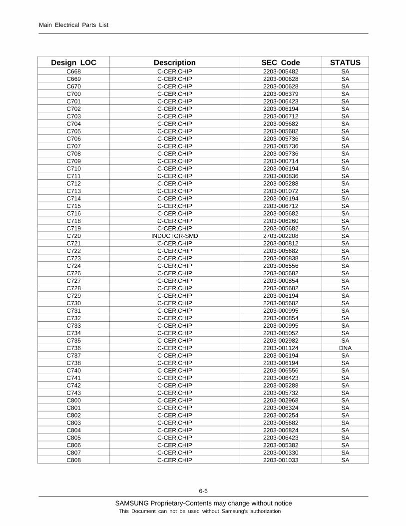
Design LOC Description SEC Code STATUSC668 C-CER,CHIP 2203-005482 SAC669 C-CER,CHIP 2203-000628 SAC670 C-CER,CHIP 2203-000628 SAC700 C-CER,CHIP 2203-006379 SAC701 C-CER,CHIP 2203-006423 SAC702 C-CER,CHIP 2203-006194 SAC703 C-CER,CHIP 2203-006712 SAC704 C-CER,CHIP 2203-005682 SAC705 C-CER,CHIP 2203-005682 SAC706 C-CER,CHIP 2203-005736 SAC707 C-CER,CHIP 2203-005736 SAC708 C-CER,CHIP 2203-005736 SAC709 C-CER,CHIP 2203-000714 SAC710 C-CER,CHIP 2203-006194 SAC711 C-CER,CHIP 2203-000836 SAC712 C-CER,CHIP 2203-005288 SAC713 C-CER,CHIP 2203-001072 SAC714 C-CER,CHIP 2203-006194 SAC715 C-CER,CHIP 2203-006712 SAC716 C-CER,CHIP 2203-005682 SAC718 C-CER,CHIP 2203-006260 SAC719 C-CER,CHIP 2203-005682 SAC720 INDUCTOR-SMD 2703-002208 SAC721 C-CER,CHIP 2203-000812 SAC722 C-CER,CHIP 2203-005682 SAC723 C-CER,CHIP 2203-006838 SAC724 C-CER,CHIP 2203-006556 SAC726 C-CER,CHIP 2203-005682 SAC727 C-CER,CHIP 2203-000854 SAC728 C-CER,CHIP 2203-005682 SAC729 C-CER,CHIP 2203-006194 SAC730 C-CER,CHIP 2203-005682 SAC731 C-CER,CHIP 2203-000995 SAC732 C-CER,CHIP 2203-000854 SAC733 C-CER,CHIP 2203-000995 SAC734 C-CER,CHIP 2203-005052 SAC735 C-CER,CHIP 2203-002982 SAC736 C-CER,CHIP 2203-001124 DNAC737 C-CER,CHIP 2203-006194 SAC738 C-CER,CHIP 2203-006194 SAC740 C-CER,CHIP 2203-006556 SAC741 C-CER,CHIP 2203-006423 SAC742 C-CER,CHIP 2203-005288 SAC743 C-CER,CHIP 2203-005732 SAC800 C-CER,CHIP 2203-002968 SAC801 C-CER,CHIP 2203-006324 SAC802 C-CER,CHIP 2203-000254 SAC803 C-CER,CHIP 2203-005682 SAC804 C-CER,CHIP 2203-006824 SAC805 C-CER,CHIP 2203-006423 SAC806 C-CER,CHIP 2203-005382 SAC807 C-CER,CHIP 2203-000330 SAC808 C-CER,CHIP 2203-001033 SA
SAMSUNG Proprietary-Contents may change without notice
Main Electrical Parts List
6-7
This Document can not be used without Samsung's authorization
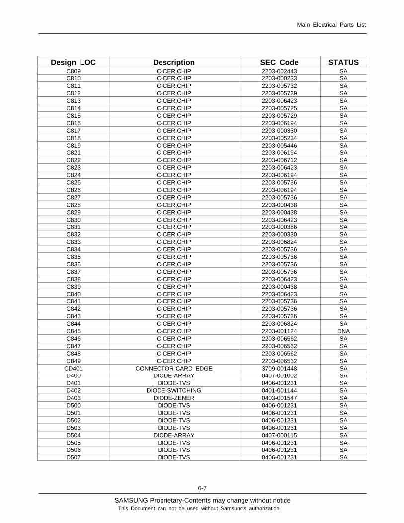
Design LOC Description SEC Code STATUSC809 C-CER,CHIP 2203-002443 SAC810 C-CER,CHIP 2203-000233 SAC811 C-CER,CHIP 2203-005732 SAC812 C-CER,CHIP 2203-005729 SAC813 C-CER,CHIP 2203-006423 SAC814 C-CER,CHIP 2203-005725 SAC815 C-CER,CHIP 2203-005729 SAC816 C-CER,CHIP 2203-006194 SAC817 C-CER,CHIP 2203-000330 SAC818 C-CER,CHIP 2203-005234 SAC819 C-CER,CHIP 2203-005446 SAC821 C-CER,CHIP 2203-006194 SAC822 C-CER,CHIP 2203-006712 SAC823 C-CER,CHIP 2203-006423 SAC824 C-CER,CHIP 2203-006194 SAC825 C-CER,CHIP 2203-005736 SAC826 C-CER,CHIP 2203-006194 SAC827 C-CER,CHIP 2203-005736 SAC828 C-CER,CHIP 2203-000438 SAC829 C-CER,CHIP 2203-000438 SAC830 C-CER,CHIP 2203-006423 SAC831 C-CER,CHIP 2203-000386 SAC832 C-CER,CHIP 2203-000330 SAC833 C-CER,CHIP 2203-006824 SAC834 C-CER,CHIP 2203-005736 SAC835 C-CER,CHIP 2203-005736 SAC836 C-CER,CHIP 2203-005736 SAC837 C-CER,CHIP 2203-005736 SAC838 C-CER,CHIP 2203-006423 SAC839 C-CER,CHIP 2203-000438 SAC840 C-CER,CHIP 2203-006423 SAC841 C-CER,CHIP 2203-005736 SAC842 C-CER,CHIP 2203-005736 SAC843 C-CER,CHIP 2203-005736 SAC844 C-CER,CHIP 2203-006824 SAC845 C-CER,CHIP 2203-001124 DNAC846 C-CER,CHIP 2203-006562 SAC847 C-CER,CHIP 2203-006562 SAC848 C-CER,CHIP 2203-006562 SAC849 C-CER,CHIP 2203-006562 SA
CD401 CONNECTOR-CARD EDGE 3709-001448 SAD400 DIODE-ARRAY 0407-001002 SAD401 DIODE-TVS 0406-001231 SAD402 DIODE-SWITCHING 0401-001144 SAD403 DIODE-ZENER 0403-001547 SAD500 DIODE-TVS 0406-001231 SAD501 DIODE-TVS 0406-001231 SAD502 DIODE-TVS 0406-001231 SAD503 DIODE-TVS 0406-001231 SAD504 DIODE-ARRAY 0407-000115 SAD505 DIODE-TVS 0406-001231 SAD506 DIODE-TVS 0406-001231 SAD507 DIODE-TVS 0406-001231 SA
SAMSUNG Proprietary-Contents may change without notice
Main Electrical Parts List
6-8
This Document can not be used without Samsung's authorization
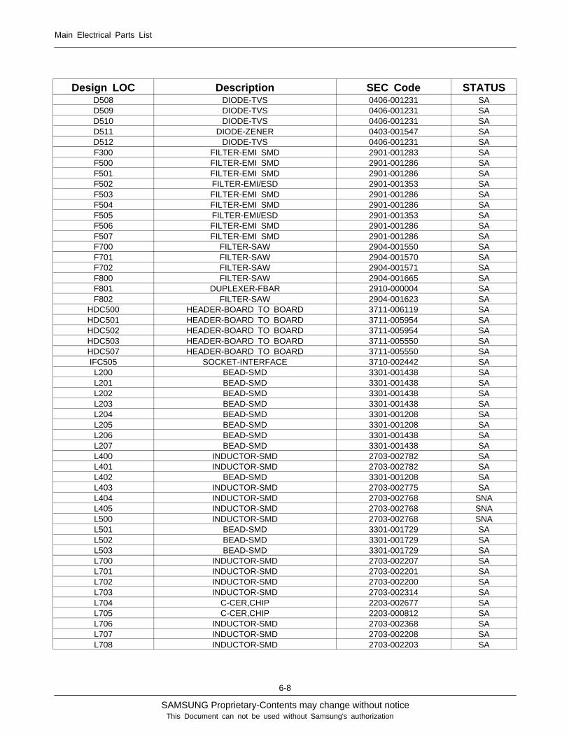
Design LOC Description SEC Code STATUSD508 DIODE-TVS 0406-001231 SAD509 DIODE-TVS 0406-001231 SAD510 DIODE-TVS 0406-001231 SAD511 DIODE-ZENER 0403-001547 SAD512 DIODE-TVS 0406-001231 SAF300 FILTER-EMI SMD 2901-001283 SAF500 FILTER-EMI SMD 2901-001286 SAF501 FILTER-EMI SMD 2901-001286 SAF502 FILTER-EMI/ESD 2901-001353 SAF503 FILTER-EMI SMD 2901-001286 SAF504 FILTER-EMI SMD 2901-001286 SAF505 FILTER-EMI/ESD 2901-001353 SAF506 FILTER-EMI SMD 2901-001286 SAF507 FILTER-EMI SMD 2901-001286 SAF700 FILTER-SAW 2904-001550 SAF701 FILTER-SAW 2904-001570 SAF702 FILTER-SAW 2904-001571 SAF800 FILTER-SAW 2904-001665 SAF801 DUPLEXER-FBAR 2910-000004 SAF802 FILTER-SAW 2904-001623 SA
HDC500 HEADER-BOARD TO BOARD 3711-006119 SAHDC501 HEADER-BOARD TO BOARD 3711-005954 SAHDC502 HEADER-BOARD TO BOARD 3711-005954 SAHDC503 HEADER-BOARD TO BOARD 3711-005550 SAHDC507 HEADER-BOARD TO BOARD 3711-005550 SAIFC505 SOCKET-INTERFACE 3710-002442 SAL200 BEAD-SMD 3301-001438 SAL201 BEAD-SMD 3301-001438 SAL202 BEAD-SMD 3301-001438 SAL203 BEAD-SMD 3301-001438 SAL204 BEAD-SMD 3301-001208 SAL205 BEAD-SMD 3301-001208 SAL206 BEAD-SMD 3301-001438 SAL207 BEAD-SMD 3301-001438 SAL400 INDUCTOR-SMD 2703-002782 SAL401 INDUCTOR-SMD 2703-002782 SAL402 BEAD-SMD 3301-001208 SAL403 INDUCTOR-SMD 2703-002775 SAL404 INDUCTOR-SMD 2703-002768 SNAL405 INDUCTOR-SMD 2703-002768 SNAL500 INDUCTOR-SMD 2703-002768 SNAL501 BEAD-SMD 3301-001729 SAL502 BEAD-SMD 3301-001729 SAL503 BEAD-SMD 3301-001729 SAL700 INDUCTOR-SMD 2703-002207 SAL701 INDUCTOR-SMD 2703-002201 SAL702 INDUCTOR-SMD 2703-002200 SAL703 INDUCTOR-SMD 2703-002314 SAL704 C-CER,CHIP 2203-002677 SAL705 C-CER,CHIP 2203-000812 SAL706 INDUCTOR-SMD 2703-002368 SAL707 INDUCTOR-SMD 2703-002208 SAL708 INDUCTOR-SMD 2703-002203 SA
SAMSUNG Proprietary-Contents may change without notice
Main Electrical Parts List
6-9
This Document can not be used without Samsung's authorization
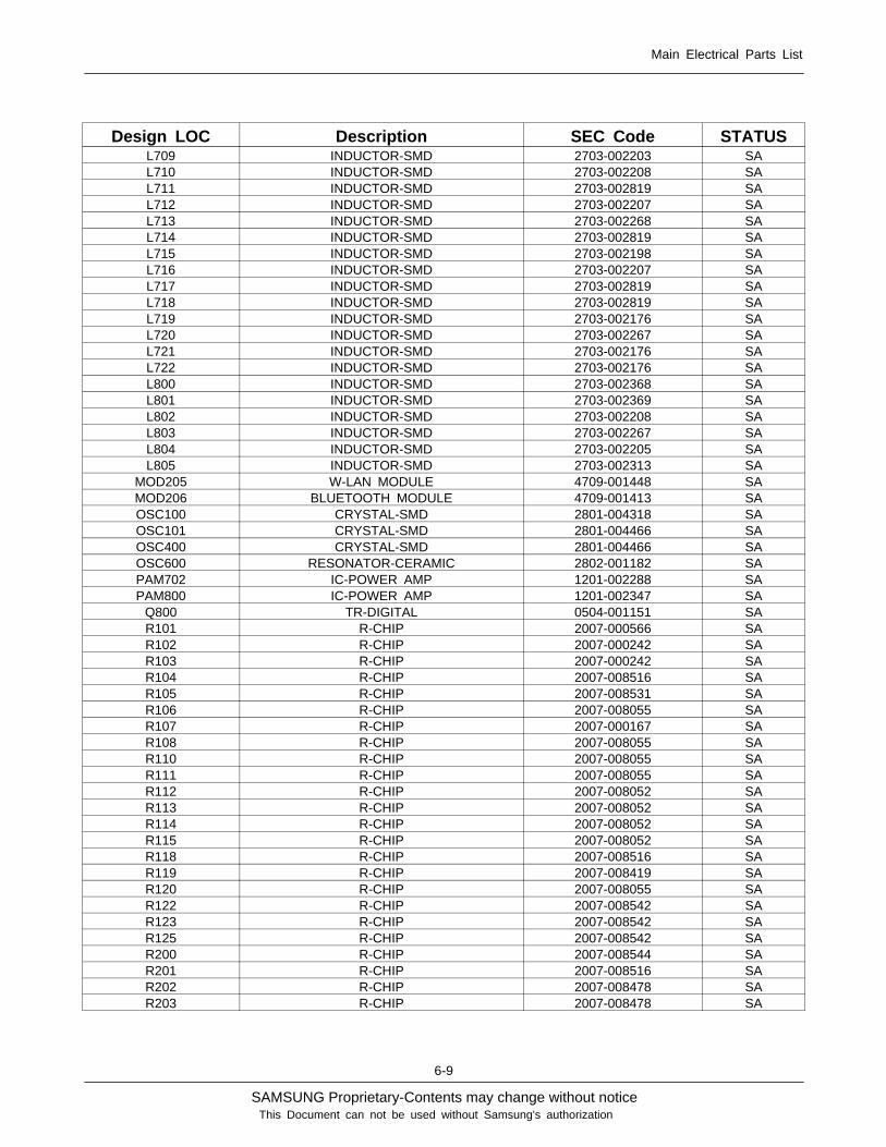
Design LOC Description SEC Code STATUSL709 INDUCTOR-SMD 2703-002203 SAL710 INDUCTOR-SMD 2703-002208 SAL711 INDUCTOR-SMD 2703-002819 SAL712 INDUCTOR-SMD 2703-002207 SAL713 INDUCTOR-SMD 2703-002268 SAL714 INDUCTOR-SMD 2703-002819 SAL715 INDUCTOR-SMD 2703-002198 SAL716 INDUCTOR-SMD 2703-002207 SAL717 INDUCTOR-SMD 2703-002819 SAL718 INDUCTOR-SMD 2703-002819 SAL719 INDUCTOR-SMD 2703-002176 SAL720 INDUCTOR-SMD 2703-002267 SAL721 INDUCTOR-SMD 2703-002176 SAL722 INDUCTOR-SMD 2703-002176 SAL800 INDUCTOR-SMD 2703-002368 SAL801 INDUCTOR-SMD 2703-002369 SAL802 INDUCTOR-SMD 2703-002208 SAL803 INDUCTOR-SMD 2703-002267 SAL804 INDUCTOR-SMD 2703-002205 SAL805 INDUCTOR-SMD 2703-002313 SA
MOD205 W-LAN MODULE 4709-001448 SAMOD206 BLUETOOTH MODULE 4709-001413 SAOSC100 CRYSTAL-SMD 2801-004318 SAOSC101 CRYSTAL-SMD 2801-004466 SAOSC400 CRYSTAL-SMD 2801-004466 SAOSC600 RESONATOR-CERAMIC 2802-001182 SAPAM702 IC-POWER AMP 1201-002288 SAPAM800 IC-POWER AMP 1201-002347 SA
Q800 TR-DIGITAL 0504-001151 SAR101 R-CHIP 2007-000566 SAR102 R-CHIP 2007-000242 SAR103 R-CHIP 2007-000242 SAR104 R-CHIP 2007-008516 SAR105 R-CHIP 2007-008531 SAR106 R-CHIP 2007-008055 SAR107 R-CHIP 2007-000167 SAR108 R-CHIP 2007-008055 SAR110 R-CHIP 2007-008055 SAR111 R-CHIP 2007-008055 SAR112 R-CHIP 2007-008052 SAR113 R-CHIP 2007-008052 SAR114 R-CHIP 2007-008052 SAR115 R-CHIP 2007-008052 SAR118 R-CHIP 2007-008516 SAR119 R-CHIP 2007-008419 SAR120 R-CHIP 2007-008055 SAR122 R-CHIP 2007-008542 SAR123 R-CHIP 2007-008542 SAR125 R-CHIP 2007-008542 SAR200 R-CHIP 2007-008544 SAR201 R-CHIP 2007-008516 SAR202 R-CHIP 2007-008478 SAR203 R-CHIP 2007-008478 SA
SAMSUNG Proprietary-Contents may change without notice
Main Electrical Parts List
6-10
This Document can not be used without Samsung's authorization
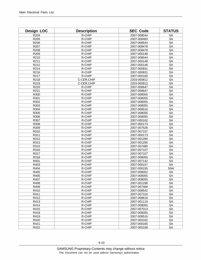
Design LOC Description SEC Code STATUSR204 R-CHIP 2007-008544 SAR205 R-CHIP 2007-008483 SAR206 R-CHIP 2007-008544 SAR207 R-CHIP 2007-008478 SAR208 R-CHIP 2007-008478 SAR209 R-CHIP 2007-000148 SAR210 R-CHIP 2007-008544 SAR211 R-CHIP 2007-000148 SAR212 R-CHIP 2007-000148 SAR214 R-CHIP 2007-000831 SAR216 R-CHIP 2007-000831 SAR217 R-CHIP 2007-000165 SAR218 C-CER,CHIP 2203-000812 SAR219 C-CER,CHIP 2203-000812 SAR220 R-CHIP 2007-008647 SAR221 R-CHIP 2007-008647 SAR300 R-CHIP 2007-008055 SAR301 R-CHIP 2007-008055 SAR302 R-CHIP 2007-008055 SAR303 R-CHIP 2007-008055 SAR304 R-CHIP 2007-008516 SAR305 R-CHIP 2007-008055 SAR306 R-CHIP 2007-008055 SAR307 R-CHIP 2007-000162 SAR308 R-CHIP 2007-000173 SAR309 R-CHIP 2007-007528 SAR310 R-CHIP 2007-007107 SAR311 R-CHIP 2007-000173 SAR312 R-CHIP 2007-001290 SAR313 R-CHIP 2007-001290 SAR315 R-CHIP 2007-007489 SAR316 R-CHIP 2007-007107 SAR317 R-CHIP 2007-007107 SAR318 R-CHIP 2007-008055 SAR401 R-CHIP 2007-007142 SAR403 R-CHIP 2007-000157 SAR404 R-CHIP 2007-009155 SNAR405 R-CHIP 2007-008052 SAR406 R-CHIP 2007-008055 SAR407 R-CHIP 2007-008055 SAR408 R-CHIP 2007-001298 SAR409 R-CHIP 2007-007468 SAR410 R-CHIP 2007-008542 SAR411 R-CHIP 2007-007316 SAR412 R-CHIP 2007-008616 SAR413 R-CHIP 2007-001119 SAR414 R-CHIP 2007-008055 SAR415 R-CHIP 2007-007013 SAR418 R-CHIP 2007-008055 SAR419 R-CHIP 2007-008516 SAR420 R-CHIP 2007-000162 SAR421 R-CHIP 2007-000165 SAR422 R-CHIP 2007-000168 SA
SAMSUNG Proprietary-Contents may change without notice
Main Electrical Parts List
6-11
This Document can not be used without Samsung's authorization
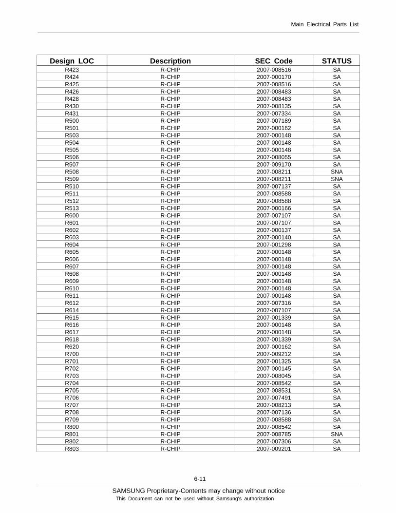
Design LOC Description SEC Code STATUSR423 R-CHIP 2007-008516 SAR424 R-CHIP 2007-000170 SAR425 R-CHIP 2007-008516 SAR426 R-CHIP 2007-008483 SAR428 R-CHIP 2007-008483 SAR430 R-CHIP 2007-008135 SAR431 R-CHIP 2007-007334 SAR500 R-CHIP 2007-007189 SAR501 R-CHIP 2007-000162 SAR503 R-CHIP 2007-000148 SAR504 R-CHIP 2007-000148 SAR505 R-CHIP 2007-000148 SAR506 R-CHIP 2007-008055 SAR507 R-CHIP 2007-009170 SAR508 R-CHIP 2007-008211 SNAR509 R-CHIP 2007-008211 SNAR510 R-CHIP 2007-007137 SAR511 R-CHIP 2007-008588 SAR512 R-CHIP 2007-008588 SAR513 R-CHIP 2007-000166 SAR600 R-CHIP 2007-007107 SAR601 R-CHIP 2007-007107 SAR602 R-CHIP 2007-000137 SAR603 R-CHIP 2007-000140 SAR604 R-CHIP 2007-001298 SAR605 R-CHIP 2007-000148 SAR606 R-CHIP 2007-000148 SAR607 R-CHIP 2007-000148 SAR608 R-CHIP 2007-000148 SAR609 R-CHIP 2007-000148 SAR610 R-CHIP 2007-000148 SAR611 R-CHIP 2007-000148 SAR612 R-CHIP 2007-007316 SAR614 R-CHIP 2007-007107 SAR615 R-CHIP 2007-001339 SAR616 R-CHIP 2007-000148 SAR617 R-CHIP 2007-000148 SAR618 R-CHIP 2007-001339 SAR620 R-CHIP 2007-000162 SAR700 R-CHIP 2007-009212 SAR701 R-CHIP 2007-001325 SAR702 R-CHIP 2007-000145 SAR703 R-CHIP 2007-008045 SAR704 R-CHIP 2007-008542 SAR705 R-CHIP 2007-008531 SAR706 R-CHIP 2007-007491 SAR707 R-CHIP 2007-008213 SAR708 R-CHIP 2007-007136 SAR709 R-CHIP 2007-008588 SAR800 R-CHIP 2007-008542 SAR801 R-CHIP 2007-008785 SNAR802 R-CHIP 2007-007306 SAR803 R-CHIP 2007-009201 SA
SAMSUNG Proprietary-Contents may change without notice
Main Electrical Parts List
6-12
This Document can not be used without Samsung's authorization
Design LOC Description SEC Code STATUSR804 R-CHIP 2007-001292 SAR805 R-CHIP 2007-008542 SAR806 R-CHIP 2007-008581 SNAR807 R-CHIP 2007-008581 SNAR808 R-CHIP 2007-008045 SAR809 R-CHIP 2007-008579 SAR810 R-CHIP 2007-008579 SAR811 R-CHIP 2007-008045 SAR812 R-CHIP 2007-008806 SAR813 R-CHIP 2007-008045 SAR814 R-CHIP 2007-008045 SAR815 R-CHIP 2007-007491 SAR816 R-CHIP 2007-007318 SAR817 R-CHIP 2007-008531 SAR818 R-CHIP 2007-001217 SAR819 R-CHIP 2007-008531 SAR820 R-CHIP 2007-000171 SAR822 R-CHIP 2007-009155 SNAR823 R-CHIP 2007-009170 SAR824 R-CHIP 2007-008055 SA
RFS700 CONNECTOR-COAXIAL 3705-001358 SASIM400 CONNECTOR-CARD EDGE 3709-001474 SASLC504 CONNECTOR-FPC/FFC/PIC 3708-002162 SASOC508 SOCKET-BOARD TO BOARD 3710-002081 SATA201 C-TA,CHIP 2404-001377 SATA209 C-TA,CHIP 2404-001352 SATA210 C-TA,CHIP 2404-001281 SATA211 C-TA,CHIP 2404-001281 SATA221 C-TA,CHIP 2404-001377 SATA228 C-TA,CHIP 2404-001352 SATA256 C-TA,CHIP 2404-001474 SATA401 C-TA,CHIP 2404-001474 SATA459 C-TA,CHIP 2404-001474 SATA460 C-TA,CHIP 2404-001474 SATA462 C-TA,CHIP 2404-001281 SATA474 C-TA,CHIP 2404-001474 SATA475 C-TA,CHIP 2404-001396 SATA480 C-TA,CHIP 2404-001281 SATA521 C-TA,CHIP 2404-001474 SATA532 C-TA,CHIP 2404-001381 SATA739 C-TA,CHIP 2404-001474 SA
TCX801 OSCILLATOR-VCTCXO 2809-001277 SATH301 THERMISTOR-NTC 1404-001221 SATH701 THERMISTOR-NTC 1404-001221 SATR401 FET-SILICON 0505-001165 SATR402 TR-DIGITAL 0504-001171 SATR403 TR-DIGITAL 0504-001171 SATR404 TR-DIGITAL 0504-001171 SAU100 IC-EXPANDER 1205-003075 SAU201 IC-ANALOG SWITCH 1001-001354 SAU202 IC-ANALOG SWITCH 1001-001354 SAU203 IC-AUDIO AMP 1201-002304 SAU204 IC-ANALOG SWITCH 1001-001394 SA
SAMSUNG Proprietary-Contents may change without notice
Main Electrical Parts List
6-13
This Document can not be used without Samsung's authorization
Design LOC Description SEC Code STATUSU302 IC-CMOS LOGIC 0801-003016 SAU303 IC-CMOS LOGIC 0801-003022 SAU304 IC-CMOS LOGIC 0801-003052 SAU305 IC-CMOS LOGIC 0801-002529 SAU306 IC-CMOS LOGIC 0801-002321 SAU307 IC-TRANSCEIVER 1205-002272 SAU308 IC-D/A CONVERTER 1002-001488 SAU309 IC-ANALOG SWITCH 1001-001221 SAU310 IC-SWITCH 1205-002784 SAU400 IC-POWER SUPERVISOR 1203-004102 SAU401 IC-BATTERY 1203-003823 SAU402 IC-LEVEL DRIVER 1003-001984 SAU403 IC-DC/DC CONVERTER 1203-004416 SAU404 IC-RESET 1203-004142 SAU405 IC-VOL. DETECTOR 1203-003924 SAU406 IC-POSI.FIXED REG. 1203-003787 SAU407 IC-POSI.FIXED REG. 1203-004458 SAU408 IC-POSI.FIXED REG. 1203-004419 SAU409 IC-MULTI REG. 1203-004340 SAU410 IC-POSI.FIXED REG. 1203-003688 SAU411 IC-ANALOG SWITCH 1001-001359 SAU413 IC-MULTI REG. 1203-004120 SAU414 IC-MULTI REG. 1203-004447 SAU415 IC-DC/DC CONVERTER 1203-003538 SAU416 IC-VOL. DETECTOR 1203-002716 SAU417 IC-DC/DC CONVERTER 1203-003919 SAU418 IC-MULTI REG. 1203-004120 SAU500 IC-DC/DC CONVERTER 1203-004172 SAU501 IC-CMOS LOGIC 0801-003136 SAU602 IC-CMOS LOGIC 0801-003016 SAU700 IC-TRANSCEIVER 1205-002645 SAU701 IC-SWITCH 1205-002724 SAU801 IC-DETECTOR 1209-001577 SAU802 IC-RECEIVER 1205-002781 SAU804 IC-SWITCH 1205-002874 SNAU805 R-CHIP 2007-000162 SA
UCD200 IC-CODEC 1205-002719 SAUCP101 IC-DSP 0904-002074 SAUCP600 IC-MODEM 1205-002790 SAUME300 IC-SRAM 1106-001511 SAUME301 IC-MCP 1108-000043 SAUME601 IC-MCP 1108-000088 SAVCO800 OSCILLATOR-VCO 2806-001377 SAZD500 DIODE-TVS 0406-001210 SAZD501 DIODE-TVS 0406-001210 SAZD502 DIODE-TVS 0406-001210 SAZD503 DIODE-TVS 0406-001210 SAZD504 DIODE-TVS 0406-001190 SAZD505 DIODE-TVS 0406-001167 SAZD506 DIODE-TVS 0406-001167 SAZD507 DIODE-TVS 0406-001167 SAZD508 DIODE-TVS 0406-001167 SAZD509 DIODE-ZENER 0403-001446 SA
SAMSUNG Proprietary-Contents may change without notice
Main Electrical Parts List
6-14
This Document can not be used without Samsung's authorization
Design LOC Description SEC Code STATUSZD510 DIODE-ZENER 0403-001427 SA
SAMSUNG Proprietary-Contents may change without noticeThis Document can not be used without Samsung's authorization
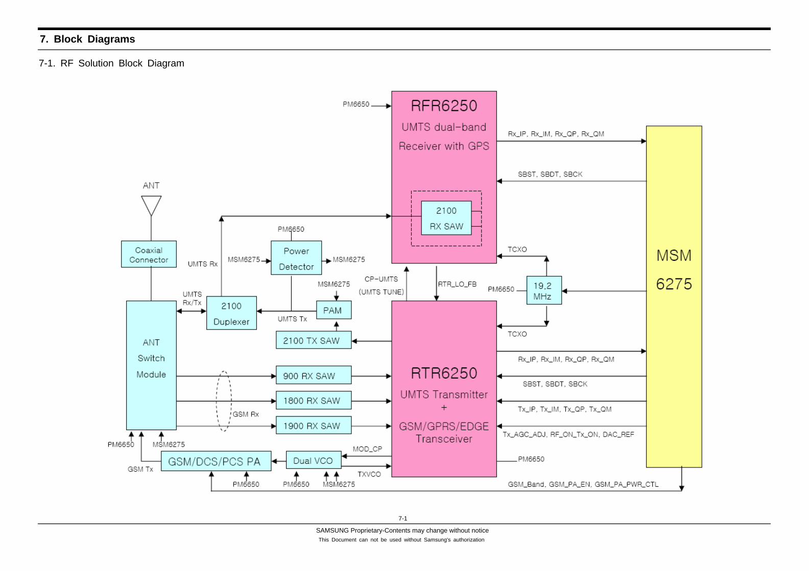
7. Block Diagrams
7-1
7-1. RF Solution Block Diagram
SAMSUNG Proprietary-Contents may change without notice
Block Diagrams
7-2
This Document can not be used without Samsung's authorization
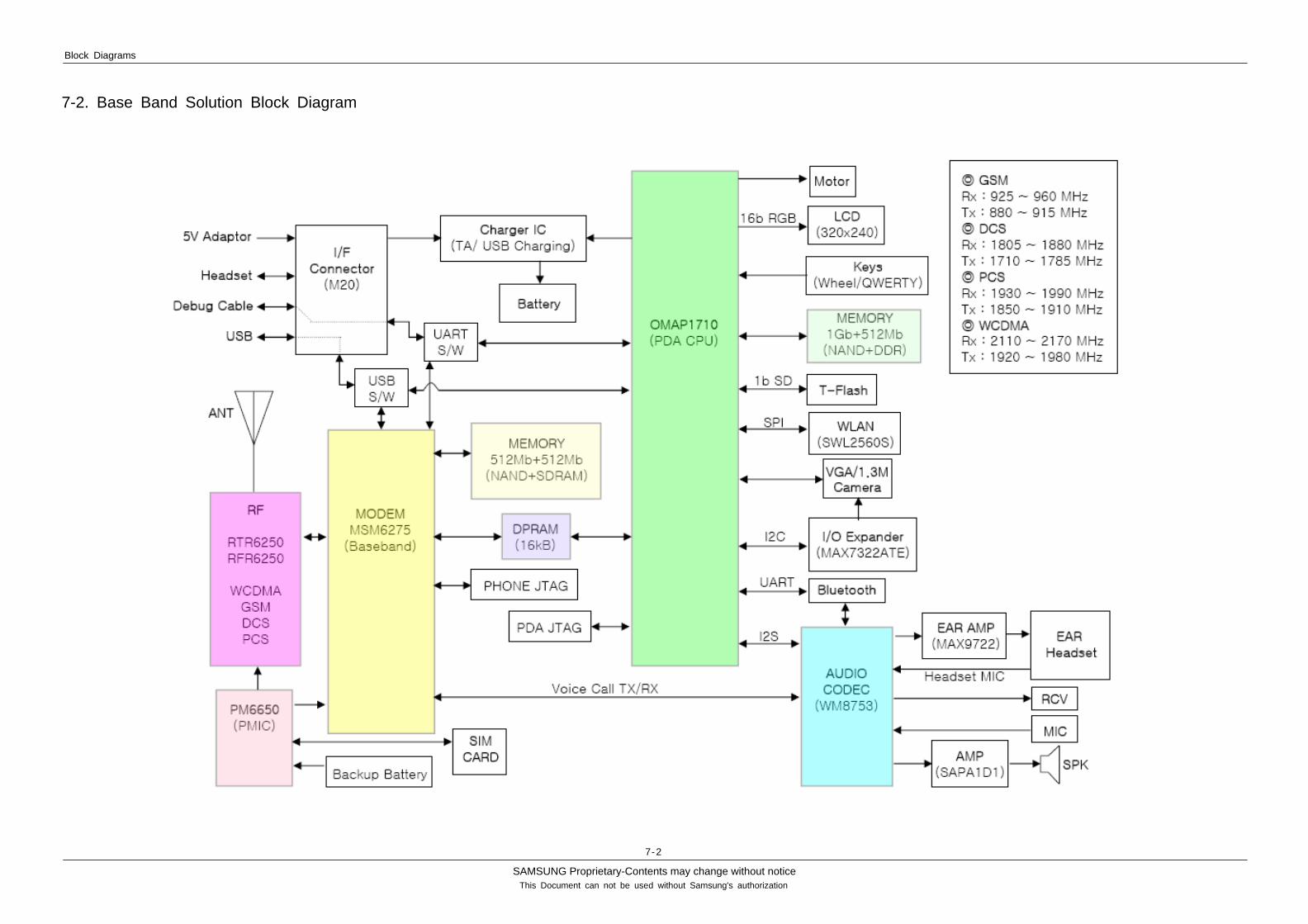
7-2. Base Band Solution Block Diagram
SAMSUNG Proprietary-Contents may change without notice
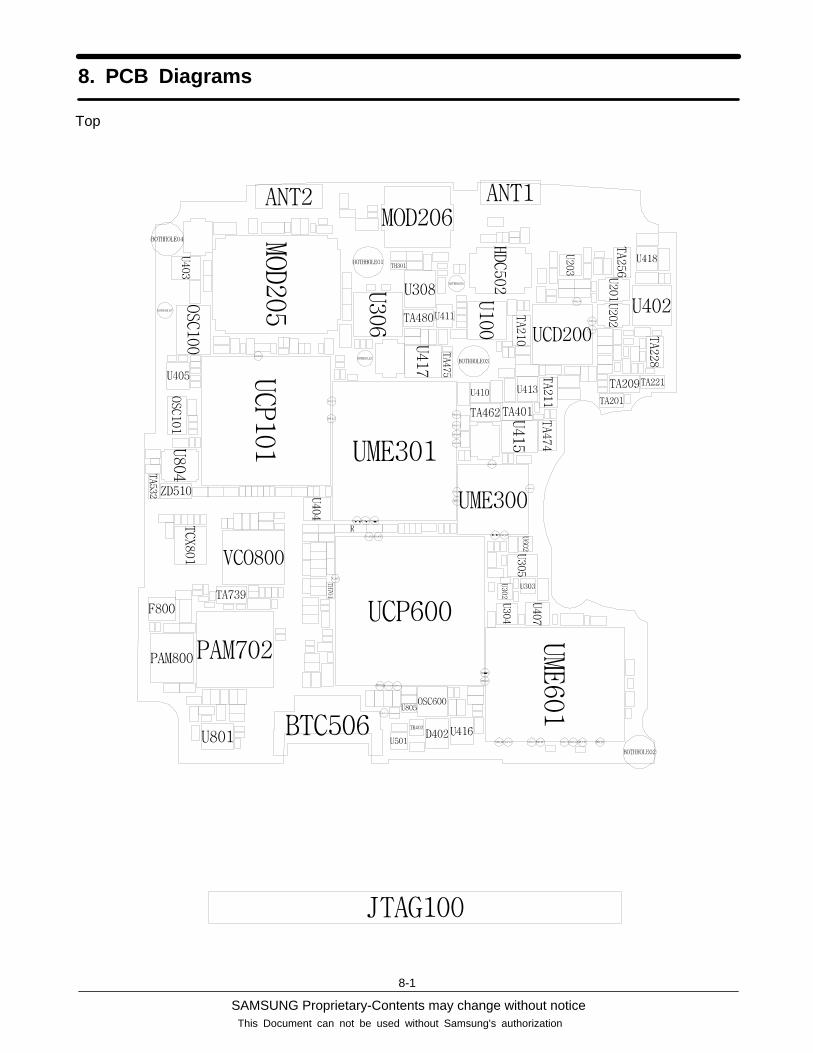
8. PCB Diagrams
8-1
This Document can not be used without Samsung's authorization
Top
SAMSUNG Proprietary-Contents may change without notice
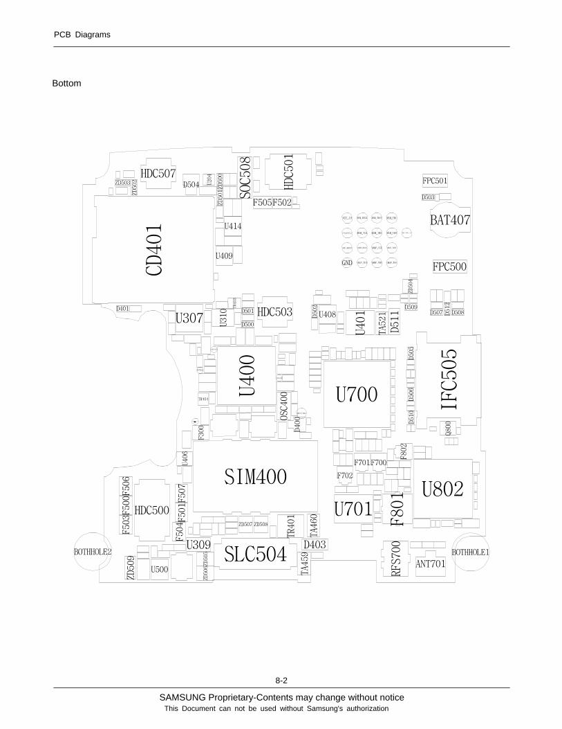
PCB Diagrams
8-2
This Document can not be used without Samsung's authorization
Bottom
SAMSUNG Proprietary-Contents may change without notice
9. Flow Chart of TroubleShooting
9-1
This Document can not be used without Samsung's authorization
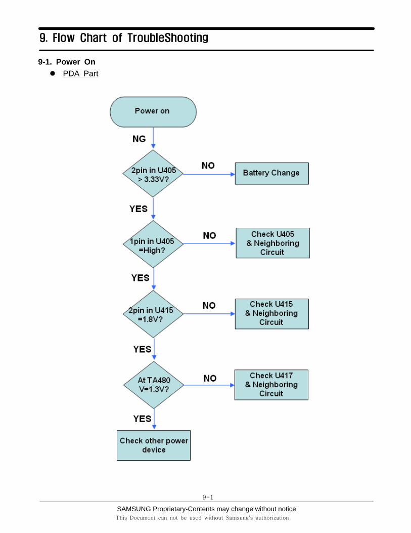
9-1. Power OnPDA Part
SAMSUNG Proprietary-Contents may change without notice
Flow Chart of Troubleshooting
9-2
This Document can not be used without Samsung's authorization
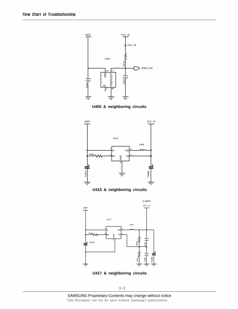
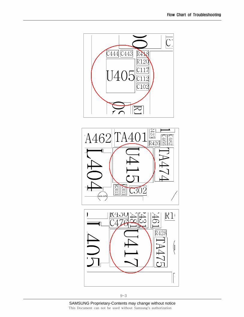
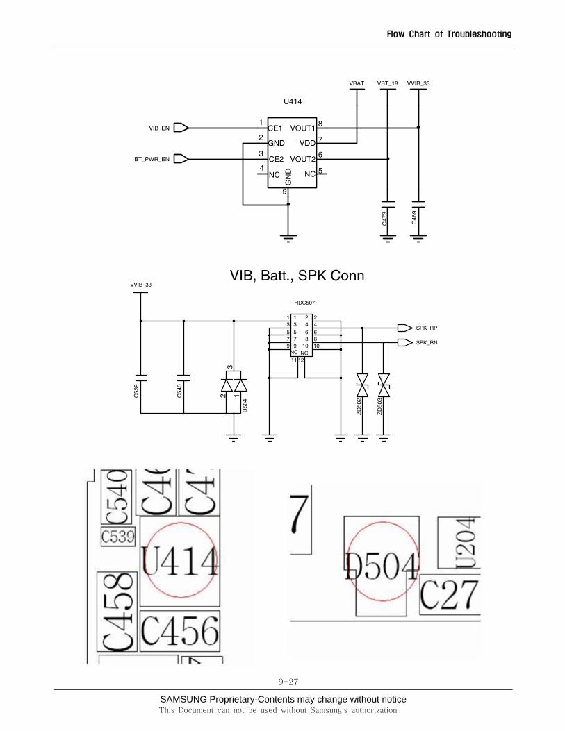
U405 & neighboring circuits
U415 & neighboring circuits
U417 & neighboring circuits
SAMSUNG Proprietary-Contents may change without notice
Flow Chart of Troubleshooting
9-3
This Document can not be used without Samsung's authorization
SAMSUNG Proprietary-Contents may change without notice
Flow Chart of Troubleshooting
9-4
This Document can not be used without Samsung's authorization
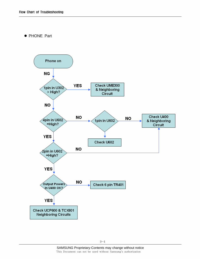
PHONE Part
SAMSUNG Proprietary-Contents may change without notice
Flow Chart of Troubleshooting
9-5
This Document can not be used without Samsung's authorization
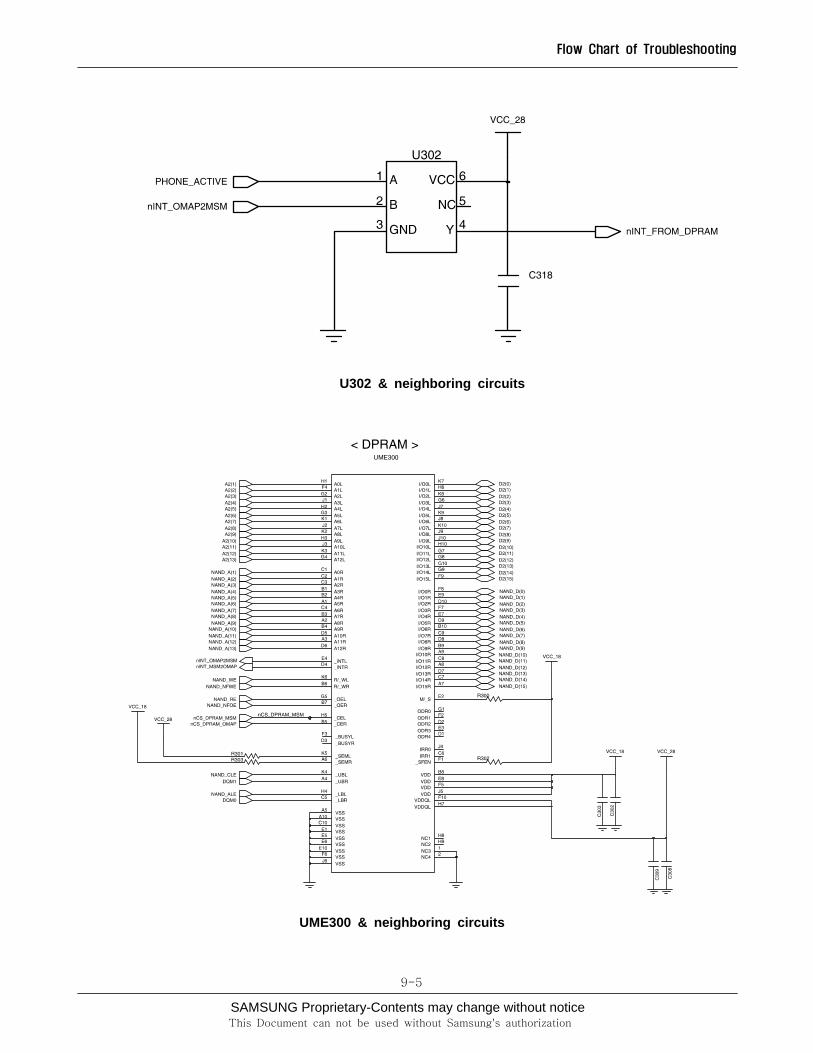
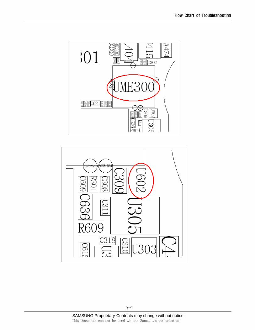
U302 & neighboring circuits
UME300 & neighboring circuits
SAMSUNG Proprietary-Contents may change without notice
Flow Chart of Troubleshooting
9-6
This Document can not be used without Samsung's authorization
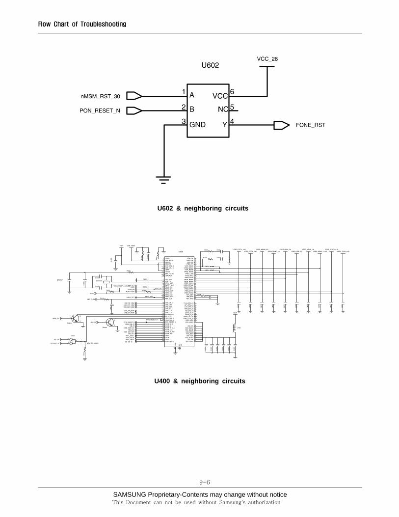
U602 & neighboring circuits
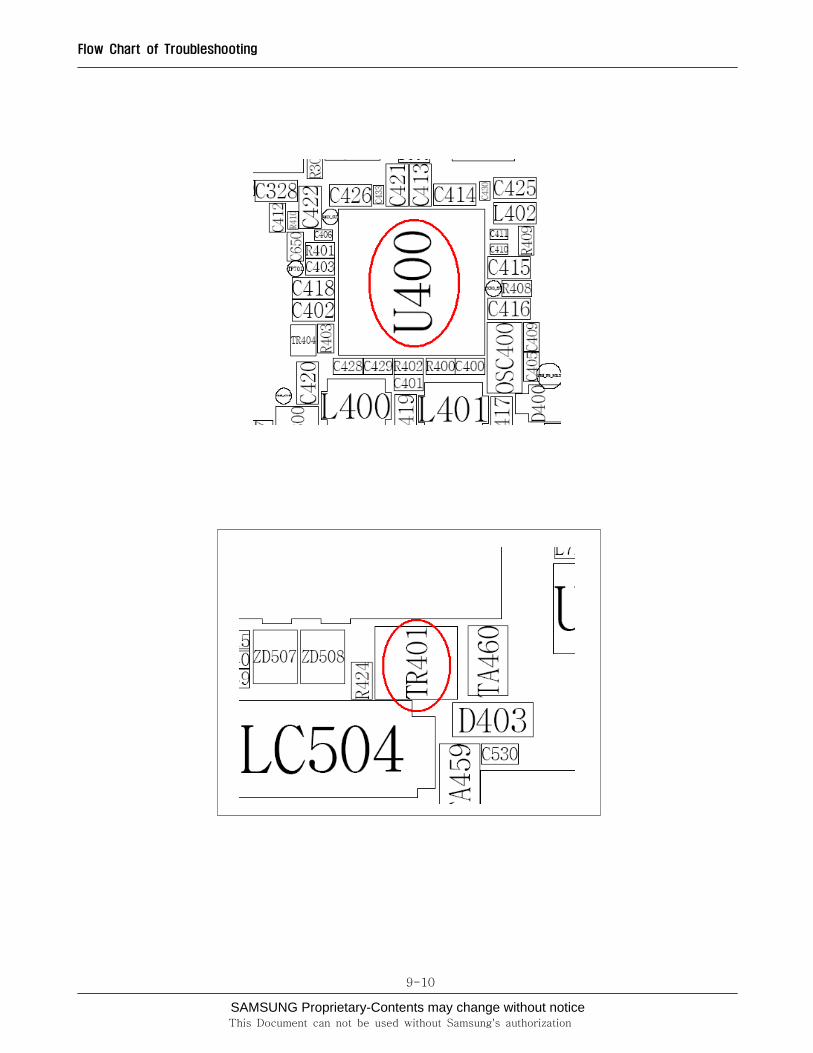
U400 & neighboring circuits
SAMSUNG Proprietary-Contents may change without notice
Flow Chart of Troubleshooting
9-7
This Document can not be used without Samsung's authorization
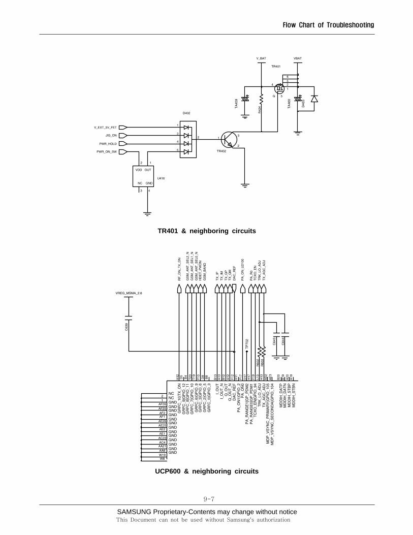
TR401 & neighboring circuits
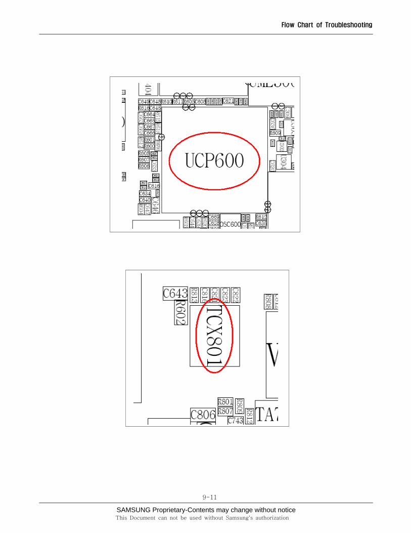
UCP600 & neighboring circuits
SAMSUNG Proprietary-Contents may change without notice
Flow Chart of Troubleshooting
9-8
This Document can not be used without Samsung's authorization
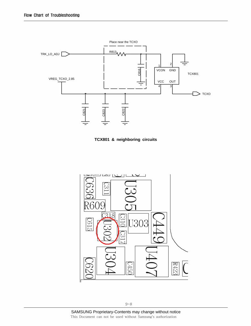
TCX801 & neighboring circuits
Place near the TCXO
1VCON
TCX801
2
GND
3OUTVCC
4C
821
C81
6
C82
3
VREG_TCXO_2.85
R813
C82
2
TRK_LO_ADJ
TCXO
SAMSUNG Proprietary-Contents may change without notice
Flow Chart of Troubleshooting
9-9
This Document can not be used without Samsung's authorization
SAMSUNG Proprietary-Contents may change without notice
Flow Chart of Troubleshooting
9-10
This Document can not be used without Samsung's authorization
SAMSUNG Proprietary-Contents may change without notice
Flow Chart of Troubleshooting
9-11
This Document can not be used without Samsung's authorization
SAMSUNG Proprietary-Contents may change without notice
Flow Chart of Troubleshooting
9-12
This Document can not be used without Samsung's authorization
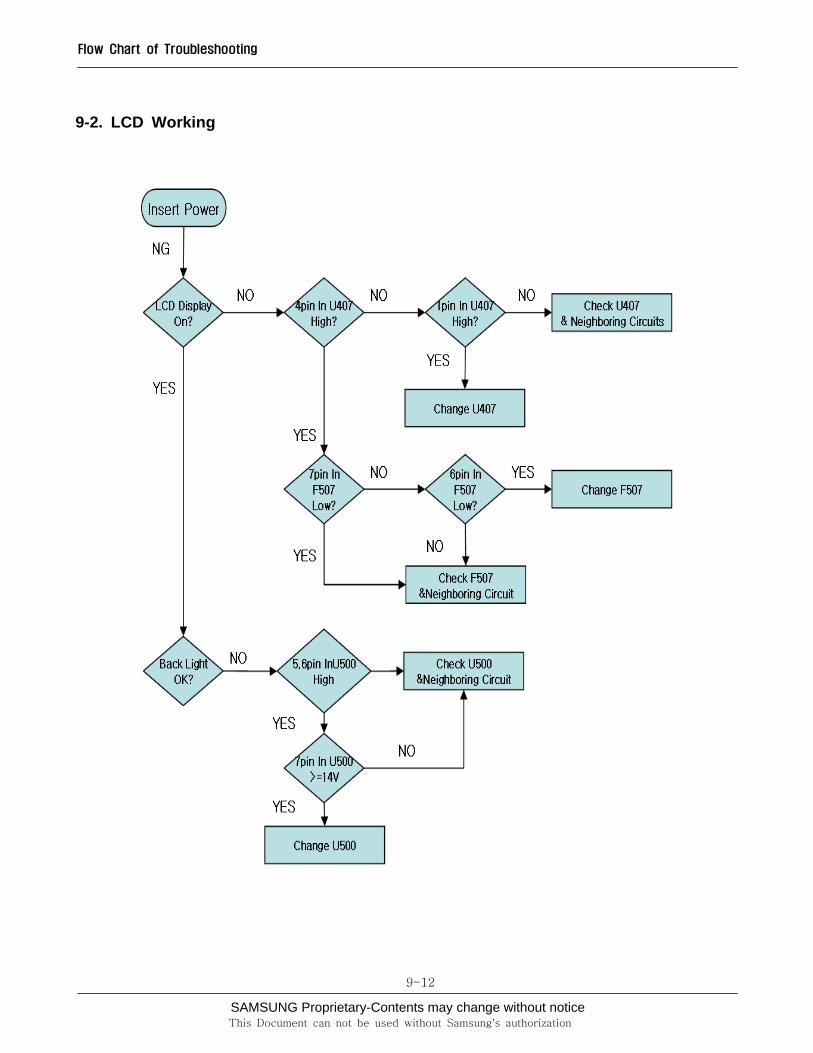
9-2. LCD Working
SAMSUNG Proprietary-Contents may change without notice
Flow Chart of Troubleshooting
9-13
This Document can not be used without Samsung's authorization
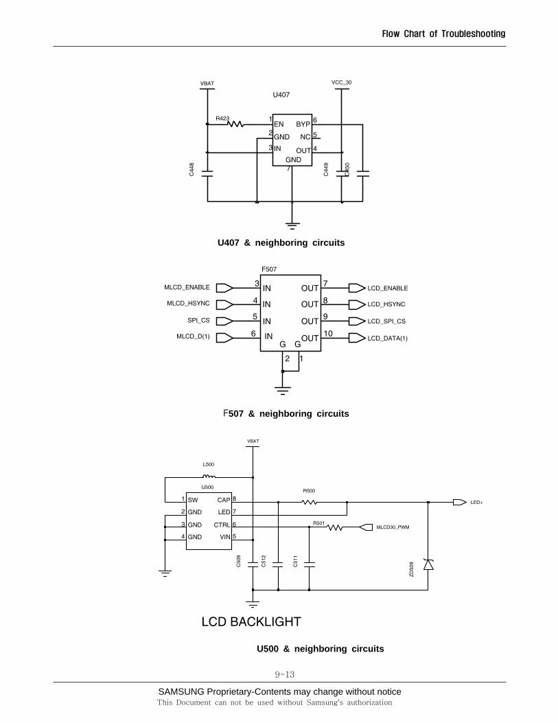
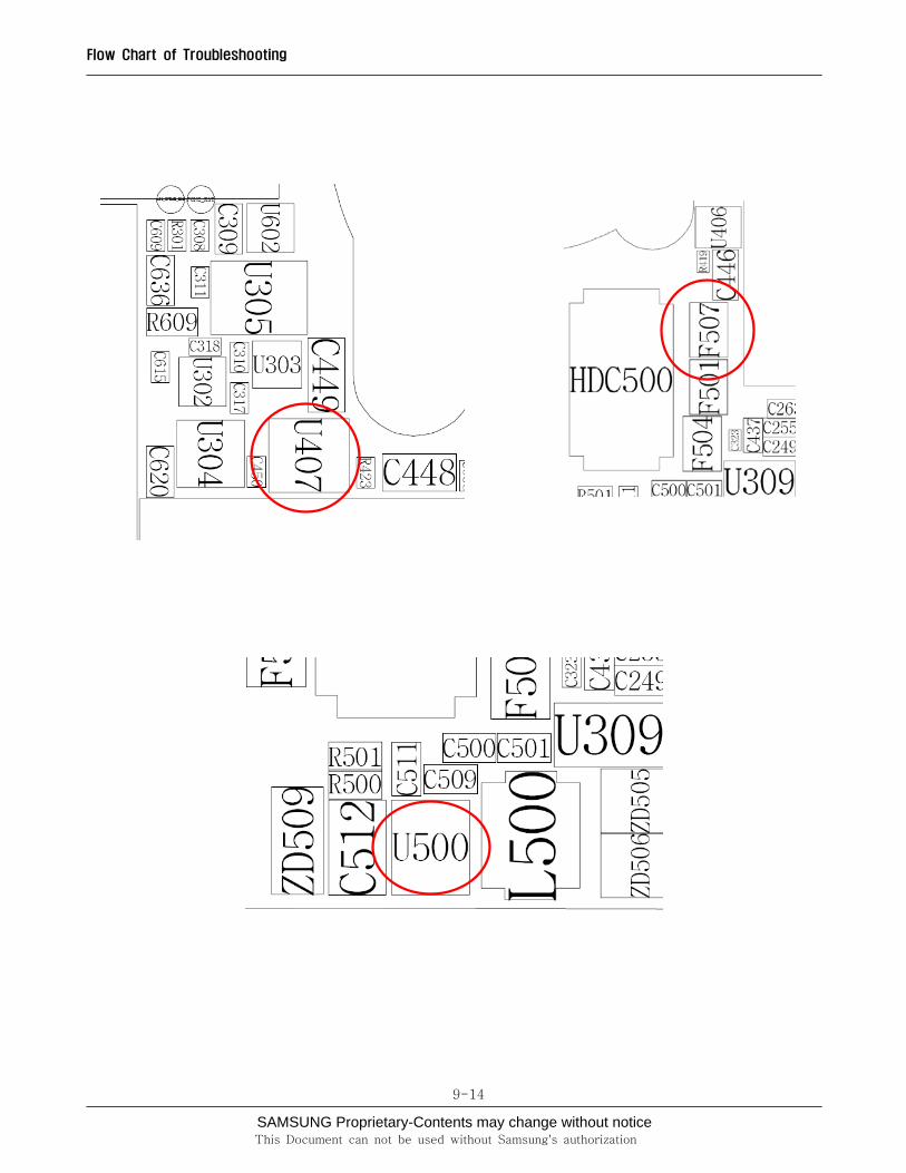
U407 & neighboring circuits
F507 & neighboring circuits
U500 & neighboring circuits
SAMSUNG Proprietary-Contents may change without notice
Flow Chart of Troubleshooting
9-14
This Document can not be used without Samsung's authorization
SAMSUNG Proprietary-Contents may change without notice
Flow Chart of Troubleshooting
9-15
This Document can not be used without Samsung's authorization
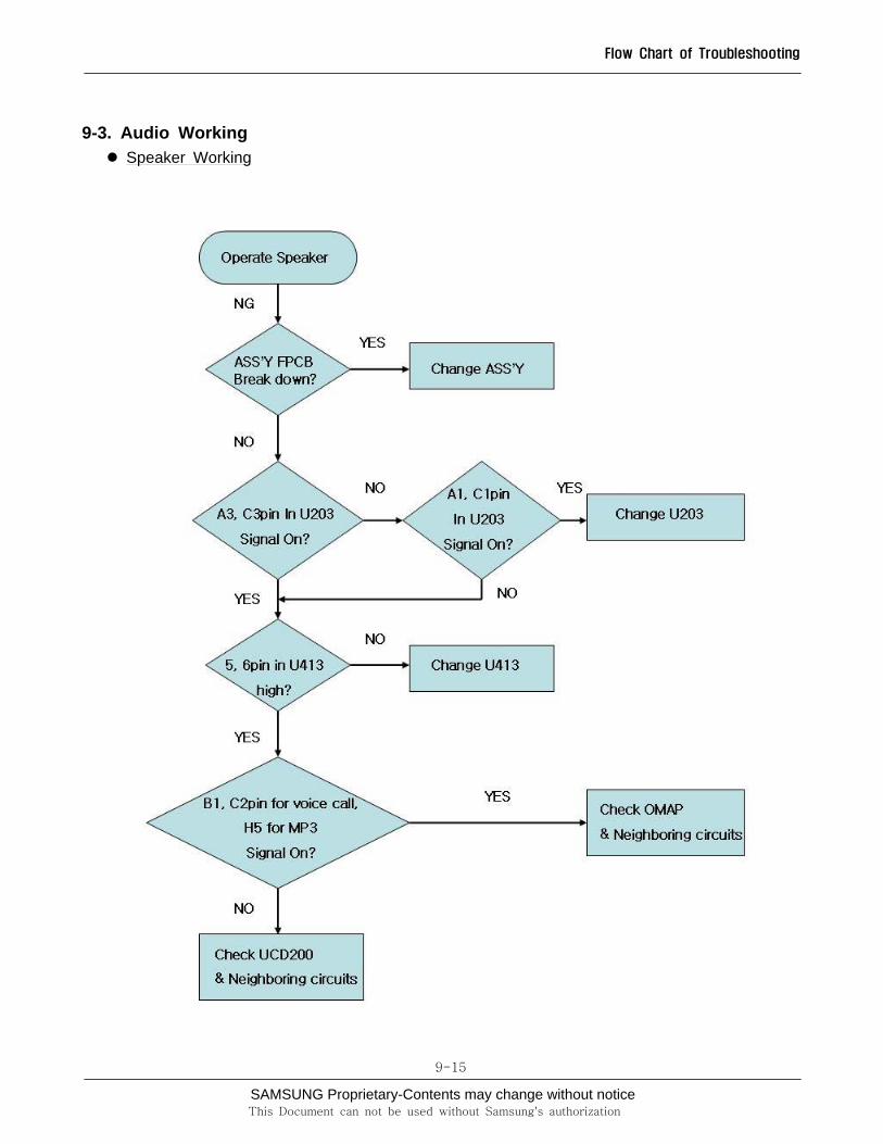
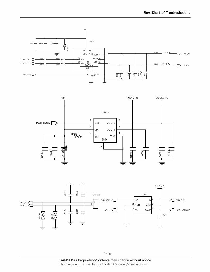
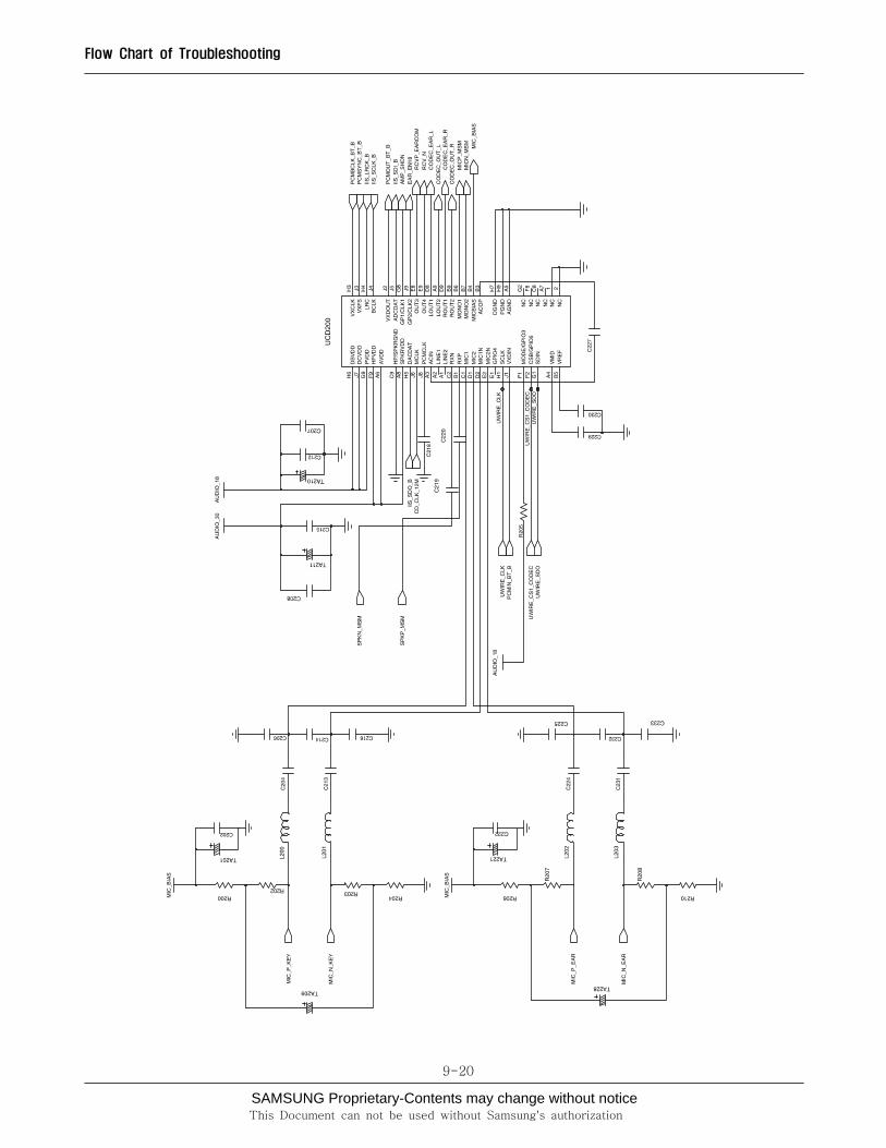
9-3. Audio WorkingSpeaker Working
SAMSUNG Proprietary-Contents may change without notice
Flow Chart of Troubleshooting
9-16
This Document can not be used without Samsung's authorization
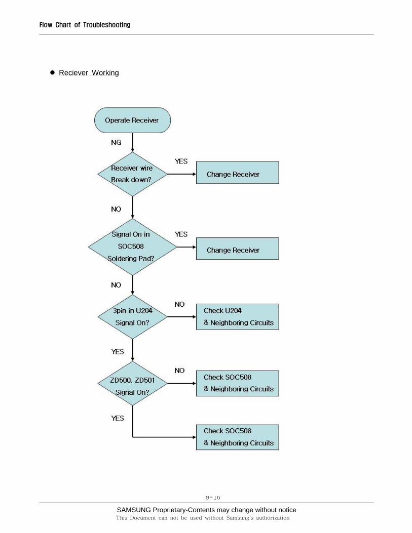
Reciever Working
SAMSUNG Proprietary-Contents may change without notice
Flow Chart of Troubleshooting
9-17
This Document can not be used without Samsung's authorization
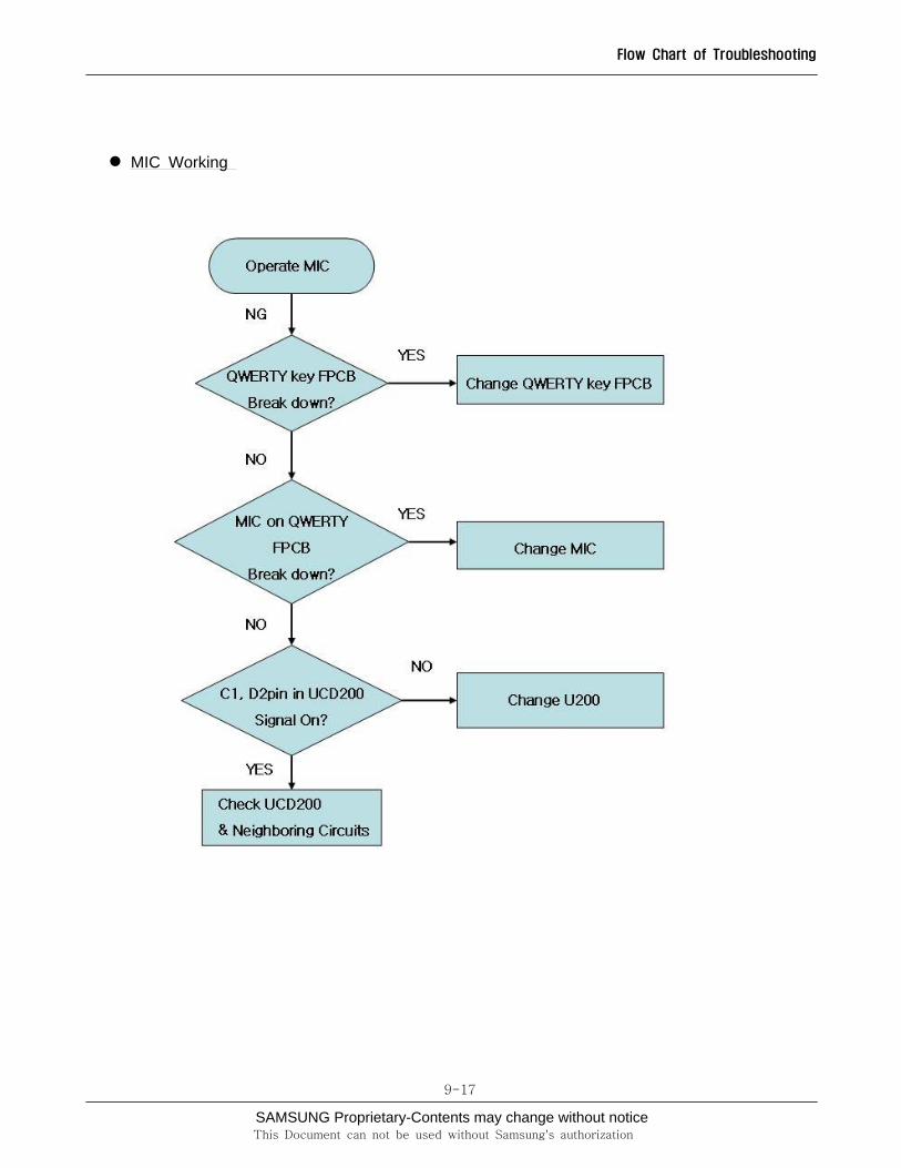
MIC Working
SAMSUNG Proprietary-Contents may change without notice
Flow Chart of Troubleshooting
9-18
This Document can not be used without Samsung's authorization
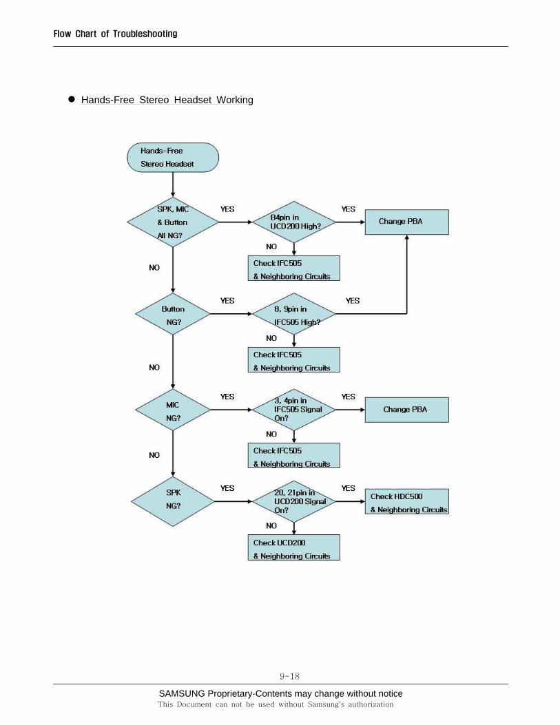
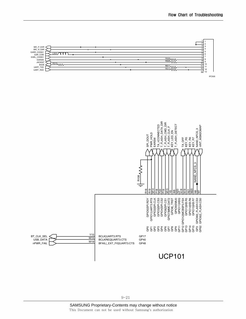
Hands-Free Stereo Headset Working
SAMSUNG Proprietary-Contents may change without notice
Flow Chart of Troubleshooting
9-19
This Document can not be used without Samsung's authorization
SAMSUNG Proprietary-Contents may change without notice
Flow Chart of Troubleshooting
9-20
This Document can not be used without Samsung's authorization
SAMSUNG Proprietary-Contents may change without notice
Flow Chart of Troubleshooting
9-21
This Document can not be used without Samsung's authorization
SAMSUNG Proprietary-Contents may change without notice
Flow Chart of Troubleshooting
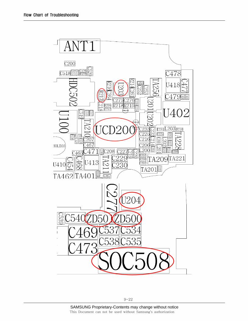
9-22
This Document can not be used without Samsung's authorization
SAMSUNG Proprietary-Contents may change without notice
Flow Chart of Troubleshooting
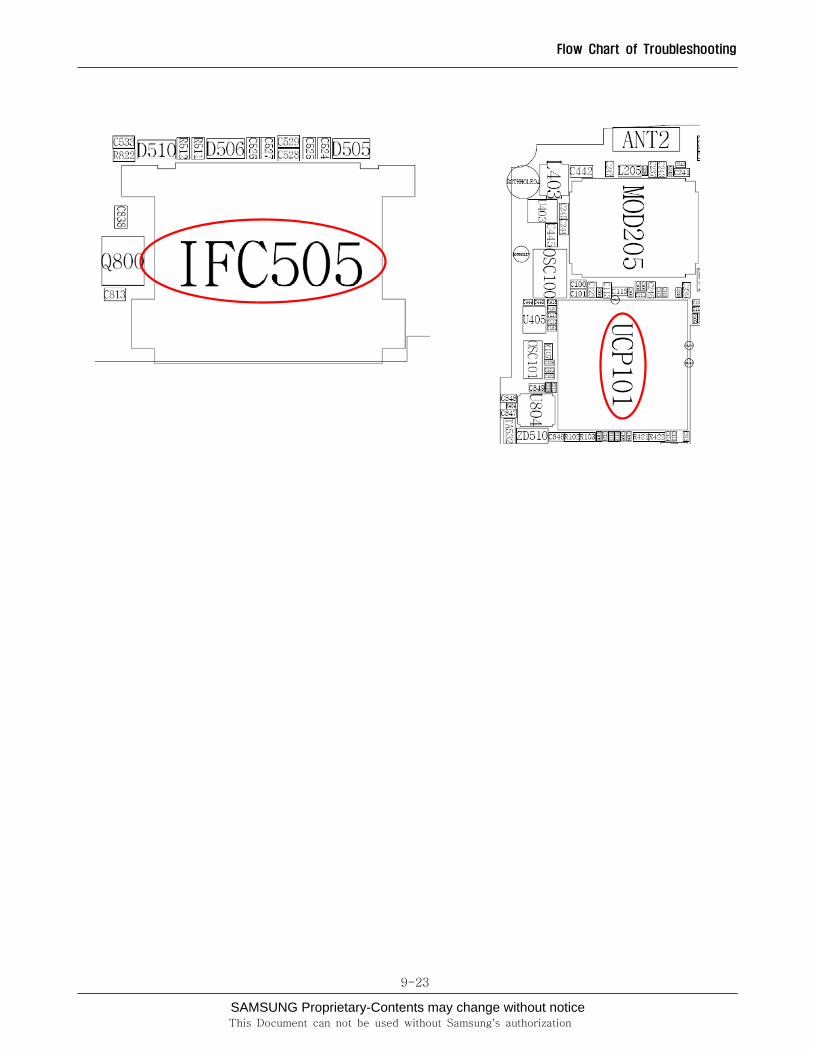
9-23
This Document can not be used without Samsung's authorization
SAMSUNG Proprietary-Contents may change without notice
Flow Chart of Troubleshooting
9-24
This Document can not be used without Samsung's authorization
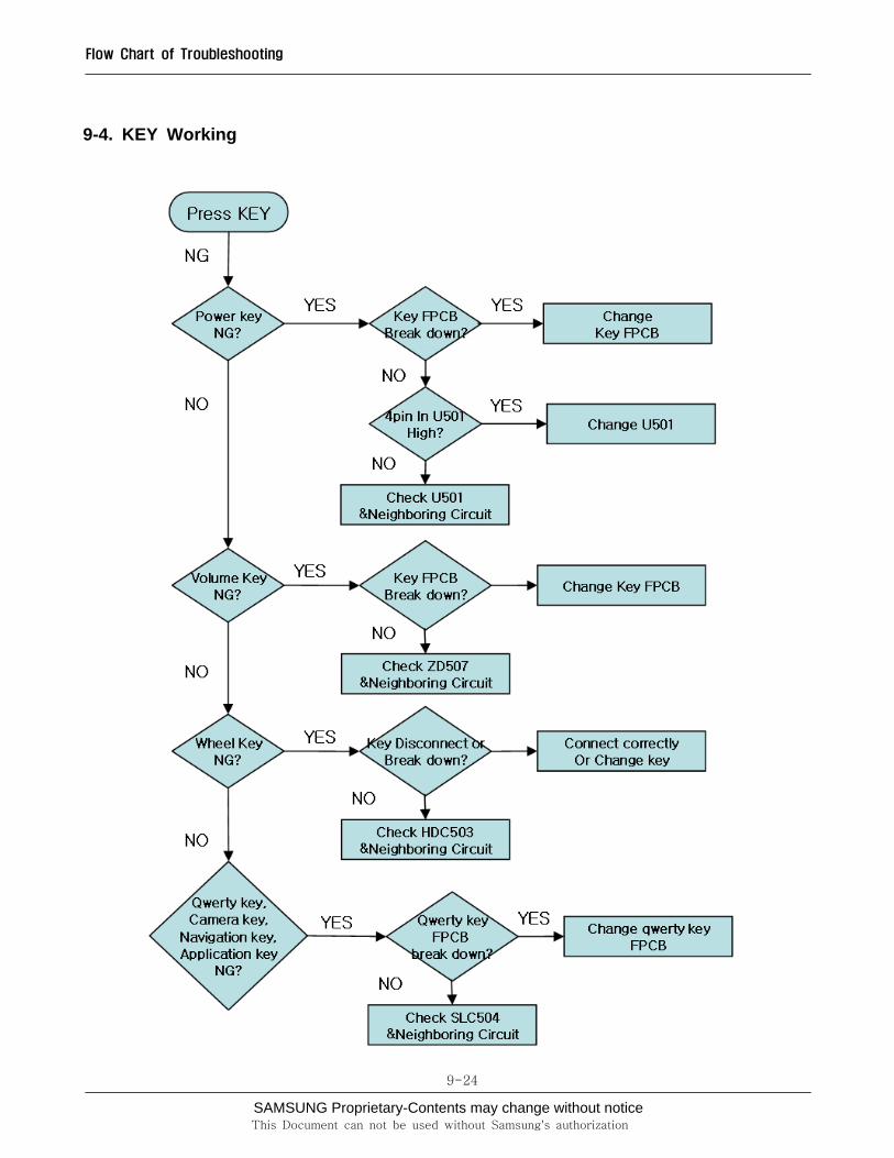
9-4. KEY Working
SAMSUNG Proprietary-Contents may change without notice
Flow Chart of Troubleshooting
9-25
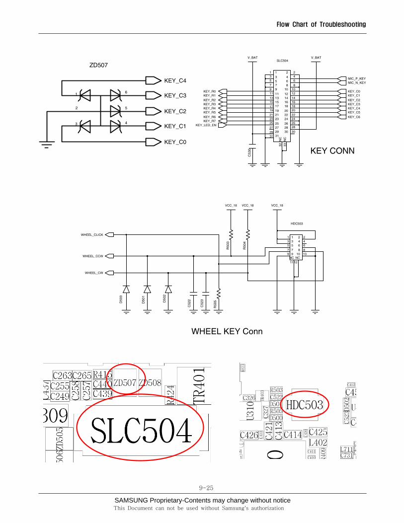
This Document can not be used without Samsung's authorization
SAMSUNG Proprietary-Contents may change without notice
Flow Chart of Troubleshooting
9-26
This Document can not be used without Samsung's authorization
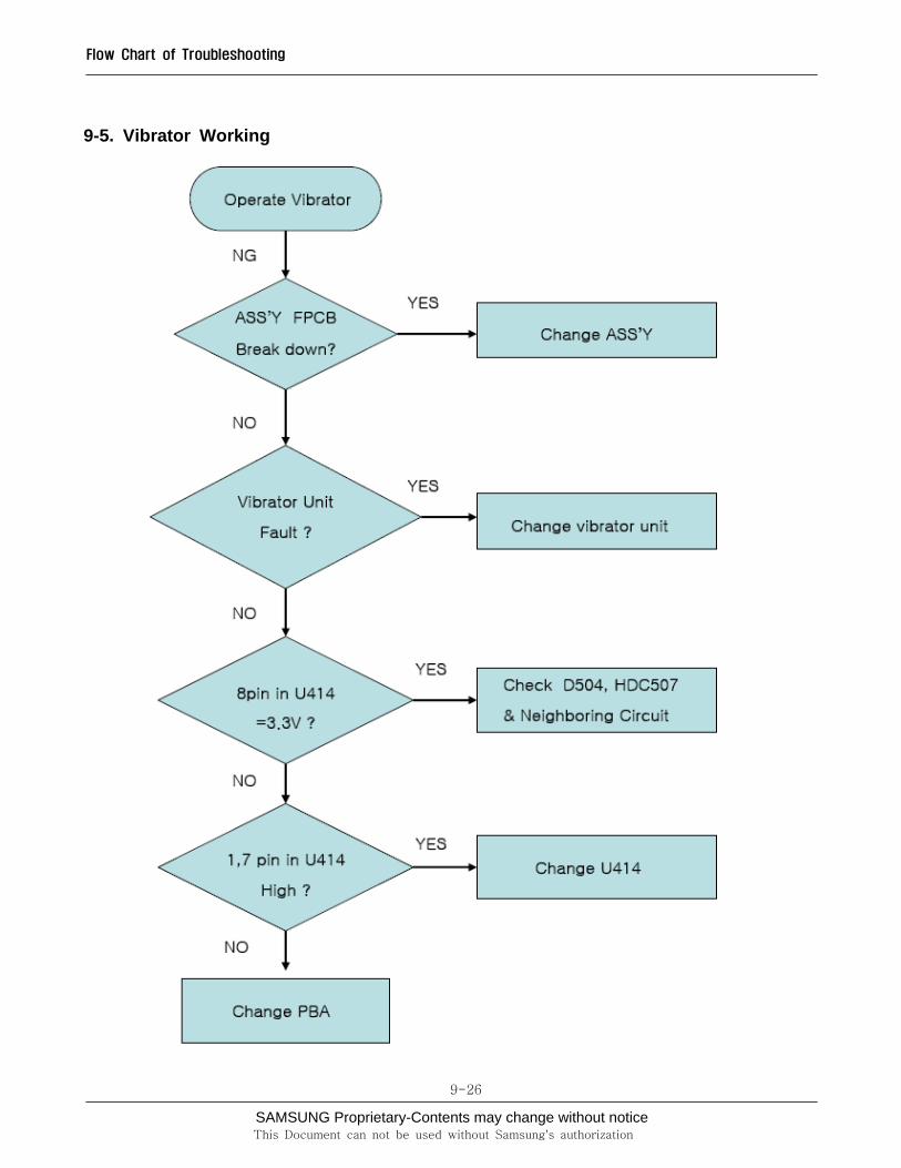
9-5. Vibrator Working
SAMSUNG Proprietary-Contents may change without notice
Flow Chart of Troubleshooting
9-27
This Document can not be used without Samsung's authorization
SAMSUNG Proprietary-Contents may change without notice
Flow Chart of Troubleshooting
9-28
This Document can not be used without Samsung's authorization
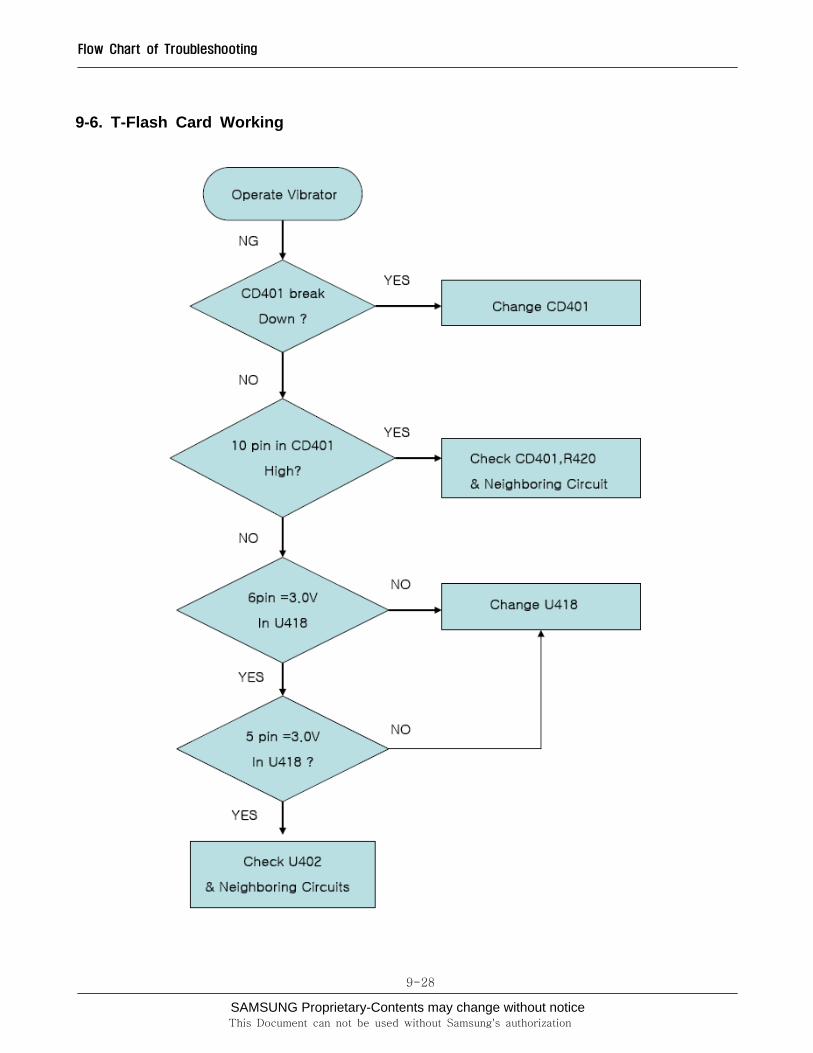
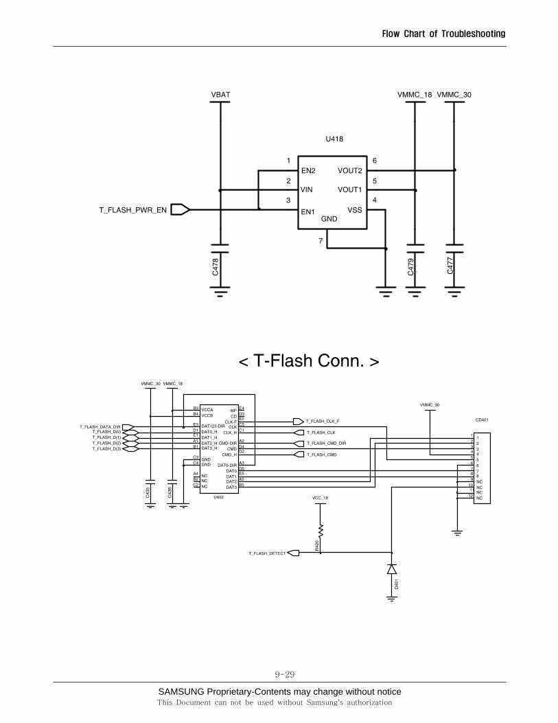
9-6. T-Flash Card Working
SAMSUNG Proprietary-Contents may change without notice
Flow Chart of Troubleshooting
9-29
This Document can not be used without Samsung's authorization
SAMSUNG Proprietary-Contents may change without notice
Flow Chart of Troubleshooting
9-30
This Document can not be used without Samsung's authorization
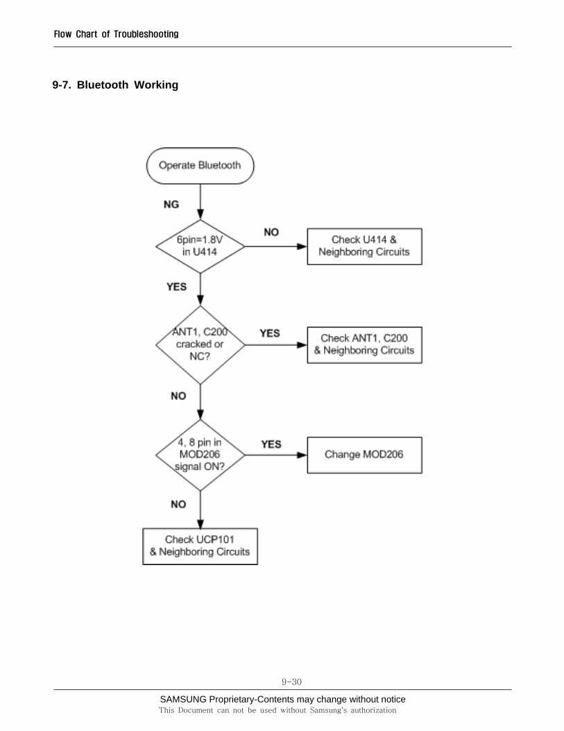
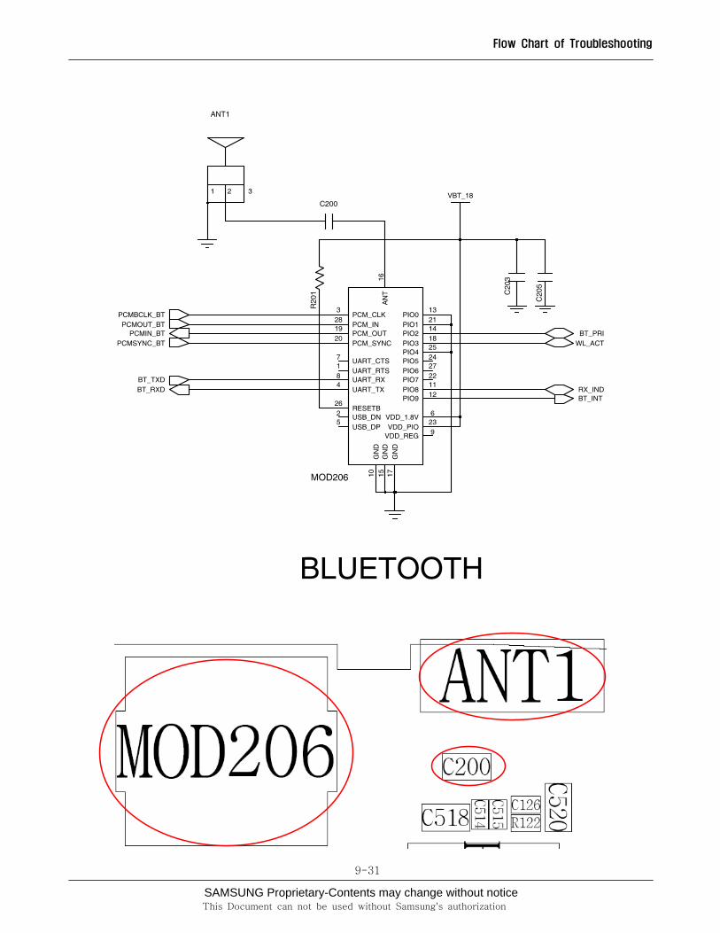
9-7. Bluetooth Working
SAMSUNG Proprietary-Contents may change without notice
Flow Chart of Troubleshooting
9-31
This Document can not be used without Samsung's authorization
SAMSUNG Proprietary-Contents may change without notice
Flow Chart of Troubleshooting
9-32
This Document can not be used without Samsung's authorization
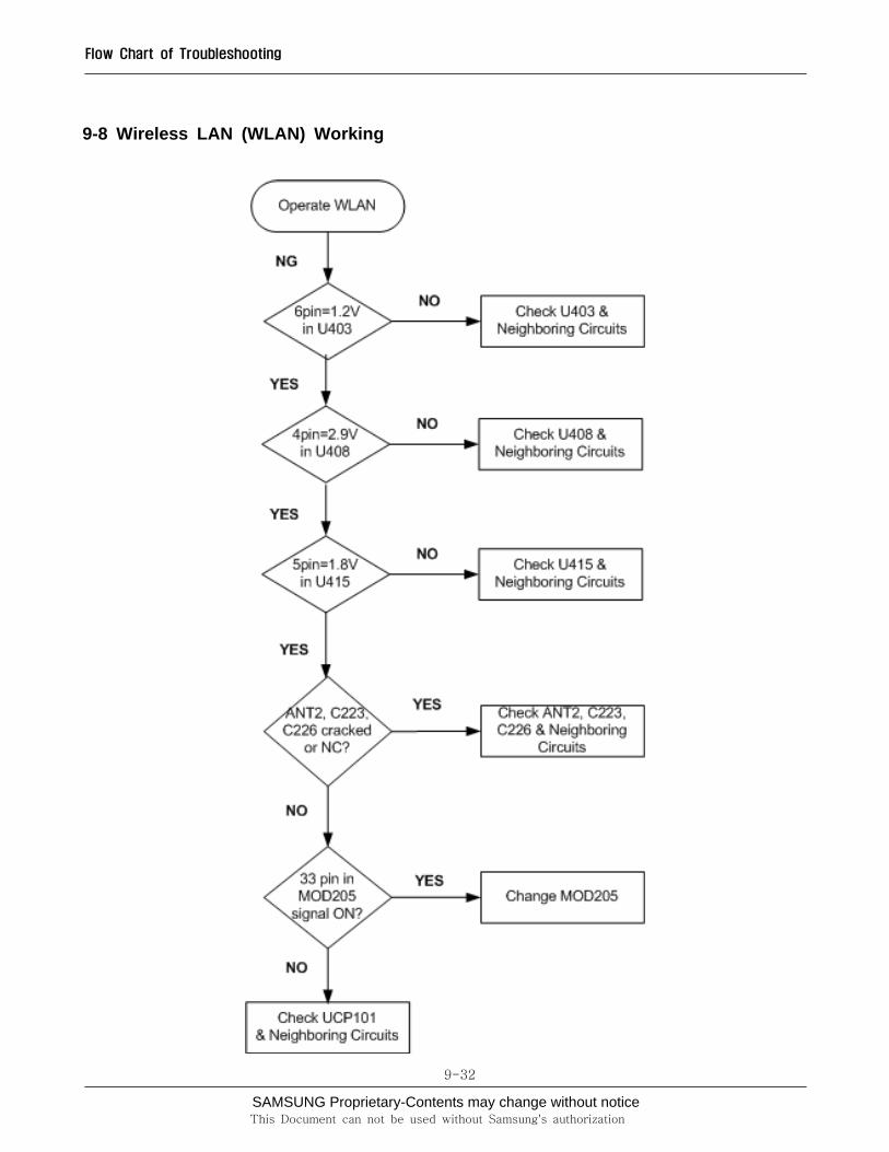
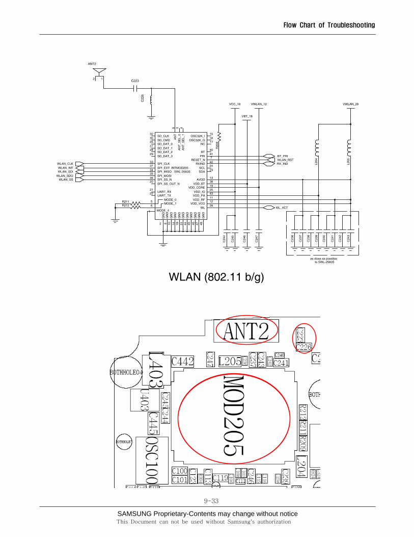
9-8 Wireless LAN (WLAN) Working
SAMSUNG Proprietary-Contents may change without notice
Flow Chart of Troubleshooting
9-33
This Document can not be used without Samsung's authorization
SAMSUNG Proprietary-Contents may change without notice
Flow Chart of Troubleshooting
9-34
This Document can not be used without Samsung's authorization
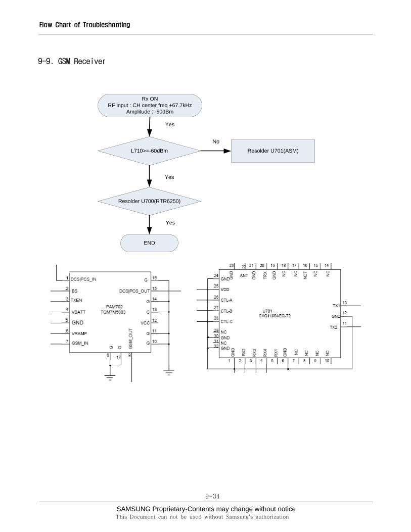
9-9. GSM Receiver
Rx ONRF input : CH center freq +67.7kHz
Amplitude : -50dBm
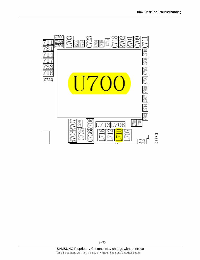
L710>=-60dBm Resolder U701(ASM)
Resolder U700(RTR6250)
END
Yes
No
Yes
Yes
SAMSUNG Proprietary-Contents may change without notice
Flow Chart of Troubleshooting
9-35
This Document can not be used without Samsung's authorization
SAMSUNG Proprietary-Contents may change without notice
Flow Chart of Troubleshooting
9-36
This Document can not be used without Samsung's authorization
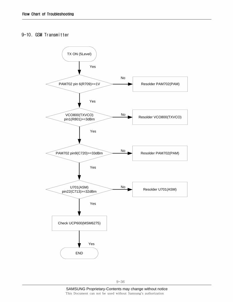
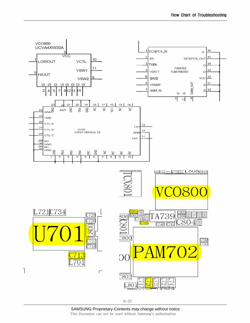
9-10. GSM Transmitter
TX ON (5Level)
PAM702 pin 6(R709)>=1V Resolder PAM702(PAM)
VCO800(TXVCO) pin1(R801)>=3dBm
END
Yes
No
Yes
Yes
Resolder VCO800(TXVCO)No
PAM702 pin9(C720)>=33dBm
Yes
Resolder PAM702(PAM)No
U701(ASM) pin22(C713)>=32dBm
Yes
Resolder U701(ASM)No
Check UCP600(MSM6275)
Yes
SAMSUNG Proprietary-Contents may change without notice
Flow Chart of Troubleshooting
9-37
This Document can not be used without Samsung's authorization
SAMSUNG Proprietary-Contents may change without notice
Flow Chart of Troubleshooting
9-38
This Document can not be used without Samsung's authorization
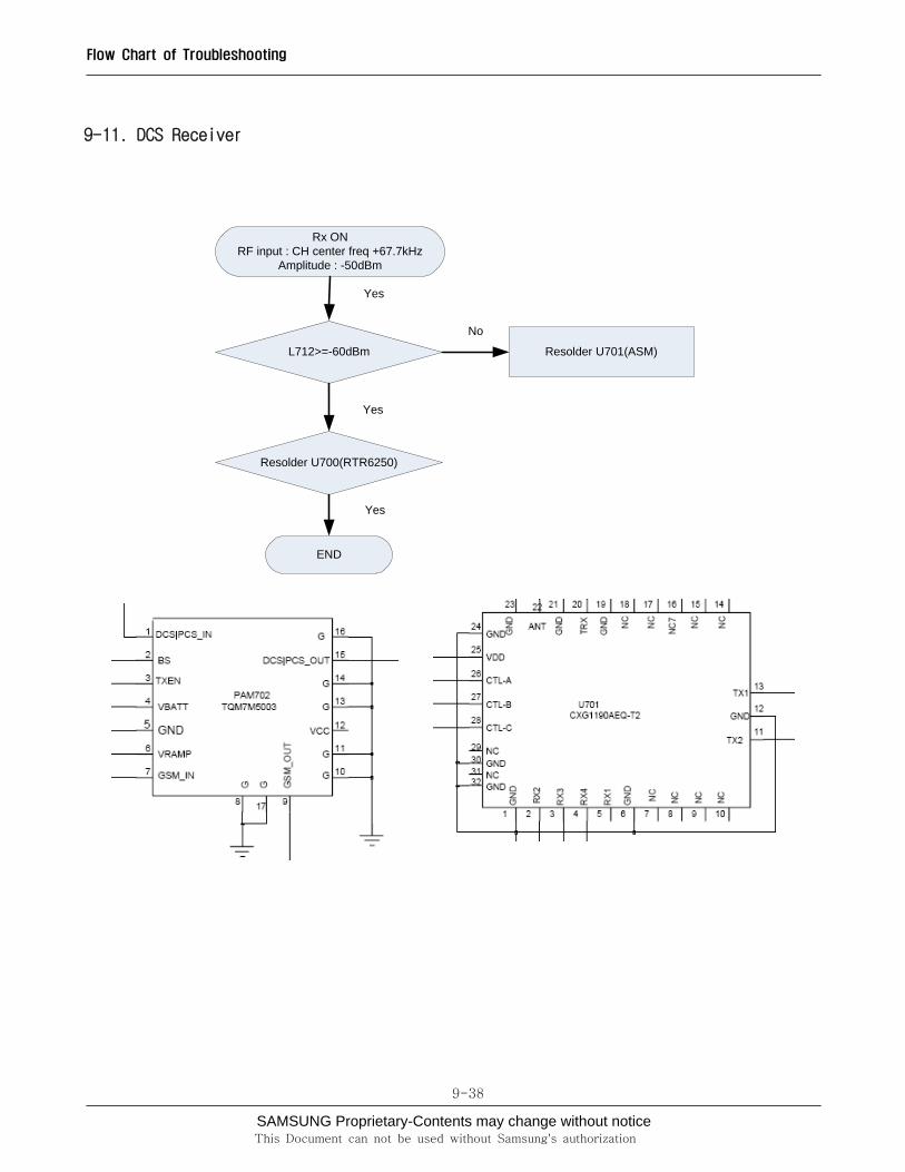
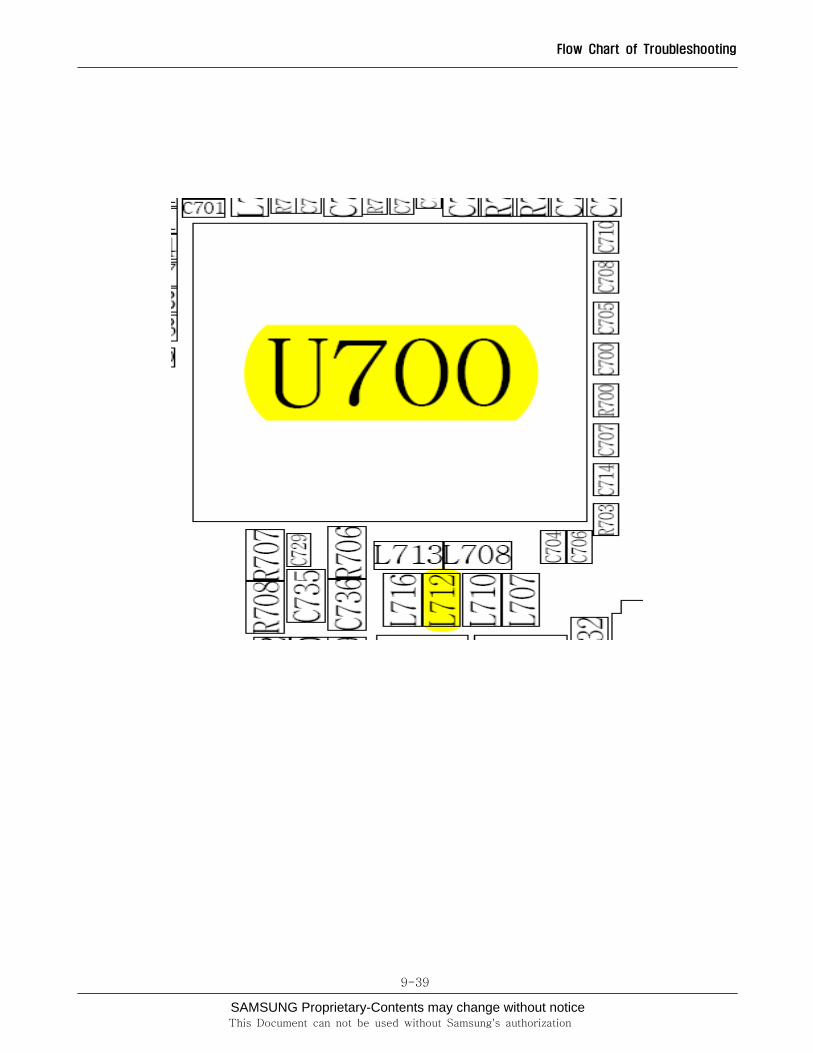
9-11. DCS Receiver
Rx ONRF input : CH center freq +67.7kHz
Amplitude : -50dBm
L712>=-60dBm Resolder U701(ASM)
Resolder U700(RTR6250)
END
Yes
No
Yes
Yes
SAMSUNG Proprietary-Contents may change without notice
Flow Chart of Troubleshooting
9-39
This Document can not be used without Samsung's authorization
SAMSUNG Proprietary-Contents may change without notice
Flow Chart of Troubleshooting
9-40
This Document can not be used without Samsung's authorization
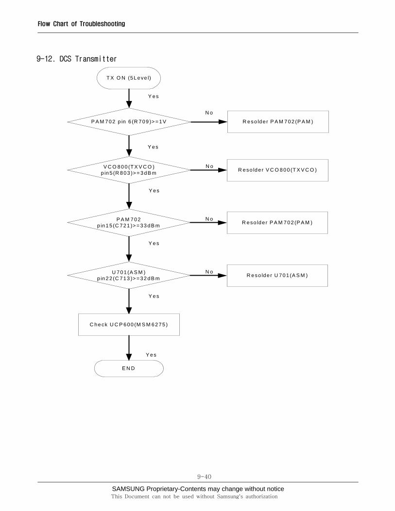
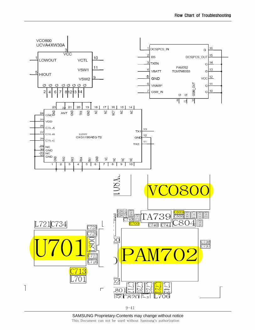
9-12. DCS Transmitter
T X O N (5Leve l)
P A M 7 02 p in 6 (R 709 )> = 1V R eso lde r P A M 7 02 (P A M )
V C O 80 0 (T X V C O ) p in 5 (R 803 )> = 3 dB m
E N D
Y es
N o
Y es
Y es
R eso lde r V C O 800 (T X V C O )N o
P A M 70 2 p in 1 5 (C 721 )> = 33 d B m
Y e s
R eso lde r P A M 70 2 (P A M )N o
U 701 (A S M ) p in 2 2 (C 713 )> = 32 d B m
Y e s
R eso lde r U 701 (A S M )N o
C heck U C P 600 (M S M 62 75 )
Y es
SAMSUNG Proprietary-Contents may change without notice
Flow Chart of Troubleshooting
9-41
This Document can not be used without Samsung's authorization
SAMSUNG Proprietary-Contents may change without notice
Flow Chart of Troubleshooting
9-42
This Document can not be used without Samsung's authorization
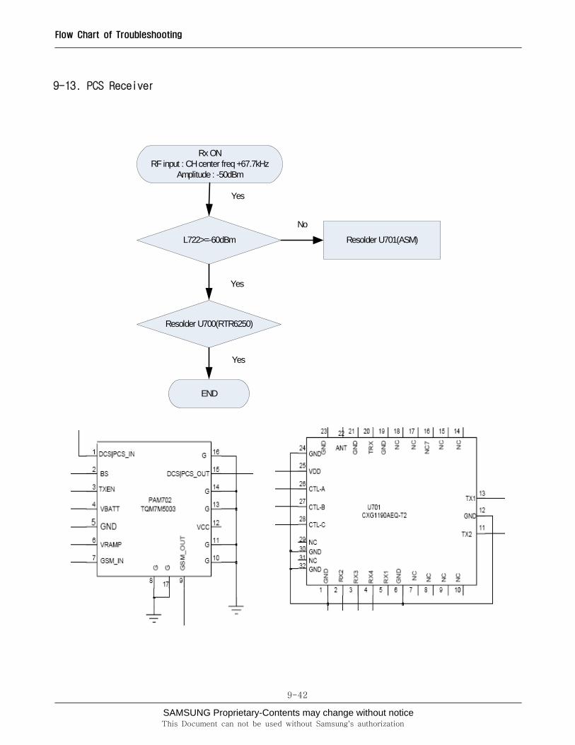
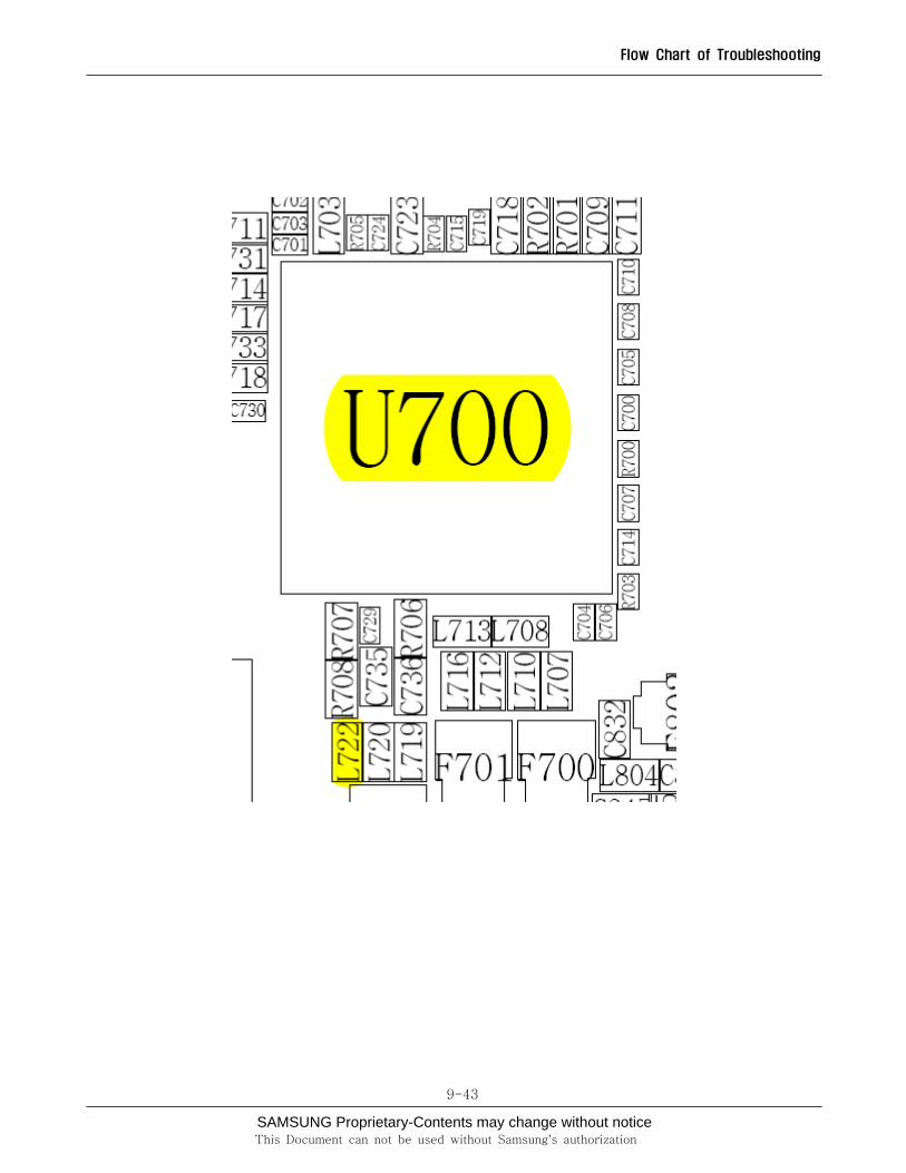
9-13. PCS Receiver
Rx ONRF input : CH center freq +67.7kHz
Amplitude : -50dBm
L722>=-60dBm Resolder U701(ASM)
Resolder U700(RTR6250)
END
Yes
No
Yes
Yes
SAMSUNG Proprietary-Contents may change without notice
Flow Chart of Troubleshooting
9-43
This Document can not be used without Samsung's authorization
SAMSUNG Proprietary-Contents may change without notice
Flow Chart of Troubleshooting
9-44
This Document can not be used without Samsung's authorization
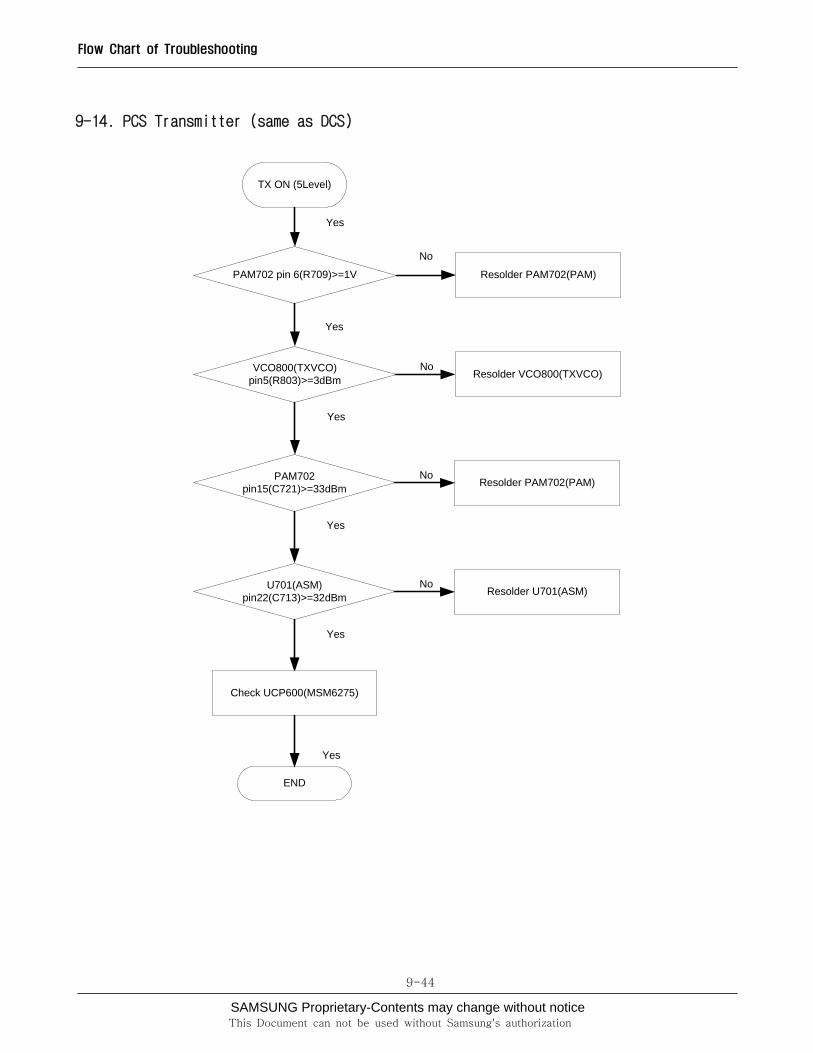
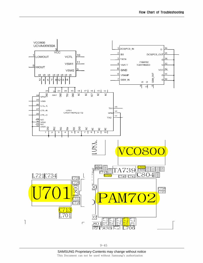
9-14. PCS Transmitter (same as DCS)
TX ON (5Level)
PAM702 pin 6(R709)>=1V Resolder PAM702(PAM)
VCO800(TXVCO) pin5(R803)>=3dBm
END
Yes
No
Yes
Yes
Resolder VCO800(TXVCO)No
PAM702 pin15(C721)>=33dBm
Yes
Resolder PAM702(PAM)No
U701(ASM) pin22(C713)>=32dBm
Yes
Resolder U701(ASM)No
Check UCP600(MSM6275)
Yes
SAMSUNG Proprietary-Contents may change without notice
Flow Chart of Troubleshooting
9-45
This Document can not be used without Samsung's authorization
SAMSUNG Proprietary-Contents may change without notice
Flow Chart of Troubleshooting
9-46
This Document can not be used without Samsung's authorization
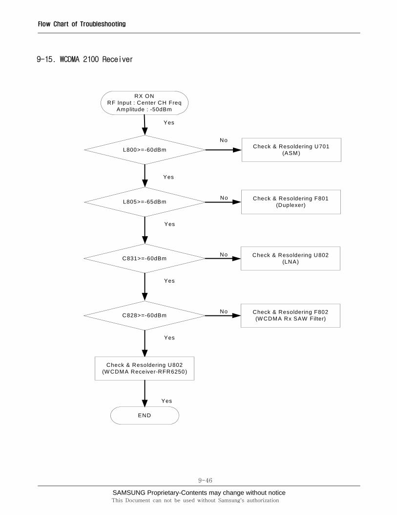
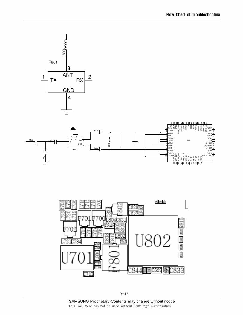
9-15. WCDMA 2100 Receiver
RX ONRF Input : Center CH Freq
Amplitude : -50dBm
L800>=-60dBm Check & Resoldering U701 (ASM)
L805>=-65dBm
END
Yes
No
Yes
Yes
Check & Resoldering F801 (Duplexer)
No
C831>=-60dBm
Yes
Check & Resoldering U802(LNA)
No
C828>=-60dBm
Yes
Check & Resoldering F802(W CDMA Rx SAW Filter)
No
Check & Resoldering U802(WCDMA Receiver-RFR6250)
Yes
SAMSUNG Proprietary-Contents may change without notice
Flow Chart of Troubleshooting
9-47
This Document can not be used without Samsung's authorization
SAMSUNG Proprietary-Contents may change without notice
Flow Chart of Troubleshooting
9-48
This Document can not be used without Samsung's authorization
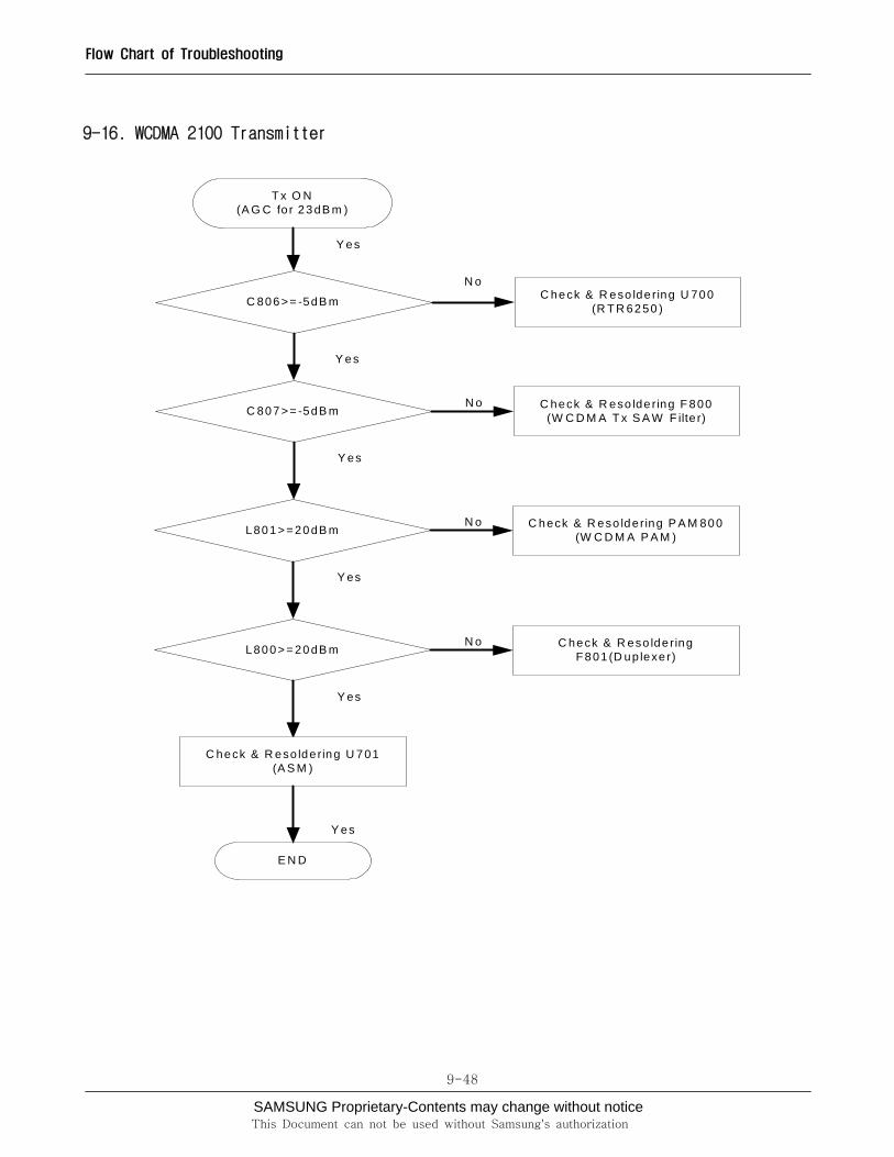
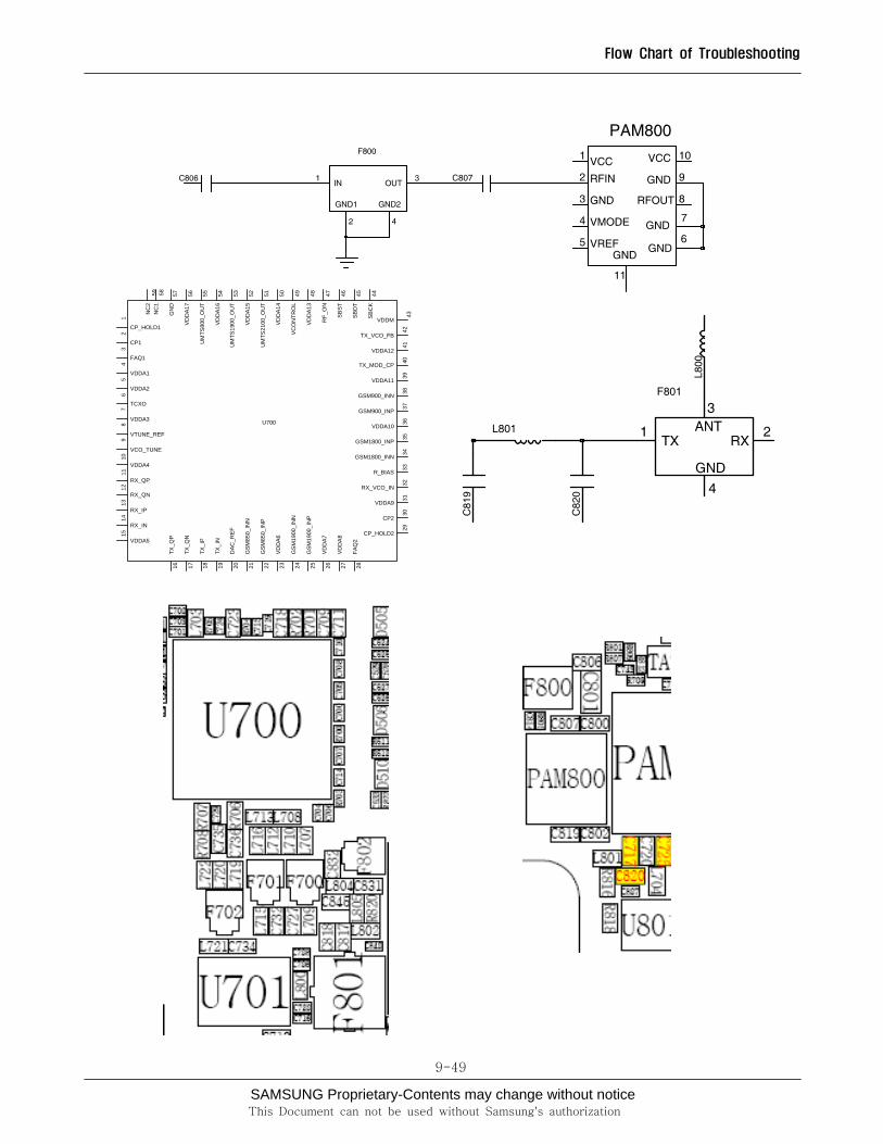
9-16. WCDMA 2100 Transmitter
T x O N(A G C fo r 23 dB m )
C 806 >= -5dB m C heck & R eso lde ring U 700 (R T R 6250 )
C 807 >= -5dB m
E N D
Y es
N o
Y es
Y es
C heck & R eso lde ring F 800 (W C D M A T x S A W F ilte r)
N o
L801 > = 20 dB m
Y es
C heck & R eso ldering P A M 800(W C D M A P A M )
N o
L800 > = 20 dB m
Y es
C heck & R eso lde ring F 801 (D up lexe r)
N o
C heck & R eso lde ring U 701(A S M )
Y es
SAMSUNG Proprietary-Contents may change without notice
Flow Chart of Troubleshooting
9-49
This Document can not be used without Samsung's authorization
87
VDDA4
10
VDDA5
15
VDD
A623
VDD
A726 27
VDD
A8
VDDA9 3143
VDDM
VTUNE_REF
39
VDDA12
41
VDD
A13
48
VDD
A14
50
VDD
A15
5254VD
DA1
6
VDD
A17
56
5
VDDA2
VDDA3
42
UM
TS19
00_O
UT
53
UM
TS21
00_O
UT
51
UM
TS80
0_O
UT
55
VC
ON
TRO
L49
9
VCO_TUNE
VDDA1
4
36VDDA10
VDDA11
45
SBST
46
TCXO
6
TX_I
N19
TX_I
P18
40TX_MOD_CP
TX_Q
N1716
TX_Q
P
TX_VCO_FB47
RX_IN
14
RX_IP
13
RX_QN
12
RX_QP
11
32RX_VCO_IN
R_BIAS 33
44S
BCK
SBD
T
24
GSM
1900
_IN
P25
GSM
850_
INN
21
GSM
850_
INP
22
GSM900_INN 3837GSM900_INP
NC
15859
NC
2
RF_
ON
1
CP_HOLD2
29
DAC
_REF
20
FAQ1
3
FAQ
228
57G
ND
GSM1800_INN 3435GSM1800_INP
GS
M19
00_I
NN
U700
CP1
2
30
CP2
CP_HOLD1
SAMSUNG Proprietary-Contents may change without notice
Flow Chart of Troubleshooting
9-50
This Document can not be used without Samsung's authorization
SAMSUNG Proprietary-Contents may change without notice
10. Reference data
10-1
This Document can not be used without Samsung's authorization
Reference Abbreviate
― ARFCN : Absolute Radio Frequency Channel Number― BGA : Ball Grid Array― DCS : Digital Communications System― DL : Downlink― EFS : Embaded File System― EGSM : Enhanced Global System for Mobile Communications― FTP : File Transfer Protocol― HPSK : Hybrid Phase Shift Keying― Mcps : Mega-chips per second― MMS : Multimedia Messaging Service― MSK : Minimum Shift Keying― OBEX : OBject EXchange― PBA : Panel Board Assembly― PCS : Personal Communication System― PIM(S) : Personal Information Management (System)― QPSK : Quadrature Phase Shift Keying― RNDIS : Remote Network Driver Interface Specification― RSS : Received Signal Strength― SAW : Surface Acoustic Wave― SMS : Short Message Service― UL : Uplink― USB : Universal Serial Bus― WCDMA : Wideband Code Division Multiple Access
SAMSUNG Proprietary-Contents may change without notice
Reference data
10-2
This Document can not be used without Samsung's authorization
Recommended