Robert Colville Team
Team Members Noah Boydston Kyle Brown Robert Colville Linsy Cook GeeHyun Park Wissam Khazem

Applications of Bipolar Transistors
Bipolar Transistors verses MOS Advantages
High Transconductance Directly Proportional to Emitter current Independent of emitter area Improves base-emitter voltage matching
Superior device matching Resulting bipolar applications
High output applications – amplifiers, output drivers Precision output applications – voltage regulators,
voltage and current references
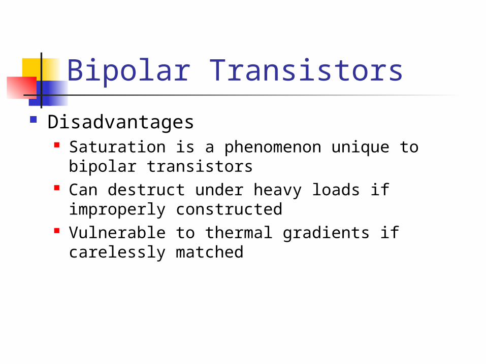
Bipolar Transistors Disadvantages
Saturation is a phenomenon unique to bipolar transistors
Can destruct under heavy loads if improperly constructed
Vulnerable to thermal gradients if carelessly matched

Power Bipolar Transistors Must increase emitter area to accommodate
large currents -- exceeding device’s critical current density results in beta degradation
Power transistors operate at lower betas to conserve space. Typical beta minimum is 10.
NPN transistors can handle higher currents so they are used more often than PNP transistors
Transistors handling currents over 100mA require special layouts to avoid thermal runaway and secondary breakdown

Power Bipolar Transistors Integrated bipolar transistors have
practical maximum current/power limit of 2 A and 10 W
Beyond this range, discrete components are more practical than integrated components
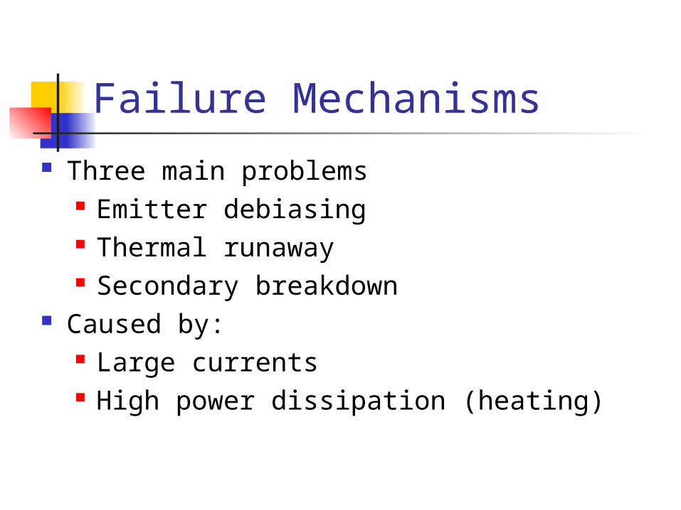
Failure Mechanisms Three main problems
Emitter debiasing Thermal runaway Secondary breakdown
Caused by: Large currents High power dissipation (heating)
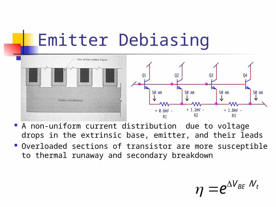
Emitter Debiasing
A non-uniform current distribution due to voltage drops in the extrinsic base, emitter, and their leads
Overloaded sections of transistor are more susceptible to thermal runaway and secondary breakdown
Q4
50 mA
R1+ 0.6mV -
R3+ 1.8mV -
Q3
50 mA
R2+ 1.2mV -
Q1
50 mA
Q2
50 mA
tBE VVe /
Emitter Ballasting Resistors inserted into each emitter lead Sized to provide voltage drop of 50 to 75mV Forces the emitter current to distribute more evenly Disadvantage: Voltage drop across resistors
adds to saturation voltage, lowers transconductance, and increases power dissipation
RB4
R2
Q3
RB3
Q4
RB1 RB2
Q1
R1 R3
Q2
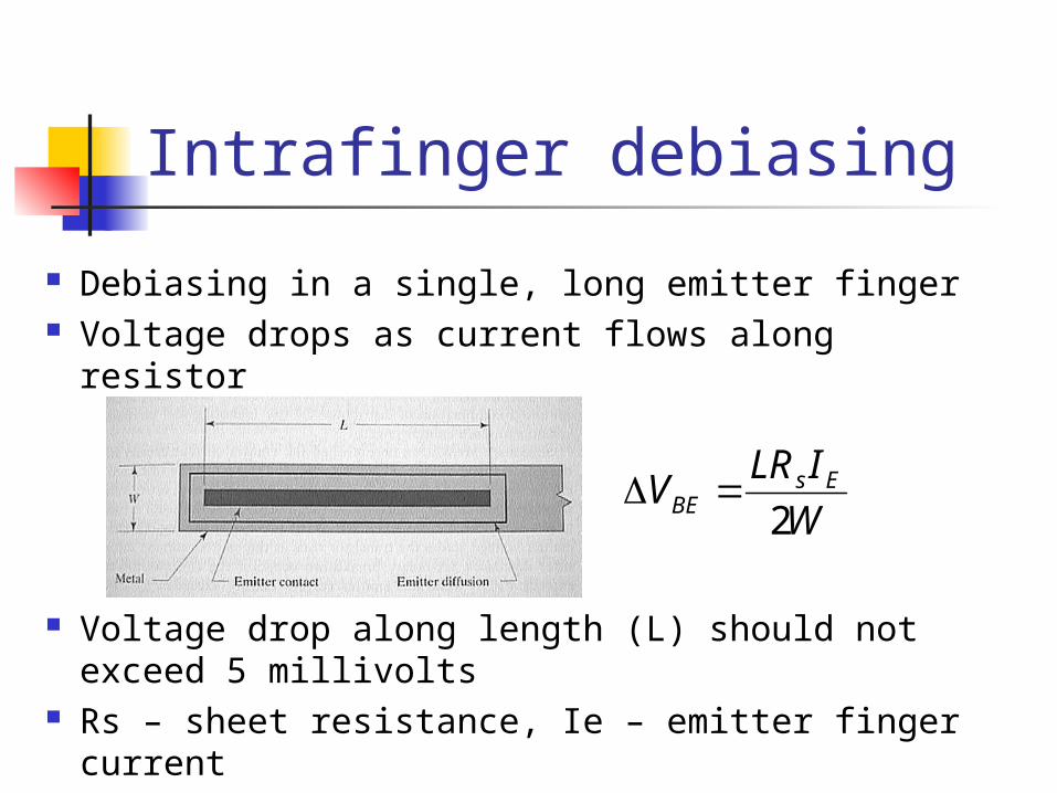
Intrafinger debiasing
Debiasing in a single, long emitter finger Voltage drops as current flows along resistor
Voltage drop along length (L) should not exceed 5 millivolts
Rs – sheet resistance, Ie – emitter finger current
W
ILRV EsBE 2
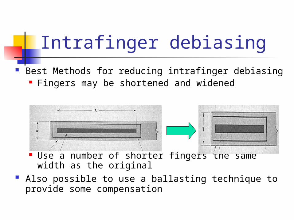
Intrafinger debiasing Best Methods for reducing intrafinger debiasing
Fingers may be shortened and widened
Use a number of shorter fingers the same width as the original
Also possible to use a ballasting technique to provide some compensation
Thermal Runaway Localized current flow as transistor heats
unevenly VBE drops by 2mV / °C Conduction region can quickly collapse to form
small hot spot Can cause catastrophic failure Overstress leads to other failures
Prevention Ballasting resistors to lessen debiasing Distributed emitter ballasting
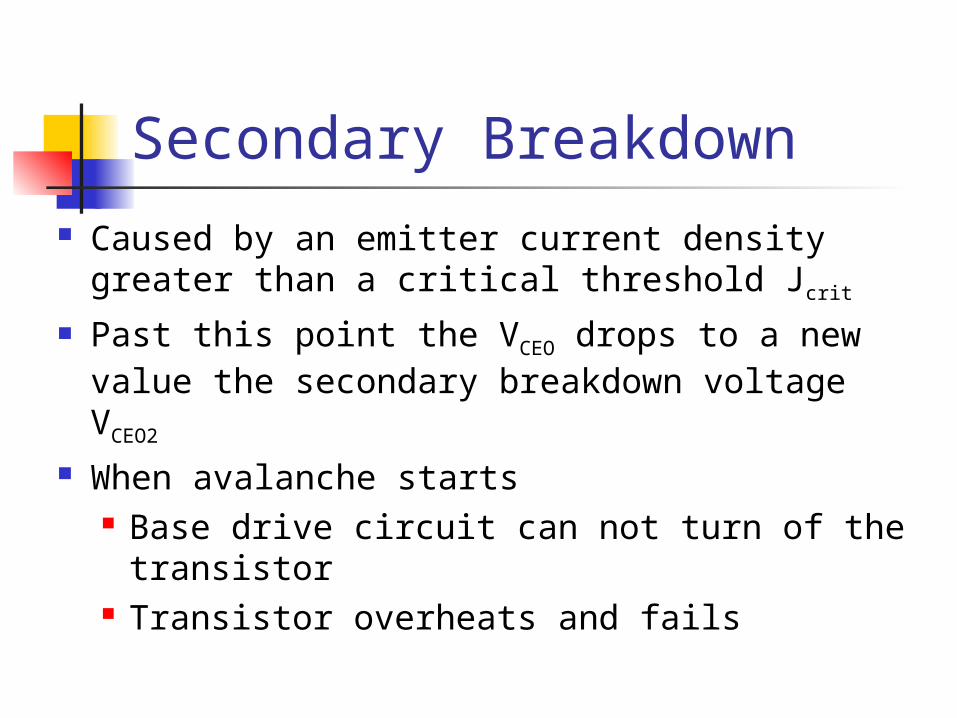
Secondary Breakdown Caused by an emitter current density
greater than a critical threshold Jcrit
Past this point the VCEO drops to a new value the secondary breakdown voltage VCEO2
When avalanche starts Base drive circuit can not turn of the
transistor Transistor overheats and fails
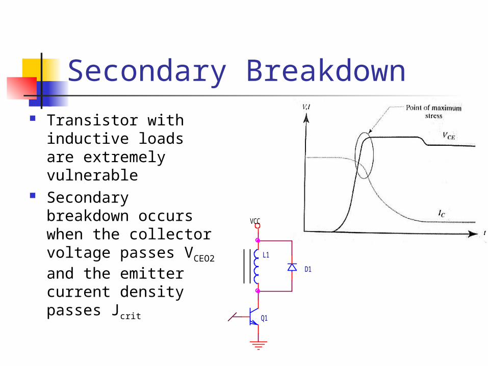
Secondary Breakdown Transistor with
inductive loads are extremely vulnerable
Secondary breakdown occurs when the collector voltage passes VCEO2 and the emitter current density passes Jcrit
D1
Q1
L1
VCC

Layout of Power NPN Transistors
Several types of layout designs Transistors used in linear-mode applications
Heat dissipation Transistors used in switch-mode
applications Emitter focusing
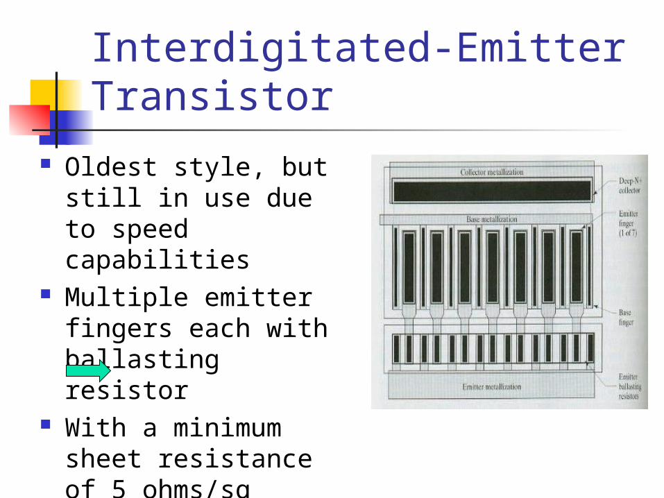
Interdigitated-Emitter Transistor
Oldest style, but still in use due to speed capabilities
Multiple emitter fingers each with ballasting resistor
With a minimum sheet resistance of 5 ohms/sq
Ballasting resistance of 2.5 ohms/sq per finger
Interdigitated-Emitter Transistor
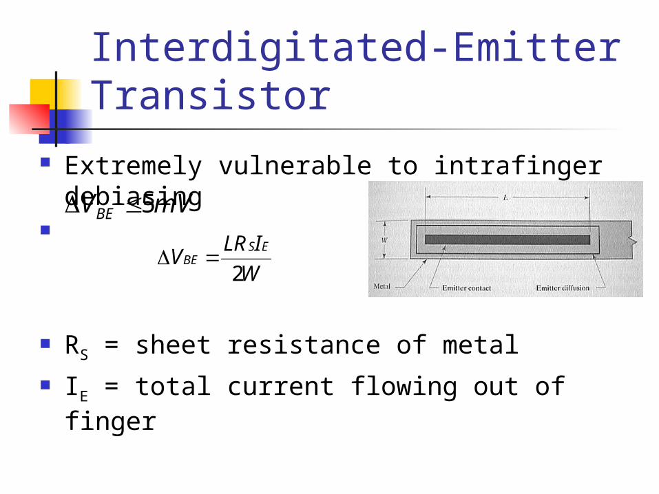
Extremely vulnerable to intrafinger debiasing
RS = sheet resistance of metal IE = total current flowing out of finger
W
ILRV
ESBE
2
mVVBE 5
Interdigitated Emitter Transistor
Design Considerations Large number of shortened fingers Increased width
Slower switching, emitter focusing Fastest designs use minimum-width
fingers Difficult to place enough metal on
narrow fingers to prevent them from debiasing
W
ILRV
ESBE
2
Interdigitated Emitter Transistor
Design Compromises Emitter width of 8 to 25 um Contacts as large as possible
Reduce emitter resistance
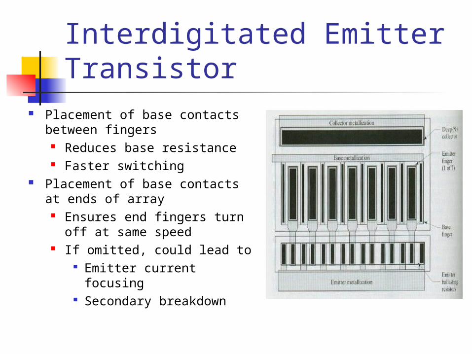
Interdigitated Emitter Transistor
Placement of base contacts between fingers
Reduces base resistance Faster switching
Placement of base contacts at ends of array
Ensures end fingers turn off at same speed
If omitted, could lead to Emitter current focusing Secondary breakdown
Interdigitated Emitter Transistor
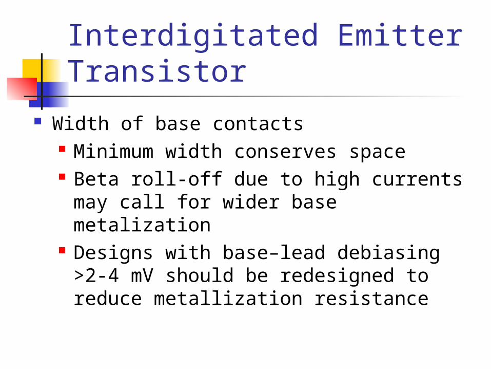
Width of base contacts Minimum width conserves space Beta roll-off due to high currents may call
for wider base metalization Designs with base–lead debiasing >2-4
mV should be redesigned to reduce metallization resistance
Interdigitated Emitter Transistor
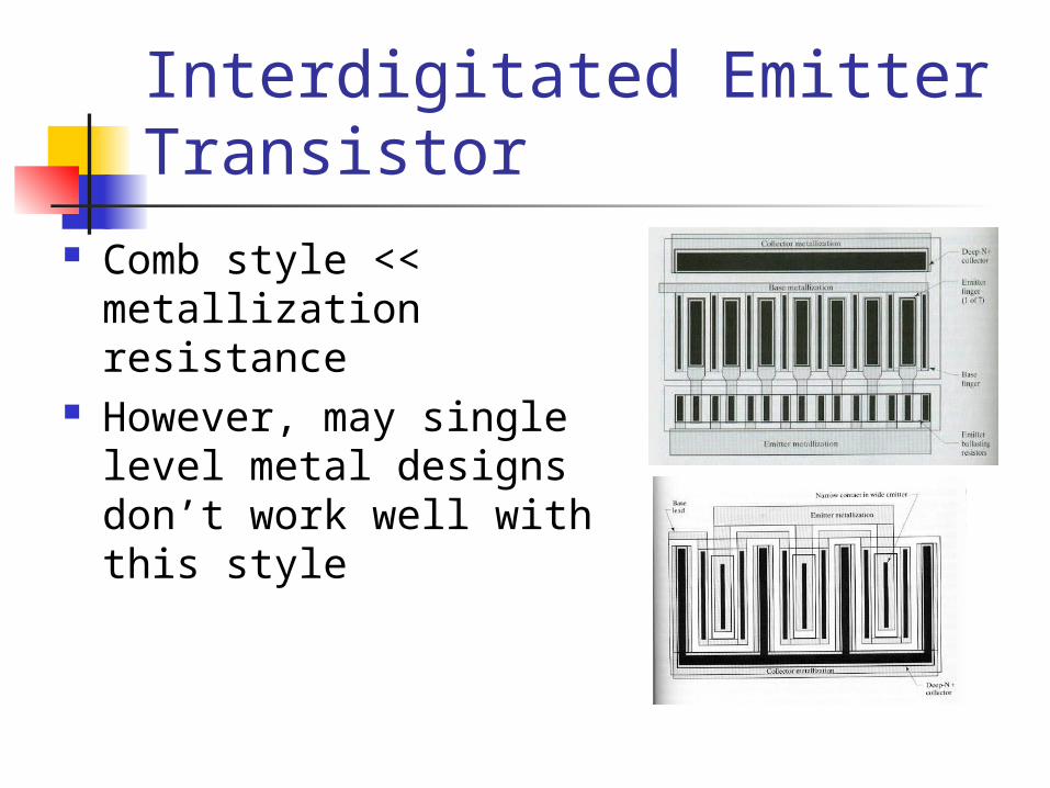
Comb style << metallization resistance
However, may single level metal designs don’t work well with this style
Interdigitated Emitter Transistor
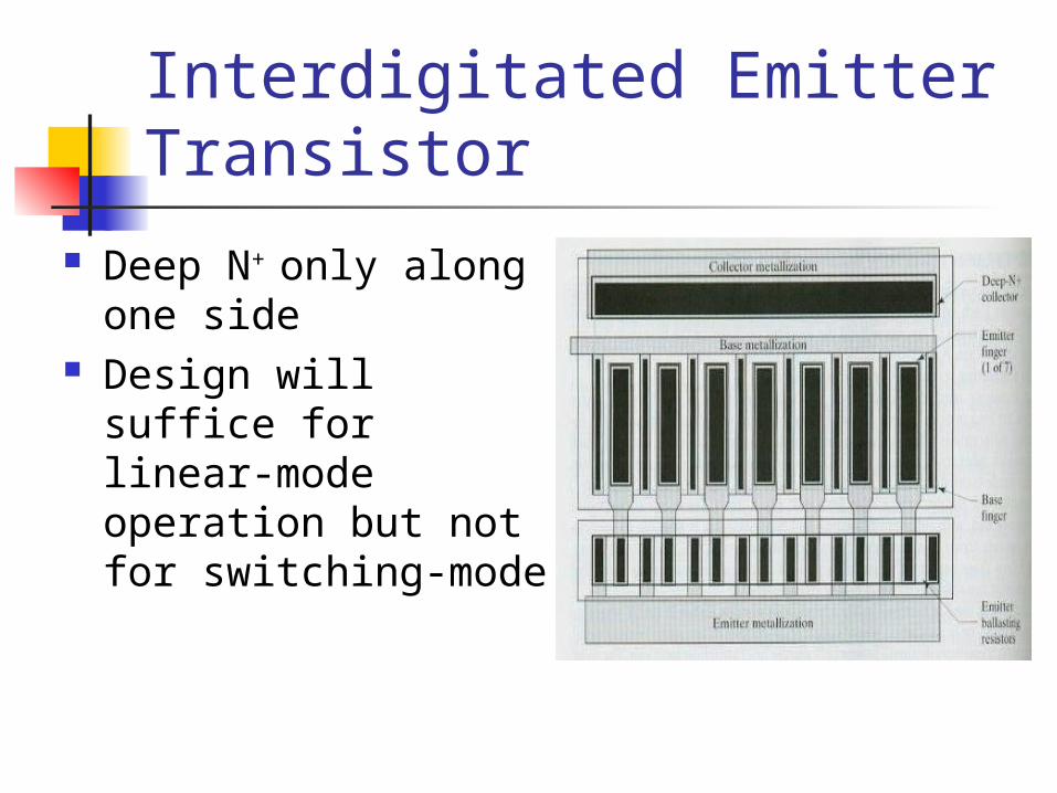
Deep N+ only along one side
Design will suffice for linear-mode operation but not for switching-mode
Interdigitated Emitter Transistor
For switching-mode at high currents RC= RVN+ + RLNBL
To reduce RVN+ increase deep N+ area
To reduce RLNBL contact NBL along a longer
periphery or decrease distance between active regions and sinkers
Other options include: placing sinkers along both sides and unbroken ring of N+
Interdigitated Emitter Transistor
Can operate at higher speeds due to low base resistance
Narrow emitter fingers Reduce base resistance
Control emitter crowding However, narrow emitters prone to
intrafinger debiasing Use of ballasting resistors can help
normalize current flow in each finger, but cannot prevent intrafinger debiasing
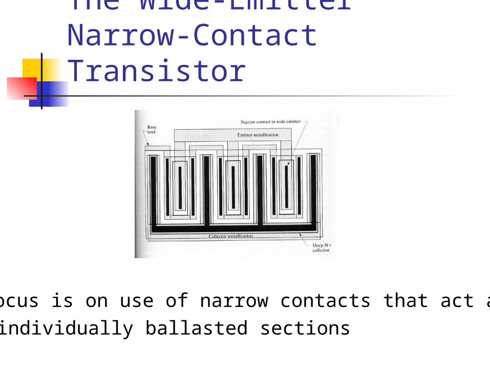
The Wide-Emitter Narrow-Contact Transistor
Focus is on use of narrow contacts that act as individually ballasted sections
The Wide-Emitter Narrow-Contact Transistor
Idea Behind Design Each finger is divided into individually
ballasted sections No one portion of the emitter can conduct
more current than any other Not feasible to segment fingers
Narrow emitter contact on a wide finger provides similar benefit
The Wide-Emitter Narrow-Contact Transistor
Wide-emitter finger with narrow contact =Distributed network of ballasting resistors
Network is made up of Emitter resistance Pinched base resistance
Emitter resistence Largest at periphery Smallest at center
Base resistance Smallest at periphery
Largest at center
The Wide-Emitter Narrow-Contact Transistor
The network of emitter and base resistors complement each other
At low currents RB is small Uniform current flow
As currents increase Debiasing causes the currents to move out to
the periphery RE has increased due to increased currents
Emitter voltage drops counter act conduction gradients due to debiasing
Therefore, RE and RB ensure uniform current flow
The Wide-Emitter Narrow-Contact Transistor
Specifics Sufficient emitter overlap of contact Typical emitter overlaps of 12 to 25 um Larger overlaps slow frequency
response Smaller overlaps don’t provide enough
ballasting to prevent failure mechanisms
The Wide-Emitter Narrow-Contact Transistor
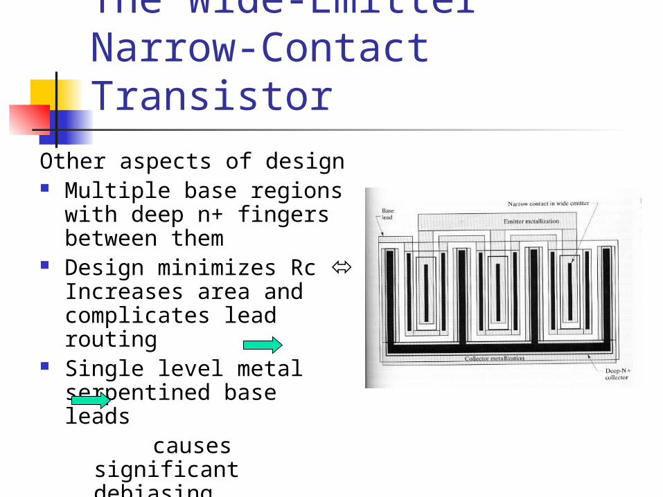
Other aspects of design Multiple base regions with
deep n+ fingers between them
Design minimizes Rc Increases area and complicates lead routing
Single level metal serpentined base leads causes significant
debiasing
The Wide-Emitter Narrow-Contact Transistor
Overview Very robust Distributed ballasting helps prevent failure
mechanisms allowing for increased current densities
Under harsh conditions ballasting resistors inserted into leads will help
Design does not switch as fast previous design
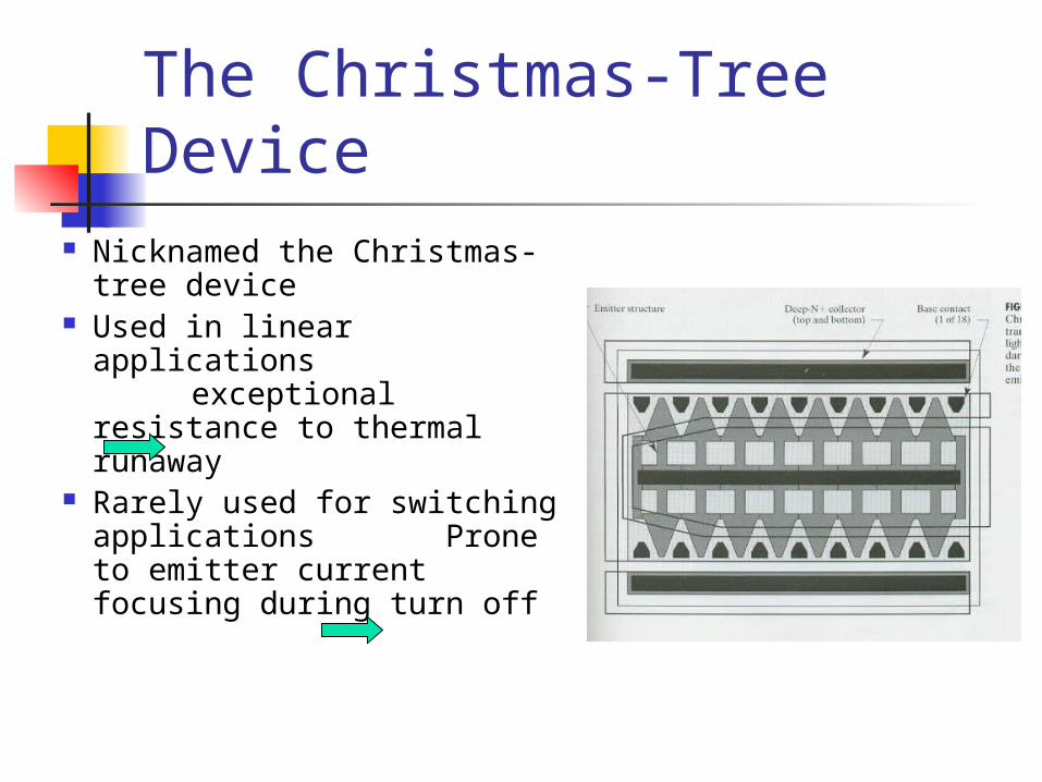
The Christmas-Tree Device Nicknamed the
Christmas-tree device Used in linear
applications exceptional resistance to thermal runaway
Rarely used for switching applications Prone to emitter current focusing during turn off
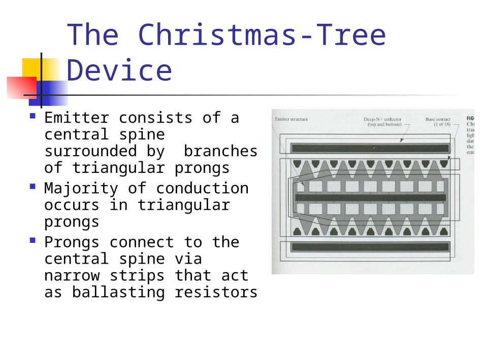
The Christmas-Tree Device Emitter consists of a
central spine surrounded by branches of triangular prongs
Majority of conduction occurs in triangular prongs
Prongs connect to the central spine via narrow strips that act as ballasting resistors
The Christmas-Tree Device Current increases emitter crowding conduction moves to periphery current flows
through ballasting resistor This distributed ballasting increases resistance to
thermal runaway Due to wide emitter layout is vulnerable to emitter
currently focusing At turn off condition moves from periphery
toward spine concentration of increased current leads to secondary breakdown
The Christmas-Tree Device This device is best in applications that dissipate
large amounts of power without abrupt turn off transitions
Wide-emitter narrow-contact structure exhibits superior immunity to secondary breakdown because of decreased width
Device chosen for: series-pass devices of linear voltage regulators Output stages of audio power amplifiers
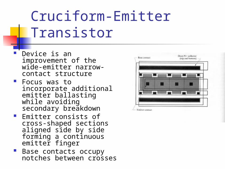
Cruciform-Emitter Transistor
Device is an improvement of the wide-emitter narrow-contact structure
Focus was to incorporate additional emitter ballasting while avoiding secondary breakdown
Emitter consists of cross-shaped sections aligned side by side forming a continuous emitter finger
Base contacts occupy notches between crosses
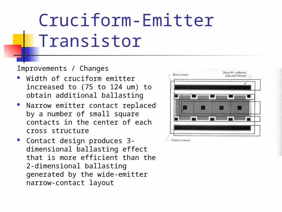
Cruciform-Emitter Transistor
Improvements / Changes Width of cruciform emitter increased
to (75 to 124 um) to obtain additional ballasting
Narrow emitter contact replaced by a number of small square contacts in the center of each cross structure
Contact design produces 3-dimensional ballasting effect that is more efficient than the 2-dimensional ballasting generated by the wide-emitter narrow-contact layout
Cruciform-Emitter Transistor
Overview Cruciform design combines best features of
Christmas-tree and WENC Contact to emitter ratio of WENC design Resistance to thermal runaway due to increased
ballasting exploited by Christmas-tree design Out performs the Christmas-tree device with
respect to secondary breakdown Extremely efficient use of space
Cruciform-Emitter Transistor
Overview Two drawbacks associated with this
design First, small emitter contacts high
localized current densities in metallization vulnerable to electromigration
This effect can reduced by replacing small contacts with array of minimum contacts to increase sidewall perimeter
Cruciform-Emitter Transistor Second, compact design can cause
extreme localized heating at high power levels
Less area – efficient transistor are preferred to compact designs
This structure is therefore best suited for switching applications because these applications are constrained more by current handling capabilities than by power dissipation

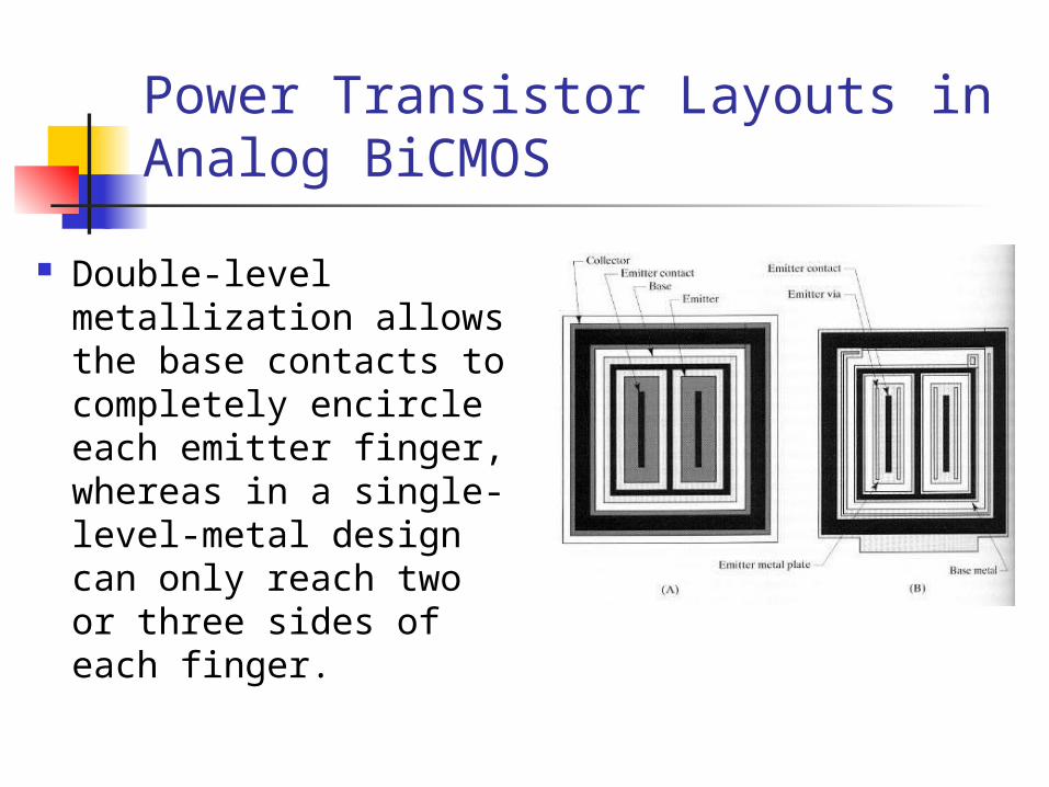
Power Transistor Layouts in Analog BiCMOS
Double-level metallization allows the base contacts to completely encircle each emitter finger, whereas in a single-level-metal design can only reach two or three sides of each finger.
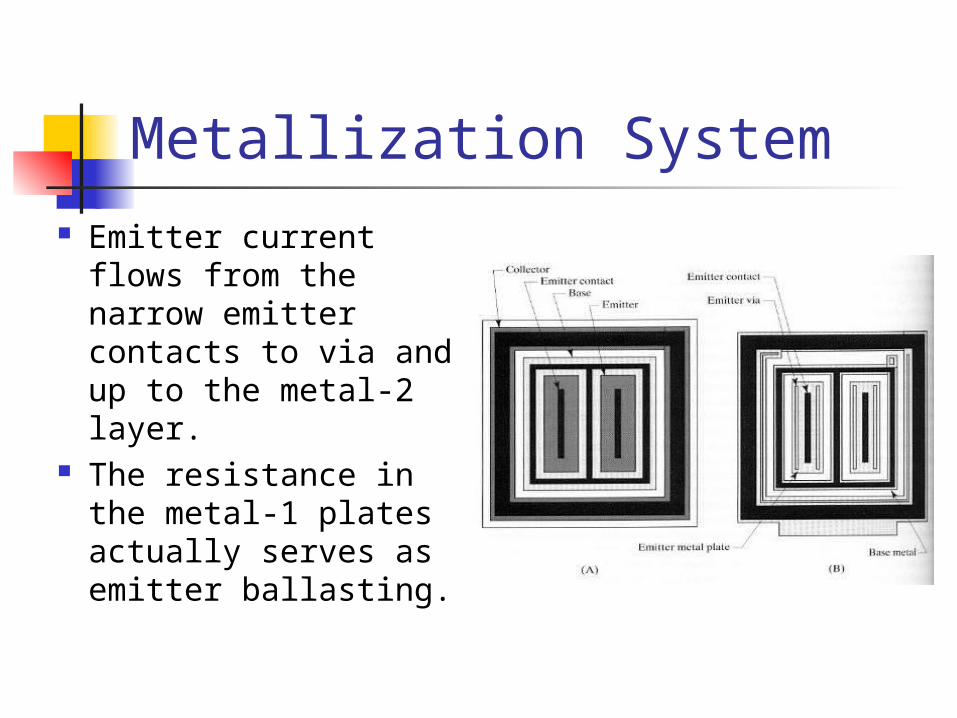
Metallization System Emitter current
flows from the narrow emitter contacts to via and up to the metal-2 layer.
The resistance in the metal-1 plates actually serves as emitter ballasting.
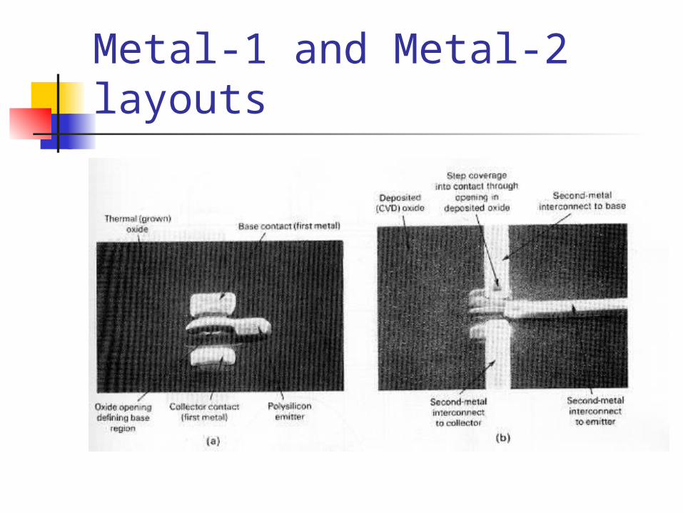
Metal-1 and Metal-2 layouts
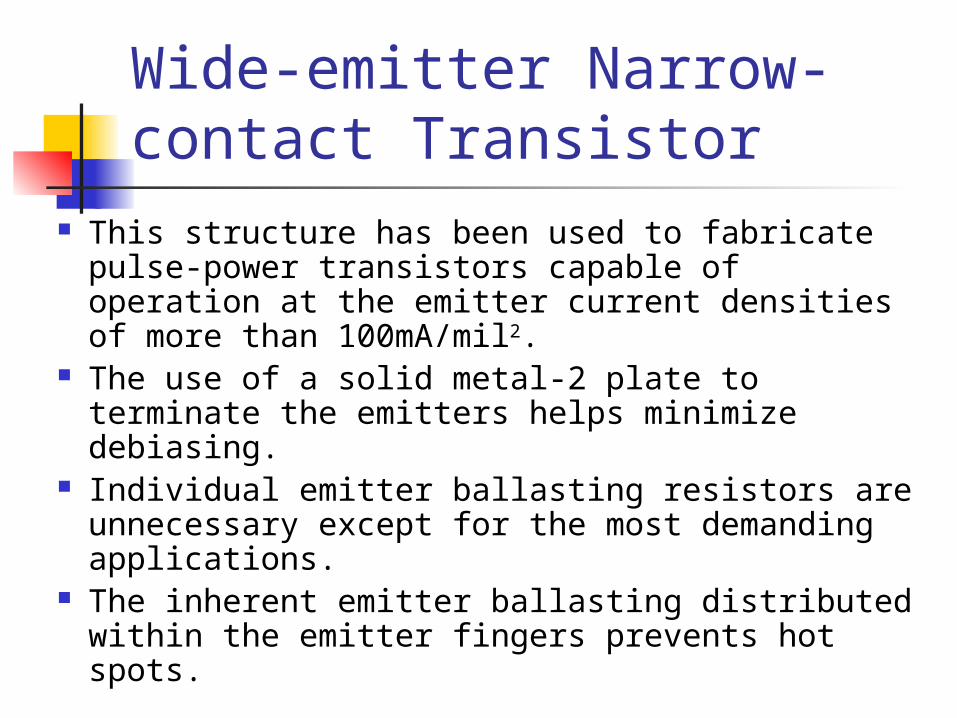
Wide-emitter Narrow-contact Transistor
This structure has been used to fabricate pulse-power transistors capable of operation at the emitter current densities of more than 100mA/mil2.
The use of a solid metal-2 plate to terminate the emitters helps minimize debiasing.
Individual emitter ballasting resistors are unnecessary except for the most demanding applications.
The inherent emitter ballasting distributed within the emitter fingers prevents hot spots.
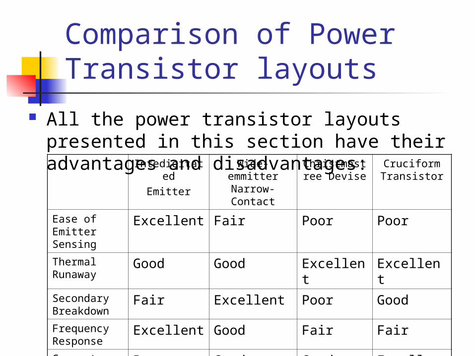
Comparison of Power Transistor layouts
All the power transistor layouts presented in this section have their advantages and disadvantages:Intedigitated
EmitterWide-
emmitter Narrow-Contact
Christmastree Devise
Cruciform Transistor
Ease of Emitter Sensing
Excellent Fair Poor Poor
Thermal Runaway
Good Good Excellent Excellent
Secondary Breakdown
Fair Excellent Poor Good
Frequency Response
Excellent Good Fair Fair
Compactness of Layout
Poor Good Good Excellent

Saturation Detection and Limiting
Substrate injection Effects:
Waste supply current Substrate debiasing Device latchup
Preventing measures: Inspecting minority carriers Preventing the transistor from saturation

Substrate Injection
Emitter of lateral NPN injects minority carriers into tank
Small signal transformers inject minimal amounts of current
Large lateral PNP produces currents of 10-100 mA
Debasing occurs triggering latchup

Prevent Minority Carriers
Unbroken ring of deep-N+ around outside edge of tank
Ring merges with NBL and completely encloses the base
Minority carriers recombine before reaching isolation
Compatible with BiCMOS and less effective in CDI processes
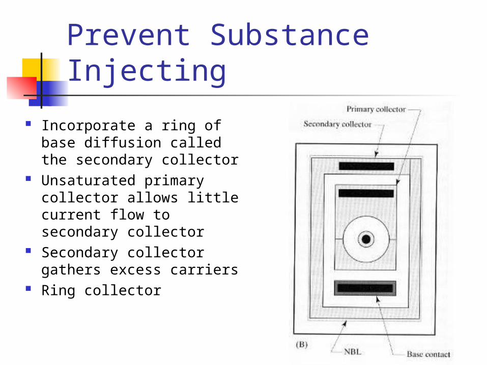
Prevent Substance Injecting
Incorporate a ring of base diffusion called the secondary collector
Unsaturated primary collector allows little current flow to secondary collector
Secondary collector gathers excess carriers
Ring collector

The Secondary Collector 1/2
Secondary collector connected to ground Returns carriers to ground line At saturation emitter current flows to ground Functions as an unprotected lateral transistor
without substrate debiasing Secondary collector connected to base lead
At saturation apparent beta rapidly declines Functions as a deep-N+ guardring Increase efficiency with guardring combination

The Secondary Collector 2/2
Analog BiCMOS processes Base diffusion instead of P-type Source Drain Less effective than standard bipolar
processes Functions as a Saturation Detector
Current flowing in secondary collector No need to encircle entire transistor Dynamic antisaturation circuit
Deep-N+ ring suppress transient substrate injection
Saturating NPN Transistor Inject current into the substance Protection against minority carriers injection
Greater than few milliamps of base drive Deep-N+ ring surrounding periphery of the
collector Contains minority carriers inside the tank Reduces collector resistance
Base diffusion used in saturation detection Power switching transistors incorporate
small base diffusion
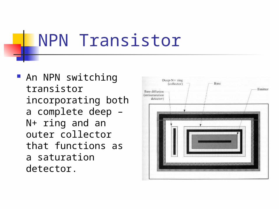
NPN Transistor
An NPN switching transistor incorporating both a complete deep –N+ ring and an outer collector that functions as a saturation detector.
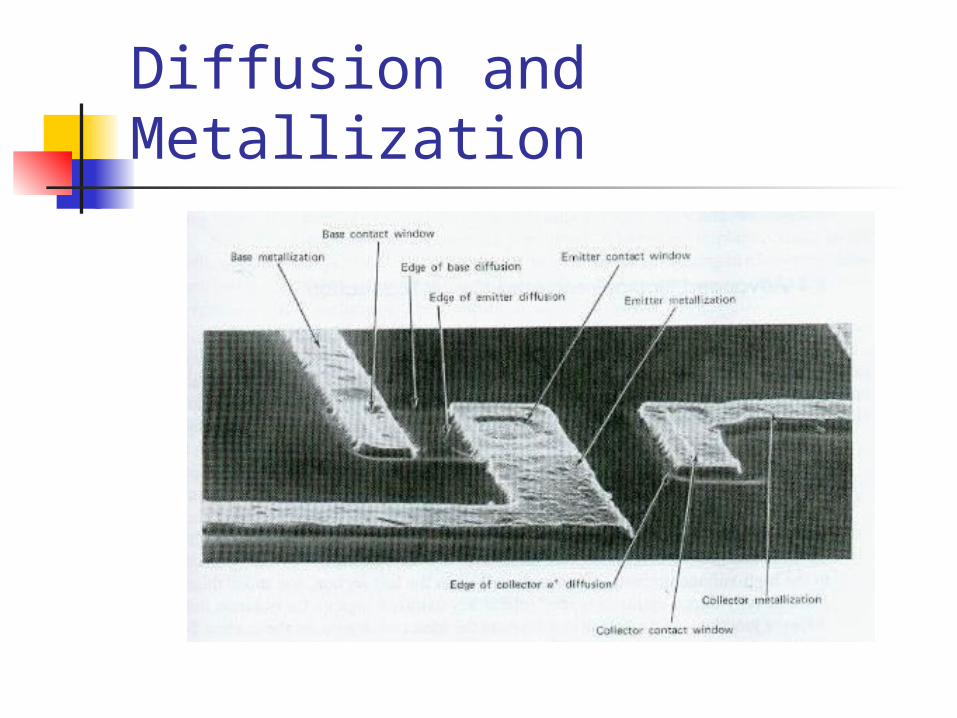
Diffusion and Metallization
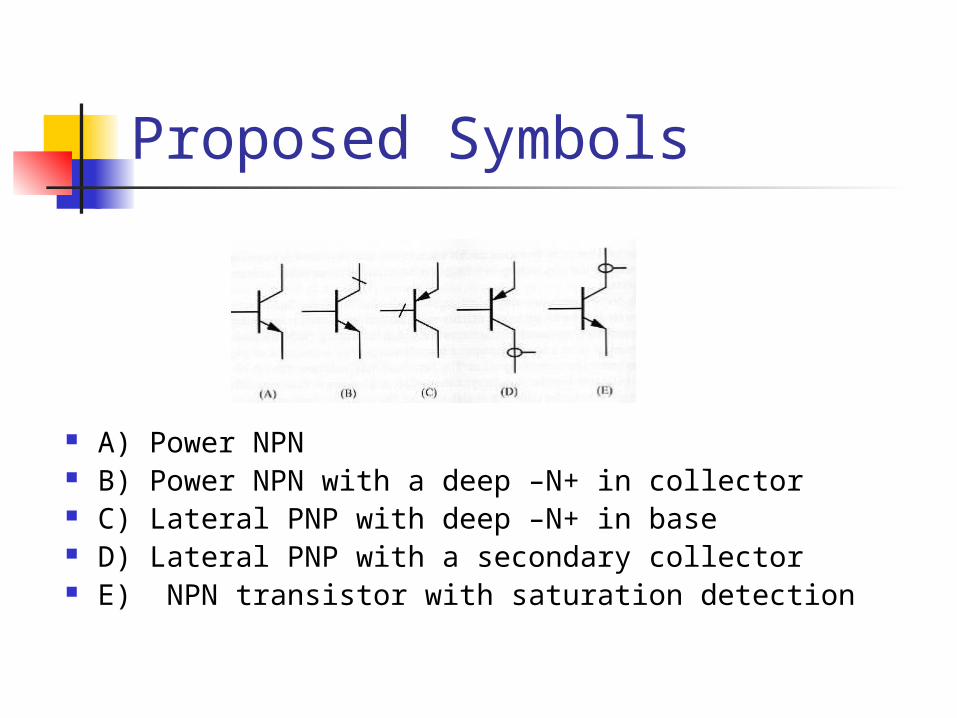
Proposed Symbols
A) Power NPN B) Power NPN with a deep –N+ in collector C) Lateral PNP with deep –N+ in base D) Lateral PNP with a secondary collector E) NPN transistor with saturation detection
References
The Art of Analog Layout, by Roy Alan Hastings, Prentice Hall, Upper Saddle River, NJ, ©2000.
Analysis and Design of Analog Integrated Circuits, 4th ed., by Gray, Hurst, Lewis and Meyer, Wiley, New York, ©2001.
Recommended