Road to Chiplets: ArchitectureJuly 13 & 14, 2021
www.meptec.org
Pathfinding and Design of Large-Scale Chiplet-Based Systems
PUNEET GUPTA ([email protected])
UNIVERSITY OF CALIFORNIA, LOS ANGELES
PUNEET GUPTA (HTTPS://NANOCAD.EE.UCLA.EDU) 1
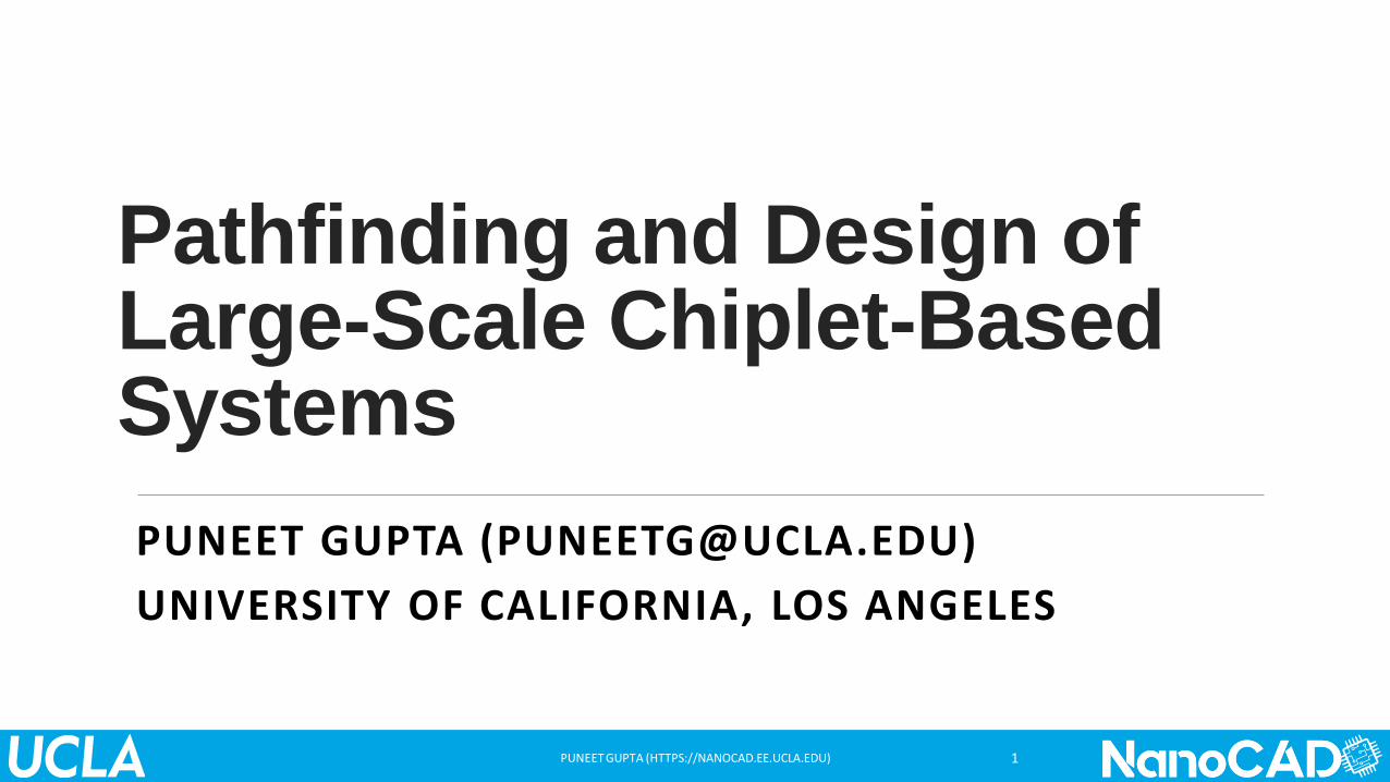
How much can you gain by the Chiplet approach?
Up to 2.1X gain by system customization!
◦ Hypothetical study based on processor + cache chiplets and application specific customization
PUNEET GUPTA (HTTPS://NANOCAD.EE.UCLA.EDU) 2
SPEC2006 EEMBC SPLASH-2 NPB
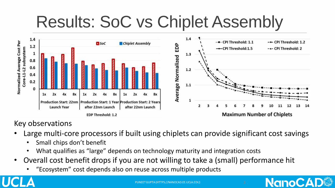
Results: SoC vs Chiplet Assembly
PUNEET GUPTA (HTTPS://NANOCAD.EE.UCLA.EDU) 3
Key observations• Large multi-core processors if built using chiplets can provide significant cost savings
• Small chips don’t benefit• What qualifies as “large” depends on technology maturity and integration costs
• Overall cost benefit drops if you are not willing to take a (small) performance hit• “Ecosystem” cost depends also on reuse across multiple products
Designing Large Chiplet-based SystemsTO APPEAR IN DAC ’21
PUNEET GUPTA (HTTPS://NANOCAD.EE.UCLA.EDU) 4
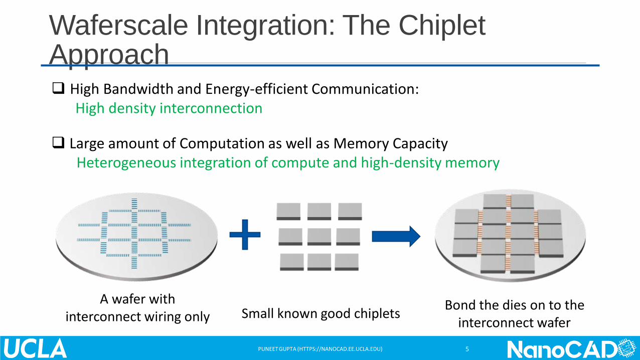
Waferscale Integration: The ChipletApproach
PUNEET GUPTA (HTTPS://NANOCAD.EE.UCLA.EDU) 5
Bond the dies on to the interconnect wafer
Small known good chipletsA wafer with
interconnect wiring only
❑ High Bandwidth and Energy-efficient Communication:High density interconnection
❑ Large amount of Computation as well as Memory CapacityHeterogeneous integration of compute and high-density memory
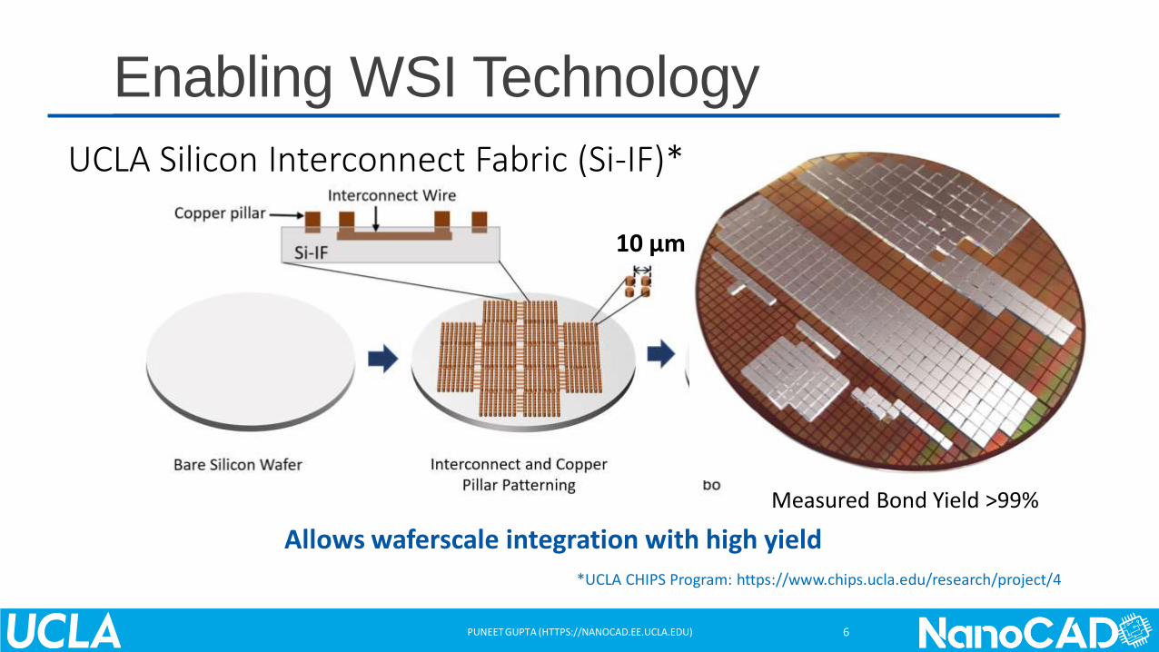
Enabling WSI Technology
PUNEET GUPTA (HTTPS://NANOCAD.EE.UCLA.EDU) 6
UCLA Silicon Interconnect Fabric (Si-IF)*
2 µm10 µm
100 µm
*UCLA CHIPS Program: https://www.chips.ucla.edu/research/project/4
Allows waferscale integration with high yield
Measured Bond Yield >99%
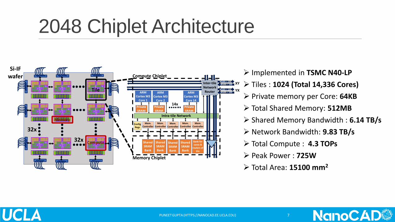
32x
32x
Tile
Compute
Memory
Si-IF wafer
XY
YXARM
Cortex M3 Core 1
Private SRAM
Intra-tile Network
Inter-tile NetworkRouter
Width = 100
Width = 100
Width = 100
Width = 100
Config Regs
Mem. Controller
Shared SRAM Bank
Mem. Controller
Shared SRAM Bank
Mem. Controller
Shared SRAM Bank
Mem. Controller
Shared SRAM Bank
Mem. Controller
Bank for cores &
routers of tile
ARM Cortex M3
Core 14
Private SRAM
ARM Cortex M3
Core 2
Private SRAM
Compute Chiplet
Memory Chiplet
14x
➢ Implemented in TSMC N40-LP
➢ Tiles : 1024 (Total 14,336 Cores)
➢ Private memory per Core: 64KB
➢ Total Shared Memory: 512MB
➢ Shared Memory Bandwidth : 6.14 TB/s
➢ Network Bandwidth: 9.83 TB/s
➢ Total Compute : 4.3 TOPs
➢ Peak Power : 725W
➢ Total Area: 15100 mm2
7
2048 Chiplet Architecture
PUNEET GUPTA (HTTPS://NANOCAD.EE.UCLA.EDU)
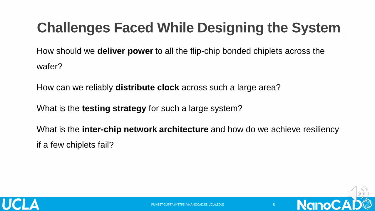
Challenges Faced While Designing the System
How should we deliver power to all the flip-chip bonded chiplets across the
wafer?
How can we reliably distribute clock across such a large area?
What is the testing strategy for such a large system?
What is the inter-chip network architecture and how do we achieve resiliency
if a few chiplets fail?
8PUNEET GUPTA (HTTPS://NANOCAD.EE.UCLA.EDU)
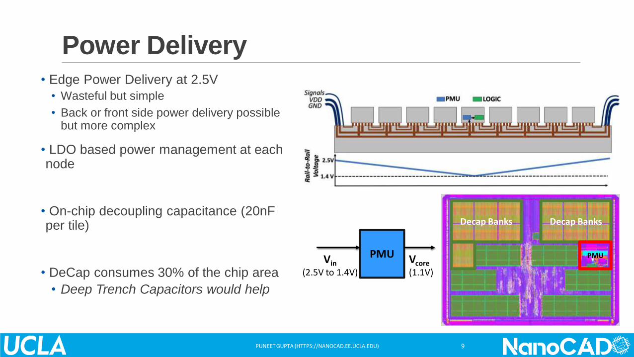
Power Delivery• Edge Power Delivery at 2.5V
• Wasteful but simple
• Back or front side power delivery possible but more complex
• LDO based power management at each node
• On-chip decoupling capacitance (20nF per tile)
• DeCap consumes 30% of the chip area
• Deep Trench Capacitors would help
9
Decap Banks Decap Banks
PMUPMUVin(2.5V to 1.4V)
Vcore(1.1V)
PUNEET GUPTA (HTTPS://NANOCAD.EE.UCLA.EDU)
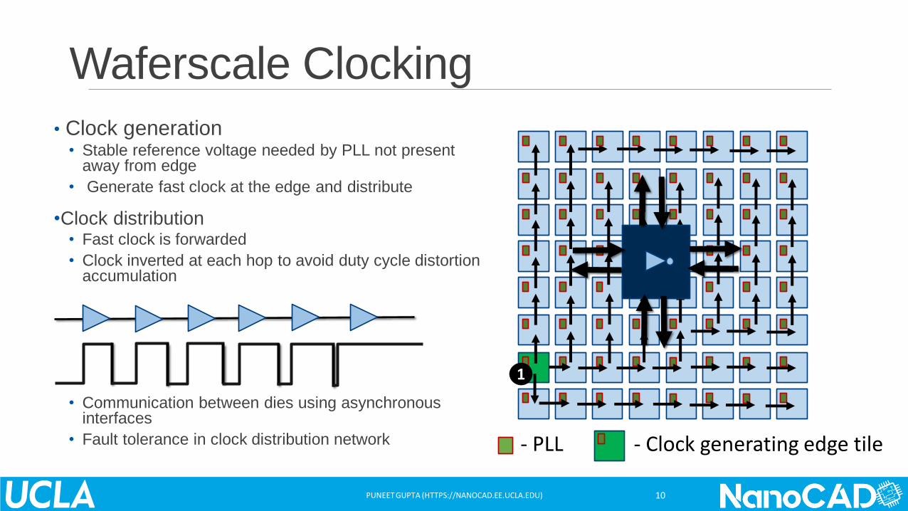
Waferscale Clocking
• Clock generation• Stable reference voltage needed by PLL not present
away from edge
• Generate fast clock at the edge and distribute
•Clock distribution• Fast clock is forwarded
• Clock inverted at each hop to avoid duty cycle distortion accumulation
• Communication between dies using asynchronous interfaces
• Fault tolerance in clock distribution network
PUNEET GUPTA (HTTPS://NANOCAD.EE.UCLA.EDU) 10
1
- PLL - Clock generating edge tile
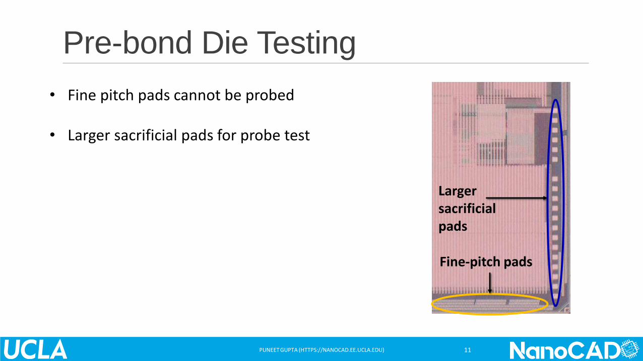
Pre-bond Die Testing
PUNEET GUPTA (HTTPS://NANOCAD.EE.UCLA.EDU) 11
• Fine pitch pads cannot be probed
• Larger sacrificial pads for probe test
Larger sacrificial pads
Fine-pitch pads
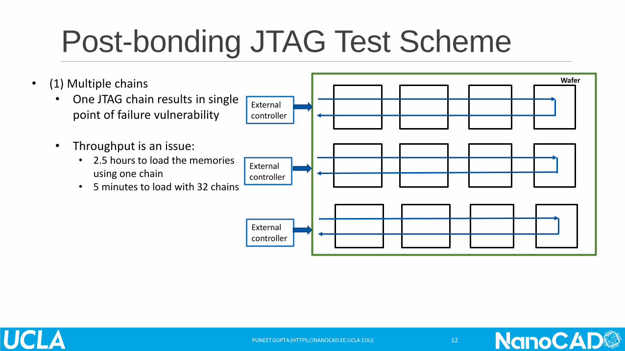
Post-bonding JTAG Test Scheme
PUNEET GUPTA (HTTPS://NANOCAD.EE.UCLA.EDU) 12
External controller
External controller
External controller
Wafer• (1) Multiple chains• One JTAG chain results in single
point of failure vulnerability
• Throughput is an issue:• 2.5 hours to load the memories
using one chain• 5 minutes to load with 32 chains
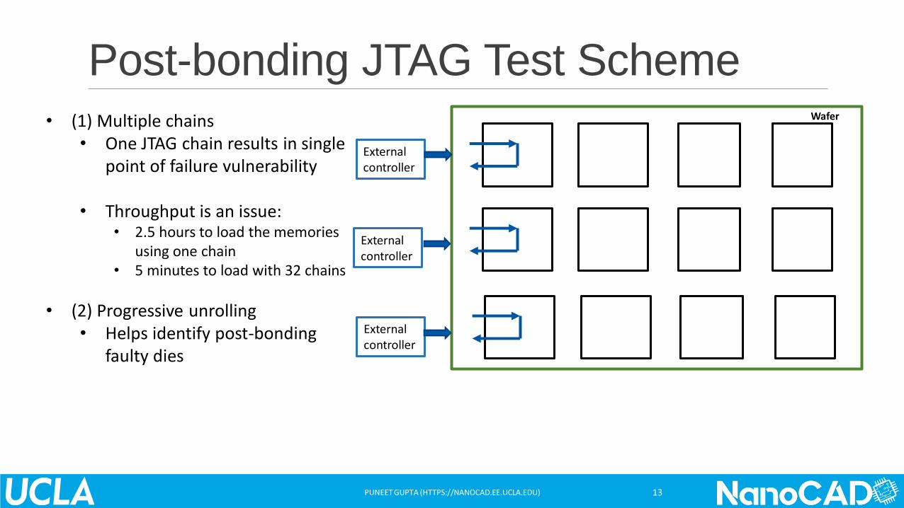
Post-bonding JTAG Test Scheme
PUNEET GUPTA (HTTPS://NANOCAD.EE.UCLA.EDU) 13
External controller
External controller
External controller
Wafer• (1) Multiple chains• One JTAG chain results in single
point of failure vulnerability
• Throughput is an issue:• 2.5 hours to load the memories
using one chain• 5 minutes to load with 32 chains
• (2) Progressive unrolling• Helps identify post-bonding
faulty dies
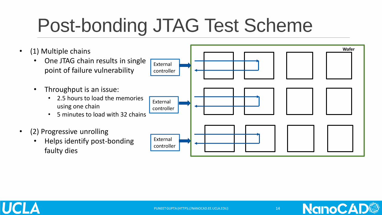
Post-bonding JTAG Test Scheme
PUNEET GUPTA (HTTPS://NANOCAD.EE.UCLA.EDU) 14
External controller
External controller
External controller
Wafer• (1) Multiple chains• One JTAG chain results in single
point of failure vulnerability
• Throughput is an issue:• 2.5 hours to load the memories
using one chain• 5 minutes to load with 32 chains
• (2) Progressive unrolling• Helps identify post-bonding
faulty dies
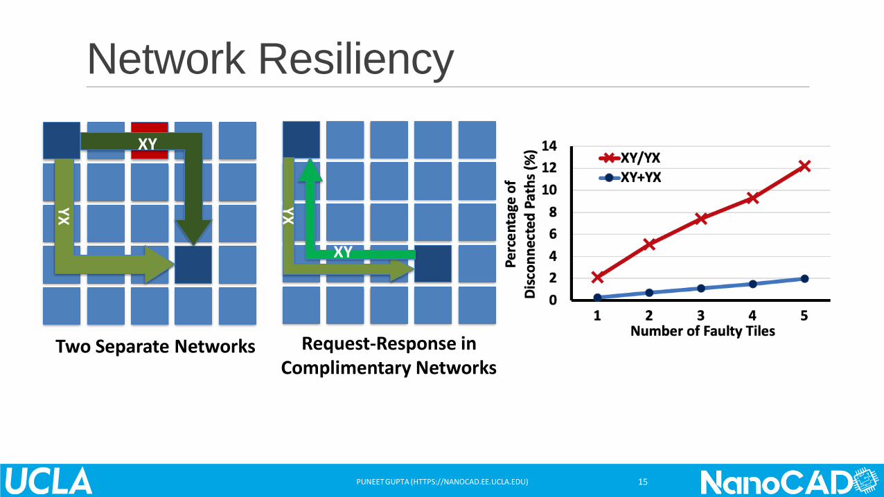
Network Resiliency
PUNEET GUPTA (HTTPS://NANOCAD.EE.UCLA.EDU) 15
YX
XY
YX
XY
Two Separate Networks Request-Response in Complimentary Networks
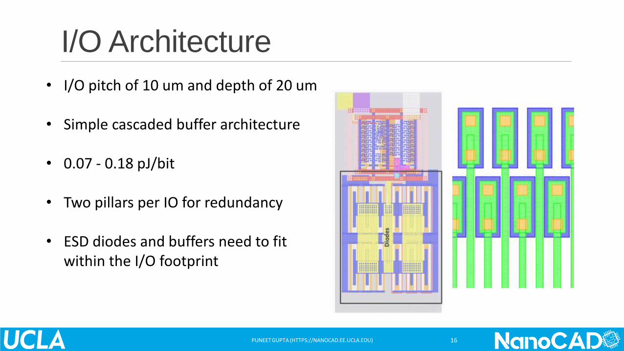
I/O Architecture
PUNEET GUPTA (HTTPS://NANOCAD.EE.UCLA.EDU) 16
• I/O pitch of 10 um and depth of 20 um
• Simple cascaded buffer architecture
• 0.07 - 0.18 pJ/bit
• Two pillars per IO for redundancy
• ESD diodes and buffers need to fit within the I/O footprint
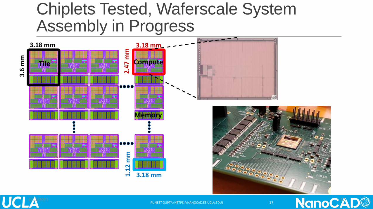
Chiplets Tested, Waferscale System Assembly in Progress
PUNEET GUPTA (HTTPS://NANOCAD.EE.UCLA.EDU) 177/11/2021 17
Tile Compute
Memory
3.18 mm
2.4
7 m
m
3.18 mm1.1
2 m
m
3.18 mm
3.6
mm
Pathfinding 2.5D SubstratesAPPEARED IN SLIP ’20
PUNEET GUPTA (HTTPS://NANOCAD.EE.UCLA.EDU) 18
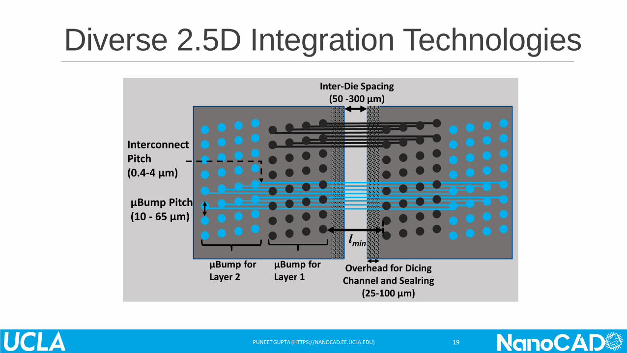
Diverse 2.5D Integration Technologies
PUNEET GUPTA (HTTPS://NANOCAD.EE.UCLA.EDU) 19
µBump forLayer 1
Inter-Die Spacing (50 -300 µm)
µBump forLayer 2
Overhead for Dicing Channel and Sealring
(25-100 µm)
µBump Pitch(10 - 65 µm)
InterconnectPitch(0.4-4 µm)
lmin
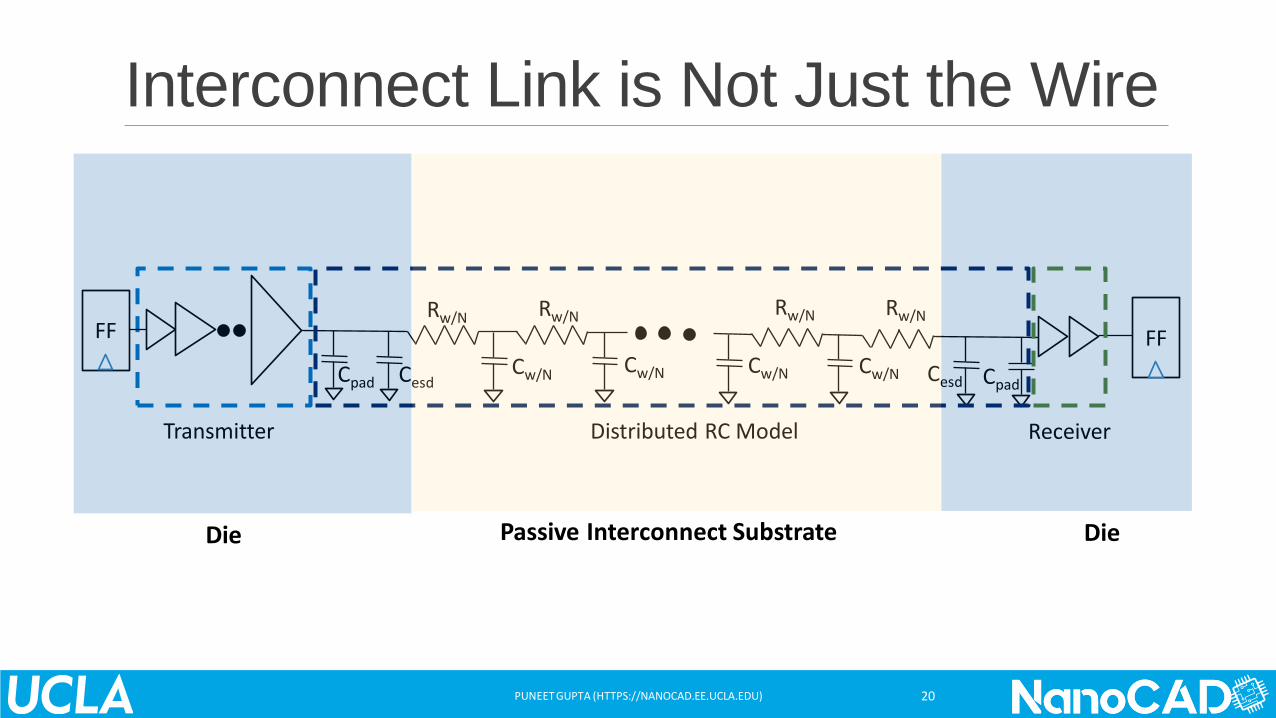
Interconnect Link is Not Just the Wire
PUNEET GUPTA (HTTPS://NANOCAD.EE.UCLA.EDU) 20
Transmitter
Cpad CesdCw/N Cw/N
Rw/NRw/N
Cw/N
Rw/N
Cw/N
Rw/N
Cesd Cpad
ReceiverDistributed RC Model
FFFF
Die DiePassive Interconnect Substrate
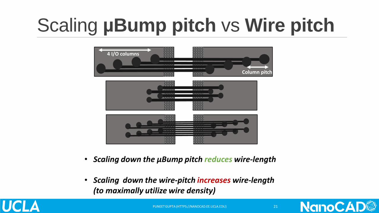
Scaling µBump pitch vs Wire pitch
PUNEET GUPTA (HTTPS://NANOCAD.EE.UCLA.EDU) 21
• Scaling down the µBump pitch reduces wire-length
• Scaling down the wire-pitch increases wire-length (to maximally utilize wire density)
4 I/O columns
Column pitch
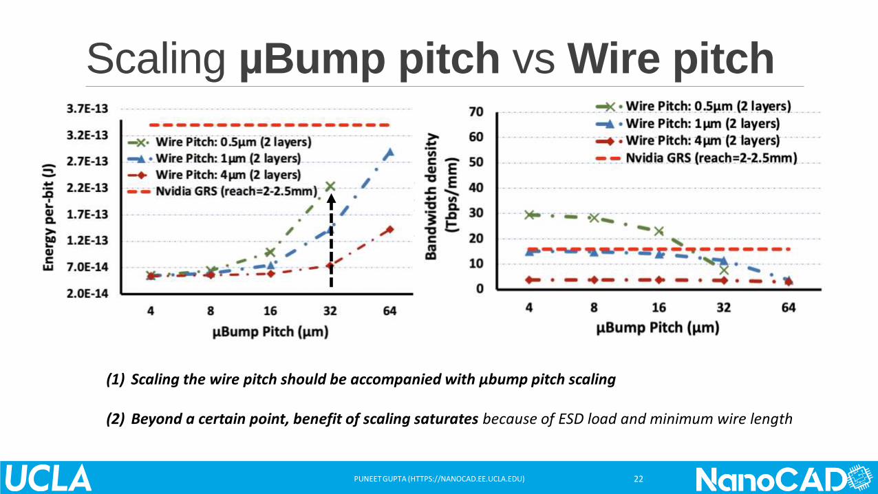
Scaling µBump pitch vs Wire pitch
PUNEET GUPTA (HTTPS://NANOCAD.EE.UCLA.EDU) 22
(1) Scaling the wire pitch should be accompanied with µbump pitch scaling
(2) Beyond a certain point, benefit of scaling saturates because of ESD load and minimum wire length
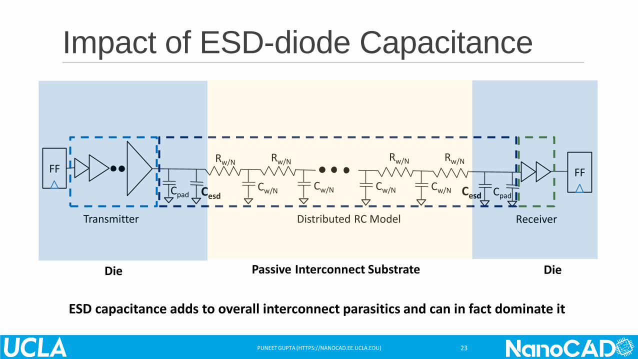
Impact of ESD-diode Capacitance
PUNEET GUPTA (HTTPS://NANOCAD.EE.UCLA.EDU) 23
Transmitter
Cpad CesdCw/N Cw/N
Rw/NRw/N
Cw/N
Rw/N
Cw/N
Rw/N
Cesd Cpad
ReceiverDistributed RC Model
FFFF
Die DiePassive Interconnect Substrate
ESD capacitance adds to overall interconnect parasitics and can in fact dominate it
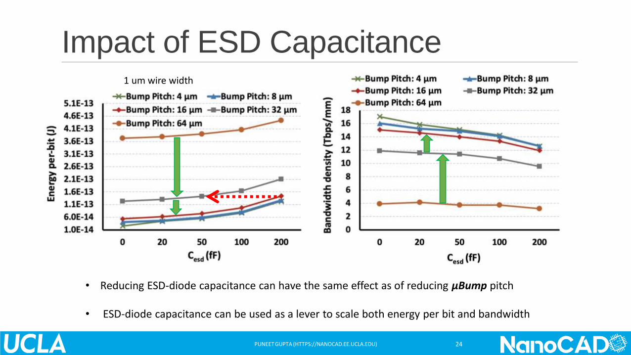
Impact of ESD Capacitance
PUNEET GUPTA (HTTPS://NANOCAD.EE.UCLA.EDU) 24
• Reducing ESD-diode capacitance can have the same effect as of reducing µBump pitch
• ESD-diode capacitance can be used as a lever to scale both energy per bit and bandwidth
1 um wire width
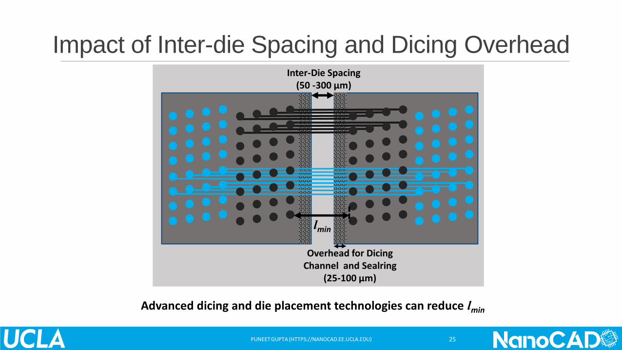
Impact of Inter-die Spacing and Dicing Overhead
PUNEET GUPTA (HTTPS://NANOCAD.EE.UCLA.EDU) 25
Inter-Die Spacing (50 -300 µm)
Overhead for Dicing Channel and Sealring
(25-100 µm)
lmin
Advanced dicing and die placement technologies can reduce lmin
Impact of Inter-die Spacing and Dicing Overhead
PUNEET GUPTA (HTTPS://NANOCAD.EE.UCLA.EDU) 26
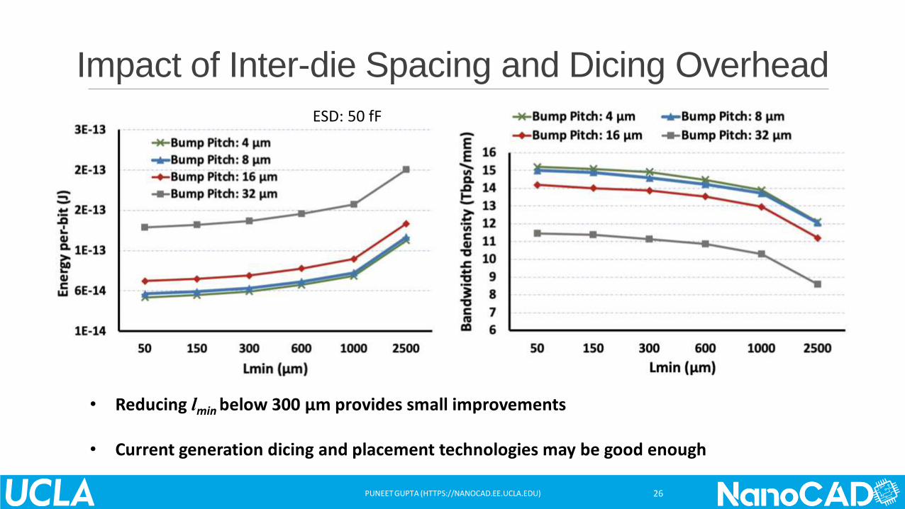
• Reducing lmin below 300 µm provides small improvements
• Current generation dicing and placement technologies may be good enough
ESD: 50 fF
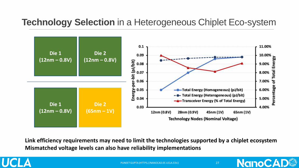
Technology Selection in a Heterogeneous Chiplet Eco-system
PUNEET GUPTA (HTTPS://NANOCAD.EE.UCLA.EDU) 27
Die 1(12nm – 0.8V)
Die 2(12nm – 0.8V)
Die 1(12nm – 0.8V)
Die 2(65nm – 1V)
Link efficiency requirements may need to limit the technologies supported by a chiplet ecosystemMismatched voltage levels can also have reliability implementations
ConclusionsChiplets offer THREE primary advantages at the system-level
1. Heterogeneity.◦ Integrate logic non-compatible memories + network interfaces
◦ Selective upgrades to system IPs
2. Scale◦ Ability to build large systems without yield concerns
◦ Possibility to go beyond reticle size boundaries (e.g., waferscale)
3. (Lower-cost) Customization◦ May be we will see chiplet system variety comparable to board-level systems in near future…
But
• Cost benefits are suspect for high volume, moderately sized SoCs
• Ecosystem challenges remain
• “Wildly” heterogeneous chiplet systems may not be a good idea
PUNEET GUPTA (HTTPS://NANOCAD.EE.UCLA.EDU) 28
Backup
PUNEET GUPTA (HTTPS://NANOCAD.EE.UCLA.EDU) 29

Thank you sponsors!

Advantest receives highest ratings from customers in
annual VLSIresearch Customer Satisfaction Survey
for 2 consecutive years.
“Year-after-year the company has delivered on its promise
of technological excellence and it remains clear that Advantest
keeps their customers’ successes central to their strategy.
Congratulations on celebrating 33 years of recognition
for outstanding customer satisfaction.”
— Risto Puhakka, President VLSIresearch
Global customers name Advantest THE BEST
supplier of test equipment in 2020 and 2021,
with highest ratings in categories of:
Technical Leadership – Partnership – Trust
– Recommended Supplier – Field Service
Global Companies Rate Advantest THE BEST ATE Company 2021
COPYRIGHT NOTICE
This presentation in this publication was presented at the Road to Chiplets: Architecture Workshop(July 13 & 14, 2021). The content reflects the opinion of the author(s) and their respective companies. The inclusion of presentations in this publication does not constitute an endorsement by MEPTEC or the sponsors.
There is no copyright protection claimed by this publication. However, each presentation is the work of the authors and their respective companies and may contain copyrighted material. As such, it is strongly encouraged that any use reflect proper acknowledgement to the appropriate source. Any questions regarding the use of any materials presented should be directed to the author(s) or their companies.
www.meptec.org
Recommended