Quasi-particle electronic band structure and alignment of the V-VI-VII semiconductorsSbSI, SbSBr, and SbSeI for solar cellsKeith T. Butler, Scott McKechnie, Pooya Azarhoosh, Mark van Schilfgaarde, David O. Scanlon, and Aron Walsh Citation: Applied Physics Letters 108, 112103 (2016); doi: 10.1063/1.4943973 View online: http://dx.doi.org/10.1063/1.4943973 View Table of Contents: http://scitation.aip.org/content/aip/journal/apl/108/11?ver=pdfcov Published by the AIP Publishing Articles you may be interested in First-principles study on electronic and optical properties of Cu2ZnSiV I4 (VI=S, Se, and Te) quaternarysemiconductors AIP Advances 5, 057111 (2015); 10.1063/1.4920936 Band alignment at Sb 2 S 3 / Cu ( In , Ga ) Se 2 heterojunctions and electronic characteristics of solar celldevices based on them Appl. Phys. Lett. 96, 262101 (2010); 10.1063/1.3457439 Large‐band‐gap SiC, III‐V nitride, and II‐VI ZnSe‐based semiconductor device technologies J. Appl. Phys. 76, 1363 (1994); 10.1063/1.358463 I–III–VI2 compound semiconductors for solar cell applications J. Vac. Sci. Technol. A 10, 2006 (1992); 10.1116/1.578017 NEW FERROELECTRIC V. VI. VII COMPOUNDS OF THE SbSI TYPE Appl. Phys. Lett. 4, 210 (1964); 10.1063/1.1753944
Reuse of AIP Publishing content is subject to the terms at: https://publishing.aip.org/authors/rights-and-permissions. Download to IP: 138.38.25.29 On: Tue, 15 Mar 2016
15:20:42

Quasi-particle electronic band structure and alignment of the V-VI-VIIsemiconductors SbSI, SbSBr, and SbSeI for solar cells
Keith T. Butler,1 Scott McKechnie,2 Pooya Azarhoosh,2 Mark van Schilfgaarde,2
David O. Scanlon,3,4 and Aron Walsh1,5,a)
1Centre for Sustainable Chemical Technologies and Department of Chemistry, University of Bath,Claverton Down, Bath BA2 7AY, United Kingdom2Department of Physics, Kings College London, London WC2R 2LS, United Kingdom3University College London, Kathleen Lonsdale Materials Chemistry, 20 Gordon Street, London WC1H 0AJ,United Kingdom4Diamond Light Source Ltd., Diamond House, Harwell Science and Innovation Campus, Didcot,Oxfordshire OX11 0DE, United Kingdom5Global E3 Institute and Department of Materials Science and Engineering, Yonsei University, Seoul 120-749,South Korea
(Received 25 November 2015; accepted 2 March 2016; published online 15 March 2016)
The ternary V-VI-VII chalcohalides consist of one cation and two anions. Trivalent antimony—
with a distinctive 5s2 electronic configuration—can be combined with a chalcogen (e.g., S or Se)
and halide (e.g., Br or I) to produce photoactive ferroelectric semiconductors with similarities to
the Pb halide perovskites. We report—from relativistic quasi-particle self-consistent GW theory—
that these materials have a multi-valley electronic structure with several electron and hole basins
close to the band extrema. We predict ionisation potentials of 5.3–5.8 eV from first-principles for
the three materials, and assess electrical contacts that will be suitable for achieving photovoltaic
action from these unconventional compounds. VC 2016 AIP Publishing LLC.
[http://dx.doi.org/10.1063/1.4943973]
Building on the success of elemental semiconductors,
binary II-VI (e.g., CdTe) and III-V (e.g., GaAs) semiconduc-
tors have been widely studied for application in solar energy
conversion. More recently, the chalcopyrite I2-III-VI2, per-
ovskite I-II-VII3, and kesterite I2-II-IV-VI4 systems have
gathered significant interest and increasingly high light-to-
electricity conversion efficiency in photovoltaic devices.1
A common feature of these multi-component semicon-
ductors is that they combine multiple cations (or metals) with
a single anion. One potential issue arises where species with
similar size and co-ordination preferences are present in the
same material, which can lead to the formation of anti-site
defects in high concentrations. Cation disorder has been
observed in systems ranging from ZnSnP22,3 to Cu2ZnSnS4
4,5
and is typically associated with poor photovoltaic perform-
ance (low open-circuit voltages resulting from high electron-
hole recombination rates).6,7
V-VI-VII semiconductors are interesting chemically as
they are ternary materials, usually formed of a trivalent cat-
ion with divalent and monovalent anions. From this family
of compounds, SbSI (see Fig. 1) was extensively studied in
the 1960s as a photoactive ferroelectric semiconductor.8–12
The Curie temperature for phase transition between the po-
lar (Pna21, C2v symmetry) and paraelectric phases (Pnam,
D2h symmetry) was measured to be 295 K.8 In this structure
class, c is the polar axis and the phase transition is associ-
ated with a shift in the Sb and S sublattice with respect to I
along this direction.13
The ferroelectric behaviour of SbSI can be associated
with the 5s2 lone pair electrons of Sb3þ. As with other group
14 and 15 cations (e.g., Pb2þ, Sn2þ, Bi3þ), a second-order
Jahn-Teller instability can exist, which is associated with the
change from a symmetric to asymmetric coordination envi-
ronment of the cation with on-site s–p hybridisation.15,16
SbSI exhibits an optical band gap of �2 eV, and the value
can be tuned by the choice of chalcogen and halide.17 The
reference optical band gaps of SbSI, SbSBr, and SbSeI fall
in the range 1.7–2.2 eV.18 The predicted electron and hole
effective masses are less than 1 me,19 while the static dielec-
tric constant is �70,20 consistent with its tendency for spon-
taneous polarisation.
The application of ferroelectric materials for solar energy
conversion has enjoyed a recent renaissance. The coexistence
of photo-activated electron hole generation and an intrinsic
electric field offers the opportunity for simultaneous charge
carrier generation and separation in the bulk material. There
has been success in the application of ferroelectric perovskite
oxides,21 and suggestions that the polarisation of hybrid per-
ovskites contributes to their high-performance.22–24 We dis-
cussed the physics underpinning photoactive ferroelectrics in
a recent perspective review, which also looked at the V-VI-
VII semiconductors as an interesting case study.19 The materi-
als also emerged in a subsequent theoretical screening of
defect tolerant semiconductors.20
Sb-based V-VI-VII materials combine near visible-
range absorption with polar instabilities and represent a
promising class of photovoltaic absorbers. In this letter, we
consider the band structure, ionisation potentials (IPs), and
electron affinities (EAs) of several promising V-VI-VII com-
pounds, in order to facilitate device design, in particular,
suggesting optimal contact layers to achieve efficient charge
extraction.a)Electronic mail: [email protected]
0003-6951/2016/108(11)/112103/4/$30.00 VC 2016 AIP Publishing LLC108, 112103-1
APPLIED PHYSICS LETTERS 108, 112103 (2016)
Reuse of AIP Publishing content is subject to the terms at: https://publishing.aip.org/authors/rights-and-permissions. Download to IP: 138.38.25.29 On: Tue, 15 Mar 2016
15:20:42

The crystal structures of SbSI, SbSBr, and SbSeI were
fully optimised, using the set-up previously described,19 with
density functional theory (DFT) under periodic boundary
conditions. In this study, only the room temperature non-
polar phase is considered. Reciprocal space sampling of
3� 2� 6 k-points was used for the bulk calculations, with a
single k-point normal to the surface termination for the vac-
uum level (VL) calculations. Electronic structure informa-
tion was obtained with the local density approximation
(LDA) and using a screened hybrid functional (HSE06).25,26
Parallelism across k-points was performed to utilise up to
512 computing cores.27 In order to provide quantitative elec-
tronic structure information, additional calculations were
performed using self-consistent quasi-particle GW theory28
(QSGW) as implemented in the all-electron (linear muffin tin
orbital basis) package LMSuite.29 Starting from calculations
within the LDA, self-consistency of the quasi-particle states
was performed for each material including spin-orbit cou-
pling within the formalism recently reported for the hybrid
perovskite CH3NH3PbI3.30
To calculate the IP, the non-polar (110) termination was
cut from the relaxed bulk structure using a slab thickness of
4 layers (�30 A) and vacuum thickness of 30 A. Alignment
of the VL to the valence band maximum (VBM) was per-
formed using the package MacroDensity.31 The electron re-
moval energy is calculated from LDA-DFT, but includes
spin-orbit coupling effects (DSOC) and a quasi-particle cor-
rection from the bulk material (D�QSGW) according to
UIP ¼ �VBMDFT þ DSOC þ D�VBM
QSGW � VL: (1)
The corresponding EA is found by subtracting the value
of the QSGW band gap, i.e., EA¼ IP - Eg. The various con-
tributions to the IP are reported in the supplementary
material.32
A representative electronic band structure of SbSBr is
shown in Figure 2. Here, the quasi-particle corrections increase
the magnitude of the band gap, but do not alter the dispersion
in reciprocal space. This is in contrast to CH3NH3PbI3, where
large many-body renormalisation occurs,30 and has the benefit
that a simple “scissors” correction to a DFT band structure can
provide a reasonable description of the valence and conduction
bands. The associated band parameters for all materials are
summarised in Table I.
SbSI, SbSBr, and SbSeI have indirect band gaps, each
with a conduction band minimum (CBM) in the xy plane
(bounded by the triangle between the C, Y and S special
k-points). The mirror and inversion operations yield four sym-
metry equivalent points. In each case, the next nearest mini-
mum is multiples of kBT (T¼ 300 K) higher in energy. SbSI
has a valence band maximum between U and X, that is two-
fold symmetry degenerate, and a second maximum (within
kBT of the global maximum) between C and Z that is also
two-fold degenerate. Substitution of I by Br in SbSBr results
in a VBM (with two-fold degeneracy) between C and Z that is
multiples of kBT higher than the next maximum. Substitution
of S by Se in SbSeI also produces a lone VBM (two-fold
degenerate), close to the Y point, on the line between C and
Y. The difference between direct and indirect band gaps is
around 0.2 eV. The consequences of this unusual band disper-
sion are that optical absorption (vertical transitions) will be
strong due to the high degeneracy of bands, while electron-
hole recombination should be suppressed due to thermalisa-
tion of carriers to basins of different electron momentum.
FIG. 1. Representation of the crystal structure of SbSI (Pnam phase) consist-
ing of pseudo-1D channels. These channels are bridged by a long Sb–I bond
(3.87 A), which compares to intra-chain separations of 2.5 and 2.7 A.
Analysis of the electronic structure confirms that this structural motif is due
to a stereochemically active lone pair, a feature of other Sb compounds.14
FIG. 2. Electronic band structure of SbSBr from LDA (dotted lines) and
quasi-particle self-consistent GW theory (dashed lines) including spin-orbit
coupling. The highest occupied state (EF) is set to 0 eV. Note that the band
gap is indirect, with the valence band maximum lying along C! Z and the
conduction band minimum lying along C! Y.
TABLE I. Calculated electronic band gap (Eg), ionisation potential (IP), and
electron affinity (EA) of three V-VI-VII semiconductors. Results are shown
for both density functional theory (HSE06 hybrid functional) and many-
body QSGW theory. All values include spin-orbit coupling (the contribution
is given by DSOC) and are in eV. Note that the band gaps exclude finite-
temperature and excitonic effects. Effective masses for the valence (m�h) and
conduction (m�e) bands are given in units of me.
Material EHSE06g EQSGW
g m�e m�h DSOC IP EA
SbSI 2.11 2.22 0.43 0.57 �0.16 5.37 3.15
SbSBr 2.31 2.53 0.51 0.64 �0.11 5.80 3.37
SbSeI 1.86 2.03 0.54 0.58 �0.18 5.26 3.23
112103-2 Butler et al. Appl. Phys. Lett. 108, 112103 (2016)
Reuse of AIP Publishing content is subject to the terms at: https://publishing.aip.org/authors/rights-and-permissions. Download to IP: 138.38.25.29 On: Tue, 15 Mar 2016
15:20:42
Therefore, these systems in principle combine the benefits of
direct and indirect band gap materials.
The isotropic electron and hole effective masses are all
calculated to be below 0.65 me, which can support high-
mobility band transport. The values shown in Table I are
obtained via a geometric mean of the eigenvalues along the
principal axes of an ellipsoidal fit. The effective masses are
found to be larger for higher lying extrema, e.g., the second
valence band maximum of SbSI has an isotropic effective
mass of 0.92 me.
The calculated band gaps in Table I show that the
QSGW value is slightly larger than for HSE06. The energies
compare well to available experimental data (2.07 eV
(Ref. 33) and 2.11 eV (Ref. 17) for SbSI, 1.76 eV (Ref. 34)
and 1.67 eV (Ref. 17) for SbSeI, and 2.18 eV (Ref. 17) for
SbSBr) but are consistently overestimated. There are two
main sources of error here: first, they omit renormalisation of
the gap from the electron-phonon interaction. Second, the
ladder diagrams coupling electrons and holes are omitted.
These two effects together largely account for the well
known overestimation of QSGW gaps. In contrast to other
approaches such as hybrid DFT, the theory is true ab initio(parameter-free). Moreover, the errors are systematic for a
wide range of materials, including most semiconductors.28
There may be a further discrepancy because of uncertainties
in structure, and also in the experimental values themselves.
SbSI, for example, has a strong negative band gap deforma-
tion potential with increased temperature.33
The predicted ionisation potentials for SbSI, SbSBr, and
SbSeI are 5.37, 5.80, and 5.26 eV, respectively (Table I).
These values are referenced to a bulk calculation and are there-
fore exclusive of surface state contributions. We found a rela-
tively small contribution of <0.25 eV from surface states in all
cases. There are no strong interatomic bonds broken to form
the surface, which contrasts to structures where states are pro-
duced by bond breaking (e.g., dangling bonds); for example, a
surface contribution of 1.16 eV was found in SnO2.36 The IP
values exclude the effects of interfacial strain and chemical
interactions that may influence the band offset at a particular
interface; however, they offer a good first approximation of the
band alignment of a single phase material, as evidenced by the
widespread application of Anderson’s rule37 for estimating
band offsets.
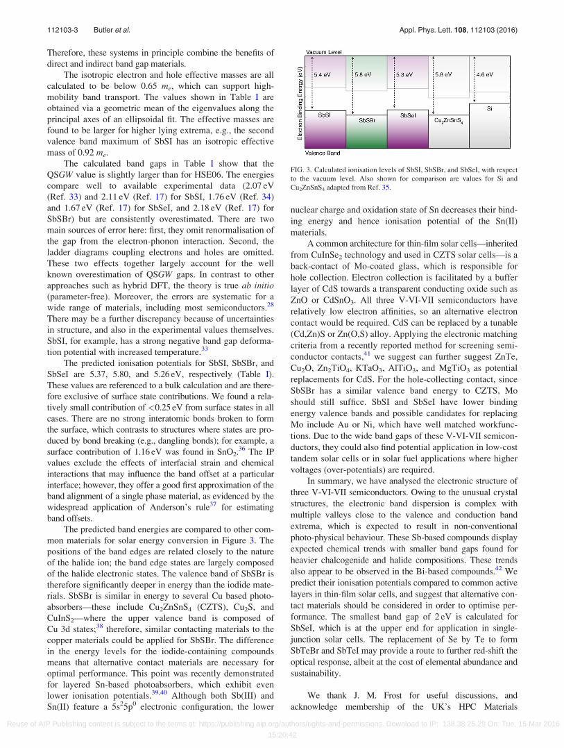
The predicted band energies are compared to other com-
mon materials for solar energy conversion in Figure 3. The
positions of the band edges are related closely to the nature
of the halide ion; the band edge states are largely composed
of the halide electronic states. The valence band of SbSBr is
therefore significantly deeper in energy than the iodide mate-
rials. SbSBr is similar in energy to several Cu based photo-
absorbers—these include Cu2ZnSnS4 (CZTS), Cu2S, and
CuInS2—where the upper valence band is composed of
Cu 3d states;38 therefore, similar contacting materials to the
copper materials could be applied for SbSBr. The difference
in the energy levels for the iodide-containing compounds
means that alternative contact materials are necessary for
optimal performance. This point was recently demonstrated
for layered Sn-based photoabsorbers, which exhibit even
lower ionisation potentials.39,40 Although both Sb(III) and
Sn(II) feature a 5s25p0 electronic configuration, the lower
nuclear charge and oxidation state of Sn decreases their bind-
ing energy and hence ionisation potential of the Sn(II)
materials.
A common architecture for thin-film solar cells—inherited
from CuInSe2 technology and used in CZTS solar cells—is a
back-contact of Mo-coated glass, which is responsible for
hole collection. Electron collection is facilitated by a buffer
layer of CdS towards a transparent conducting oxide such as
ZnO or CdSnO3. All three V-VI-VII semiconductors have
relatively low electron affinities, so an alternative electron
contact would be required. CdS can be replaced by a tunable
(Cd,Zn)S or Zn(O,S) alloy. Applying the electronic matching
criteria from a recently reported method for screening semi-
conductor contacts,41 we suggest can further suggest ZnTe,
Cu2O, Zn2TiO4, KTaO3, AlTiO3, and MgTiO3 as potential
replacements for CdS. For the hole-collecting contact, since
SbSBr has a similar valence band energy to CZTS, Mo
should still suffice. SbSI and SbSeI have lower binding
energy valence bands and possible candidates for replacing
Mo include Au or Ni, which have well matched workfunc-
tions. Due to the wide band gaps of these V-VI-VII semicon-
ductors, they could also find potential application in low-cost
tandem solar cells or in solar fuel applications where higher
voltages (over-potentials) are required.
In summary, we have analysed the electronic structure of
three V-VI-VII semiconductors. Owing to the unusual crystal
structures, the electronic band dispersion is complex with
multiple valleys close to the valence and conduction band
extrema, which is expected to result in non-conventional
photo-physical behaviour. These Sb-based compounds display
expected chemical trends with smaller band gaps found for
heavier chalcogenide and halide compositions. These trends
also appear to be observed in the Bi-based compounds.42 We
predict their ionisation potentials compared to common active
layers in thin-film solar cells, and suggest that alternative con-
tact materials should be considered in order to optimise per-
formance. The smallest band gap of 2 eV is calculated for
SbSeI, which is at the upper end for application in single-
junction solar cells. The replacement of Se by Te to form
SbTeBr and SbTeI may provide a route to further red-shift the
optical response, albeit at the cost of elemental abundance and
sustainability.
We thank J. M. Frost for useful discussions, and
acknowledge membership of the UK’s HPC Materials
FIG. 3. Calculated ionisation levels of SbSI, SbSBr, and SbSeI, with respect
to the vacuum level. Also shown for comparison are values for Si and
Cu2ZnSnS4 adapted from Ref. 35.
112103-3 Butler et al. Appl. Phys. Lett. 108, 112103 (2016)
Reuse of AIP Publishing content is subject to the terms at: https://publishing.aip.org/authors/rights-and-permissions. Download to IP: 138.38.25.29 On: Tue, 15 Mar 2016
15:20:42

Chemistry Consortium, which is funded by EPSRC Grant No.
EP/L000202. The work has also been supported by EPSRC
through Grant Nos. EP/M009580/1, EP/J017361/1, EP/
M009602/1, and EP/M011631/1. This work benefited from
membership of the UK Materials Design Network. Data accessstatement: The crystal structures reported in this work are
available in an on-line repository https://github.com/WMD-
group/Crystal_ structures and the MacroDensity code is
freely available from https://github.com/WMD-group/
MacroDensity.
1M. A. Green, A. Ho-Baillie, and H. J. Snaith, Nat. Photonics 8, 506
(2014).2D. O. Scanlon and A. Walsh, Appl. Phys. Lett. 100, 251911 (2012).3T. Yokoyama, F. Oba, A. Seko, H. Hayashi, Y. Nose, and I. Tanaka, Appl.
Phys. Express 6, 061201 (2013).4J. J. S. Scragg, L. Choubrac, A. Lafond, T. Ericson, and C. Platzer-
Bj€orkman, Appl. Phys. Lett. 104, 041911 (2014).5S. Chen, A. Walsh, X.-G. Gong, and S.-H. Wei, Adv. Mater. 25, 1522
(2013).6T. Gokmen, O. Gunawan, T. K. Todorov, and D. B. Mitzi, Appl. Phys.
Lett. 103, 103506 (2013).7O. Gunawan, T. Gokmen, and D. B. Mitzi, J. Appl. Phys. 116, 084504
(2014).8E. Fatuzzo, G. Harbeke, W. J. W. Merz, R. Nitsche, H. Roetschi, and W.
Ruppel, Phys. Rev. 127, 2036 (1962).9R. Nitsche, H. Roetschi, and P. Wild, Appl. Phys. Lett. 4, 210 (1964).
10D. Berlincourt, H. Jaffe, W. J. Merz, and R. Nitsche, Appl. Phys. Lett. 4,
61 (1964).11V. M. Fridkin, I. I. Groshik, V. A. Lakhovizkaya, M. P. Mikhailov, and V.
N. Nosov, Appl. Phys. Lett. 10, 354 (1967).12A. A. Grekov, A. I. Rodin, and V. M. Fridkin, Appl. Phys. Lett. 14, 119
(1969).13A. Kikuchi, Y. Oka, and E. Sawaguchi, J. Phys. Soc. Jpn. 23, 337 (1967).14J. P. Allen, J. J. Carey, A. Walsh, D. O. Scanlon, and G. W. Watson,
J. Phys. Chem. C 117, 14759 (2013).15D. J. Payne, R. G. Egdell, A. Walsh, G. W. Watson, J. Guo, P.-A. Glans,
T. Learmonth, and K. E. Smith, Phys. Rev. Lett. 96, 157403 (2006).16A. Walsh, D. J. Payne, R. G. Egdell, and G. W. Watson, Chem. Soc. Rev.
40, 4455 (2011).17J. Alward and C. Fong, Solid State Commun. 25, 307 (1978).
18O. M. Madelung, Semiconductors: Data Handbook, 3rd ed. (Springer,
Berlin, 2003), p. 691.19K. T. Butler, J. M. Frost, and A. Walsh, Energy Environ. Sci. 8, 838
(2015).20R. E. Brandt, V. Stevanovic, D. S. Ginley, and T. Buonassisi, MRS
Commun. 5, 265 (2015).21R. Nechache, C. Harnagea, S. Li, L. Cardenas, W. Huang, J. Chakrabartty,
and F. Rosei, Nat. Photonics 9, 61 (2015).22J. M. Frost, K. T. Butler, F. Brivio, C. H. Hendon, M. van Schilfgaarde,
and A. Walsh, Nano Lett. 14, 2584 (2014).23Y. Kutes, L. Ye, Y. Zhou, S. Pang, B. D. Huey, and N. P. Padture, J. Phys.
Chem. Lett. 5, 3335 (2014).24S. N. Rashkeev, F. El-Mellouhi, S. Kais, and F. H. Alharbi, Sci. Rep. 5,
11467 (2015).25J. Heyd and G. Scuseria, J. Chem. Phys. 121, 1187 (2004).26J. Heyd, G. E. Scuseria, and M. Ernzerhof, J. Chem. Phys. 124, 219906
(2006).27A. Maniopoulou, E. R. Davidson, R. Grau-Crespo, A. Walsh, I. J. Bush, C.
R. A. Catlow, and S. M. Woodley, Comput. Phys. Commun. 183, 1696
(2012).28M. Van Schilfgaarde, T. Kotani, and S. Faleev, Phys. Rev. Lett. 96,
226402 (2006).29See http://www.lmsuite.org for Lmsuite; accessed 12 December 2015.30F. Brivio, K. T. Butler, A. Walsh, and M. van Schilfgaarde, Phys. Rev. B
89, 155204 (2014).31K. T. Butler, C. H. Hendon, and A. Walsh, Appl. Mater. Interfaces 6,
22044 (2014).32See supplementary material at http://dx.doi.org/10.1063/1.4943973 for
additional calculation details.33M. Nowak and P. Szperlich, Opt. Mater. 35, 1200 (2013).34T. A. Pikka and V. M. Fridkin, Fiz. Tverd. Tela 10, 2668 (1969).35K. T. Butler, J. M. Frost, and A. Walsh, Mater. Horiz. 2, 228 (2015).36K. T. Butler, J. Buckeridge, C. R. A. Catlow, and A. Walsh, Phys. Rev. B
89, 115320 (2014).37R. Anderson, Solid State Electron. 5, 341 (1962).38S. H. Wei and A. Zunger, J. Appl. Phys. 78, 3846 (1995).39L. A. Burton and A. Walsh, Appl. Phys. Lett. 102, 132111 (2013).40V. Steinmann, R. Jaramillo, K. Hartman, R. Chakraborty, R. E. Brandt, J.
R. Poindexter, Y. S. Lee, L. Sun, A. Polizzotti, H. H. Park, R. G. Gordon,
and T. Buonassisi, Adv. Mater. 26, 7488 (2014).41K. T. Butler, Y. Kumagai, F. Oba, and A. Walsh, J. Mater. Chem. C 4,
1149 (2016).42A. M. Ganose, K. T. Butler, A. Walsh, and D. O. Scanlon, J. Mater. Chem. A
4, 2060 (2016).
112103-4 Butler et al. Appl. Phys. Lett. 108, 112103 (2016)
Reuse of AIP Publishing content is subject to the terms at: https://publishing.aip.org/authors/rights-and-permissions. Download to IP: 138.38.25.29 On: Tue, 15 Mar 2016
15:20:42
Recommended