Date
P P A PThe following PPAP documentation is assembled according to
the AIAG, 4th Edition PPAP Manual and applicable customer requirements
Page 1
Manufacturing Site- Danshui, China
Production Part Approval ProcessThe following PPAP documentation is assembled according to
AIAG, 4th Edition PPAP Manual and applicable customer requirements
TABLE OF CONTENTS
1) Design Recordsa. Customer Specificationb. Vishay Data Sheetc. SMD Magnetics Packaging Methodsd. Vishay Cross Section Photographe. Certificate of Design Constructionf. Standards of Manufacture for IHLP Inductors
2) Engineering Change Documents, if any
3) Customer Engineering Approval, if needed
4) Design FMEA
5) Process Flow Chart
6) Process FMEA
7) Control Plan
8) Measurement System Analysis Studiesa. Inductance Measurement Systemb. “Q” Measurement Systemc. DC Resistance Measurement System
9) Dimensional Results
10) Material Performance Test Results
Page 3

Production Part Approval ProcessThe following PPAP documentation is assembled according to
AIAG, 4th Edition PPAP Manual and applicable customer requirements
TABLE OF CONTENTS
11) Initial Process Studies
12) Qualified Laboratory Documentationa. Beer Sheva, Israelb. Yankton, SDc. Columbus, NE
13) Appearance Approval Report (AAR), if applicable
14) Sample Product
15) Master Sample
16) Checking Aids
17) Records of Compliance with Customer Specific Requirements
18) Part Submission Warrant (PSW)
19) Bulk Material Requirements
Page 4
Note: Generic PPAPs do not include all sections shown in the Table of Contents. Sections 4,5,6,7,8,12,&18 are only available upon request of a full Automotive PPAP.

Production Part Approval ProcessThe following PPAP documentation is assembled according to
AIAG, 4th Edition PPAP Manual and applicable customer requirements
Use the control buttons below to navigate through the PPAP sections.
Section 1. Design Records
Page 5

IHLD-3232HB-5Awww.vishay.com Vishay Dale
Revision: 20-Oct-17 1 Document Number: 34383For technical questions, contact: [email protected]
THIS DOCUMENT IS SUBJECT TO CHANGE WITHOUT NOTICE. THE PRODUCTS DESCRIBED HEREIN AND THIS DOCUMENTARE SUBJECT TO SPECIFIC DISCLAIMERS, SET FORTH AT www.vishay.com/doc?91000
Low Profile, High Current Dual Inductors
DESIGN SUPPORT TOOLS click logo to get started
Notes
• All test data is referenced to 25 °C ambient• Operating temperature range -55 °C to +155 °C• The part temperature (ambient + temp. rise) should not exceed
155 °C under worst case operating conditions. Circuit design, component placement, PWB trace size and thickness, airflow and other cooling provisions all affect the part temperature. Part temperature should be verified in the end application
• Rated operating voltage (across inductor) = 50 V(1) DC current (A) that will cause an approximate T of 40 °C(2) DC current (A) that will cause L0 to drop approximately 20 %
FEATURES• Two inductors in one package• High temperature, up to 155 °C• Shielded construction• Optimal design realizes high quality sound and
low distortion• Low coupling for minimal cross-talk between
inductors• Frequency range up to 1 MHz• Lowest DCR/μH, in this package size• Handles high transient current spikes without saturation• Ultra-low buzz noise, due to composite construction• AEC-Q200 qualified• IHLP design. PATENT(S): www.vishay.com/patents• Material categorization: for definitions of compliance
please see www.vishay.com/doc?99912
APPLICATIONS• Class D audio amplifiers
PATENT(S): www.vishay.com/patentsThis Vishay product is protected by one or more United States and international patents.
STANDARD ELECTRICAL SPECIFICATIONSL0
INDUCTANCE
± 20 %
AT 100 kHz,
0.25 V, 0 A
(μH)
DCR
TYP.
25 °C
(m )
DCR
MAX.
25 °C
(m )
HEAT
RATING
CURRENT
DC TYP.
(A) (1)
SATURATION
CURRENT
DC TYP.
(A) (2)
SRF
TYP.
(MHz)
5 27.3 29.2 6.0 8.5 18.0
10 50.0 53.50 5.0 5.2 13.0
15 62.0 66.34 4.2 3.5 10.0
22 103.0 110.21 3.3 2.9 9.0
33 149.0 159.43 2.4 2.9 6.1
AvailableDesign Tools
DIMENSIONS in inches [millimeters]
RECOMMENDED PAD LAYOUT0.110 (2.79)
0.372 (9.45)
0.040 (1.02)
0.131 (3.33)
0.1200 (3.05)
0.379 ± 0.010(9.627 ± 0.254)
0.342 ± 0.010(8.687 ± 0.254)
0.360 ± 0.005(9.144 ± 0.127)
0.384 ± 0.010(9.754 ± 0.254)
0.060 ± 0.005(1.524 ± 0.127)
0.070 ± 0.005(1.778 ± 0.127)
0.103 ± 0.010(2.616 ± 0.254)
DESCRIPTION
IHLD-3232HB-5A 10 μH ± 20 % ER e3
MODEL INDUCTANCE VALUE INDUCTANCE TOLERANCE PACKAGE CODE JEDEC® LEAD (Pb)-FREE STANDARD
GLOBAL PART NUMBER
I H L D 3 2 3 2 H B E R 1 0 0 M 5 A
PRODUCT FAMILY SIZE PACKAGECODE
INDUCTANCEVALUE
TOL. SERIES

IHLD-3232HB-5Awww.vishay.com Vishay Dale
Revision: 20-Oct-17 2 Document Number: 34383For technical questions, contact: [email protected]
THIS DOCUMENT IS SUBJECT TO CHANGE WITHOUT NOTICE. THE PRODUCTS DESCRIBED HEREIN AND THIS DOCUMENTARE SUBJECT TO SPECIFIC DISCLAIMERS, SET FORTH AT www.vishay.com/doc?91000
PERFORMANCE GRAPHS
0
20
40
60
80
100
0.0
2.0
4.0
6.0
8.0
10.0
0 2 4 6 8 10
TE
MP
ER
AT
UR
E (°C
)
IND
UC
TA
NC
E (μ
H)
DC CURRENT (A)
5 μH
L
ΔT °C
0
20
40
60
80
100
0.0
4.0
8.0
12.0
16.0
20.0
0 2 4 6 8
TE
MP
ER
AT
UR
E (°C
)
IND
UC
TA
NC
E (μ
H)
DC CURRENT (A)
10 μH
L
ΔT °C
0
20
40
60
80
100
0.0
4.0
8.0
12.0
16.0
20.0
0 2 4 6 8
TE
MP
ER
AT
UR
E (°C
)
IND
UC
TA
NC
E (μ
H)
DC CURRENT (A)
15 μH
L
ΔT °C
0
20
40
60
80
100
0.0
5.0
10.0
15.0
20.0
25.0
0 1 2 3 4 5
TE
MP
ER
AT
UR
E (°C
)
IND
UC
TA
NC
E (μ
H)
DC CURRENT (A)
5A 22 μHL
ΔT °C
0
20
40
60
80
100
0.0
8.0
16.0
24.0
32.0
40.0
0 1 2 3 4
TE
MP
ER
AT
UR
E (°C
)
IND
UC
TA
NC
E (μ
H)
DC CURRENT (A)
33 μH
L ΔT °C

IHLD-3232HB-5Awww.vishay.com Vishay Dale
Revision: 20-Oct-17 3 Document Number: 34383For technical questions, contact: [email protected]
THIS DOCUMENT IS SUBJECT TO CHANGE WITHOUT NOTICE. THE PRODUCTS DESCRIBED HEREIN AND THIS DOCUMENTARE SUBJECT TO SPECIFIC DISCLAIMERS, SET FORTH AT www.vishay.com/doc?91000
PERFORMANCE GRAPHS: INDUCTANCE AND Q VS. FREQUENCY
0
20
40
60
80
100
0
10
20
30
40
50
0.1 1 10 100
Q
IND
UC
TA
NC
E (μ
H)
FREQUENCY (MHz)
5 μH
L
Q
0
20
40
60
80
100
0
10
20
30
40
50
0.1 1 10 100
Q
IND
UC
TA
NC
E (μ
H)
FREQUENCY (MHz)
10 μH
LQ
0
20
40
60
80
100
0
20
40
60
80
100
0.1 1 10 100
Q
IND
UC
TA
NC
E (μ
H)
FREQUENCY (MHz)
15 μH
LQ
0
10
20
30
40
50
60
0
20
40
60
80
100
120
0.1 1 10
Q
IND
UC
TA
NC
E (μ
H)
FREQUENCY (MHz)
22 μH
LQ
0
10
20
30
40
50
60
0
30
60
90
120
150
180
0.1 1 10
Q
IND
UC
TA
NC
E (μ
H)
FREQUENCY (MHz)
33 μH
L
Q

Legal Disclaimer Noticewww.vishay.com Vishay
Revision: 02-Oct-12 1 Document Number: 91000
Disclaimer
ALL PRODUCT, PRODUCT SPECIFICATIONS AND DATA ARE SUBJECT TO CHANGE WITHOUT NOTICE TO IMPROVERELIABILITY, FUNCTION OR DESIGN OR OTHERWISE.
Vishay Intertechnology, Inc., its affiliates, agents, and employees, and all persons acting on its or their behalf (collectively,“Vishay”), disclaim any and all liability for any errors, inaccuracies or incompleteness contained in any datasheet or in any otherdisclosure relating to any product.
Vishay makes no warranty, representation or guarantee regarding the suitability of the products for any particular purpose orthe continuing production of any product. To the maximum extent permitted by applicable law, Vishay disclaims (i) any and allliability arising out of the application or use of any product, (ii) any and all liability, including without limitation special,consequential or incidental damages, and (iii) any and all implied warranties, including warranties of fitness for particularpurpose, non-infringement and merchantability.
Statements regarding the suitability of products for certain types of applications are based on Vishay’s knowledge of typicalrequirements that are often placed on Vishay products in generic applications. Such statements are not binding statementsabout the suitability of products for a particular application. It is the customer’s responsibility to validate that a particularproduct with the properties described in the product specification is suitable for use in a particular application. Parametersprovided in datasheets and/or specifications may vary in different applications and performance may vary over time. Alloperating parameters, including typical parameters, must be validated for each customer application by the customer’stechnical experts. Product specifications do not expand or otherwise modify Vishay’s terms and conditions of purchase,including but not limited to the warranty expressed therein.
Except as expressly indicated in writing, Vishay products are not designed for use in medical, life-saving, or life-sustainingapplications or for any other application in which the failure of the Vishay product could result in personal injury or death.Customers using or selling Vishay products not expressly indicated for use in such applications do so at their own risk. Pleasecontact authorized Vishay personnel to obtain written terms and conditions regarding products designed for such applications.
No license, express or implied, by estoppel or otherwise, to any intellectual property rights is granted by this document or byany conduct of Vishay. Product names and markings noted herein may be trademarks of their respective owners.
Material Category Policy
Vishay Intertechnology, Inc. hereby certifies that all its products that are identified as RoHS-Compliant fulfill the
definitions and restrictions defined under Directive 2011/65/EU of The European Parliament and of the Council
of June 8, 2011 on the restriction of the use of certain hazardous substances in electrical and electronic equipment
(EEE) - recast, unless otherwise specified as non-compliant.
Please note that some Vishay documentation may still make reference to RoHS Directive 2002/95/EC. We confirm that
all the products identified as being compliant to Directive 2002/95/EC conform to Directive 2011/65/EU.
Vishay Intertechnology, Inc. hereby certifies that all its products that are identified as Halogen-Free follow Halogen-Free
requirements as per JEDEC JS709A standards. Please note that some Vishay documentation may still make reference
to the IEC 61249-2-21 definition. We confirm that all the products identified as being compliant to IEC 61249-2-21
conform to JEDEC JS709A standards.

Packaging Methodswww.vishay.com Vishay Dale
Revision: 11-Apr-16 1 Document Number: 34150For technical questions, contact: [email protected]
THIS DOCUMENT IS SUBJECT TO CHANGE WITHOUT NOTICE. THE PRODUCTS DESCRIBED HEREIN AND THIS DOCUMENTARE SUBJECT TO SPECIFIC DISCLAIMERS, SET FORTH AT www.vishay.com/doc?91000
SMD Magnetics Packaging Methods
TAPE AND REEL in inches [millimeters] - Meets EIA RS-481 tape and reel packaging standard
MODEL
PACKAGE CODE
REELSIZE
CARRIERTAPE
WIDTH(W)
COMPONENTPITCH
(P)UNITS/REEL
PACKAGE CODE
UNITS/BULK
PREVIOUSCODE
GLOBALCODE
LEAD (Pb)- BEARING
GLOBALCODELEAD
(Pb)-FREEPREVIOUS
CODE
GLOBALCODELEAD (Pb)-
BEARING
GLOBALCODELEAD
(Pb)-FREE
IHLP-1212ABER - - ER 13 0.472 [12.0] 0.315 [8.0] 3000 - - - -
IHLP-1212ABEV - - ER 13 0.472 [12.0] 0.315 [8.0] 4000 - - - -
IHLP-1212AEER - - ER 13 0.472 [12.0] 0.315 [8.0] 3000 - - - -
IHLP-1212BZER - - ER 13 0.472 [12.0] 0.315 [8.0] 3000 - - - -
IHLP-1212BZEV - - ER 13 0.472 [12.0] 0.315 [8.0] 4000 - - - -
IHLP-1616AB - - ER 13 0.472 [12.0] 0.315 [8.0] 4000 - - EB 100
IHLP-1616BZ - - ER 13 0.472 [12.0] 0.315 [8.0] 4000 - - EB 100
IHLP-2020AB - - ER 13 0.472 [12.0] 0.315 [8.0] 4000 - - EB 100
IHLP-2020BZ - - ER 13 0.472 [12.0] 0.315 [8.0] 2000 - - EB 100
IHLP-2020CZ - - ER 13 0.472 [12.0] 0.315 [8.0] 2000 - - EB 100
IHLP-2525AH - - ER 13 0.630 [16.0] 0.315 [8.0] 2000 - - EB 100
IHLP-2525BD - - ER 13 0.630 [16.0] 0.315 [8.0] 2000 - - EB 100
IHLP-2525CZ - - ER 13 0.630 [16.0] 0.315 [8.0] 2000 - - EB 100
IHLP-2525EZ - - ER 13 0.630 [16.0] 0.472 [12.0] 500 - - EB 100
IHLP-3232CZ - - ER 13 0.630 [16.0] 0.472 [12.0] 1000 - - EB 100
IHLP-3232DZ - - ER 13 0.630 [16.0] 0.472 [12.0] 500 - - EB 100
IHLP-4040DZ - - ER 13 0.945 [24.0] 0.630 [16.0] 500 - - EB 100
IHLP-5050CE - - ER 13 0.945 [24.0] 0.630 [16.0] 500 - - EB 100
IHLP-5050EZ - - ER 13 0.945 [24.0] 0.630 [16.0] 250 - - EB 100
IHLP-5050FD - - ER 13 0.945 [24.0] 0.630 [16.0] 250 - - EB 100
IHLP-6767DZ - - ER 13 0.945 [24.0] 0.945 [24.0] 250 - - EB 100
IHLP-6767GZ - - ER 13 0.945 [24.0] 0.945 [24.0] 200 - - EB 100
IHLP-8787MZ - - ER 13 1.73 [44.0] 1.26 [32.0] 100 - - - -
IHCL-4040DZ - - ER 13 0.945 [24.0] 0.630 [16.0] 500 - - EB 100
IHLD-4032KB - - ER 13 0.945 [24.0] 0.630 [16.0] 250 - - EB 100
IHLD-3232HB - - ER 13 0.945 [24.0] 0.630 [16.0] 250 - - EB 100
IHLE-2525CD - - ER 13 0.630 [16.0] 0.315 [8.0] 2000 - - EB 100
IHLE-3232DD - - ER 13 0.630 [16.0] 0.472 [12.0] 500 - - EB 100
IHLE-4040DD - - ER 13 0.945 [24.0] 0.630 [16.0] 500 - - EB 100
IHLR-4040DZ - - ER 13 0.945 [24.0] 0.630 [16.0] 500 - - EB 100
IHLM-2525CZ - - ER 13 0.630 [16.0] 0.315 [8.0] 2000 - - EB 100
IHLW-4040CF - - ER 13 0.945 [24.0] 0.630 [16.0] 500 - - EB 100
IHLW-5050CE - - ER 13 0.945 [24.0] 0.630 [16.0] 500 - - EB 100
IFLP-4040DZ - - ER 13 0.945 [24.0] 0.630 [16.0] 500 - - EB 100
IFLR-2727EZ - - ER 13 0.630 [16.0] 0.630 [16.0] 1000 - - - -
IFLR-4027EZ - - ER 13 0.945 [24.0] 0.630 [16.0] 1000 - - - -
IFLR-4031GC - - ER 13 0.945 [24.0] 0.472 [12.0] 500 - - EB 100
IFLR-5151HZ - - ER 13 0.945 [24.0] 0.630 [16.0] 450 - - EB 100
User Direction of Feed Carrier Dimensions
P
W

Packaging Methodswww.vishay.com Vishay Dale
Revision: 11-Apr-16 2 Document Number: 34150For technical questions, contact: [email protected]
THIS DOCUMENT IS SUBJECT TO CHANGE WITHOUT NOTICE. THE PRODUCTS DESCRIBED HEREIN AND THIS DOCUMENTARE SUBJECT TO SPECIFIC DISCLAIMERS, SET FORTH AT www.vishay.com/doc?91000
MODEL
PACKAGE CODE
REELSIZE
CARRIERTAPE
WIDTH(W)
COMPONENTPITCH
(P)UNITS/REEL
PACKAGE CODE
UNITS/BULK
PREVIOUSCODE
GLOBAL
CODE
LEAD (Pb)-
BEARING
GLOBAL
CODE
LEAD
(Pb)-FREEPREVIOUS
CODE
GLOBAL
CODE
LEAD
(Pb)-
BEARING
GLOBAL
CODE
LEAD
(Pb)-FREE
IFSC-0806AZ - - ER 7 0.315 [8.0] 0.157 [4.0] 2000 - - - -
IFSC-1008AB - - ER 7 0.315 [8.0] 0.157 [4.0] 2000 - - - -
IFSC-1111AZ - - ER 7 0.315 [8.0] 0.157 [4.0] 2000 - - - -
IFSC-1111AB - - ER 7 0.315 [8.0] 0.157 [4.0] 2000 - - - -
IFSC-1515AH - - ER 13 0.472 [12.0] 0.315 [8.0] 2000 - - - -
IHHP-0806AZ-01 - - ER 7 0.315 [8.0] 0.157 [4.0] 2000 - - - -
IHHP-0806AB-01 - - ER 7 0.315 [8.0] 0.157 [4.0] 2000 - - - -
IHHP-1008AZ-01 - - ER 7 0.315 [8.0] 0.157 [4.0] 3000 - - - -
IHHP-1008AB-01 - - ER 7 0.315 [8.0] 0.157 [4.0] 3000 - - - -
IHHP-1212ZH-01 - - ER 7 0.315 [8.0] 0.157 [4.0] 3000 - - - -
IHHP-1212AZ-01 - - ER 7 0.315 [8.0] 0.157 [4.0] 3000 - - - -
IHSM-3825 RC2 RE ER 13 0.945 [24.0] 0.472 [12.0] 750 P09 PJ EB 100
IHSM-4825 RC2 RE ER 13 0.945 [24.0] 0.472 [12.0] 750 P09 PJ EB 100
IHSM-5832 RC3 RF ER 13 1.26 [32.0] 0.472 [12.0] 500 P09 PJ EB 100
IHSM-7832 RC4 RG ER 13 1.73 [44.0] 0.472 [12.0] 500 P09 PJ EB 100
IDC-2512 - - ER 13 0.630 [16.0] 0.315 [8.0] 2000 - - - -
IDC-5020 - - ER 13 0.630 [16.0] 0.472 [12.0] 500 - - - -
IDC-7328 - - ER 13 0.945 [24.0] 0.945 [24.0] 250 - - - -
IDCS-2512 - - ER 13 0.630 [16.0] 0.315 [8.0] 2000 - - - -
IDCS-5020 - - ER 13 0.630 [16.0] 0.472 [12.0] 500 - - - -
IDCS-7328 - - ER 13 0.945 [24.0] 0.945 [24.0] 250 - - - -
IDCP-1813 - - ER 13 0.472 [12.0] 0.315 [8.0] 2000 - - - -
IDCP-2218 - - ER 13 0.472 [12.0] 0.315 [8.0] 1500 - - - -
IDCP-3114 - - ER 13 0.630 (16.0) 0.472 [12.0] 1000 - - - -
IDCP-3020 - - ER 13 0.630 (16.0) 0.472 [12.0] 1000 - - - -
IDCP-3722 - - ER 13 0.945 [24.0] 0.472 [12.0] 500 - - - -
IDCP-3916 - - ER 13 0.945 [24.0] 0.472 [12.0] 500 - - - -
IFCB-0402 - - ER 7 0.315 [8.0] 0.079 [2.0] 10 000 - - - -
ILC-0402 - - ER 7 0.315 [8.0] 0.079 [2.0] 10 000 - - - -
ILC-0603 - - ER 7 0.315 [8.0] 0.157 [4.0] 4000 - - - -
ILC-0805 - - ER 7 0.315 [8.0] 0.157 [4.0] 4000 - - - -
IMC-0402 - - ER 7 0.315 [8.0] 0.079 [2.0] 10 000 - - - -
IMC-0402-01 - - ER 7 0.315 [8.0] 0.079 [2.0] 10 000 - - - -
IMC-0603 - - ER 7 0.315 [8.0] 0.157 [4.0] 4000 - - - -
IMC-0603-01 - - ER 7 0.315 [8.0] 0.079 [2.0] 3000 - - - -
IMC-0805-01 - - ER 7 0.315 [8.0] 0.157 [4.0] 2000 - - - -
IMC-1008 - - ER 7 0.315 [8.0] 0.157 [4.0] 2000 - - - -
IMC-1210 R98/RB3R99/RB4
SY/ANSZ/R9
ER/ETES/EU
713
0.315 [8.0]0.315 [8.0]
0.157 [4.0]0.157 [4.0]
20007500 B13 BN EB 500
IMC-1210-100 R98/RB3R99/RB4
SY/ANSZ/R9
ER/ETES/EU
713
0.315 [8.0]0.315 [8.0]
0.157 [4.0]0.157 [4.0]
20007500 B13 BN EB 500
IMC-1812 R73/R92R13/R91
RV/RXRQ/RW
ER/ETES/EU
713
0.472 [12.0]0.472 [12.0]
0.315 [8.0]0.315 [8.0]
5002000 B13 BN EB 500
IMCH-1812 - - ER 7 0.472 [12.0] 0.315 [8.0] 500 - - - -
IMC-2220 - - ER 13 0.630 [16.0] 0.472 [12.0] 1000 - - - -
TAPE AND REEL in inches [millimeters] - Meets EIA RS-481 tape and reel packaging standard

Production Part Approval ProcessThe following PPAP documentation is assembled according toAIAG, 4th Edition PPAP Manual and applicable customer requirements
Cross Section Photo
IHLD3232HBER100M5A
1

Production Part Approval ProcessThe following PPAP documentation is assembled according to
AIAG, 4th Edition PPAP Manual and applicable customer requirements
Use the control buttons below to navigate through the PPAP sections.
Section 2: Engineering Change Documents
There are no applicable Engineering Change Documents for this part number.
Page 24
Production Part Approval ProcessThe following PPAP documentation is assembled according to
AIAG, 4th Edition PPAP Manual and applicable customer requirements
Use the control buttons below to navigate through the PPAP sections.
Section 3: Customer Engineering Approval
Customer Engineering Approval does not apply for this part number
Page 25

IHLD3232HBER M5ADIMENSIONAL ANALYSIS
12
3
4
57
6
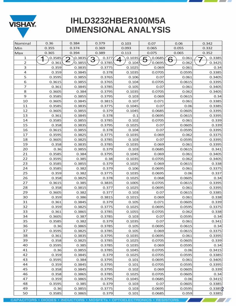
IHLD3232HBER100M5ADIMENSIONAL ANALYSIS
Nominal 0.36 0.384 0.379 0.103 0.07 0.06 0.342Min 0.355 0.374 0.369 0.093 0.065 0.055 0.332Max 0.365 0.394 0.389 0.113 0.075 0.065 0.352
1 0.3585 0.3835 0.377 0.1035 0.0685 0.061 0.33852 0.361 0.3855 0.3785 0.104 0.0695 0.062 0.34253 0.359 0.3835 0.3775 0.1025 0.069 0.061 0.344 0.359 0.3845 0.378 0.1035 0.0705 0.0595 0.33855 0.3595 0.3855 0.3765 0.106 0.07 0.061 0.34056 0.3615 0.3855 0.3765 0.104 0.0705 0.0615 0.33957 0.361 0.3845 0.3785 0.105 0.07 0.061 0.34058 0.3605 0.384 0.3795 0.1035 0.0705 0.062 0.34059 0.3585 0.3855 0.3795 0.103 0.069 0.0615 0.3410 0.3605 0.3845 0.3815 0.107 0.071 0.061 0.338511 0.3585 0.3835 0.3775 0.1045 0.07 0.06 0.338512 0.3605 0.3855 0.379 0.1045 0.0685 0.0605 0.339513 0.361 0.3845 0.378 0.1 0.0695 0.0615 0.339514 0.3585 0.3855 0.3785 0.102 0.0705 0.061 0.33915 0.358 0.3835 0.3795 0.1025 0.07 0.0605 0.33916 0.3615 0.3855 0.378 0.104 0.07 0.0595 0.339517 0.3595 0.3825 0.3775 0.1035 0.069 0.062 0.337518 0.3605 0.3825 0.3785 0.103 0.07 0.0595 0.339519 0.358 0.3835 0.3785 0.1035 0.069 0.061 0.339520 0.36 0.3855 0.379 0.103 0.0685 0.0615 0.34121 0.3585 0.384 0.3795 0.1045 0.069 0.061 0.340522 0.3595 0.385 0.38 0.1035 0.0705 0.062 0.340523 0.3585 0.3855 0.379 0.1025 0.069 0.0615 0.33824 0.3585 0.382 0.379 0.106 0.0695 0.061 0.337525 0.359 0.382 0.3775 0.1035 0.0695 0.06 0.33726 0.358 0.3825 0.378 0.1025 0.068 0.0605 0.3427 0.3615 0.385 0.3835 0.1005 0.0705 0.0615 0.339528 0.358 0.3815 0.377 0.1025 0.0695 0.061 0.339529 0.3605 0.382 0.377 0.103 0.07 0.0615 0.338530 0.359 0.386 0.3815 0.1015 0.069 0.061 0.33831 0.361 0.3845 0.379 0.105 0.071 0.0605 0.33932 0.359 0.3825 0.3775 0.1025 0.0695 0.0595 0.337533 0.361 0.3865 0.3785 0.1055 0.0705 0.062 0.33834 0.3605 0.387 0.3785 0.103 0.07 0.0595 0.3435 0.3585 0.382 0.379 0.1035 0.07 0.061 0.34136 0.36 0.3865 0.3785 0.105 0.0695 0.0615 0.3437 0.3595 0.3825 0.3785 0.105 0.069 0.0615 0.337538 0.361 0.3835 0.3795 0.1035 0.0695 0.061 0.339539 0.358 0.3825 0.3785 0.1025 0.0705 0.0605 0.33940 0.3595 0.385 0.3785 0.1035 0.069 0.0595 0.3441 0.36 0.3855 0.3785 0.1045 0.0705 0.06 0.341542 0.359 0.3845 0.379 0.1025 0.0705 0.0595 0.338543 0.3595 0.384 0.3795 0.101 0.0695 0.061 0.340544 0.359 0.3845 0.3795 0.101 0.0705 0.0595 0.339545 0.358 0.3845 0.3795 0.102 0.069 0.0605 0.33946 0.358 0.3865 0.3785 0.1025 0.0705 0.0605 0.3447 0.359 0.3865 0.3795 0.1045 0.0685 0.06 0.341548 0.3595 0.385 0.379 0.103 0.07 0.0605 0.338549 0.36 0.3855 0.3775 0.103 0.0695 0.0595 0.338550 0.3585 0.3865 0.379 0.101 0.0685 0.059 0.3385
1 2 3 4 5 6 7
2

IHLD3232HBER100M5ADIMENSIONAL ANALYSIS
464136312621161161
0.364
0.360
0.356
Ind
ivid
ual
Val
ue
_X=0.35949
UCL=0.363289
LCL=0.355691
464136312621161161
0.004
0.002
0.000
Mo
vin
g R
ang
e
__MR=0.001429
UCL=0.004668
LCL=0
5045403530
0.362
0.360
0.358
Observation
Val
ues
0.364
5
0.363
0
0.361
5
0.360
0
0.358
5
0.357
0
0.355
5
LSL 0.355USL 0.365
Specifications
LSL USL
OverallWithin
0.3620.3600.3580.356
StDev 0.001266Cp 1.32Cpk 1.18PPM 202.87
WithinStDev 0.001100Pp 1.52Ppk 1.36Cpm *PPM 22.46
OverallOverall
Within
Specs
Dimensional Analysis, IHLD3232HBER100M5A, .360 +/- .005 DimensionI Chart
Moving Range Chart
Last 25 Observations
Capability Histogram
Normal Prob PlotAD: 1.238, P: < 0.005
Capability Plot
3

IHLD3232HBER100M5ADIMENSIONAL ANALYSIS
464136312621161161
0.388
0.384
0.380
Ind
ivid
ual
Val
ue
_X=0.38439
UCL=0.388515
LCL=0.380265
464136312621161161
0.004
0.002
0.000
Mo
vin
g R
ang
e
__MR=0.001551
UCL=0.005068
LCL=0
5045403530
0.386
0.384
0.382
Observation
Val
ues
0.3930.3900.3870.3840.3810.3780.375
LSL 0.375USL 0.395
Specifications
LSL USL
OverallWithin
0.38750.38500.38250.3800
StDev 0.001375Cp 2.42Cpk 2.28PPM 0.00
WithinStDev 0.001461Pp 2.28Ppk 2.14Cpm *PPM 0.00
OverallOverall
Within
Specs
Dimensional Analysis, IHLD3232HBER100M5A, .385 +/- .010 DimensionI Chart
Moving Range Chart
Last 25 Observations
Capability Histogram
Normal Prob PlotAD: 0.997, P: 0.011
Capability Plot
4

IHLD3232HBER100M5ADIMENSIONAL ANALYSIS
464136312621161161
0.384
0.380
0.376
Indi
vidu
al V
alue
_X=0.37869
UCL=0.381730
LCL=0.375650
464136312621161161
0.0050
0.0025
0.0000
Mov
ing
Rang
e
__MR=0.001143
UCL=0.003734
LCL=0
5045403530
0.382
0.380
0.378
Observation
Val
ues
0.387
2
0.384
0
0.380
8
0.377
6
0.374
4
0.371
2
LSL 0.369USL 0.389
Specifications
LSL USL
OverallWithin
0.38250.38000.37750.3750
StDev 0.001013Cp 3.29Cpk 3.19PPM 0.00
WithinStDev 0.001249Pp 2.67Ppk 2.59Cpm *PPM 0.00
OverallOverall
Within
Specs
1
1
1
1
1
Dimsional Analysis, IHLD3232HBER100M5A, .379 +/- .010 DimensionI Chart
Moving Range Chart
Last 25 Observations
Capability Histogram
Normal Prob PlotAD: 1.481, P: < 0.005
Capability Plot
5

IHLD3232HBER100M5ADIMENSIONAL ANALYSIS
464136312621161161
0.108
0.104
0.100Indi
vidu
al V
alue
_X=0.10333
UCL=0.107265
LCL=0.099395
464136312621161161
0.004
0.002
0.000
Mov
ing
Rang
e
__MR=0.001480
UCL=0.004834
LCL=0
5045403530
0.104
0.102
0.100
Observation
Val
ues
0.1110.1080.1050.1020.0990.0960.093
LSL 0.093USL 0.113
Specifications
LSL USL
OverallWithin
0.1060.1040.1020.100
StDev 0.001312Cp 2.54Cpk 2.46PPM 0.00
WithinStDev 0.001438Pp 2.32Ppk 2.24Cpm *PPM 0.00
OverallOverall
Within
Specs
Dimensional Analysis, IHLD3232HBER100M5A, .103 +/-.010 DimensionI Chart
Moving Range Chart
Last 25 Observations
Capability Histogram
Normal Prob PlotAD: 0.550, P: 0.149
Capability Plot
6

IHLD3232HBER100M5ADIMENSIONAL ANALYSIS
464136312621161161
0.072
0.070
0.068Indi
vidu
al V
alue
_X=0.06967
UCL=0.072275
LCL=0.067065
464136312621161161
0.0030
0.0015
0.0000
Mov
ing
Rang
e
__MR=0.000980
UCL=0.003201
LCL=0
5045403530
0.0705
0.0695
0.0685
Observation
Val
ues
0.073
6
0.072
0
0.070
4
0.068
8
0.067
2
0.065
6
LSL 0.065USL 0.075
Specifications
LSL USL
OverallWithin
0.0720.0700.068
StDev 0.0008684Cp 1.92Cpk 1.79PPM 0.04
WithinStDev 0.0007465Pp 2.23Ppk 2.09Cpm *PPM 0.00
OverallOverall
Within
Specs
Dimensional Analysis, IHLD323HBER100M5A, .070 +/- .005 DimensionI Chart
Moving Range Chart
Last 25 Observations
Capability Histogram
Normal Prob PlotAD: 1.319, P: < 0.005
Capability Plot
7

IHLD3232HBER100M5ADIMENSIONAL ANALYSIS
464136312621161161
0.062
0.060
0.058
Indi
vidu
al V
alue
_X=0.06072
UCL=0.063108
LCL=0.058332
464136312621161161
0.0030
0.0015
0.0000
Mov
ing
Rang
e
__MR=0.000898
UCL=0.002934
LCL=0
5045403530
0.0624
0.0612
0.0600
Observation
Val
ues
0.064
0
0.062
4
0.060
8
0.059
2
0.057
6
0.056
0
LSL 0.055USL 0.065
Specifications
LSL USL
OverallWithin
0.0620.0600.058
StDev 0.0007961Cp 2.09Cpk 1.79PPM 0.04
WithinStDev 0.0008278Pp 2.01Ppk 1.72Cpm *PPM 0.12
OverallOverall
Within
Specs
Dimensional Analysis, IHLD3232HBER100M5A, .060 +/-.005 DimensionI Chart
Moving Range Chart
Last 25 Observations
Capability Histogram
Normal Prob PlotAD: 1.480, P: < 0.005
Capability Plot
8

IHLD3232HBER100M5ADIMENSIONAL ANALYSIS
464136312621161161
0.342
0.339
0.336
Indi
vidu
al V
alue
_X=0.33936
UCL=0.342454
LCL=0.336266
464136312621161161
0.004
0.002
0.000
Mov
ing
Rang
e
__MR=0.001163
UCL=0.003801
LCL=0
5045403530
0.342
0.340
0.338
Observation
Val
ues
0.3510.3480.3450.3420.3390.3360.333
LSL 0.332USL 0.352
Specifications
LSL USL
OverallWithin
0.34250.34000.33750.3350
StDev 0.001031Cp 3.23Cpk 2.38PPM 0.00
WithinStDev 0.001174Pp 2.84Ppk 2.09Cpm *PPM 0.00
OverallOverall
Within
Specs
1
1
Dimensional Analysis, IHLD3232HBER100M5A, .342 +/- .010 DimensionI Chart
Moving Range Chart
Last 25 Observations
Capability Histogram
Normal Prob PlotAD: 0.502, P: 0.197
Capability Plot
9

SECTION 10PERFORMANCE TEST RESULTSIHLD3232HB-5A
DANSHUI, CHINA MANUFACTURING LOCATION

2
IHLD3232HBER100M5A
Test # Description Ref. Spec Meth / Cond Test Conditions End Point Requirements
Sample Size
Meas Temp
Summary Statistics
0 Preconditioning for lead-free products
AEC-Q200 Rev C - Pb Free Specific Tests Table 4.2
As specified in sections 4.3.1 thru 4.3.3 except Visual per DPS-11,865 10X magnification
N/A 552 N/A N/A
% %Maximum 3.846 4.589Minimum -5.651 -6.696
Mean -0.1769 -1.1981Std Dev 4.9118 5.6481
Initial Final % Initial Final % Initial Final % Initial Final %Maximum 10.2039 10.8719 6.994 34.110 33.540 0.479 10.2902 10.8703 6.765 34.170 33.450 0.662Minimum 8.5749 9.0444 3.930 32.960 32.300 -3.958 8.4515 8.8953 4.670 32.820 32.380 -3.630
Mean 9.46401 10.01676 5.8234 33.3529 32.8138 -1.6108 9.32283 9.85452 5.6911 33.3286 32.8175 -1.5267Std Dev 0.51264 0.57436 0.5913 0.2568 0.2558 1.0537 0.51654 0.56796 0.4535 0.2887 0.2330 1.0410
Initial Final % Initial Final % Initial Final % Initial Final %Maximum 10.2787 10.9413 7.010 48.590 48.930 1.158 10.3824 10.9534 6.692 48.530 48.890 1.292Minimum 8.6248 9.1256 4.621 47.450 47.100 -1.644 8.5167 8.9690 4.694 47.230 47.220 -1.036
Mean 9.53206 10.09727 5.9159 48.0496 47.9043 -0.3028 9.39800 9.93582 5.7129 48.0157 47.9105 -0.2187Std Dev 0.51703 0.57367 0.5682 0.2263 0.4105 0.6624 0.52145 0.56944 0.4382 0.2227 0.3552 0.6355
Initial Final % Initial Final % Initial Final % Initial Final %Maximum 10.3071 11.2779 10.174 72.860 72.170 1.080 10.3737 11.2997 10.028 72.570 72.100 1.111Minimum 8.6275 9.3465 7.264 70.170 69.760 -2.080 8.5167 9.1765 7.190 70.100 69.600 -2.043
Mean 9.52455 10.37694 8.9219 71.5153 70.8869 -0.8762 9.39055 10.20724 8.6726 71.4652 70.9096 -0.7753Std Dev 0.50949 0.60648 0.7857 0.5721 0.5519 0.6859 0.51815 0.60769 0.6953 0.4963 0.4696 0.6166
48.9600
A L1-2 Results
Inductance (uH) DC Resistance (m )
B L3-4 Results
N/A
Pass
49.240
Inductance (uH)
10.4589
DC Resistance (m )
0.2663
N/A
Pass
DC Resistance (m )
48.710
Initial/Final Initial Final
9.3304
Inductance (uH)
Inductance (uH)
Inductance (uH) DC Resistance (m )
Pass0.564819.88019
DC Resistance (m )
DC Resistance (m )
DC Resistance (m )
IHLP Data SheetL=±20% of initial, DCR =±20% of
initial3
77IEC-60068 Part 2-2 test group BA
Inductance (uH)
Pass0.1353
T = +125°C for A1/1A modelsT = +155°C for -5A modelsT = +180°C for -8A models
Duration = 2000 hoursPower = Unpowered
Readings at 0, 250, 500, 1000, 2000 hr intervals Initial and final readings at LT/RT/HT
HT = +125°C for A1/1A modelsHT = +155°C for -5A modelsHT = +180°C for -8A models
1 Pre-mount Tolerance Check
2 High Temperature Exposure
L=±20% of initial, DCR =±20% of
initial
L (μH) - 100kHz and 250mVDCR - 25°C Ambient 25 ± 5°C
(AmbientTemp)
DC Resistance (m )Inductance (uH)
48.88009.4349
Initial/Final10.3846 49.010
Initial Final
-55°C
155°C
25°C
Inductance (uH)
0.491189.98231
48.740

3
IHLD3232HBER100M5A
Initial Final % Initial Final % Initial Final % Initial Final %Maximum 10.3075 10.4531 1.995 33.970 33.770 1.472 10.4083 10.5584 1.905 34.010 33.780 1.568Minimum 8.4434 8.5813 1.060 32.780 32.570 -2.747 8.4205 8.5565 1.157 32.830 32.640 -2.705
Mean 9.38150 9.52292 1.5116 33.3451 33.0994 -0.7339 9.39171 9.53342 1.5134 33.3608 33.1351 -0.6735Std Dev 0.51055 0.51106 0.1277 0.2109 0.2373 0.8475 0.55471 0.55595 0.1245 0.2313 0.2539 0.8583
Initial Final % Initial Final % Initial Final % Initial Final %Maximum 10.3887 10.5223 1.909 48.620 49.300 2.534 10.5102 10.6344 1.721 48.510 49.240 2.647Minimum 8.5008 8.6263 1.064 47.190 47.410 -0.873 8.4876 8.6056 0.310 47.500 47.370 -0.544
Mean 9.44873 9.57634 1.3552 48.0717 48.1208 0.1028 9.46765 9.59312 1.3313 48.1065 48.1721 0.1364Std Dev 0.51410 0.51304 0.1361 0.2448 0.3970 0.7476 0.56222 0.56002 0.1814 0.2379 0.4125 0.7042
Initial Final % Initial Final % Initial Final % Initial Final %Maximum 10.3793 10.4918 1.454 72.530 72.230 1.530 10.5018 10.6117 1.442 72.680 72.370 1.175Minimum 8.4950 8.6039 0.857 70.320 69.850 -1.780 8.4762 8.5867 0.154 70.090 69.940 -1.466
Mean 9.44005 9.54463 1.1120 71.5684 71.1542 -0.5770 9.46151 9.55884 1.0330 71.6052 71.2468 -0.4990Std Dev 0.50870 0.50714 0.1224 0.4875 0.5425 0.7061 0.55718 0.55636 0.2138 0.5193 0.5511 0.6309
DC Resistance (m )
Inductance (uH) Inductance (uH)
155°C
PassDC Resistance (m )
DC Resistance (m )
Pass
25°C
Inductance (uH) DC Resistance (m )
-55°C
Inductance (uH)
DC Resistance (m )
3Low Temperature
Storage
Inductance (uH)
IEC-60068 Part 2-1 test group Aa 77
L=±20% of initial, DCR =±20% of
initial
DC Resistance (m )Inductance (uH)
T = -55°C for all models
Duration = 2000 hoursPower = Unpowered
Readings at 0, 250, 500, 1000, 2000 hr intervals Initial and final readings at LT/RT/HT
HT = +125°C for A1/1A modelsHT = +155°C for -5A modelsHT = +180°C for -8A models

4
IHLD3232HBER100M5A
Test # Description Ref. Spec Meth / Cond Test Conditions End Point Requirements
Sample Size
Meas Temp
Summary Statistics
Initial Final % Initial Final % Initial Final % Initial Final %Maximum 10.3366 10.5287 2.837 33.990 33.870 1.428 10.3749 10.5518 2.837 34.220 34.140 1.698Minimum 8.5147 8.7251 1.301 32.220 32.560 -1.143 8.6094 8.7666 1.273 32.400 32.570 -1.102
Mean 9.43203 9.62568 2.0455 33.3183 33.1435 -0.5241 9.60058 9.80081 2.0811 33.3294 33.1784 -0.4521Std Dev 0.49786 0.52268 0.3221 0.2779 0.2930 0.4357 0.54110 0.56089 0.3187 0.2932 0.2990 0.4215
Initial Final % Initial Final % Initial Final % Initial Final %Maximum 10.4181 10.5649 2.540 48.420 47.920 0.319 10.4690 10.6194 2.790 48.550 48.130 1.046Minimum 8.5716 8.7690 0.952 47.050 47.020 -2.148 8.6745 8.8124 0.876 46.830 46.800 -2.208
Mean 9.49841 9.67098 1.8118 47.9684 47.5560 -0.8589 9.67928 9.85823 1.8469 47.9766 47.6071 -0.7686Std Dev 0.50150 0.52088 0.3382 0.2579 0.2277 0.3606 0.54844 0.56292 0.3632 0.3090 0.2633 0.4524
Initial Final % Initial Final % Initial Final % Initial Final %Maximum 10.4185 10.7696 4.575 72.250 72.130 0.810 10.4642 10.8229 4.764 72.570 72.480 0.786Minimum 8.5826 8.9088 2.629 69.920 69.640 -1.224 8.6572 8.9384 2.503 69.950 69.700 -1.230
Mean 9.48658 9.82744 3.5776 71.3229 71.0338 -0.4049 9.66308 10.02282 3.7083 71.3684 71.1165 -0.3530Std Dev 0.49410 0.54161 0.4751 0.4756 0.4773 0.3204 0.54261 0.58871 0.5029 0.5027 0.5347 0.2624
A L1-2 Results
77
PassInductance (uH) DC Resistance (m )
4 Temperature CyclingIEC-60068, Part
2.14 test group Na
T = -55°C to +125°C for A1/1A modelsT = -55°C to +155°C for -5A modelsT = -55°C to +155°C for -8A models
Dwell time = 30 min
Duration = 1000 cyclesPower = Unpowered
Initial and final readings at LT/RT/HT
HT = +125°C for A1/1A modelsHT = +155°C for -5A modelsHT = +180°C for -8A models
B L3-4 Results
PassInductance (uH) DC Resistance (m )
Inductance (uH) DC Resistance (m )Inductance (uH)
Inductance (uH)
25°C
L=±20% of initial, DCR =±20% of
initial
155°C
-55°C
Inductance (uH)
DC Resistance (m )
DC Resistance (m )DC Resistance (m )

5
IHLD3232HBER100M5A
Initial Final % Initial Final % Initial Final % Initial Final %Maximum 10.3675 10.5187 2.262 33.470 34.020 3.030 10.2443 10.3760 2.000 33.660 34.180 2.812Minimum 8.1834 8.3400 0.973 32.170 32.870 -0.269 8.0833 8.2239 0.917 32.350 33.030 -0.090
Mean 9.41455 9.56116 1.5635 32.8623 33.4627 1.8307 9.29059 9.42801 1.4867 32.8595 33.4321 1.7464Std Dev 0.60367 0.60436 0.2395 0.2724 0.2314 0.7429 0.55198 0.54836 0.2212 0.2752 0.2213 0.7180
Initial Final % Initial Final % Initial Final % Initial Final %Maximum 10.4439 10.5719 2.164 48.380 49.310 3.309 10.3208 10.4237 1.915 48.310 49.310 3.159Minimum 8.2472 8.3985 -1.101 46.880 48.090 1.668 8.1522 8.2844 0.663 47.180 48.290 1.234
Mean 9.48231 9.61321 1.3925 47.7639 48.8139 2.1991 9.36238 9.48391 1.3098 47.7639 48.7713 2.1096Std Dev 0.60472 0.59647 0.4008 0.2592 0.2347 0.3257 0.55476 0.54334 0.2655 0.2318 0.2323 0.2966
Initial Final % Initial Final % Initial Final % Initial Final %Maximum 10.4593 10.5845 2.025 72.230 73.930 4.098 10.3574 10.4337 1.970 72.230 73.740 6.453Minimum 8.2564 8.3945 0.932 69.280 71.620 1.523 8.1825 8.3187 0.737 69.270 71.430 1.620
Mean 9.48757 9.62916 1.5029 70.9342 72.8796 2.7457 9.36866 9.50148 1.4284 70.9010 72.8157 2.7034Std Dev 0.60041 0.59381 0.2388 0.5925 0.4948 0.6267 0.54118 0.53166 0.2699 0.5343 0.5018 0.7105
77
-55°C
155°C
Inductance (uH)
DC Resistance (m )
Inductance (uH)DC Resistance (m )
DC Resistance (m )Inductance (uH) DC Resistance (m )
Inductance (uH)Inductance (uH)
25°C
L=±20% of initial, DCR =±20% of
initial6 Bias Humidity
IEC-60068 Part 2-67
T = 85°C ± 20°CRH = 85% ± 5%
Duration = 1000 hoursPower = No Power
Initial and final readings at LT/RT/HT
HT = +125°C for A1/1A modelsHT = +155°C for -5A modelsHT = +180°C for -8A models
Inductance (uH)
DC Resistance (m )
DC Resistance (m )
PassPass

6
IHLD3232HBER100M5A
Test # Description Ref. Spec Meth / Cond Test Conditions End Point Requirements
Sample Size
Meas Temp
Summary Statistics
Initial Final % Initial Final % Initial Final % Initial Final %Maximum 10.3205 10.5798 3.721 34.040 33.400 0.610 10.0443 10.3200 3.349 34.070 33.260 0.365Minimum 8.2055 8.4346 2.265 32.590 32.160 -3.819 8.1094 8.3326 1.928 32.680 32.000 -3.981
Mean 9.13422 9.39315 2.8288 33.2777 32.6730 -1.8121 9.13225 9.37720 2.6763 33.1891 32.5334 -1.9717Std Dev 0.48975 0.51408 0.3517 0.2920 0.2645 0.9357 0.48539 0.50971 0.3465 0.2639 0.2660 0.9095
Initial Final % Initial Final % Initial Final % Initial Final %Maximum 10.3975 10.7258 4.499 48.990 48.870 2.216 10.1117 10.4787 4.085 49.080 48.960 1.798Minimum 8.2567 8.5448 2.705 46.480 46.780 -2.812 8.1791 8.4434 2.665 47.070 46.450 -2.987
Mean 9.19043 9.51707 3.5488 48.0162 47.6279 -0.8026 9.19756 9.51514 3.4448 47.9323 47.3868 -1.1328Std Dev 0.48972 0.51672 0.3603 0.5407 0.5542 1.1446 0.48348 0.51542 0.3708 0.5101 0.5269 1.0867
Initial Final % Initial Final % Initial Final % Initial Final %Maximum 10.3943 10.8140 6.123 72.280 72.040 2.390 10.1194 10.5897 5.909 71.730 71.580 2.026Minimum 8.2665 8.5642 3.426 69.820 69.180 -2.270 8.2000 8.5048 3.295 69.300 68.540 -2.551
Mean 9.19722 9.62071 4.5916 70.8864 70.6191 -0.3748 9.20319 9.63163 4.6391 70.6623 70.0581 -0.8516Std Dev 0.47727 0.52423 0.6080 0.5772 0.6998 0.8818 0.47073 0.52468 0.6380 0.5809 0.6405 0.9364
A L1-2 Results
DC Resistance (m )Inductance (uH)
Pass
DC Resistance (m )
B L3-4 Results
PassInductance (uH) DC Resistance (m )
Pass
5
N/AN/A
Inductance (uH)
N/A
Inductance (uH)
N/A Pass
DC Resistance (m )
155°C
30
DC Resistance (m )Inductance (uH)
Inductance (uH) DC Resistance (m )
N/A
25°C
Pass
T = 85°C for -1A/A1 modelsT =115°C for -5A modelsT =140°C for -8A models
Duration = 2000 hrsPower = 100% rated current continuous
Readings at 0, 250, 500, 1000, 2000 hr intervals Initial and final readings at LT/RT/HT
HT = +125°C for A1/1A modelsHT = +155°C for -5A modelsHT = +180°C for -8A models
Dimensions
L=±20% of initial, DCR =±20% of
initial
30
77
Pass criteriadefined in
DPS-11,865VA1
-55°C
10 Resistance to Solvents
External Visual Insp.
MIL-STD-202,Method 108A
MIL-STD-883Method 2009
MIL-STD-202Method 215
7 Operational Life
9
8
N/A
JESD22, MethodJB-100
Inspect device construction,workmanship and marking.Electrical testing not req.
OKEM clean or equivalent
Verify physical dimensions topart specification
Pass criteriadefined in
DPS-11,865VA1
All parts withindimensional
tolerance

7
IHLD3232HBER100M5A
Initial Final % Initial Final % Initial Final % Initial Final %Maximum 10.0434 10.1046 1.085 33.560 33.770 1.412 10.0746 10.1064 0.995 33.590 33.730 1.408Minimum 8.1515 8.1776 0.255 32.230 32.490 -0.450 8.2587 8.3183 0.066 32.410 32.720 -0.210
Mean 9.04167 9.09155 0.5515 32.7600 33.0207 0.7985 9.22154 9.26672 0.4905 32.8400 33.1147 0.8387Std Dev 0.54837 0.55190 0.2561 0.3363 0.2689 0.4365 0.52058 0.52255 0.2475 0.3106 0.2522 0.4118
Initial Final % Initial Final % Initial Final % Initial Final %Maximum 10.1034 10.1742 1.217 48.100 48.600 1.430 10.1555 10.1929 1.263 48.260 48.800 1.799Minimum 8.2066 8.2296 0.176 46.970 46.990 0.043 8.3167 8.3868 0.104 47.170 47.520 0.334
Mean 9.10126 9.15301 0.5697 47.5850 47.9823 0.8342 9.28762 9.33733 0.5360 47.6890 48.1353 0.9357Std Dev 0.54789 0.54972 0.3042 0.2836 0.3834 0.3400 0.52202 0.52458 0.3063 0.2784 0.3439 0.3418
Initial Final % Initial Final % Initial Final % Initial Final %Maximum 10.1309 10.1419 0.470 71.170 71.620 2.204 10.1305 10.1302 0.411 71.360 72.190 2.131Minimum 8.1761 8.1905 0.007 69.260 69.040 -0.318 8.3134 8.3231 -0.181 69.790 70.230 -0.070
Mean 9.08769 9.09936 0.1295 70.2867 70.6657 0.5391 9.26443 9.27526 0.1185 70.4573 70.9223 0.6604Std Dev 0.53921 0.53832 0.0878 0.4070 0.6154 0.6438 0.51836 0.51651 0.1167 0.4043 0.5346 0.5809
DC Resistance (m )Inductance (uH) DC Resistance (m )
DC Resistance (m ) Inductance (uH)
Inductance (uH)
Inductance (uH) DC Resistance (m )
PassInductance (uH)DC Resistance (m )
PassDC Resistance (m )Inductance (uH)
Pulse Shape = Half SineNormal Pulse Length = 6msPeak Acceleration = 100g
No. shocks = 6 each in both directions of each axis (total of 36)
Initial and final readings at LT/RT/HT
HT = +125°C for A1/1A modelsHT = +155°C for -5A modelsHT = +180°C for -8A models
IEC-60068 part2.27 test group Ea11
155°C
Mechanical Shock
-55°C
25°C30
L=±20% of initial, DCR =±20% of
initial

8
IHLD3232HBER100M5ATest # Description Ref. Spec Meth / Cond Test Conditions End Point
RequirementsSample
SizeMeas Temp
Summary Statistics
Initial Final % Initial Final % Initial Final % Initial Final %Maximum 9.8223 9.9276 1.136 33.570 33.830 2.563 9.6739 9.7001 1.253 33.640 33.870 2.435Minimum 8.1367 8.1776 0.414 32.710 33.030 -0.508 8.0762 8.1099 -0.372 32.570 33.000 -0.449
Mean 8.79379 8.84920 0.6276 33.0223 33.3980 1.1408 8.86779 8.91407 0.5277 33.0293 33.4107 1.1570Std Dev 0.53139 0.53905 0.1848 0.2121 0.1701 0.7132 0.47220 0.46494 0.2669 0.2347 0.2240 0.6736
Initial Final % Initial Final % Initial Final % Initial Final %Maximum 10.0081 9.9758 -0.244 48.020 48.140 1.037 9.8808 9.7877 0.001 48.160 48.140 1.056Minimum 8.3129 8.2406 -1.103 47.240 47.140 -0.524 8.2721 8.1743 -1.747 46.930 47.050 -0.444
Mean 8.97906 8.90352 -0.8474 47.6120 47.7157 0.2183 9.06044 8.98255 -0.8572 47.6127 47.7377 0.2632Std Dev 0.53168 0.53751 0.2142 0.1945 0.2018 0.3650 0.47378 0.46594 0.3151 0.2693 0.2627 0.3622
Initial Final % Initial Final % Initial Final % Initial Final %Maximum 10.0511 9.9238 -1.145 71.800 72.190 1.305 9.8649 9.7122 -1.141 72.400 72.440 1.387Minimum 8.3204 8.1886 -1.791 70.570 70.430 -0.864 8.2661 8.1136 -1.887 70.100 70.550 -0.819
Mean 8.98706 8.85049 -1.5266 71.1010 71.3523 0.3545 9.06311 8.92765 -1.4985 71.1113 71.3813 0.3816Std Dev 0.52676 0.53019 0.1565 0.3237 0.4415 0.6192 0.44860 0.44934 0.2004 0.4859 0.4933 0.6352
Initial Final % Initial Final % Initial Final % Initial Final %Maximum 9.6789 9.8382 2.677 33.660 33.450 1.536 9.5024 9.6954 2.574 33.660 33.520 1.558Minimum 8.1179 8.2946 1.496 32.460 32.500 -1.396 8.2647 8.4655 1.448 32.520 32.570 -1.576
Mean 8.88194 9.06056 2.0198 32.9990 33.0010 0.0100 8.88542 9.06240 1.9955 33.0440 33.0347 -0.0246Std Dev 0.52323 0.52077 0.3861 0.3068 0.2423 0.7088 0.40421 0.40577 0.3115 0.2414 0.1841 0.7355
Initial Final % Initial Final % Initial Final % Initial Final %Maximum 9.7488 9.8997 2.615 48.720 48.970 1.367 9.5556 9.7511 2.614 48.680 48.950 1.243Minimum 8.1682 8.3445 1.415 47.400 47.320 -0.884 8.3329 8.5277 1.388 47.380 47.320 -0.828
Mean 8.94316 9.11157 1.8928 48.1137 48.1453 0.0668 8.95336 9.12605 1.9327 48.1540 48.1890 0.0730Std Dev 0.52457 0.51971 0.3827 0.3463 0.3701 0.5281 0.40204 0.40291 0.3560 0.2686 0.3432 0.5167
Initial Final % Initial Final % Initial Final % Initial Final %Maximum 9.6767 9.7973 1.645 71.120 72.200 2.416 9.5268 9.6630 1.666 71.410 72.060 1.980Minimum 8.1452 8.2718 1.219 69.540 69.700 -0.481 8.3369 8.4642 1.230 69.960 69.910 -0.507
Mean 8.91349 9.04042 1.4292 70.5710 70.9930 0.5992 8.92633 9.05793 1.4763 70.6837 71.0513 0.5224Std Dev 0.50785 0.50678 0.1365 0.4175 0.5876 0.7728 0.38897 0.39055 0.1107 0.4202 0.4840 0.7627
Initial Final % Initial Final % Initial Final % Initial Final %Maximum 9.8504 9.8594 0.804 48.820 49.020 0.952 9.6729 9.6712 0.840 48.780 49.020 0.783Minimum 8.0744 8.1359 -0.554 47.920 48.110 -0.942 8.0315 8.0855 -0.657 47.880 48.170 -0.473
Mean 8.77059 8.79257 0.2514 48.4883 48.6203 0.2727 8.79456 8.81277 0.2132 48.5177 48.6460 0.2649Std Dev 0.47176 0.47290 0.3427 0.2417 0.2610 0.3784 0.47363 0.46585 0.3934 0.2114 0.2212 0.3081
Initial 25KV % Initial 25KV % Initial 25KV % Initial 25KV %Maximum 10.0605 10.1106 0.892 49.220 49.450 0.532 10.0387 10.0635 0.673 49.140 49.380 0.532Minimum 8.3283 8.3649 0.363 48.540 48.770 0.225 8.5087 8.5582 -0.073 48.430 48.670 0.184
Mean 9.25511 9.31001 0.5933 48.9233 49.1213 0.4049 9.40187 9.43651 0.3712 48.8653 49.0633 0.4053Std Dev 0.48525 0.48797 0.1572 0.2001 0.1862 0.1005 0.45919 0.45581 0.2061 0.1996 0.1933 0.1128
Inductance (uH)
Inductance (uH) DC Resistance (m )
DC Resistance (m )
PassInductance (uH) DC Resistance (m )
Inductance (uH) DC Resistance (m )
DC Resistance (m )
Pass
B L3-4 Results
PassInductance (uH) DC Resistance (m )
DC Resistance (m )
30
PassInductance (uH) DC Resistance (m )
25 ± 5°C(Ambient
Temp)
25°C
Inductance (uH)
L=±20% of initial, DCR =±20% of
initial
DC Resistance (m )L=±20% of initial, DCR =±20% of
initial30
Inductance (uH) DC Resistance (m )
155°C
13 Bump
Inductance (uH)
14Resistance to Soldering Heat MIL-STD-202 Method 210
Condition K,except temperature to be 260°C +/- 5°C
IEC-60068 part 2- 29 test group Eb
Pulse shape: half sineNominal pulse length: 6 ms
Peak Acceleration: 40gNo. of shocks: 4000 each mechanical axis.
Initial and final readings at LT/RT/HT
HT = +125°C for A1/1A modelsHT = +155°C for -5A modelsHT = +180°C for -8A models
DC Resistance (m )
155°C
-55°C
Inductance (uH)
PassInductance (uH) DC Resistance (m )
A L1-2 Results
12 VibrationIEC-60068 PART
2-6 TEST GROUPFc.
Pulse Shape = sine waveRange of frequency 1 = 10 - 55Hz
Amplitude = ±0.75mm Range of frequency 2 = 55 - 2000Hz
Amplitude = 10G Frequency Sweep: 1 oct./minDuration: 24 h each of 3 axis
Initial and final readings at LT/RT/HT
HT = +125°C for A1/1A modelsHT = +155°C for -5A modelsHT = +180°C for -8A models
L=±20% of initial, DCR =±20% of
initial30
DC Resistance (m )
-55°C
PassInductance (uH)
Inductance (uH)
Inductance (uH) DC Resistance (m )
25°C
L=±20% of initial, DCR =±20% of
initial15 25 ± 5°C
(AmbientTemp)
15 ESD AEC-Q200-002 Determine the Classification of the part.
PassInductance (uH) DC Resistance (m )
PassInductance (uH) DC Resistance (m )
9
IHLD3232HBER100M5A
Initial Final % Initial Flexed Final % Initial Final % Initial Flexed Final %Maximum 10.3199 10.3651 0.530 49.340 49.960 49.230 0.145 10.2303 10.2916 0.599 49.210 49.860 49.190 0.143Minimum 8.4264 8.4500 0.223 47.800 48.480 47.780 -0.750 8.5427 8.5846 0.072 47.970 48.530 47.920 -0.495
Mean 9.26131 9.29504 0.3626 48.4643 49.1327 48.4010 -0.1302 9.37243 9.41066 0.4062 48.7193 49.2963 48.6610 -0.1199Std Dev 0.48800 0.49289 0.0871 0.4265 0.4233 0.4039 0.1643 0.48524 0.49044 0.0932 0.3827 0.3948 0.3975 0.1359
Initial Final % Initial Final % Initial Final % Initial Final %Maximum 10.4417 10.4588 0.629 49.400 49.280 0.409 10.3408 10.3568 0.413 49.110 49.180 0.476Minimum 8.6712 8.6951 -0.187 48.050 48.130 -0.392 8.3790 8.3757 -0.039 48.090 48.190 -0.350
Mean 9.53386 9.55378 0.2080 48.6727 48.7433 0.1458 8.97877 8.98693 0.0904 48.6057 48.6910 0.1761Std Dev 0.41724 0.42079 0.2113 0.3356 0.3081 0.2336 0.36658 0.36845 0.1247 0.3143 0.2959 0.2282
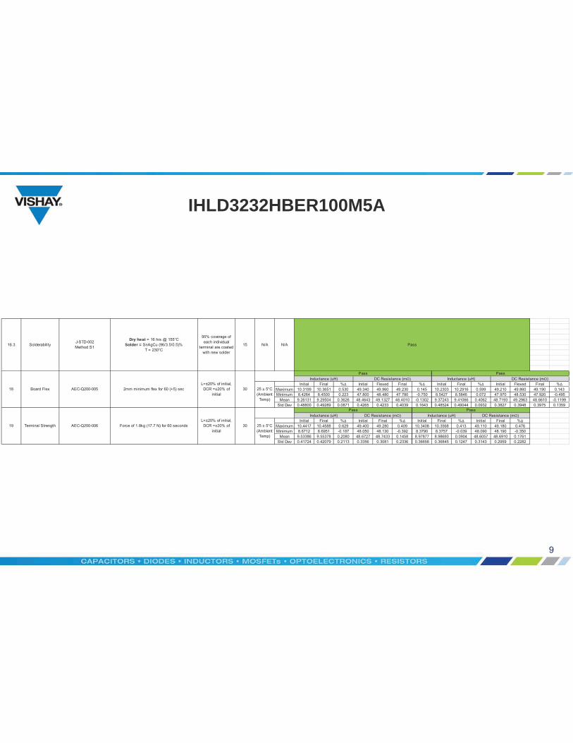
Board Flex AEC-Q200-005 2mm minimum flex for 60 (+5) secL=±20% of initial, DCR =±20% of
initial30
Pass PassInductance (uH) DC Resistance (m ) Inductance (uH) DC Resistance (m )
25 ± 5°C(Ambient
Temp)
19 Terminal Strength AEC-Q200-006 Force of 1.8kg (17.7 N) for 60 secondsL=±20% of initial, DCR =±20% of
initial30 25 ± 5°C
(AmbientTemp)
18
Pass PassInductance (uH) DC Resistance (m ) Inductance (uH) DC Resistance (m )
N/A N/A Pass16.3 SolderabilityJ-STD-002Method S1
Dry heat = 16 hrs @ 155°CSolder = SnAgCu (96/3.5/0.5)%
T = 230°C
95% coverage of each individual
terminal are coated with new solder
15

Production Part Approval ProcessThe following PPAP documentation is assembled according to
AIAG, 4th Edition PPAP Manual and applicable customer requirements
Initial Process StudyIHLD3232HBER100M5A, Inductance L1-2
464136312621161161
10.0
9.5
9.0
Indi
vidu
al V
alue
_X=9.628
UCL=10.243
LCL=9.012
464136312621161161
0.8
0.4
0.0
Mov
ing
Rang
e
__MR=0.2314
UCL=0.7561
LCL=0
5045403530
10.0
9.6
9.2
Observation
Val
ues
12.011.410.810.29.69.08.4
LSL 8USL 12
Specifications
LSL USL
OverallWithin
10.09.59.0
StDev 0.2052Cp 3.25Cpk 2.64PPM 0.00
WithinStDev 0.2342Pp 2.85Ppk 2.32Cpm *PPM 0.00
OverallOverall
Within
Specs
Initial Process Study, IHLD3232HBER100M5A, Inductance L1-2I Chart
Moving Range Chart
Last 25 Observations
Capability Histogram
Normal Prob PlotAD: 0.775, P: 0.041
Capability Plot
1 9.725 26 9.4352 9.258 27 9.5063 9.165 28 9.7744 9.282 29 9.2645 9.291 30 9.6476 9.908 31 9.5127 9.752 32 9.9478 9.859 33 9.5169 9.855 34 9.51610 9.723 35 9.94411 9.886 36 9.97612 9.255 37 9.41513 9.613 38 9.97514 9.555 39 9.52715 9.451 40 9.67916 9.982 41 9.54417 9.767 42 9.71218 9.538 43 9.92119 9.519 44 9.61520 9.923 45 9.68521 9.891 46 9.32622 9.901 47 9.25523 9.949 48 9.57624 9.551 49 9.42225 9.552 50 9.535
Inductance (uH)

Production Part Approval ProcessThe following PPAP documentation is assembled according to
AIAG, 4th Edition PPAP Manual and applicable customer requirements
Initial Process StudyIHLD3232HBER100M5A, Inductance L3-4
464136312621161161
10.0
9.5
9.0
Indi
vidu
al V
alue
_X=9.678
UCL=10.350
LCL=9.006
464136312621161161
0.8
0.4
0.0
Mov
ing
Rang
e
__MR=0.2528
UCL=0.8260
LCL=0
5045403530
10.0
9.6
9.2
Observation
Val
ues
12.011.410.810.29.69.08.4
LSL 8USL 12
Specifications
LSL USL
OverallWithin
10.510.09.59.0
StDev 0.2241Cp 2.97Cpk 2.50PPM 0.00
WithinStDev 0.2686Pp 2.48Ppk 2.08Cpm *PPM 0.00
OverallOverall
Within
Specs
Initial Process Study, IHLD3232HBER100M5A, Inductance L3-4I Chart
Moving Range Chart
Last 25 Observations
Capability Histogram
Normal Prob PlotAD: 1.075, P: 0.007
Capability Plot
1 9.957 26 9.9042 9.41 27 9.6113 9.212 28 9.6444 9.413 29 9.8415 9.865 30 9.4066 9.767 31 10.1057 9.282 32 9.5618 9.21 33 9.2129 9.409 34 9.88210 9.209 35 9.56611 9.888 36 9.43312 9.814 37 9.84413 9.913 38 9.81514 9.968 39 10.08315 9.417 40 10.06216 9.335 41 9.98917 9.615 42 9.62718 9.225 43 9.72119 9.584 44 9.93320 9.652 45 9.96121 9.28 46 9.87822 9.869 47 9.88423 10.05 48 9.61424 9.831 49 9.75225 9.847 50 9.552
Inductance (uH)

Production Part Approval ProcessThe following PPAP documentation is assembled according to
AIAG, 4th Edition PPAP Manual and applicable customer requirements
Initial Process StudyIHLD3232HBER100M5A, DC Resistance L1-2
464136312621161161
49.6
49.2
48.8
Indi
vidu
al V
alue
_X=49.2332
UCL=49.6698
LCL=48.7966
464136312621161161
0.4
0.2
0.0
Mov
ing
Rang
e
__MR=0.1642
UCL=0.5364
LCL=0
5045403530
49.4
49.2
49.0
Observation
Val
ues
53.452.852.251.651.050.449.849.2
USL 53.5Specifications
USL
OverallWithin
49.849.549.248.9
StDev 0.1455Cp *Cpk 9.77PPM 0.00
WithinStDev 0.1544Pp *Ppk 9.21Cpm *PPM 0.00
OverallOverall
Within
Specs
Initial Process Study, IHLD3232HBER100M5A, DCR L1-2I Chart
Moving Range Chart
Last 25 Observations
Capability Histogram
Normal Prob PlotAD: 0.317, P: 0.529
Capability Plot
1 49.39 26 48.962 49.3 27 49.233 49.4 28 49.134 49.21 29 49.325 49.59 30 49.336 49.39 31 49.297 49.43 32 49.138 49.21 33 48.959 49.4 34 48.9710 49.24 35 49.1311 48.91 36 49.312 49.02 37 49.1213 49.15 38 49.3414 49.25 39 49.1115 49.39 40 48.9816 49.31 41 49.2917 49.49 42 49.3418 49.13 43 49.1919 49.52 44 49.0320 49.35 45 49.2121 49.27 46 49.1422 49.118 47 49.2723 49.32 48 49.4124 49.19 49 49.1225 49.26 50 49.13
DCR (mOhm)

Production Part Approval ProcessThe following PPAP documentation is assembled according to
AIAG, 4th Edition PPAP Manual and applicable customer requirements
Initial Process StudyIHLD3232HBER100M5A, DC Resistance L3-4
464136312621161161
49.6
49.2
48.8
Indi
vidu
al V
alue
_X=49.2094
UCL=49.6405
LCL=48.7782
464136312621161161
0.4
0.2
0.0
Mov
ing
Rang
e
__MR=0.1621
UCL=0.5297
LCL=0
5045403530
49.50
49.25
49.00
Observation
Val
ues
53.452.852.251.651.050.449.849.2
USL 53.5Specifications
USL
OverallWithin
49.649.248.8
StDev 0.1437Cp *Cpk 9.95PPM 0.00
WithinStDev 0.1564Pp *Ppk 9.15Cpm *PPM 0.00
OverallOverall
Within
Specs
Initial Process Study, IHLD3232HBER100M5A, DCR L3-4I Chart
Moving Range Chart
Last 25 Observations
Capability Histogram
Normal Prob PlotAD: 0.696, P: 0.065
Capability Plot
1 49.13 26 49.282 49.52 27 49.33 49.35 28 49.44 49.27 29 49.215 49.118 30 49.596 49.32 31 49.397 49.19 32 49.438 49.26 33 49.219 48.96 34 49.410 49.23 35 49.2411 49.13 36 48.9112 49.32 37 49.0213 49.33 38 49.1514 49.29 39 49.2515 49.13 40 49.2916 48.95 41 49.1317 48.97 42 48.9518 49.13 43 48.9719 49.3 44 49.1320 49.12 45 49.321 49.34 46 49.1222 49.11 47 49.3423 48.98 48 49.1124 49.29 49 48.9825 49.34 50 49.29
DCR (mOhm)

Production Part Approval ProcessThe following PPAP documentation is assembled according to
AIAG, 4th Edition PPAP Manual and applicable customer requirements
Use the control buttons below to navigate through the PPAP sections.
Section 12: Qualified Laboratories
Page 89

Production Part Approval ProcessThe following PPAP documentation is assembled according to
AIAG, 4th Edition PPAP Manual and applicable customer requirements
Page 81
Production Part Approval ProcessThe following PPAP documentation is assembled according to
AIAG, 4th Edition PPAP Manual and applicable customer requirements
Page 82

Production Part Approval ProcessThe following PPAP documentation is assembled according to
AIAG, 4th Edition PPAP Manual and applicable customer requirements
Page 83

Production Part Approval ProcessThe following PPAP documentation is assembled according to
AIAG, 4th Edition PPAP Manual and applicable customer requirements
Page 84

Production Part Approval ProcessThe following PPAP documentation is assembled according to
AIAG, 4th Edition PPAP Manual and applicable customer requirements
Use the control buttons below to navigate through the PPAP sections.
Section 17: Records of Compliance
Page 99

Production Part Approval ProcessThe following PPAP documentation is assembled according to
AIAG, 4th Edition PPAP Manual and applicable customer requirements
Page 91

V I S H A Y D A L E
Magnetics Application Note
IHLP Standards of Manufacture
AP
PL
ICA
TIO
N N
OT
E
Revision: 30-Apr-13 1 Document Number: 34352
For technical questions, contact: [email protected] DOCUMENT IS SUBJECT TO CHANGE WITHOUT NOTICE. THE PRODUCTS DESCRIBED HEREIN AND THIS DOCUMENT
ARE SUBJECT TO SPECIFIC DISCLAIMERS, SET FORTH AT www.vishay.com/doc?91000
www.vishay.com
IHLP INTRODUCTION SURFACE IRREGULARITIES CRITERIA FOR REJECTION SUMMARY
INTRODUCTION
Scope
This document was written for the purpose of helping customers better understand the product they are purchasing. It will give the customer an idea as to the type of cosmetic irregularities that may occur from time to time during the manufacture of the component itself or during customer use of the component.
This document also discusses the criteria that have been developed for rejection of irregularities that are determined to be excessive.
While it would be desirable to have cosmetically perfect IHLP inductors, the powdered iron manufacturing technique has cosmetic limitations.
Certified test labs have performed extensive environmental testing on IHLP’s with and without cosmetic imperfections according to AEC-Q200 standards for such tests as thermal shock, mechanical shock, vibration, humidity and others. This testing has shown that the cosmetic imperfections listed in this document do not affect the performance or reliability of the IHLP inductor. Test results are available upon request.
Product
The IHLP inductor is unique from most inductors. The inductor body is a soft magnetic composite (SMC), not a ferrite. It is made from an iron powder mixture and cemented together using a resin binder. This powder mixture, when pressed around the inductor coil, greatly enhances the electrical properties of the inductor and gives protection from environmental forces. After pressing, the component is cured in an oven to increase the bonding strength of the resin binders with the iron powder, yielding excellent electrical and physical properties.
The IHLP inductor provides the best combination of:
• Inductance• Low Core Loss• Saturation• Temperature Stability• Smallest Footprint• Lowest Profile
Surface irregularities
The following pages include descriptions of the most common irregularities seen on IHLP inductors. Common causes are described along with variations in their magnitude. Customers may at some time see one or all of these irregularities.
Those that are determined to adversely affect the customer’s use of the component are rejected, but minor (acceptable) irregularities will occasionally be present. With the use of this guide, a customer will better understand the effect of each irregularity.
Cracks
Chips
Oxidation
IHLP Standards of Manufacture
AP
PL
ICA
TIO
N N
OT
EApplication Note
www.vishay.com Vishay Dale
Revision: 30-Apr-13 2 Document Number: 34352
For technical questions, contact: [email protected] DOCUMENT IS SUBJECT TO CHANGE WITHOUT NOTICE. THE PRODUCTS DESCRIBED HEREIN AND THIS DOCUMENT
ARE SUBJECT TO SPECIFIC DISCLAIMERS, SET FORTH AT www.vishay.com/doc?91000
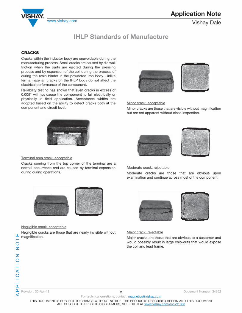
CRACKSCracks within the inductor body are unavoidable during the manufacturing process. Small cracks are caused by die wall friction when the parts are ejected during the pressing process and by expansion of the coil during the process of curing the resin binder in the powdered iron body. Unlike ferrite material, cracks on the IHLP body do not affect the electrical performance of the component.
Reliability testing has shown that even cracks in excess of 0.005" will not cause the component to fail electrically or physically in field application. Acceptance widths are adopted based on the ability to detect cracks both at the component and circuit level.
Terminal area crack, acceptable
Cracks coming from the top corner of the terminal are a normal occurrence and are caused by terminal expansion during curing operations.
Negligible crack, acceptable
Negligible cracks are those that are nearly invisible without magnification.
Minor crack, acceptable
Minor cracks are those that are visible without magnification but are not apparent without close inspection.
Moderate crack, rejectable
Moderate cracks are those that are obvious upon examination and continue across most of the component.
Major crack, rejectable
Major cracks are those that are obvious to a customer and would possibly result in large chip-outs that would expose the coil and lead frame.

IHLP Standards of Manufacture
AP
PL
ICA
TIO
N N
OT
EApplication Note
www.vishay.com Vishay Dale
Revision: 30-Apr-13 3 Document Number: 34352
For technical questions, contact: [email protected] DOCUMENT IS SUBJECT TO CHANGE WITHOUT NOTICE. THE PRODUCTS DESCRIBED HEREIN AND THIS DOCUMENT
ARE SUBJECT TO SPECIFIC DISCLAIMERS, SET FORTH AT www.vishay.com/doc?91000
CHIPSChipping of the inductor body can occur during normal processing and testing of the inductor. The acceptance criteria for chipping vary with the size of the component, but current acceptance standards are based on IPCA-610. The effect of chipping is negligible as long as the inductor coil is not showing. See IPC standard for class 1 and 2 components below.
Chips typically occur on the edges and corners of the inductor body. They are slightly darker in color and rougher in appearance than the surrounding material.
Minor chipping, acceptable
Minor chips in the inductor body are those that are typically shallow imperfections that occur on the corners and edge of components. No coil wire or lead frame is showing and the chip does not affect the performance or reliability of the component.
Major chipping, rejectable
Major chips in the inductor body are those that are very obvious to the customer and may expose the wire coil or lead frame.
OXIDATIONThe IHLP inductor is predominately iron and oxidation may occur in a small percentage of the inductors. Resin binders give moderate protection, but some slight oxidation may occur. All components should be stored away from heat, humidity and ionized atmospheres as much as possible before mounting.
Basic steps should be taken in order to limit surface oxidation, including keeping the IHLP inductors sealed in their packaging until PCB mounting.
In the case that oxidation does occur, the effects are contained to the surface of the component and do not penetrate into the core material. No electrical effects have ever been documented due to oxidation of the IHLP product. Oxidation should never be considered a reliability risk.
Top view
Side view
T 25 % of the thickness
W 25 % of the width
L 50 % of the length

IHLP Standards of Manufacture
AP
PL
ICA
TIO
N N
OT
EApplication Note
www.vishay.com Vishay Dale
Revision: 30-Apr-13 4 Document Number: 34352
For technical questions, contact: [email protected] DOCUMENT IS SUBJECT TO CHANGE WITHOUT NOTICE. THE PRODUCTS DESCRIBED HEREIN AND THIS DOCUMENT
ARE SUBJECT TO SPECIFIC DISCLAIMERS, SET FORTH AT www.vishay.com/doc?91000
OTHERA very small number of other irregularities have been reported. These occur at an exceedingly low rate and typically do not affect the components electrically. These include:
Foreign material may be seen pressed into the upper terminals. This material is of the same material as the inductor body and should not be a reason for rejection unless solderability is affected.
Foreign material: Acceptable
Scratches may be seen on the surface of the inductor body. Scratches are an acceptable surface irregularity.
Scratch: Acceptable
SUMMARYThe IHLP inductor is comprised of an iron powder body compressed around a coil. Due to the fact that this iron powder body is not solid like ferrite material, irregularities such as cracks and chips do not affect the electrical properties, or the reliability of the component. Criteria have been determined for the acceptability of the components that allow for a robust manufacturing process as well as an acceptable degree of cosmetic irregularity.
Reliability testing has been done on the effects of cracking of the iron powder body and on the oxidation of the iron particles that are present on the surface. Testing has shown no reliability issues from either of these cosmetic differences.
IHLP Solder Profile and Cleaning Guidewww.vishay.com Vishay Dale
Revision: 22-Jun-12 1 Document Number: 34339
For technical questions, contact: [email protected] DOCUMENT IS SUBJECT TO CHANGE WITHOUT NOTICE. THE PRODUCTS DESCRIBED HEREIN AND THIS DOCUMENT
ARE SUBJECT TO SPECIFIC DISCLAIMERS, SET FORTH AT www.vishay.com/doc?91000
Instructions
ASSEMBLY INSTRUCTIONS
General
This document provides instructions on mounting for thedifferent types of packages, specifically on the differentmethods of soldering.
If the device is to be mounted near heat-generatingcomponents, consideration must be given to the resultantincrease in ambient temperature.
Soldering Instructions
Protection against overheating is essential when a device isbeing soldered. Therefore, the PCB traces should be left aslong as possible. The maximum permissible solderingtemperature is governed by the maximum permissible heatthat may be applied to the package.
The maximum soldering iron (or solder bath) temperaturesare given in the individual Datasheets. During soldering, noforces must be transmitted from the pins to the case (e.g.,by spreading the pins).
Soldering Methods
There are several methods for soldering devices onto thesubstrate. The following list is not complete.
a. Soldering in the Vapor PhaseSoldering in saturated vapor is also known ascondensation soldering. This soldering process is usedas a batch system (dual vapor system) or as a continuoussingle vapor system. Both systems may also include apre-heating of the assemblies to prevent hightemperature shock and other undesired effects.
b. Infrared SolderingBy using infrared (IR) reflow soldering, the heating iscontact-free and the energy for heating the assembly isderived from direct infrared radiation and fromconvection.
The heating rate in an IR furnace depends on theabsorption coefficients of the material surfaces and onthe ratio of component's mass to an As-irradiatedsurface.
The temperature of parts in an IR furnace, with a mixtureof radiation and convection, cannot be determined inadvance. Temperature measurement may be performedby measuring the temperature of a certain componentwhile it is being transported through the furnace.
The temperatures of small components, solderedtogether with larger ones, may rise up to 280 °C.
Influencing parameters on the internal temperature of thecomponent are as follows:
• Time and power
• Mass of the component
• Size of the component
• Size of the printed circuit board
• Absorption coefficient of the surfaces
• Packing density
• Wavelength spectrum of the radiation source
• Ratio of radiated and convected energy
As a general rule of thumb, maximum temperatureshould be reached within 360 s and time above solderliquids temperature should be reached in less than 180 s.
Temperature/time profiles of the entire process and theinfluencing parameters are given. The IR reflow profile isshown in Figure 1.
c. Wave SolderingIn wave soldering one or more continuously replenishedwaves of molten solder are generated, while thesubstrates to be soldered are moved in one directionacross the crest of the wave. Maximum solderingtemperature should not exceed 260 °C for 20 s.
d. Iron SolderingThis process cannot be carried out in a controlledsituation. It should therefore not be used in applicationswhere reliability is important. There is no SMDclassification for this process.
CLEANING INSTRUCTIONSA no clean solder system is recommended for IHLP’s.If cleaning must be performed, an Isopropyl alcohol is recommended. If de-ionized Water Wash is used insure it is followed bya thorough warm air dry cycle to avoid oxidation.
Some cleaning solutions, especially those containing non-linear alcohol will attack the IHLP and should be avoided. It isrecommended that any chemical cleaning solution be thoroughly rinsed with clean water. The IHLP should be tested forcompatibility with any cleaning solution before production assembly.

IHLP Solder Profile and Cleaning Guidewww.vishay.com Vishay Dale
Revision: 22-Jun-12 2 Document Number: 34339
For technical questions, contact: [email protected] DOCUMENT IS SUBJECT TO CHANGE WITHOUT NOTICE. THE PRODUCTS DESCRIBED HEREIN AND THIS DOCUMENT
ARE SUBJECT TO SPECIFIC DISCLAIMERS, SET FORTH AT www.vishay.com/doc?91000
TYPICAL REFLOW SOLDERING PROFILE
Fig. 1 - Infrared reflow soldering (SMD package)
LEAD (Pb)-FREE SOLDER (SnAgCu) REFLOW PROFILE ATTRIBUTESPROFILE ATTRIBUTE PROFILE ATTRIBUTE
Peak Reflow Temperature 255 (± 5) °C
Time within 5 °C of Peak Temperature 30 s max.
Liquidus Temperature of Solder ~ 217 °C
Cool Down Rate 6 °C/s max.
Time above Liquidus 60 s to 150 s
Pre-heat Temperature Range 150 °C to 200 °C
Pre-heat Dwell Time 60 s to 120 s
Maximum Ramp Rate 3 °C/s max.
Liquidus Temperature of Solder
Peak Reflow Temperature
Tem
per
atu
re
Time
Duration within 5 °C of Peak Temp
Time Above Liquidus
Ramp Rate
Pre-Heat Dwell Time
Pre-Heat Temp RangeCool Down Rate
Recommended