Scholars' Mine Scholars' Mine
Masters Theses Student Theses and Dissertations
Fall 2007
Printed circuit board (PCB) loss characterization up-to 20 GHz Printed circuit board (PCB) loss characterization up-to 20 GHz
and modeling, analysis and validation and modeling, analysis and validation
Abhilash Rajagopal
Follow this and additional works at: https://scholarsmine.mst.edu/masters_theses
Part of the Computer Engineering Commons
Department: Department:
Recommended Citation Recommended Citation Rajagopal, Abhilash, "Printed circuit board (PCB) loss characterization up-to 20 GHz and modeling, analysis and validation" (2007). Masters Theses. 4570. https://scholarsmine.mst.edu/masters_theses/4570
This thesis is brought to you by Scholars' Mine, a service of the Missouri S&T Library and Learning Resources. This work is protected by U. S. Copyright Law. Unauthorized use including reproduction for redistribution requires the permission of the copyright holder. For more information, please contact [email protected].
0
PRINTED CIRCUIT BOARD (PCB) LOSS CHARACTERIZATION UP-TO 20 GHz
AND
MODELING, ANALYSIS AND VALIDATION
by
ABHILASH RAJAGOPAL
A THESIS
Presented to the Faculty of the Graduate School of the
UNIVERSITY OF MISSOURI-ROLLA
In Partial Fulfillment of the Requirements for the Degree
MASTER OF SCIENCE IN COMPUTER ENGINEERING
2007
_______________________________ _______________________________ James L. Drewniak, Advisor Daryl. G. Beetner
_______________________________ Richard. E. DuBroff

1
© 2007
Abhilash Rajagopal
All Rights Reserved
iii
ABSTRACT
Dielectric properties and losses are increasingly more important in signal link
path characterization, as data rates increases. High-frequency effects such as dielectric
losses, dispersion and skin-effect losses need to be considered. For ensuring signal
integrity, it is important to characterize losses of printed circuit board (PCB) dielectrics.
To extract dielectric properties of a stripline transmission medium, an analytical
technique was used as described in [1]. Two test materials were studied, and the
extraction procedure was refined. This technique was applied to microstrip transmission
lines. Two analytical solutions were derived for extracting practical material parameters.
A microstrip test vehicle was designed and the two extraction methods were applied to a
set of test boards. A standard measurement protocol was developed. Results were
analyzed and documented.
An approach to characterize losses in printed circuit board (PCB) materials as a
single value was studied. It was analytically proven that the theory was meaningful.
Time-domain and frequency-domain techniques were developed to characterize the
single value loss parameter. Measurements were taken with stripline test vehicles. Results
validated the method to be a potential standard for characterizing losses.
Several tools are available in the market for design and discovery related to signal
integrity issues. Some of these tools were considered to model two simple validation
problems. Propagation of a plane wave through a dielectric slab was analyzed with two
different tools and results were also validated using calculations. A simple PCB was
modeled with decoupling capacitors using several tools to see the effects of decoupling
on impedance.

iv
ACKNOWLEDGMENTS
I express my deep and sincere gratitude to Dr. James L. Drewniak for his constant
guidance and mentoring throughout the pursuit of my Master’s degree. I thank Dr.
Pommerenke for his support and enlightening discussions. I thank all my fellow students
of the UMR EMC laboratory who I have been working with during these years. I also
want to thank the committee members of my thesis defense, and I’m grateful for the
financial support of research assistantship from the UMR EMC Laboratory. Finally, I
would like to thank my family and dedicate this work to them, for their unconditional
love, support, and encouragement throughout my education and life.
v
TABLE OF CONTENTS
Page
ABSTRACT....................................................................................................................... iii
ACKNOWLEDGMENTS ................................................................................................. iv
LIST OF ILLUSTRATIONS............................................................................................ vii
LIST OF TABLES............................................................................................................. xi
SECTION
1. INTRODUCTION ...........................................................................................................1
1.1. PCB MATERIAL PARAMETER EXTRACTION................................................ 1
1.2. ROOT IMPULSE ENERGY (RIE) LOSS ............................................................. 2
1.3. ANALYSIS, MODELING AND VALIDATION.................................................. 3
2. PRINTED CIRCUIT BOARD (PCB) MATERIAL PARAMETER EXTRACTION UP TO 20 GHz...............................................................................................................5
2.1. EXTRACTION OF MATERIAL PARAMETERS FROM STRIPLINE .............. 9
2.1.1. Description of Geometry................................................................................... 9
2.1.2. Material Extraction Procedure for Stripline.................................................... 11
2.1.3. Test Setup, Calibration and Measurements .................................................... 14
2.1.4. Extracted Results and Analysis....................................................................... 22
2.2. EXTRACTION OF MATERIAL PARAMETERS FROM MICROSTRIP ........ 25
2.2.1. Geometry and Test Vehicle Design ................................................................ 25
2.2.2. Material Extraction Procedure for Microstrip................................................. 36
2.2.2.1. Approximation method .......................................................................... 36
2.2.2.2. Curve-fitting method.............................................................................. 39
2.2.2.3. Comparison of two methods .................................................................. 40
2.2.3. Test Setup, Settings and Measurements.......................................................... 41
2.2.4. Measurements and Analysis ........................................................................... 46
2.2.5. Comparison and Analysis. .............................................................................. 51
2.2.6. Extracted Results ............................................................................................ 57
3. ROOT IMPULSE ENERGY (RIE) LOSS ....................................................................60
3.1. TIME DOMAIN CHARACTERIZATION.......................................................... 61
3.2. FRQUENCY DOMAIN CHARACTERIZATION .............................................. 63

vi
3.3. ANALYTICAL EXPRESSION ANALYSIS OF RIE LOSS FOR STRIPLINE. 64
3.3.1. Description of the Geometry and Losses ........................................................ 65
3.3.2. Attenuation Due to Dielectric Loss (αd) ......................................................... 67
3.3.3. Attenuation Due to Conductor Loss (αc) ........................................................ 67
3.3.4. Losses in Terms of Frequency for the Selected Stripline Structure................ 68
3.3.5. Derivation of Analytical Expression for RIE Loss ......................................... 69
3.4. MEASUREMENTS AND RESULTS.................................................................. 74
3.4.1. Frequency Domain Measurements ................................................................. 74
3.4.2. Time Domain Measurements.......................................................................... 75
3.4.3. RIE Loss Comparison and Analysis ............................................................... 78
4. ANALYSIS, MODELING AND VALIDATION.........................................................82
4.1. PROPAGATION DELAY THROUGH A DIELECTRIC SLAB........................ 83
4.1.1. Geometry Description..................................................................................... 83
4.1.2. Time Delay Calculation .................................................................................. 83
4.1.3. Modeling Geometry using EZ-FDTD............................................................. 84
4.1.4. Simulation and Analysis using EZ-FDTD...................................................... 86
4.1.5. Modeling and Simulation using PSPICE........................................................ 92
4.1.6. Comparison and Validation ............................................................................ 94
4.2. DECOUPLING POWER/GROUND PLANES IN PCBs .................................... 96
4.2.1. Geometry Description..................................................................................... 97
4.2.2. Modeling using Cavity Resonance Tool (EZPP)............................................ 98
4.2.3. Modeling using Full Wave Tool (EZFDTD) ................................................ 100
4.2.4. Modeling using Full Wave Tool (Microwave Studio).................................. 102
4.2.5. Results and Comparison ............................................................................... 104
5. SUMMARY.................................................................................................................111
BIBLIOGRAPHY............................................................................................................112
VITA................................................................................................................................114

vii
LIST OF ILLUSTRATIONS Figure Page
2.1. Channel performance degradation in several cases due to length dependent losses in transmission lines .........................................................................................6
2.2. General flow diagram for generating a new material parameter matrix.................... 8
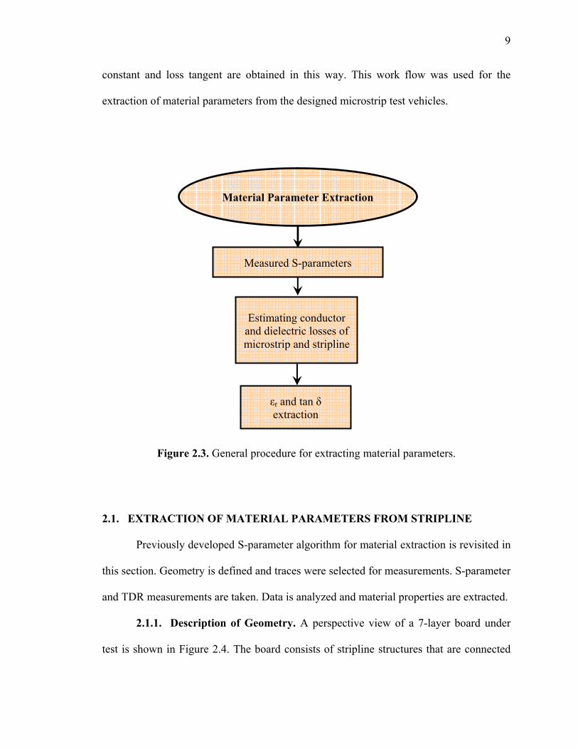
2.3. General procedure for extracting material parameters............................................... 9
2.4. Perspective view of the stripline test board ............................................................. 10
2.5. Layout of a base structure with TRL cal patterns and test traces ............................ 11
2.6. Stack up of a single stripline structure (all dimensions are in mils) ........................ 12
2.7. Material extraction procedure for stripline .............................................................. 14
2.8. Test setup used for stripline measurements ............................................................. 16
2.9. VNA measurement results for “Thru” standard .......................................................17
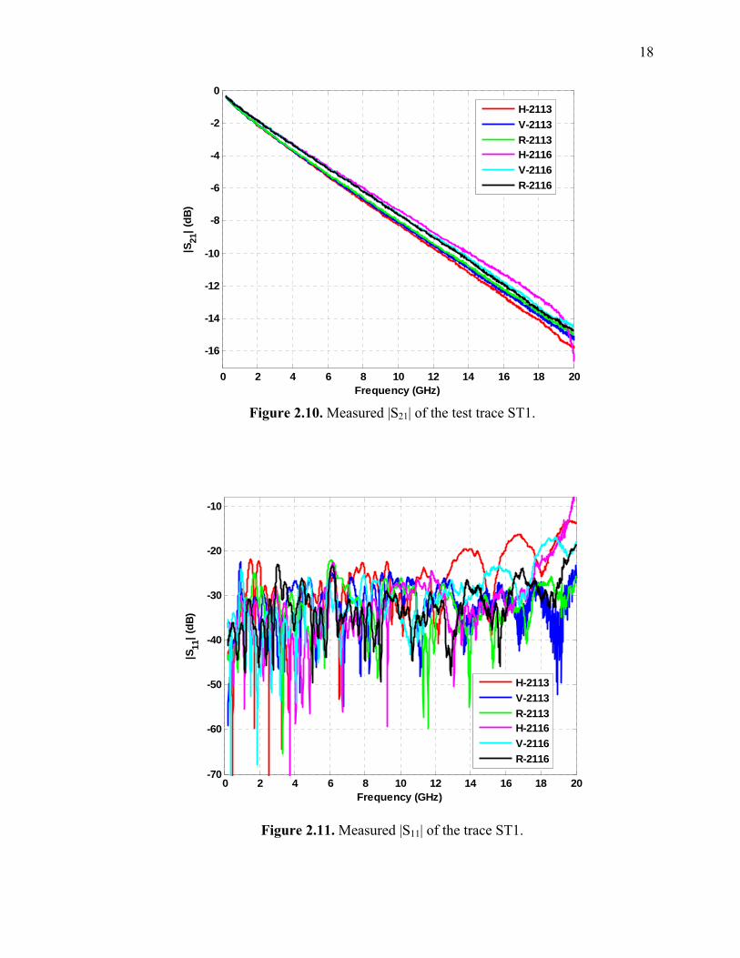
2.10. Measured |S21| of the test trace ST1 ......................................................................... 18
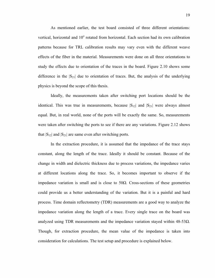
2.11. Measured |S11| of the trace ST1................................................................................ 18
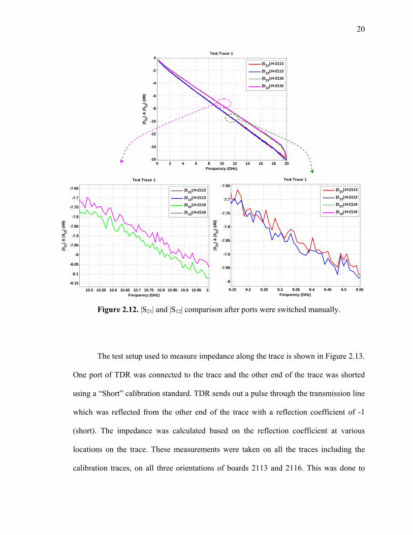
2.12. |S21| and |S12| comparison after ports were switched manually................................ 20
2.13. Test setup used to measure impedance along the length of a trace ......................... 21
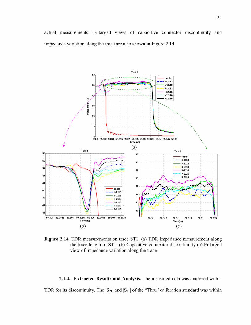
2.14. TDR measurements on trace ST1 .............................................................................22
2.15. Dielectric constant, as a function of frequency for Board 2113 and Board 2116.... 24
2.16. Loss tangent, as a function of frequency for Board 2113 and Board 2116 ............. 24
2.17. Microstrip geometry ................................................................................................ 26
2.18. Loss curves obtained after using the current geometry parameters with the cross over point at 0.6 GHz................................................................................................28
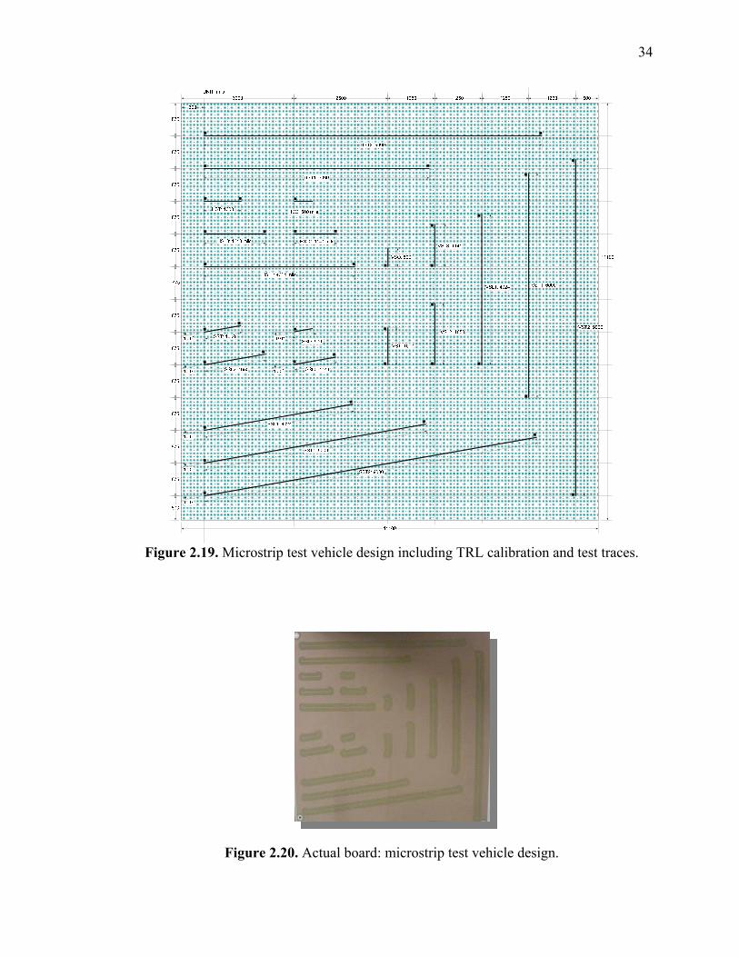
2.19. Microstrip test vehicle design including TRL calibration and test traces................ 34
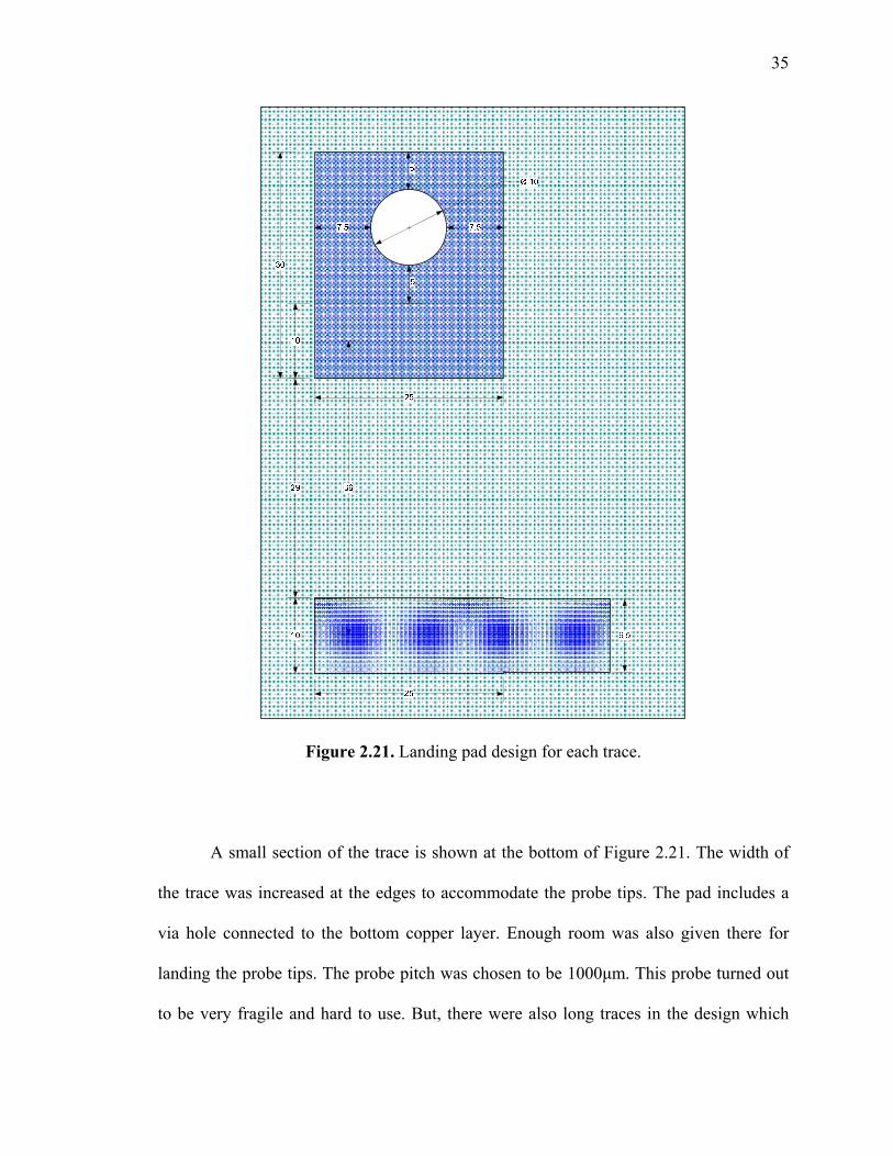
2.20. Actual board: microstrip test vehicle design............................................................ 34

viii
2.21. Landing pad design for each trace ........................................................................... 35
2.22. Material extraction algorithm (approximation technique) for microstrip................ 37
2.23. Material extraction procedure (curve-fitting) for microstrip ................................... 40
2.24. Extraction method comparison .................................................................................41
2.25. Test setup for microstrip test board measurement ................................................... 42
2.26. View of pads configuration and probe configuration at the edge of traces on the test boards .................................................................................................................44
2.27. TDR measurements on the traces showing the large inductance on both sides of the trace associated with the tips...............................................................................45
2.28. VNA measurements on microstrip board ................................................................ 46
2.29. Return loss for “Thru” standard, VST1 and VST2 .................................................. 47
2.30. |S21| of trace VST2 for all TRL calibrated samples ................................................. 48
2.31. |S11| of trace VST2 for all TRL calibrated samples ................................................. 48
2.32. Test setup used for TDR measurements on microstrip test boards.......................... 49
2.33. Impedance measurements on microstrip board ........................................................50
2.34. |S21| measurement comparison before and after cleaning the trace surface. ............ 51
2.35. TDR measurements after manual switching of ports and also the comparison before and after cleaning the trace surface ...............................................................54
2.36. Surface roughness measurement using Profilometer. .............................................. 54
2.37. Geometry of “Open” standard ................................................................................. 55
2.38. Comparison of |S21| with and without via in the “Open” standard .......................... 56
2.39. Measurement comparison for five samples of same material...................................57
2.40. Comparison of dielectric constant for all the samples tested................................... 58
2.41. Comparison of loss tangent for all the samples tested............................................. 59
3.1. S-parameter block of a two port network ................................................................ 63
ix
3.2. Stripline geometry chosen for RIE loss calculations ............................................... 65
3.3. Loss curves plotted from loss equation for the stripline test board ......................... 70
3.4. S-parameter measurements taken after doing TRL calibration ............................... 75
3.5. Test setup used to measure step response of the reflected wave ............................. 76
3.6. Measured TDR step response after reflection.......................................................... 77
3.7. Impulse response obtained by differentiating the measured TDR step response .... 78
3.8. RIE loss number calculated analytically as a function of loss tangent .................... 80
4.1. Gaussian wave propagating through a dielectric slab.............................................. 84
4.2. Cell domain for EZFDTD simulation with three monitor probes at different locations before and after the dielectric slab ............................................................85
4.3. Location of monitor probes and wave behavior at boundaries ................................ 87
4.4. Calculated and observed time along the wave propagation..................................... 90
4.5. Propagation delay through the slab with dielectric constant 2.5 ............................. 91
4.6. Propagation delay through the slab with dielectric constant 5 ................................ 91
4.7. Propagation delay through the slab with dielectric constant 10 .............................. 92
4.8. Circuit diagram in PSpice for εr = 2.5 ...................................................................... 93
4.9. The dielectric slab simulated in PSpice for εr = 2.5 ................................................. 93
4.10. Comparison of EZFDTD data with PSpice simulated data for εr = 2.5 ................... 94
4.11. Comparison of EZFDTD data with PSpice simulated data for εr = 5.0 ................... 95
4.12. Comparison of EZFDTD data with PSpice simulated data for εr = 10.0 ................. 96
4.13. Geometry information for decoupling on a printed circuit board (PCB)................. 98
4.14. Screenshot of EZPP tool with 95 capacitor case ..................................................... 98
4.15. EZPP parameter setup...............................................................................................99
4.16. Geometry defined in EZ-FDTD............................................................................. 101
x
4.17. Geometry modeled in CST .................................................................................... 102
4.18. Modeling parameters in CST................................................................................. 103
4.19. Transfer impedance from source to Output 1 for the board with no capacitors .... 104
4.20. Transfer impedance from source to Output 2 for the board with no capacitors .... 105
4.21. Transfer impedance from source to Output 3 for the board with no capacitors .... 105
4.22. Transfer impedance from source to Output 1 for the board with four capacitors (0.01μF) around the source.....................................................................................106
4.23. Transfer impedance from source to Output 1 for the board with four capacitors (0.1μF) around the source.......................................................................................107
4.24. Transfer impedance from source to Output 1 for the board with four capacitors (100pF) around the source ......................................................................................107
4.25. Transfer impedance from source to Output 1 for the board with 95 capacitors (0.01μF) around the source.....................................................................................108
4.26. Transfer impedance from source to Output 1 for the board with 95 capacitors (0.1μF) around the source.......................................................................................109
4.27. Transfer impedance from source to Output 1 for the board with 95 capacitors (100pF) around the source ......................................................................................109

xi
LIST OF TABLES
Table Page
2.1. TRL calibration lengths and other trace lengths for patterns on the PCB ............... 15
2.2. Frequency limitations for the microstrip test vehicle design ................................... 29
2.3. Parameters of single-ended microstrip TRL calibration kit..................................... 33
2.4. HIROX measurements for width variation along a trace......................................... 52
2.5. Profilometer measurements for surface roughness along a trace............................. 55
3.1. Geometry parameters used for the stripline test board ............................................ 65
3.2. Length of traces used in the stripline test board ...................................................... 74
3.3. RIE loss results and comparison.............................................................................. 79
3.4. Percentage difference of RIE loss between VNA and TDR methods ..................... 79
3.5. Projected value of loss tangent from RIE loss curves.............................................. 81
4.1. Comparison between calculations and tools of values at wave peaks ..................... 95
1
1. INTRODUCTION
Digital systems require signals to be transmitted from drivers to receivers. Signal
propagates through several discontinuities like connectors, transitions, lossy transmission
lines etc. along its path to the receiver. These discontinuities degrade the signal quality
and may even distort the original signal. So, the receiver may miss a bit if it does not fall
on a certain threshold level. Noise could also couple into the system from external
sources and degrade the signal. Some problems of this sort are solved using parity
checking. But, they are not practical in terms of cost and performance. Data rates are
going higher in modern digital systems and the requirement to achieve sufficient signal
integrity is increasing. Sufficient power integrity should also be maintained for proper
functioning of the device.
1.1. PCB MATERIAL PARAMETER EXTRACTION
Signals propagating in modern digital systems are getting progressively faster.
Traces on printed circuit boards which transmit signals from source to destination no
longer behave as simple conductors. As the data rates are going higher, these conductors
exhibit high frequency effects and have to be considered as transmission lines. Hence, it
becomes necessary to deal with high frequency effects such as skin effect loss, dielectric
loss, as well as dispersion. It is not just the conductor which exhibits loss, but as
frequency goes higher the dielectric used between the conductors also play an important
role. The timing issues relating to transmission lines are also becoming important in
today’s high speed digital designs. Hence, it becomes important to characterize the
materials for efficient signal integrity analysis.
2
Conventional single valued representation of dielectric constant and loss tangent
are becoming invalid because they are dependant on frequency. Several simulation tools
take in the material properties as a single valued number. But, as frequencies go as high
as 20 GHz, single valued representation no longer holds true. So, frequency dependent
models for dielectric constant and loss tangent are necessary to represent the actual
properties of the material. Several techniques are available in the literature to extract
material parameters. Cavity resonance method, two-line measurement method, etc are
different techniques used to extract material properties from raw measurements. A
method for extracting dielectric constant and loss tangent as a function of frequency was
proposed [1] using TRL calibrated S-parameters for stripline structures. Two methods for
extracting material parameters for a microstrip structure are presented in this thesis. This
section of thesis starts off with analyzing two stripline structures and then recreates the
measurement procedure suggested by J. Ziang [1]. Measurements and results are also
discussed. A Microstrip test board with TRL calibration patterns was designed. Test
boards made of 32 different materials were measured, analyzed and extracted for material
study.
1.2. ROOT IMPULSE ENERGY (RIE) LOSS
A method for characterizing loss in time and frequency domain is presented in this
section. Several methods are available to extract losses in terms of frequency [2-6]. But,
it will be very useful to have a single valued number to specify losses in terms of limits.
Also, several frequency domain techniques could be used to characterize losses since
losses are functions of frequency. It would also be useful to have a time domain

3
technique to characterize losses so that measurements could be made using simple, less
costly instruments like TDR. This section of the thesis provides a novel technique to
characterize losses in time domain. Frequency domain characterization based on the same
concept is also done to validate time domain method.
RIE loss is a single valued energy loss used to represent losses in a transmission
line. A step signal is injected into a transmission line and energy is lost when the signal
propagates through the transmission line. Characteristics of losses in a transmission line
can be determined by comparing RIE of the injected wave to the RIE of the received
wave. For avoiding the effects of losses due to cables, connectors and transitions, a
calibration trace is also used to deal with unwanted energy loss. The received step signal
is converted into an impulse response to encompass the widest possible frequency range.
Then the area under the impulse response is integrated over time to get the energy
associated with each trace. The ratio of energies of test trace to calibration trace gives the
RIE loss. Measurements are results are also analyzed in this section.
1.3. ANALYSIS, MODELING AND VALIDATION
Several tools are available in the market for analyzing and modeling signal
integrity issues. This section deals with modeling two common geometries and validating
the results with different tools. The first section considers the propagation delay through a
dielectric slab. The velocity through a medium is inversely proportional to the square root
of the permeability of the material. So, as the permeability goes higher, velocity
decreases. An electromagnetic wave takes longer to pass through a medium with higher
permeability. This time delay and the reflections from the boundaries are calculated in
4
this section of the thesis. This geometry is then modeled in different tools to validate the
results.
Design of dc power distribution networks (PDN) on a printed circuit board (PCB)
plays a vital role in maintaining power integrity. Several techniques are available to
ensure that the PDN provides necessary charge to the devices in the PCB [14-17]. Yet,
the design presents an increasingly difficult challenge for digital circuits with active
devices. The sizes of the circuits are getting smaller with more devices added to the same
board. This makes the power consumption levels go high. More devices are switching
and they are getting current starved. For the proper functioning of the devices, it is
necessary to have sufficient charge when it is required. As switching speeds go higher, a
simple PDN might not be enough to supply enough charge for the devices. PDN have to
be designed carefully with sufficient decoupling capacitors to provide the charge in a
timely manner. The study of PDN design with emphasis on the value of the decoupling
capacitors used was analyzed in one among a series of papers on PDN design strategies
[14]. The location of the decoupling capacitors was analyzed in the second paper [15].
The third paper deals with importance of the planes and the choice of material parameters
[16]. Fourth, among the series of papers studies the sources of PDN noise [17].
The study presented on this thesis is analyzing the location and value of
capacitors on a PDN design. Several values of capacitors were used on different locations
to see its effect on the impedance. Increasing decoupling capacitors on the board
decreases the impedance. Reducing the PDN impedance would allow current to flow
freely into the IC device when needed. Several cases were modeled using three different
signal integrity analysis tools. Validation of the results is also presented in this section.
5
2. PRINTED CIRCUIT BOARD (PCB) MATERIAL PARAMETER EXTRACTION UP TO 20 GHz
The correct estimation of material properties is very critical when dealing with
signal link path characterization. As data rate increases, it is important to consider high
frequency effects such as skin effect and dielectric losses, as well as dispersion. For such
cases, dielectric constant and loss tangent become functions of frequency. These losses
could significantly degrade the signal quality and close the eye in an eye diagram.
Furthermore, losses increase as the length of the transmission line increases, and these
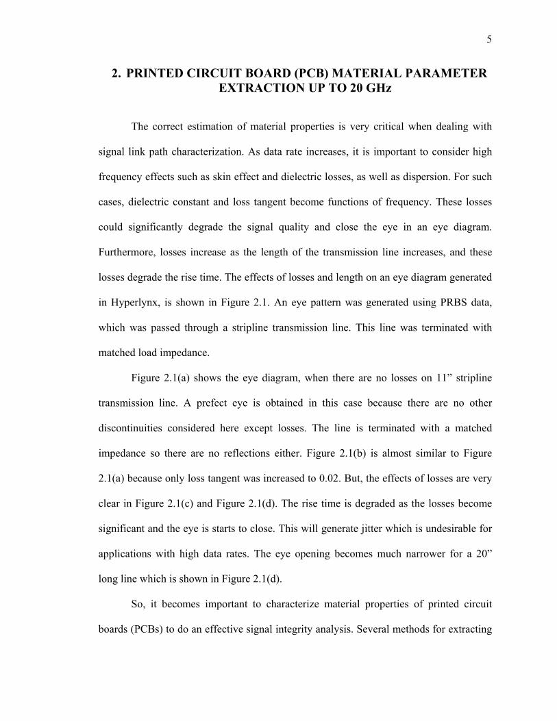
losses degrade the rise time. The effects of losses and length on an eye diagram generated
in Hyperlynx, is shown in Figure 2.1. An eye pattern was generated using PRBS data,
which was passed through a stripline transmission line. This line was terminated with
matched load impedance.
Figure 2.1(a) shows the eye diagram, when there are no losses on 11” stripline
transmission line. A prefect eye is obtained in this case because there are no other
discontinuities considered here except losses. The line is terminated with a matched
impedance so there are no reflections either. Figure 2.1(b) is almost similar to Figure
2.1(a) because only loss tangent was increased to 0.02. But, the effects of losses are very
clear in Figure 2.1(c) and Figure 2.1(d). The rise time is degraded as the losses become
significant and the eye is starts to close. This will generate jitter which is undesirable for
applications with high data rates. The eye opening becomes much narrower for a 20”
long line which is shown in Figure 2.1(d).
So, it becomes important to characterize material properties of printed circuit
boards (PCBs) to do an effective signal integrity analysis. Several methods for extracting
6
material properties are reported in the literature [1-6]. Each has its own advantage
depending on the material or the band of frequencies.
Figure 2.1. Channel performance degradation in several cases due to length dependent
losses in transmission lines. A resonant cavity technique is available for single or narrow band frequencies,
which provides dielectric parameters at higher frequencies with good accuracy [2]. A
coaxial technique is also available but the material has to be in powder form and it is hard
to use de-embedding techniques, which becomes critical at higher frequencies [4]. Direct
measurements can be done using impedance analyzer to obtain dielectric constant and
loss tangent, though it is limited to lower frequencies [6]. A method for the extraction of
(a) Length = 11”; tan δ = 0 (b) Length = 11”; tan δ = 0.02
(c) Length = 11”; tan δ = 0.2 (c) Length = 20”; tan δ = 0.2
7
material parameters such as dielectric constant and loss tangent as a function of
frequency based on measured S-parameters is also available [1], and is of interest to the
study in this Section. In this method [1], a stripline geometry was considered and
measurements were made only on a single FR-4 material.
There are several FR-4 materials available in the market from different vendors
and suppliers. They differ based on their resin content and different methodologies are
adopted by vendors to extract material properties. So, it becomes difficult for a board
designer to choose which material to use, and from where. Knowledge of the material
properties from a set of materials available in the market could help a designer choose
between materials for specific applications. Some high speed applications with long
traces require the use of low loss materials, and there are some applications where
sufficient loss is required for the proper functioning of devices. For example, for reducing
the power plane impedance for power integrity issues, increasing dielectric loss can be
beneficial. This Section deals with generating a parameter matrix of different materials
from different vendors using an S-parameter measurement technique [1]. To validate the
technique, two new materials of stripline construction were studied in the first section of
this Section and the procedure was refined. stripline structures were measured using
SMA connectors. This proved troublesome for high frequency measurements. Therefore,
a new, simple, two-layer microstrip test board was designed. The absence of additional
via stubs in the microstrip geometry also proved beneficial in designing a new microstrip
test board for the material study. This also facilitated the use of high precision
microprobes to reduce high-frequency imperfections. The work flow adopted for this
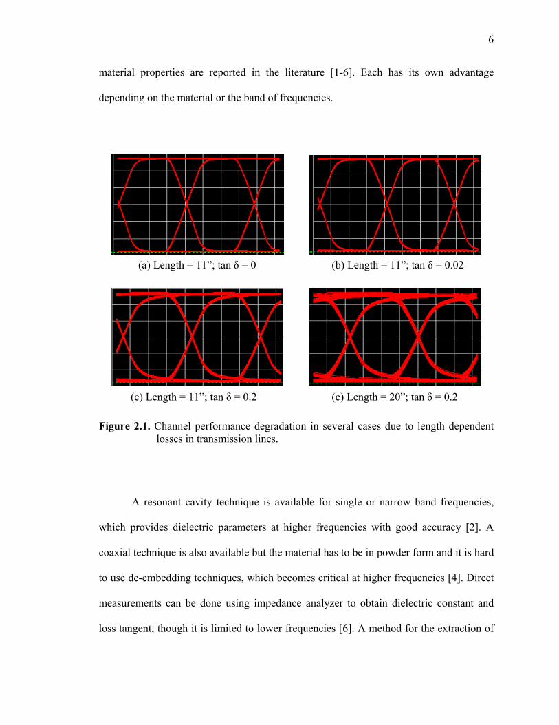
Section is shown in Figure 2.2.
8
Figure 2.2. General flow diagram for generating a new material parameter matrix.
The previously developed S-parameter extraction technique needed modification,
since for microstrip geometry, TEM wave propagation can no longer be assumed. This is
because of the presence of both air and the dielectric material as the propagation medium.
A quasi-TEM model [7] has to be used, which combines both dielectric mediums as a
single effective medium. Hence, only effective values of material properties could be
obtained from the normal extraction procedure. The algorithm was modified to obtain
practical values of material parameters. Two algorithms are presented in this Section for
extracting material parameters from a microstrip geometry. Both adopt the same
procedure as for stripline [1], but differ in the method of approximating conductor losses.
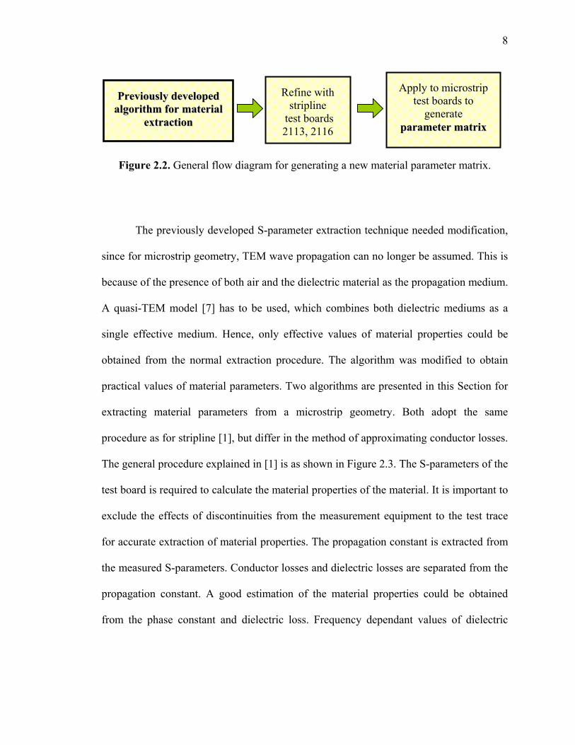
The general procedure explained in [1] is as shown in Figure 2.3. The S-parameters of the
test board is required to calculate the material properties of the material. It is important to
exclude the effects of discontinuities from the measurement equipment to the test trace
for accurate extraction of material properties. The propagation constant is extracted from
the measured S-parameters. Conductor losses and dielectric losses are separated from the
propagation constant. A good estimation of the material properties could be obtained
from the phase constant and dielectric loss. Frequency dependant values of dielectric
PPrreevviioouussllyy ddeevveellooppeedd aallggoorriitthhmm ffoorr mmaatteerriiaall
eexxttrraaccttiioonn
Refine with stripline
test boards 2113, 2116
Apply to microstrip test boards to
generate ppaarraammeetteerr mmaattrriixx
9
constant and loss tangent are obtained in this way. This work flow was used for the
extraction of material parameters from the designed microstrip test vehicles.
Figure 2.3. General procedure for extracting material parameters. 2.1. EXTRACTION OF MATERIAL PARAMETERS FROM STRIPLINE
Previously developed S-parameter algorithm for material extraction is revisited in
this section. Geometry is defined and traces were selected for measurements. S-parameter
and TDR measurements are taken. Data is analyzed and material properties are extracted.
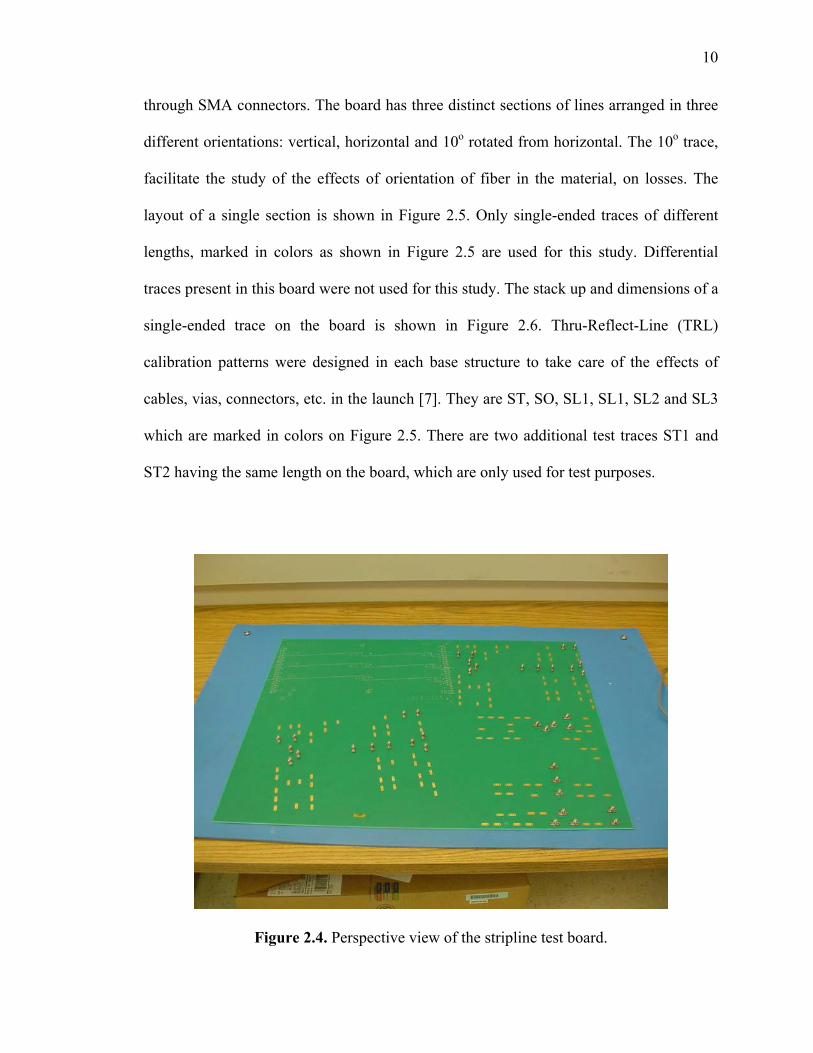
2.1.1. Description of Geometry. A perspective view of a 7-layer board under
test is shown in Figure 2.4. The board consists of stripline structures that are connected
Material Parameter Extraction
Measured S-parameters
Estimating conductor and dielectric losses of microstrip and stripline
εr and tan δ extraction
10
through SMA connectors. The board has three distinct sections of lines arranged in three
different orientations: vertical, horizontal and 10o rotated from horizontal. The 10o trace,
facilitate the study of the effects of orientation of fiber in the material, on losses. The
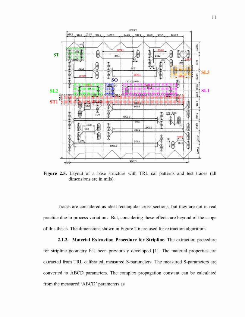
layout of a single section is shown in Figure 2.5. Only single-ended traces of different
lengths, marked in colors as shown in Figure 2.5 are used for this study. Differential
traces present in this board were not used for this study. The stack up and dimensions of a
single-ended trace on the board is shown in Figure 2.6. Thru-Reflect-Line (TRL)
calibration patterns were designed in each base structure to take care of the effects of
cables, vias, connectors, etc. in the launch [7]. They are ST, SO, SL1, SL1, SL2 and SL3
which are marked in colors on Figure 2.5. There are two additional test traces ST1 and
ST2 having the same length on the board, which are only used for test purposes.
Figure 2.4. Perspective view of the stripline test board.
11
Figure 2.5. Layout of a base structure with TRL cal patterns and test traces (all
dimensions are in mils).
Traces are considered as ideal rectangular cross sections, but they are not in real
practice due to process variations. But, considering these effects are beyond of the scope
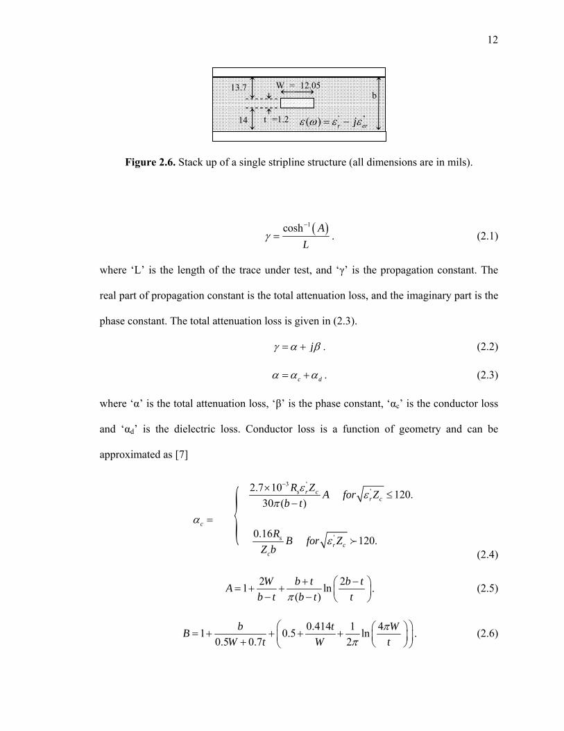
of this thesis. The dimensions shown in Figure 2.6 are used for extraction algorithms.
2.1.2. Material Extraction Procedure for Stripline. The extraction procedure
for stripline geometry has been previously developed [1]. The material properties are
extracted from TRL calibrated, measured S-parameters. The measured S-parameters are
converted to ABCD parameters. The complex propagation constant can be calculated
from the measured ‘ABCD’ parameters as
ST
SO
ST1
SL1 SL2
SL3
12
Figure 2.6. Stack up of a single stripline structure (all dimensions are in mils).
( )1cosh AL
γ−
= . (2.1)
where ‘L’ is the length of the trace under test, and ‘γ’ is the propagation constant. The
real part of propagation constant is the total attenuation loss, and the imaginary part is the
phase constant. The total attenuation loss is given in (2.3).
jγ α β= + . (2.2)
c dα α α= + . (2.3)
where ‘α’ is the total attenuation loss, ‘β’ is the phase constant, ‘αc’ is the conductor loss
and ‘αd’ is the dielectric loss. Conductor loss is a function of geometry and can be
approximated as [7]
(2.4)
2 21 ln( )
W b t b tAb t b t tπ
+ −⎛ ⎞= + + ⎜ ⎟− − ⎝ ⎠. (2.5)
0.414 1 41 0.5 ln0.5 0.7 2
b t WBW t W t
ππ
⎛ ⎞⎛ ⎞= + + + + ⎜ ⎟⎜ ⎟+ ⎝ ⎠⎝ ⎠. (2.6)
3 ''2.7 10 120.
30 ( )s r c
r cR Z A for Z
b tε ε
π
−×≤
−
'0.16 120.sr c
c
R B for ZZ b
ε
cα =
' ''( ) r erjε ω ε ε= −
13.7
14 t =1.2
W = 12.05b

13
where εr’ is the real part of permittivity, ‘Zc’ is the characteristic impedance of the line,
‘W’ is the width of the trace, ‘b’ is the thickness of the dielectric medium, ‘t’ is the
thickness of the trace, which could be observed in Figure 2.6. Surface resistance, ‘Rs’ is
given by
2sR ωμσ
= . (2.7)
where ‘μ’ is the permeability and ‘σ’ is the conductivity of the stripline conductor
material. Then, from the measured S-parameters total loss can be extracted. Conductor
loss can be approximated using (2.4). Therefore, dielectric loss can be calculated as
d cα α α= − . (2.8)
The real and imaginary part of permittivity is related to the phase constant and dielectric
loss as
( )2
' 2 22 d
cε β αω
= − . (2.9)
( )2
''2 2 d
cε α βω
= . (2.10)
' ''( ) jε ω ε ε= − . (2.11)
The loss tangent is defined as
''
'tan ( ) εδ ωε
= . (2.12)
The material extraction procedure explained above is shown in detail on Figure
2.7. The corresponding geometry is also shown in Figure 2.7, for the calculation of
conductor loss.
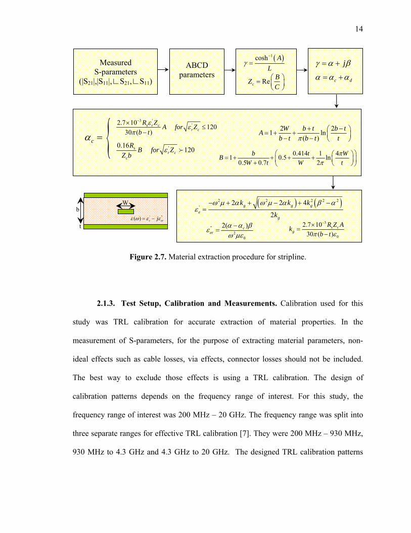
14
Figure 2.7. Material extraction procedure for stripline.
2.1.3. Test Setup, Calibration and Measurements. Calibration used for this
study was TRL calibration for accurate extraction of material properties. In the
measurement of S-parameters, for the purpose of extracting material parameters, non-
ideal effects such as cable losses, via effects, connector losses should not be included.
The best way to exclude those effects is using a TRL calibration. The design of
calibration patterns depends on the frequency range of interest. For this study, the
frequency range of interest was 200 MHz – 20 GHz. The frequency range was split into
three separate ranges for effective TRL calibration [7]. They were 200 MHz – 930 MHz,
930 MHz to 4.3 GHz and 4.3 GHz to 20 GHz. The designed TRL calibration patterns
( )1cosh AL
γ−
=ABCD parameters
RecBZC
⎛ ⎞= ⎜ ⎟⎝ ⎠
c dα α α= +
jγ α β= +
( ) ( )2 2 2 2 2'
2 2 4
2g g g
eg
k k k
k
ω μ α ω μ α β αε
− + + − + −=
''2
0
2( )cer
α α βεω με−
=
Measured S-parameters
(|S21|,|S11|,∟S21,∟S11)
' ''( ) r erjε ω ε ε= −
W
t
b
3
0
2.7 1030 ( )
s cg
R Z Akb tπ ε
−×=
−
3 ''2.7 10 120
30 ( )s r c
r cR Z A for Z
b tε ε
π
−×≤
−
'0.16 120sr c
c
R B for ZZ b
ε
2 21 ln( )
W b t b tAb t b t tπ
+ −⎛ ⎞= + + ⎜ ⎟− − ⎝ ⎠
0.414 1 41 0.5 ln0.5 0.7 2
b t WBW t W t
ππ
⎛ ⎞⎛ ⎞= + + + + ⎜ ⎟⎜ ⎟+ ⎝ ⎠⎝ ⎠
cα =
15
lengths are shown in Table 2.1. The purpose and procedure for designing TRL calibration
patterns for microstrip is explained later in Section 2.2.4.
Table 2.1. TRL calibration lengths and other trace lengths for patterns on the PCB.
ST (mils) SO (mils) SL1 (mils) SL2 (mils) SL3 (mils) ST1(mils) ST2(mils)
1000 500 3679.1 1578.9 1124.6 8976.4 8976.4
S-parameter measurements need to be taken for the test boards under
consideration. Two test boards with different dielectric material were studied. The
dielectric materials used in the board construction varied based on their resin content.
They were named Board 2113 and Board 2116. The stripline traces were extended
outside using SMA connectors for measuring S-parameters. The purpose of this
measurement is to extract dielectric constant and loss tangent as a function of frequency.
The boards have three different orientations of a base structure as shown in Figure 2.4.
The test setup involves an HP8270D network analyzer, high-precision microwave
cables, and test boards. Molex, press fit connectors were used to connect to the stripline.
Torque wrench was used as a part of measurement protocol to tighten the screws. This
helped to make sure that the same pressure is provided to the connectors each time the
connection was made. This is very important while considering TRL calibration. Figure
2.8 shows a typical measurement setup. High-precision microwave cables are used to
reduce the losses that accrue due to the cable itself. TRL calibration assumes that both
ports are identical so it is also important that the cables have identical characteristics.
16
Figure 2.8. Test setup used for stripline measurements.
TRL calibration was done on all three test pattern orientations. Calibration
included separate measurements on three different frequency ranges. All the data
obtained after measurements on the three frequency ranges were combined to span the
entire frequency range. S-parameters of Board 2113 and Board 2116 were measured and
the measured data were analyzed for errors as shown below. As a part of measurement
protocol, a sanity check for effective calibration was done. |S11| and |S21| were analyzed
for the “Thru” calibration standard. The expected and observed results are discussed
below. This protocol was used for all the measurements but only |S11| and |S21| data for
three orientations for Board 2113 are shown in Figure 2.9.
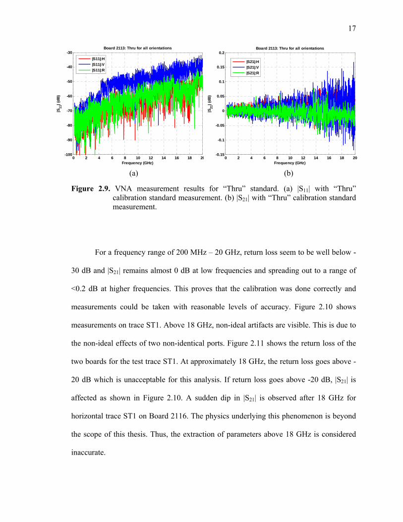
17
Figure 2.9. VNA measurement results for “Thru” standard. (a) |S11| with “Thru”
calibration standard measurement. (b) |S21| with “Thru” calibration standard measurement.
For a frequency range of 200 MHz – 20 GHz, return loss seem to be well below -
30 dB and |S21| remains almost 0 dB at low frequencies and spreading out to a range of
<0.2 dB at higher frequencies. This proves that the calibration was done correctly and
measurements could be taken with reasonable levels of accuracy. Figure 2.10 shows
measurements on trace ST1. Above 18 GHz, non-ideal artifacts are visible. This is due to
the non-ideal effects of two non-identical ports. Figure 2.11 shows the return loss of the
two boards for the test trace ST1. At approximately 18 GHz, the return loss goes above -
20 dB which is unacceptable for this analysis. If return loss goes above -20 dB, |S21| is
affected as shown in Figure 2.10. A sudden dip in |S21| is observed after 18 GHz for
horizontal trace ST1 on Board 2116. The physics underlying this phenomenon is beyond
the scope of this thesis. Thus, the extraction of parameters above 18 GHz is considered
inaccurate.
(a) (b)
0 2 4 6 8 10 12 14 16 18 20-100
-90
-80
-70
-60
-50
-40
-30Board 2113: Thru for all orientations
Frequency (GHz)
|S11
| (dB
)
|S11|:H|S11|:V|S11|:R
0 2 4 6 8 10 12 14 16 18 20-0.15
-0.1
-0.05
0
0.05
0.1
0.15
0.2Board 2113: Thru for all orientations
Frequency (GHz)
|S21
| (dB
)
|S21|:H|S21|:V|S21|:R
18
Figure 2.10. Measured |S21| of the test trace ST1.
Figure 2.11. Measured |S11| of the trace ST1.
0 2 4 6 8 10 12 14 16 18 20
-16
-14
-12
-10
-8
-6
-4
-2
0
Frequency (GHz)
|S21
| (dB
)
H-2113V-2113R-2113H-2116V-2116R-2116
0 2 4 6 8 10 12 14 16 18 20-70
-60
-50
-40
-30
-20
-10
Frequency (GHz)
|S11
| (dB
)
H-2113V-2113R-2113H-2116V-2116R-2116
19
As mentioned earlier, the test board consisted of three different orientations:
vertical, horizontal and 10o rotated from horizontal. Each section had its own calibration
patterns because for TRL calibration results may vary even with the different weave
effects of the fiber in the material. Measurements were done on all three orientations to
study the effects due to orientation of the traces in the board. Figure 2.10 shows some
difference in the |S21| due to orientation of traces. But, the analysis of the underlying
physics is beyond the scope of this thesis.
Ideally, the measurements taken after switching port locations should be the
identical. This was true in measurements, because |S12| and |S21| were always almost
equal. But, in real world, none of the ports will be exactly the same. So, measurements
were taken after switching the ports to see if there are any variations. Figure 2.12 shows
that |S12| and |S21| are same even after switching ports.
In the extraction procedure, it is assumed that the impedance of the trace stays
constant, along the length of the trace. Ideally it should be constant. Because of the
change in width and dielectric thickness due to process variations, the impedance varies
at different locations along the trace. So, it becomes important to observe if the
impedance variation is small and is close to 50Ω. Cross-sections of these geometries
could provide us a better understanding of the variation. But it is a painful and hard
process. Time domain reflectometry (TDR) measurements are a good way to analyze the
impedance variation along the length of a trace. Every single trace on the board was
analyzed using TDR measurements and the impedance variation stayed within 48-53Ω.
Though, for extraction procedure, the mean value of the impedance is taken into
consideration for calculations. The test setup and procedure is explained below.
20
0 2 4 6 8 10 12 14 16 18 20-16
-14
-12
-10
-8
-6
-4
-2
0Test Trace 1
Frequency (GHz)
|S21
| & |S
12| (
dB)
|S21|:H-2113
|S12|:H-2113
|S21|:H-2116
|S12|:H-2116
Figure 2.12. |S21| and |S12| comparison after ports were switched manually.
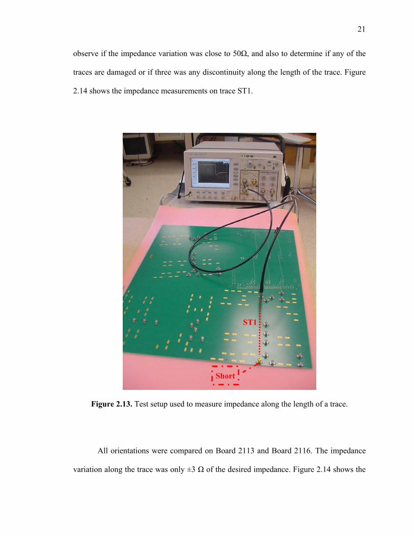
The test setup used to measure impedance along the trace is shown in Figure 2.13.
One port of TDR was connected to the trace and the other end of the trace was shorted
using a “Short” calibration standard. TDR sends out a pulse through the transmission line
which was reflected from the other end of the trace with a reflection coefficient of -1
(short). The impedance was calculated based on the reflection coefficient at various
locations on the trace. These measurements were taken on all the traces including the
calibration traces, on all three orientations of boards 2113 and 2116. This was done to
10.5 10.55 10.6 10.65 10.7 10.75 10.8 10.85 10.9 10.95 11
-8.15
-8.1
-8.05
-8
-7.95
-7.9
-7.85
-7.8
-7.75
-7.7
-7.65
Test Trace 1
Frequency (GHz)
|S21
| & |S
12| (
dB)
|S21|:H-2113
|S12|:H-2113
|S21|:H-2116
|S12|:H-2116
9.15 9.2 9.25 9.3 9.35 9.4 9.45 9.5 9.55
-8
-7.95
-7.9
-7.85
-7.8
-7.75
-7.7
-7.65Test Trace 1
Frequency (GHz)
|S21
| & |S
12| (
dB)
|S21|:H-2113
|S12|:H-2113
|S21|:H-2116
|S12|:H-2116
21
observe if the impedance variation was close to 50Ω, and also to determine if any of the
traces are damaged or if three was any discontinuity along the length of the trace. Figure
2.14 shows the impedance measurements on trace ST1.
Figure 2.13. Test setup used to measure impedance along the length of a trace.
All orientations were compared on Board 2113 and Board 2116. The impedance
variation along the trace was only ±3 Ω of the desired impedance. Figure 2.14 shows the
Short
ST1
22
actual measurements. Enlarged views of capacitive connector discontinuity and
impedance variation along the trace are also shown in Figure 2.14.
59.3 59.305 59.31 59.315 59.32 59.325 59.33 59.335 59.34 59.345 59.350
10
20
30
40
50
60Test 1
Time(ns)
Impe
danc
e ( Ω
)
cableH-2113V-2113R-2113H-2116V-2116R-2116
Figure 2.14. TDR measurements on trace ST1. (a) TDR Impedance measurement along the trace length of ST1. (b) Capacitive connector discontinuity (c) Enlarged view of impedance variation along the trace.
2.1.4. Extracted Results and Analysis. The measured data was analyzed with a
TDR for its discontinuity. The |S21| and |S11| of the “Thru” calibration standard was within
(b) (c)
59.304 59.3045 59.305 59.3055 59.306 59.3065 59.307 59.3075
44
45
46
47
48
49
50
51
52Test 1
Time(ns)
cableH-2113V-2113R-2113H-2116V-2116R-2116
59.31 59.315 59.32 59.325 59.33 59.335
49
50
51
52
53
54
55
56Test 1
Time(ns)
cableH-2113V-2113R-2113H-2116V-2116R-2116
(a)
23
acceptable limits as discussed in Section 2.1.3. The |S21| and |S11| of the measured test
traces were also in acceptable limits as discussed in Section 2.1.3. Then, measurement
data was used for extracting the material properties using the algorithm detailed in
Section 2.1.2. Measured S-parameters were used to calculate dielectric constant and loss
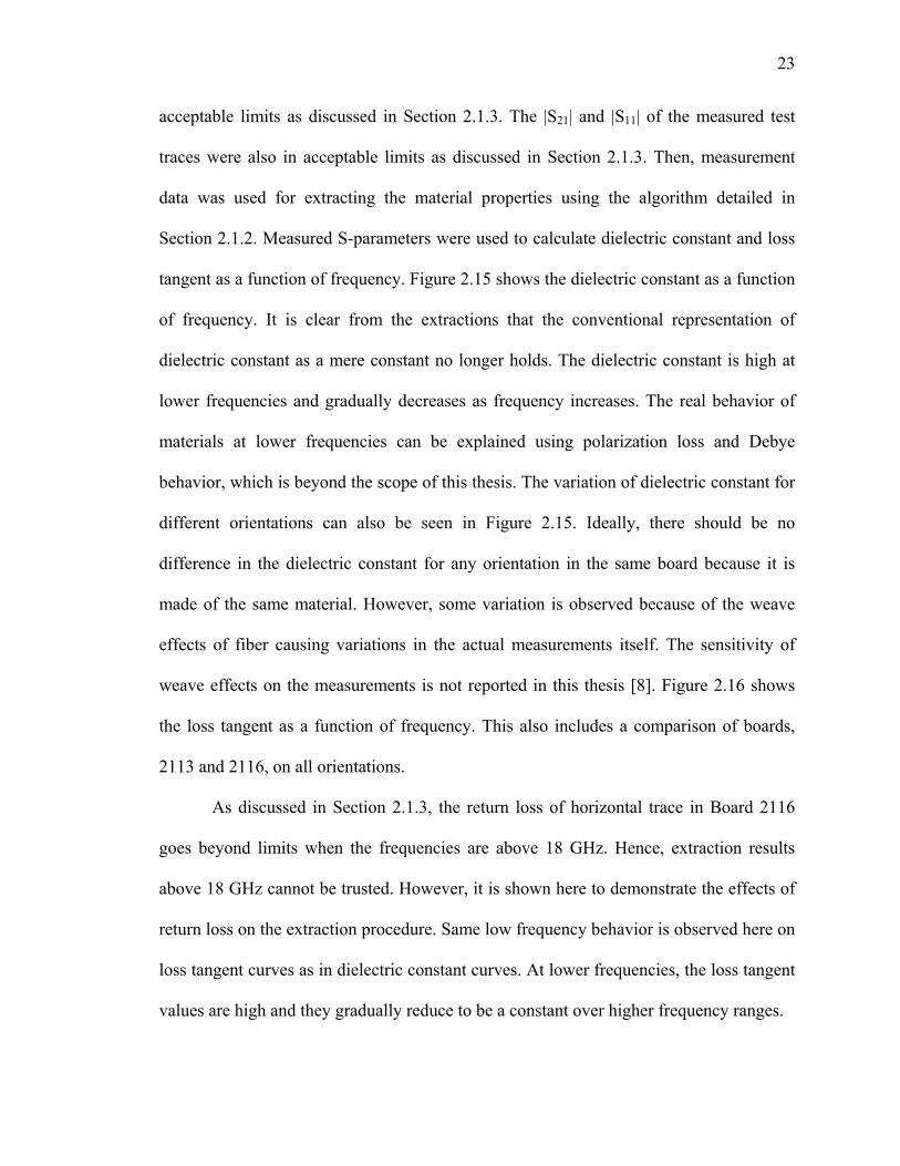
tangent as a function of frequency. Figure 2.15 shows the dielectric constant as a function
of frequency. It is clear from the extractions that the conventional representation of
dielectric constant as a mere constant no longer holds. The dielectric constant is high at
lower frequencies and gradually decreases as frequency increases. The real behavior of
materials at lower frequencies can be explained using polarization loss and Debye
behavior, which is beyond the scope of this thesis. The variation of dielectric constant for
different orientations can also be seen in Figure 2.15. Ideally, there should be no
difference in the dielectric constant for any orientation in the same board because it is
made of the same material. However, some variation is observed because of the weave
effects of fiber causing variations in the actual measurements itself. The sensitivity of
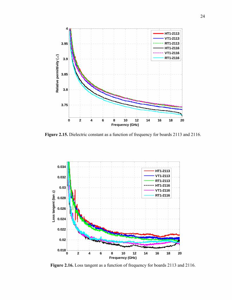
weave effects on the measurements is not reported in this thesis [8]. Figure 2.16 shows
the loss tangent as a function of frequency. This also includes a comparison of boards,
2113 and 2116, on all orientations.
As discussed in Section 2.1.3, the return loss of horizontal trace in Board 2116
goes beyond limits when the frequencies are above 18 GHz. Hence, extraction results
above 18 GHz cannot be trusted. However, it is shown here to demonstrate the effects of
return loss on the extraction procedure. Same low frequency behavior is observed here on
loss tangent curves as in dielectric constant curves. At lower frequencies, the loss tangent
values are high and they gradually reduce to be a constant over higher frequency ranges.
24
Figure 2.15. Dielectric constant as a function of frequency for boards 2113 and 2116.
Figure 2.16. Loss tangent as a function of frequency for boards 2113 and 2116.
0 2 4 6 8 10 12 14 16 18 20
3.75
3.8
3.85
3.9
3.95
4
Frequency (GHz)
Rel
ativ
e pe
rmitt
ivity
(ε, )
HT1-2113VT1-2113RT1-2113HT1-2116VT1-2116RT1-2116
0 2 4 6 8 10 12 14 16 18 200.018
0.02
0.022
0.024
0.026
0.028
0.03
0.032
0.034
Frequency (GHz)
Loss
tang
ent (
tan δ)
HT1-2113VT1-2113RT1-2113HT1-2116VT1-2116RT1-2116
25
2.2. EXTRACTION OF MATERIAL PARAMETERS FROM MICROSTRIP
As discussed in Section 2.1, the material properties of stripline geometry can be
extracted directly from S-parameter measurements. This is fairly a straight forward
process for stripline structure, since the field is contained and there is only one dielectric
medium. Therefore, TEM mode of wave propagation can be assumed. But, when
microstrip geometry is considered, mode of propagation of the waves is not TEM
anymore. The dielectric material and air act as medium of propagation. For most of the
operating frequency range of microstrips, the longitudinal components of the fields for
the dominant mode are very much smaller than the transverse components. So, the
transverse components can be neglected. The dominant mode then behaves like TEM
mode and this approximation is called the Quasi-TEM approximation [7]. An effective
permittivity and effective loss tangent as function of frequency were considered in this
case. Literature also provides closed form expressions to calculate the practical values of
material properties which will be discussed later.
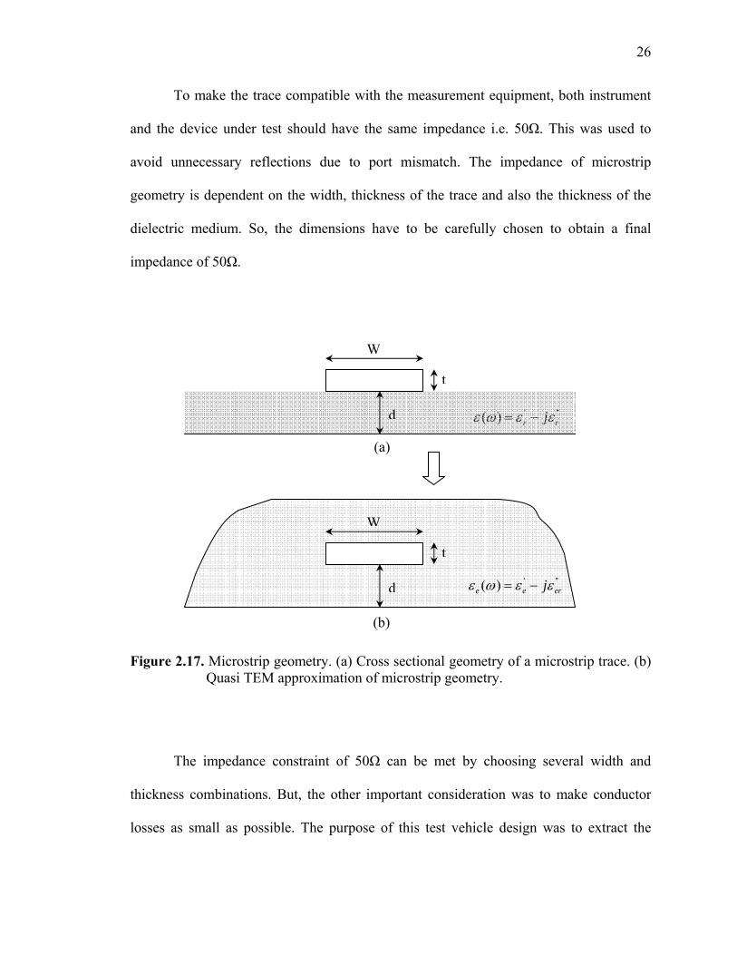
2.2.1. Geometry and Test Vehicle Design. As discussed earlier, for microstrip
geometry, Quasi TEM approach is used and the new geometry would be represented as
shown in Figure 2.17.
In order to validate the new microstrip extraction procedure, specific microstrip
test vehicles were designed. To design a test vehicle for material parameter extraction,
several characteristics needs to be analyzed. Only the material is of interest and other
non-ideal artifacts should be avoided to the greatest extent. Some of the important
characteristics are analyzed in detail below. This analysis helps in building up geometry
with approximate dimensions.
26
To make the trace compatible with the measurement equipment, both instrument
and the device under test should have the same impedance i.e. 50Ω. This was used to
avoid unnecessary reflections due to port mismatch. The impedance of microstrip
geometry is dependent on the width, thickness of the trace and also the thickness of the
dielectric medium. So, the dimensions have to be carefully chosen to obtain a final
impedance of 50Ω.
Figure 2.17. Microstrip geometry. (a) Cross sectional geometry of a microstrip trace. (b)
Quasi TEM approximation of microstrip geometry.
The impedance constraint of 50Ω can be met by choosing several width and
thickness combinations. But, the other important consideration was to make conductor
losses as small as possible. The purpose of this test vehicle design was to extract the
' ''( ) r rjε ω ε ε= −
' ''( )e e erjε ω ε ε= −
W
t
d
W
t
d
(a)
(b)
27
material properties of the dielectric material between the conductors. So, it became
important to make the dielectric loss dominate over the frequency range of interest. This
was achieved by doing the cross-over point analysis. The cross-over point is the
frequency at which there is equal contribution of conductor loss and dielectric loss. The
ratio of dielectric loss to conductor loss is 1 at the cross over point.
1d
c
αα
= . (2.13)
where ‘αd’ is the dielectric loss and ‘αc’ is the conductor loss.
So, the idea was to choose the dimensions in such a way that the cross over point
appears at very low frequencies. This analysis can be done using two methods. One was
to use analytical expressions of loss parameters to calculate the cross over point [9]. The
other method was to use static solvers such as Hyperlynx which calculates the loss curves
directly.
Taking the impedance and cross over point into consideration the following
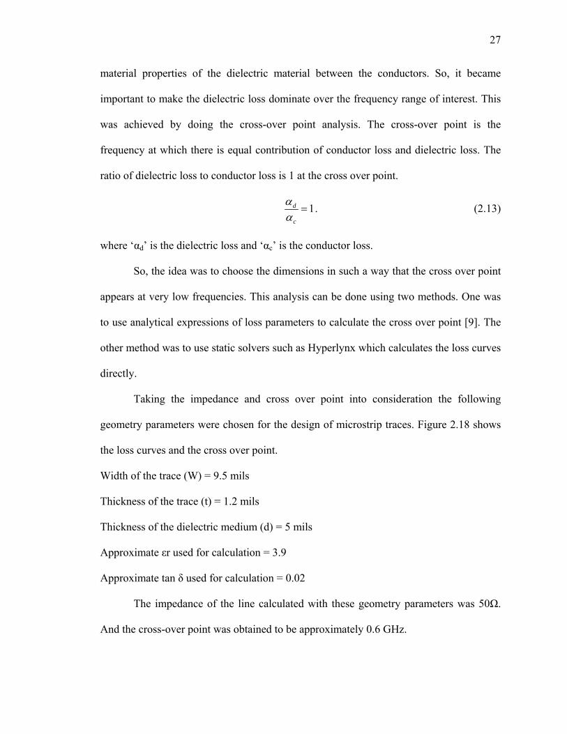
geometry parameters were chosen for the design of microstrip traces. Figure 2.18 shows
the loss curves and the cross over point.
Width of the trace (W) = 9.5 mils
Thickness of the trace (t) = 1.2 mils
Thickness of the dielectric medium (d) = 5 mils
Approximate εr used for calculation = 3.9
Approximate tan δ used for calculation = 0.02
The impedance of the line calculated with these geometry parameters was 50Ω.
And the cross-over point was obtained to be approximately 0.6 GHz.
28
Figure 2.18. Loss curves obtained after using the current geometry parameters with the
cross over point at 0.6 GHz.
The frequency range of interest for this project was 0-20 GHz. However, it was
important to make sure that the design was compatible for such high frequency range.
The following are three frequency considerations that were taken into account. These
considerations were also used in the design of stripline test vehicles [11] discussed in
Section 2.1.1.
Three mechanisms may limit the application frequencies of microstrip lines:
higher-order modes, surface wave propagation in the planar metal-dielectric-air structure,
and radiation effects in the open structure [10]. It is reasonable to estimate the upper
frequency limit based on the three mechanisms, and take the lowest value as the upper-
bound of the interest frequency. The cutoff frequency for the first higher-order mode was
estimated as
( )
0' 2 0.8
c
e
cfW dε
=+
. (2.14)
Cross over point at 0.6GHz
1d
c
αα
=
dα ω∼
cα ω∼
29
where ‘co’ is the speed of light in free space. The lowest TM surface mode has no cutoff
frequency, but its coupling to the quasi-TEM mode becomes significant only when their
phase velocities are nearly matched. This occurs at the frequency
( )'
0
'
arctan
2 1e
s
e
cf
d
ε
π ε=
−. (2.15)
An approximate relation for the frequency where the radiation becomes significant was
'42.14 e
rf dε
> . (2.16)
where rf is in GHz, and d is in millimeters.
For the test board considered, Table 2.2 provides the values of frequencies
mentioned on (2.14), (2.15), and (2.16). It is clear from Table 2.2 that the required
frequency range of 0-20 GHz opposes no limitations.
Table 2.2. Frequency limitations for the microstrip test vehicle design.
cf 260 GHz
sf 412 GHz
rf 24 GHz
The purpose of this test vehicle was to provide information of the dielectric
material used for its construction. Hence, the measurements should only depict effects of
the dielectric. It was not desirable to have non-ideal effects of cables, vias and connectors
on measurements. Thus, TRL calibration technique was used to de-embed the effects of
30
such non-idealities. With the conventional measurement setup, the reference plane can
only be set within the measurement equipment. The actual measurement will include
effect of vias, probes, connectors etc. which will degrade the measurement results. But,
with TRL calibration technique [7], the reference plane can be set at a desired point on
the device under test. This calibration procedure characterizes the error boxes associated
with the discontinuities till the device under test, setting the reference plane at a desired
point. The TRL calibration patterns were designed the following way.
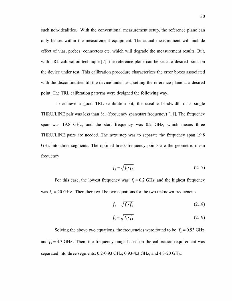
To achieve a good TRL calibration kit, the useable bandwidth of a single
THRU/LINE pair was less than 8:1 (frequency span/start frequency) [11]. The frequency
span was 19.8 GHz, and the start frequency was 0.2 GHz, which means three
THRU/LINE pairs are needed. The next step was to separate the frequency span 19.8
GHz into three segments. The optimal break-frequency points are the geometric mean
frequency
1 2jf f f= i (2.17)
For this case, the lowest frequency was 1 0.2 GHzf = and the highest frequency
was 4 20 GHzf = . Then there will be two equations for the two unknown frequencies
2 1 3f f f= i (2.18)
3 2 4f f f= i (2.19)
Solving the above two equations, the frequencies were found to be 2 0.93 GHzf =
and 3 4.3 GHzf = . Then, the frequency range based on the calibration requirement was
separated into three segments, 0.2-0.93 GHz, 0.93-4.3 GHz, and 4.3-20 GHz.
31
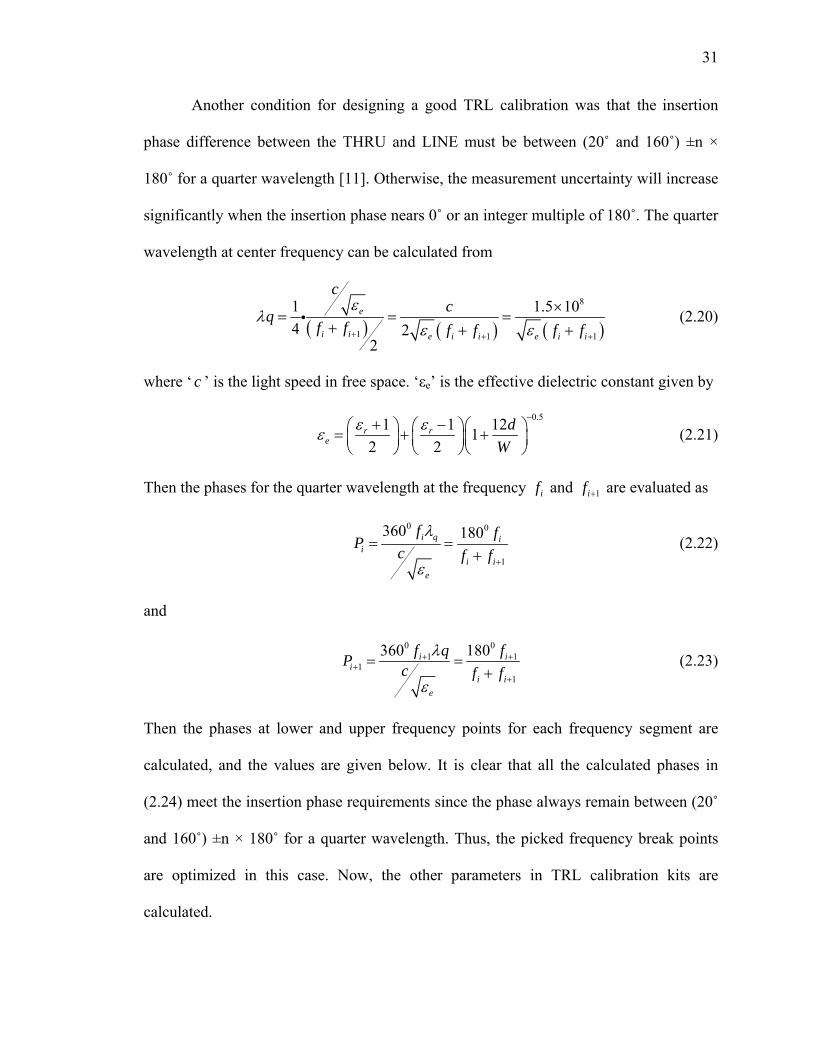
Another condition for designing a good TRL calibration was that the insertion
phase difference between the THRU and LINE must be between (20˚ and 160˚) ±n ×
180˚ for a quarter wavelength [11]. Otherwise, the measurement uncertainty will increase
significantly when the insertion phase nears 0˚ or an integer multiple of 180˚. The quarter
wavelength at center frequency can be calculated from
( ) ( ) ( )
8
1 1 1
1 1.5 104 2
2
e
i i e i i e i i
ccq
f f f f f fε
λε ε+ + +
×= = =
+ + +i (2.20)
where ‘ c ’ is the light speed in free space. ‘εe’ is the effective dielectric constant given by
0.51 1 121
2 2r r
ed
Wε εε
−+ −⎛ ⎞ ⎛ ⎞⎛ ⎞= + +⎜ ⎟⎜ ⎟ ⎜ ⎟⎝ ⎠⎝ ⎠ ⎝ ⎠
(2.21)
Then the phases for the quarter wavelength at the frequency if and 1if + are evaluated as
0 0
1
360 180i q ii
i ie
f fP c f fλ
ε +
= =+
(2.22)
and
0 0
1 11
1
360 180i ii
i ie
f q fP c f fλ
ε
+ ++
+
= =+
(2.23)
Then the phases at lower and upper frequency points for each frequency segment are
calculated, and the values are given below. It is clear that all the calculated phases in
(2.24) meet the insertion phase requirements since the phase always remain between (20˚
and 160˚) ±n × 180˚ for a quarter wavelength. Thus, the picked frequency break points
are optimized in this case. Now, the other parameters in TRL calibration kits are
calculated.
32
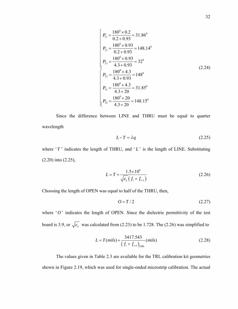
00
11
00
12
00
21
00
22
00
31
00
32
180 0.2 31.860.2 0.93180 0.93 148.140.2 0.93
180 0.93 324.3 0.93
180 4.3 1484.3 0.93180 4.3 31.854.3 20
180 20 148.154.3 20
P
P
P
P
P
P
⎧ ×= =⎪ +⎪
×⎪= =⎪ +⎪
×⎪ = =⎪⎪ +⎨
×⎪ = =⎪ +⎪
×⎪ = =⎪ +⎪ ×⎪ = =⎪ +⎩
(2.24)
Since the difference between LINE and THRU must be equal to quarter
wavelength
L T qλ− = (2.25)
where ‘T ’ indicates the length of THRU, and ‘ L ’ is the length of LINE. Substituting
(2.20) into (2.25),
( )
8
1
1.5 10
e i i
L Tf fε +
×= +
+ (2.26)
Choosing the length of OPEN was equal to half of the THRU, then,
/ 2O T= (2.27)
where ‘O ’ indicates the length of OPEN. Since the dielectric permittivity of the test
board is 3.9, or eε was calculated from (2.23) to be 1.728. The (2.26) was simplified to
( )1
3417.543( ) ( )i i GHz
L T mils milsf f +
= ++
(2.28)
The values given in Table 2.3 are available for the TRL calibration kit geometries
shown in Figure 2.19, which was used for single-ended microstrip calibration. The actual
33
board manufactured is shown in Figure 2.20. The landing pattern for each trace is also
shown in Figure 2.21.
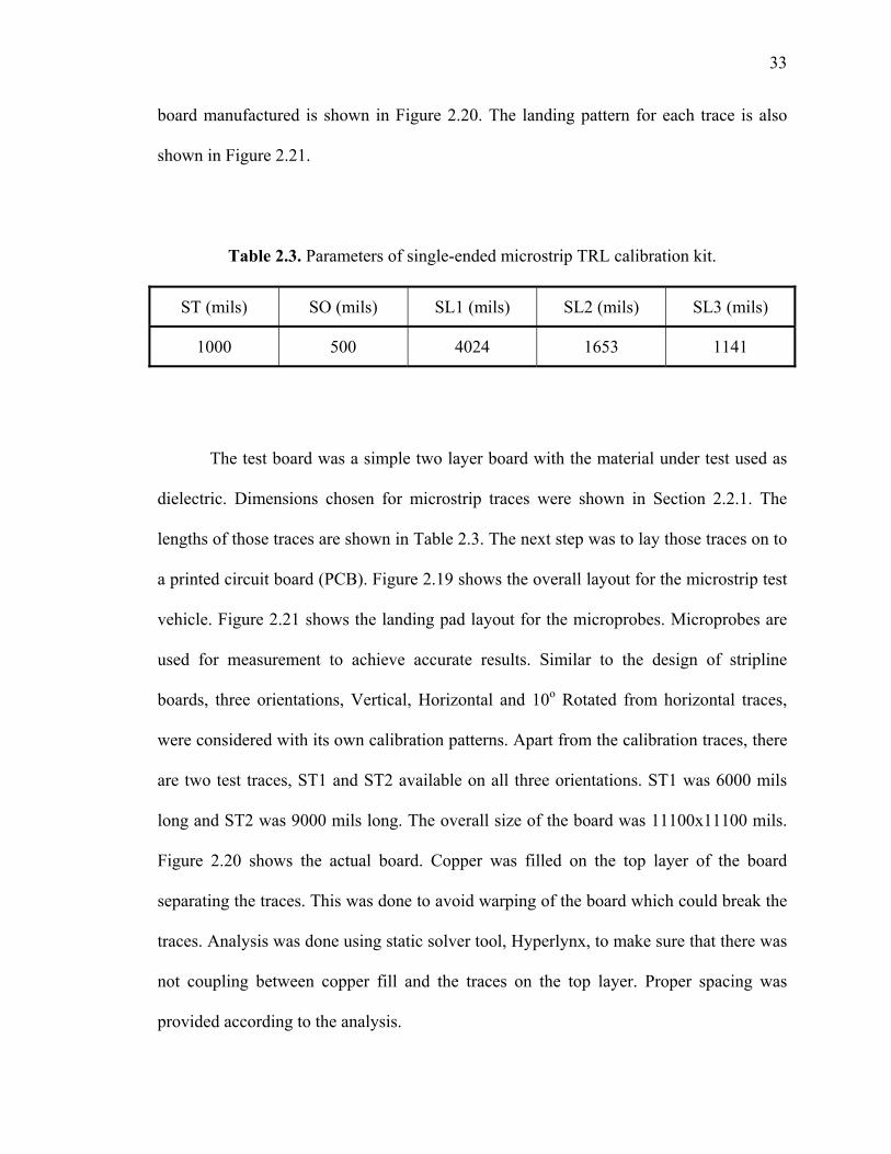
Table 2.3. Parameters of single-ended microstrip TRL calibration kit.
ST (mils) SO (mils) SL1 (mils) SL2 (mils) SL3 (mils)
1000 500 4024 1653 1141
The test board was a simple two layer board with the material under test used as
dielectric. Dimensions chosen for microstrip traces were shown in Section 2.2.1. The
lengths of those traces are shown in Table 2.3. The next step was to lay those traces on to
a printed circuit board (PCB). Figure 2.19 shows the overall layout for the microstrip test
vehicle. Figure 2.21 shows the landing pad layout for the microprobes. Microprobes are
used for measurement to achieve accurate results. Similar to the design of stripline
boards, three orientations, Vertical, Horizontal and 10o Rotated from horizontal traces,
were considered with its own calibration patterns. Apart from the calibration traces, there
are two test traces, ST1 and ST2 available on all three orientations. ST1 was 6000 mils
long and ST2 was 9000 mils long. The overall size of the board was 11100x11100 mils.
Figure 2.20 shows the actual board. Copper was filled on the top layer of the board
separating the traces. This was done to avoid warping of the board which could break the
traces. Analysis was done using static solver tool, Hyperlynx, to make sure that there was
not coupling between copper fill and the traces on the top layer. Proper spacing was
provided according to the analysis.
34
Figure 2.19. Microstrip test vehicle design including TRL calibration and test traces.
Figure 2.20. Actual board: microstrip test vehicle design.
35
Figure 2.21. Landing pad design for each trace.
A small section of the trace is shown at the bottom of Figure 2.21. The width of
the trace was increased at the edges to accommodate the probe tips. The pad includes a
via hole connected to the bottom copper layer. Enough room was also given there for
landing the probe tips. The probe pitch was chosen to be 1000μm. This probe turned out
to be very fragile and hard to use. But, there were also long traces in the design which
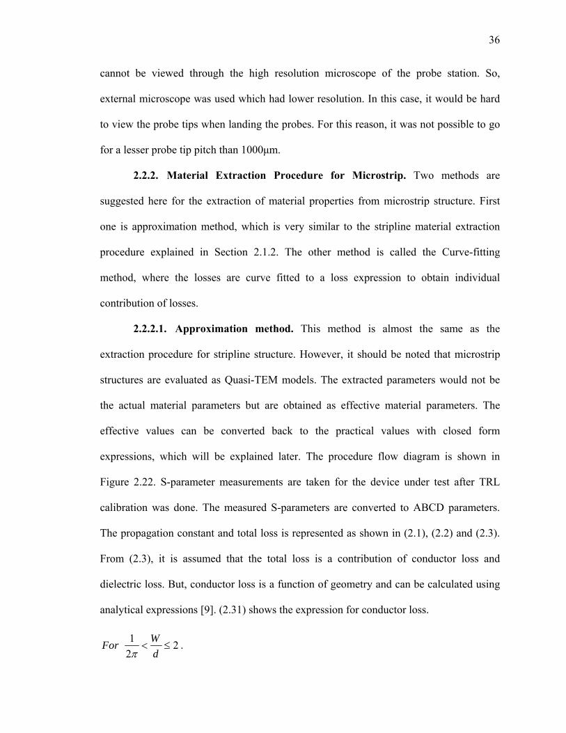
36
cannot be viewed through the high resolution microscope of the probe station. So,
external microscope was used which had lower resolution. In this case, it would be hard
to view the probe tips when landing the probes. For this reason, it was not possible to go
for a lesser probe tip pitch than 1000μm.
2.2.2. Material Extraction Procedure for Microstrip. Two methods are
suggested here for the extraction of material properties from microstrip structure. First
one is approximation method, which is very similar to the stripline material extraction
procedure explained in Section 2.1.2. The other method is called the Curve-fitting
method, where the losses are curve fitted to a loss expression to obtain individual
contribution of losses.
2.2.2.1. Approximation method. This method is almost the same as the
extraction procedure for stripline structure. However, it should be noted that microstrip
structures are evaluated as Quasi-TEM models. The extracted parameters would not be
the actual material parameters but are obtained as effective material parameters. The
effective values can be converted back to the practical values with closed form
expressions, which will be explained later. The procedure flow diagram is shown in
Figure 2.22. S-parameter measurements are taken for the device under test after TRL
calibration was done. The measured S-parameters are converted to ABCD parameters.
The propagation constant and total loss is represented as shown in (2.1), (2.2) and (2.3).
From (2.3), it is assumed that the total loss is a contribution of conductor loss and
dielectric loss. But, conductor loss is a function of geometry and can be calculated using
analytical expressions [9]. (2.31) shows the expression for conductor loss.
1 22
WFordπ
< ≤ .
37
where ‘W’ is the width of the trace, ‘d’ is the dielectric thickness and effective width is
'W W W= + Δ . (2.29)
where ‘ΔW’ is the correction term added to take into account of the thickness of the trace
[9] given by
2ln 1t dWtπ
⎛ ⎞Δ = +⎜ ⎟⎝ ⎠
. (2.30)
Figure 2.22. Material extraction algorithm (approximation technique) for microstrip.
1 22
WFordπ
< ≤
( ) 2'
' '
1ln 10 8.68 21 1 ln 1 /20 2 4 1
2
sc
c
tR W d d d d Np m
tZ d d W W td
απ π
⎧ ⎫⎡ ⎤⎛ ⎞+⎜ ⎟⎪ ⎪⎢ ⎥⎡ ⎤⎛ ⎞ ⎛ ⎞ ⎪ ⎪⎛ ⎞ ⎝ ⎠⎢ ⎥= − + + + −⎢ ⎥ ⎨ ⎬⎜ ⎟ ⎜ ⎟ ⎜ ⎟ ⎛ ⎞⎝ ⎠⎢ ⎥⎢ ⎥⎝ ⎠⎝ ⎠ ⎪ ⎪⎣ ⎦ +⎜ ⎟⎢ ⎥⎪ ⎪⎝ ⎠⎣ ⎦⎩ ⎭
2ln 1t dWtπ
⎛ ⎞Δ = +⎜ ⎟⎝ ⎠
'W W W= + Δ2sR ωμσ
=
( )1cosh AL
γ−
=ABCD parameters
RecBZC
⎛ ⎞= ⎜ ⎟⎝ ⎠
c dα α α= +
jγ α β= +Measured S-parameters
(|S21|,|S11|,∟S21,∟S11)
( )2
''2 2er d
cε α βω
=
( )2
' 2 22e d
cε β αω
= −
d cα α α= −
( )' ''0( ) e erjε ω ε ε ε= −
( )''
'tan ereff
e
εδε
=
1WFord≥ 121 dA
W= +
'' er
DC
εε⎛ ⎞−
= ⎜ ⎟⎝ ⎠
1 1 0.2172 2
tCA Wd
⎛ ⎞⎛ ⎞ ⎛ ⎞= + −⎜ ⎟ ⎜ ⎟ ⎜ ⎟⎝ ⎠ ⎝ ⎠ ⎝ ⎠
1 1 0.2172 2
tDA Wd
⎛ ⎞⎛ ⎞ ⎛ ⎞= − +⎜ ⎟ ⎜ ⎟ ⎜ ⎟⎝ ⎠ ⎝ ⎠ ⎝ ⎠
( ) '
1 1tan tan 11eff
r
AA
δ δε
⎡ ⎤−⎛ ⎞= +⎢ ⎥⎜ ⎟+⎝ ⎠⎣ ⎦
38
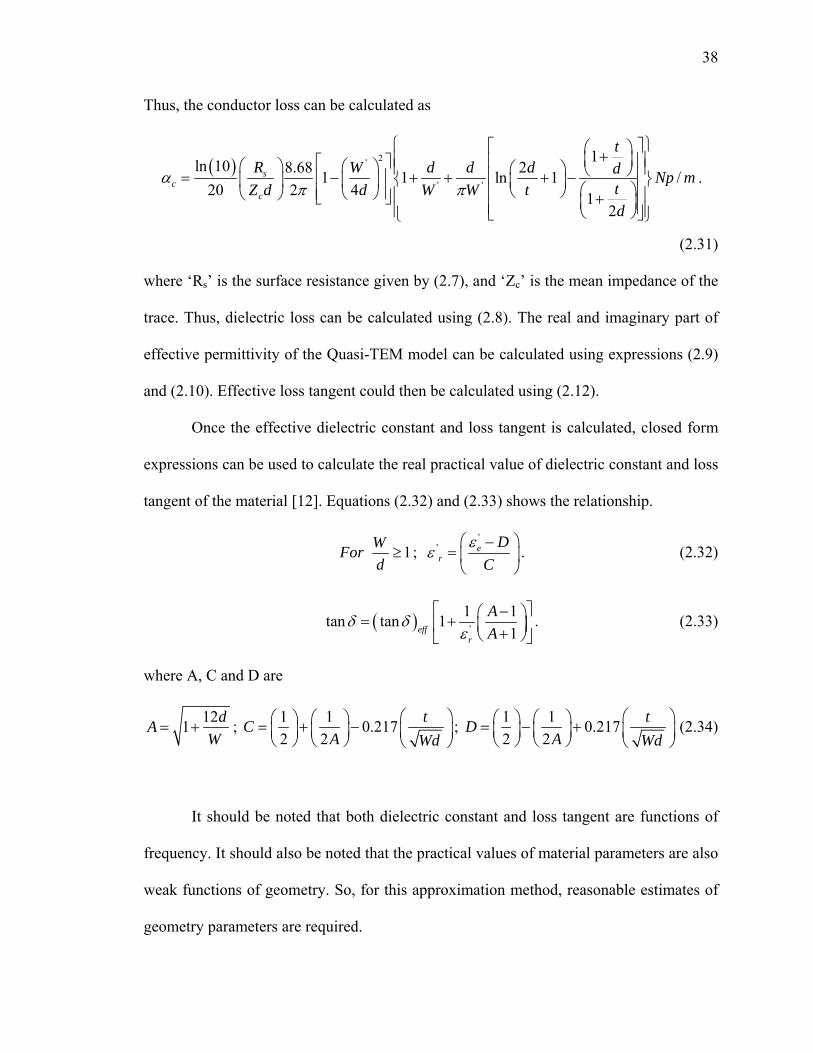
Thus, the conductor loss can be calculated as
( ) 2'
' '
1ln 10 8.68 21 1 ln 1 /20 2 4 1
2
sc
c
tR W d d d d Np m
tZ d d W W td
απ π
⎧ ⎫⎡ ⎤⎛ ⎞+⎜ ⎟⎪ ⎪⎢ ⎥⎡ ⎤⎛ ⎞ ⎛ ⎞ ⎪ ⎪⎛ ⎞ ⎝ ⎠⎢ ⎥= − + + + −⎢ ⎥ ⎨ ⎬⎜ ⎟ ⎜ ⎟ ⎜ ⎟ ⎛ ⎞⎝ ⎠⎢ ⎥⎢ ⎥⎝ ⎠⎝ ⎠ ⎪ ⎪⎣ ⎦ +⎜ ⎟⎢ ⎥⎪ ⎪⎝ ⎠⎣ ⎦⎩ ⎭
.
(2.31)
where ‘Rs’ is the surface resistance given by (2.7), and ‘Zc’ is the mean impedance of the
trace. Thus, dielectric loss can be calculated using (2.8). The real and imaginary part of
effective permittivity of the Quasi-TEM model can be calculated using expressions (2.9)
and (2.10). Effective loss tangent could then be calculated using (2.12).
Once the effective dielectric constant and loss tangent is calculated, closed form
expressions can be used to calculate the real practical value of dielectric constant and loss
tangent of the material [12]. Equations (2.32) and (2.33) shows the relationship.
1WFord≥ ;
'' er
DC
εε⎛ ⎞−
= ⎜ ⎟⎝ ⎠
. (2.32)
( ) '
1 1tan tan 11eff
r
AA
δ δε
⎡ ⎤−⎛ ⎞= +⎢ ⎥⎜ ⎟+⎝ ⎠⎣ ⎦. (2.33)
where A, C and D are
121 dAW
= + ; 1 1 0.2172 2
tCA Wd
⎛ ⎞⎛ ⎞ ⎛ ⎞= + −⎜ ⎟ ⎜ ⎟ ⎜ ⎟⎝ ⎠ ⎝ ⎠ ⎝ ⎠; 1 1 0.217
2 2tD
A Wd⎛ ⎞⎛ ⎞ ⎛ ⎞= − +⎜ ⎟ ⎜ ⎟ ⎜ ⎟⎝ ⎠ ⎝ ⎠ ⎝ ⎠
(2.34)
It should be noted that both dielectric constant and loss tangent are functions of
frequency. It should also be noted that the practical values of material parameters are also
weak functions of geometry. So, for this approximation method, reasonable estimates of
geometry parameters are required.
39
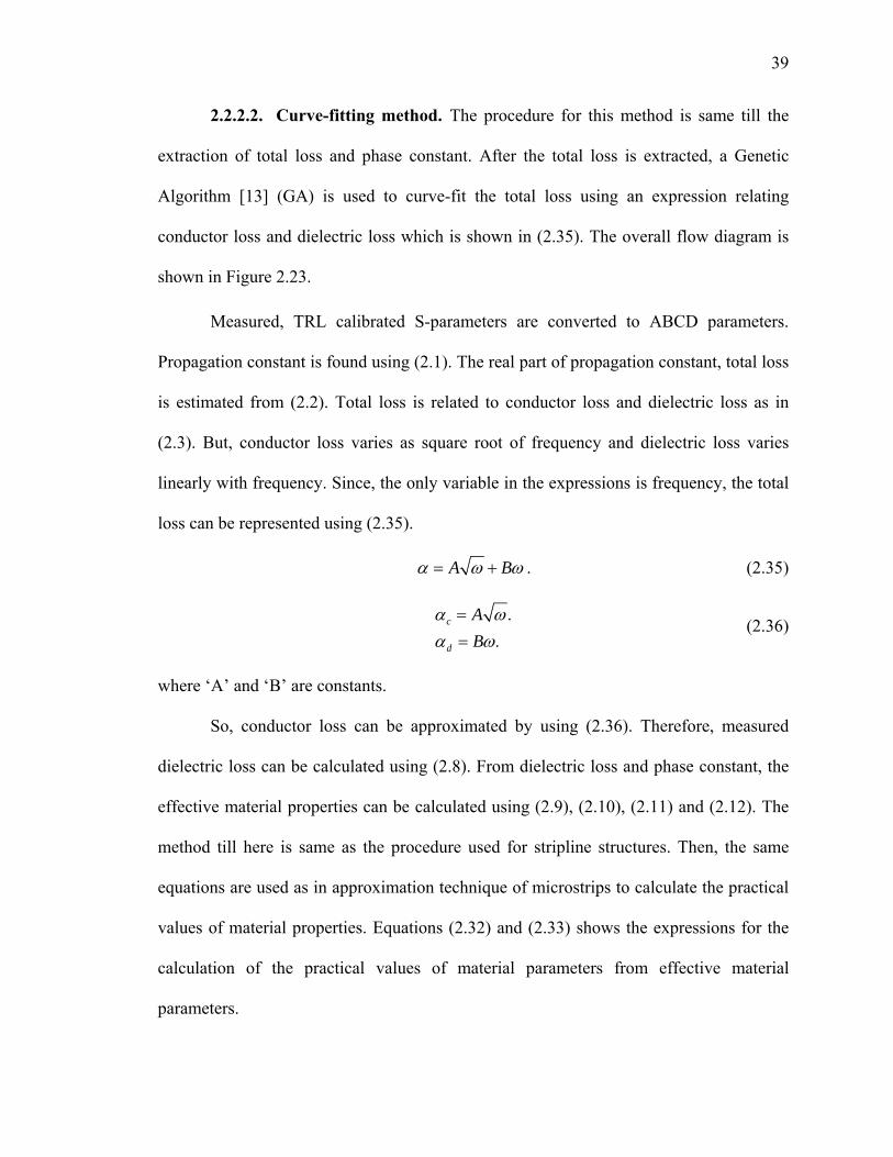
2.2.2.2. Curve-fitting method. The procedure for this method is same till the
extraction of total loss and phase constant. After the total loss is extracted, a Genetic
Algorithm [13] (GA) is used to curve-fit the total loss using an expression relating
conductor loss and dielectric loss which is shown in (2.35). The overall flow diagram is
shown in Figure 2.23.
Measured, TRL calibrated S-parameters are converted to ABCD parameters.
Propagation constant is found using (2.1). The real part of propagation constant, total loss
is estimated from (2.2). Total loss is related to conductor loss and dielectric loss as in
(2.3). But, conductor loss varies as square root of frequency and dielectric loss varies
linearly with frequency. Since, the only variable in the expressions is frequency, the total
loss can be represented using (2.35).
A Bα ω ω= + . (2.35)
..
c
d
AB
α ωα ω
=
= (2.36)
where ‘A’ and ‘B’ are constants.
So, conductor loss can be approximated by using (2.36). Therefore, measured
dielectric loss can be calculated using (2.8). From dielectric loss and phase constant, the
effective material properties can be calculated using (2.9), (2.10), (2.11) and (2.12). The
method till here is same as the procedure used for stripline structures. Then, the same
equations are used as in approximation technique of microstrips to calculate the practical
values of material properties. Equations (2.32) and (2.33) shows the expressions for the
calculation of the practical values of material parameters from effective material
parameters.
40
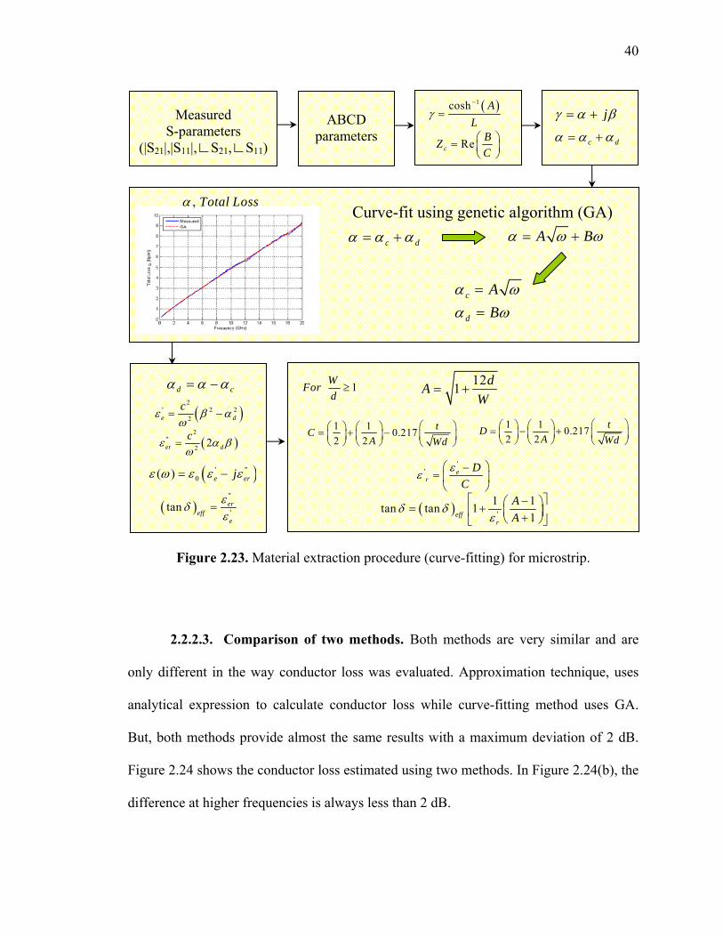
Figure 2.23. Material extraction procedure (curve-fitting) for microstrip.
2.2.2.3. Comparison of two methods. Both methods are very similar and are
only different in the way conductor loss was evaluated. Approximation technique, uses
analytical expression to calculate conductor loss while curve-fitting method uses GA.
But, both methods provide almost the same results with a maximum deviation of 2 dB.
Figure 2.24 shows the conductor loss estimated using two methods. In Figure 2.24(b), the
difference at higher frequencies is always less than 2 dB.
( )1cosh AL
γ−
=ABCD parameters Rec
BZC
⎛ ⎞= ⎜ ⎟⎝ ⎠
c dα α α= +
jγ α β= +Measured S-parameters
(|S21|,|S11|,∟S21,∟S11)
( )2
''2 2er d
cε α βω
=
( )2
' 2 22e d
cε β αω
= −
d cα α α= −
( )' ''0( ) e erjε ω ε ε ε= −
( )''
'tan ereff
e
εδε
=
1WFord
≥ 121 dAW
= +
'' er
DC
εε⎛ ⎞−
= ⎜ ⎟⎝ ⎠
1 1 0.2172 2
tCA Wd
⎛ ⎞⎛ ⎞ ⎛ ⎞= + −⎜ ⎟ ⎜ ⎟ ⎜ ⎟⎝ ⎠ ⎝ ⎠ ⎝ ⎠
1 1 0.2172 2
tDA Wd
⎛ ⎞⎛ ⎞ ⎛ ⎞= − +⎜ ⎟ ⎜ ⎟ ⎜ ⎟⎝ ⎠ ⎝ ⎠ ⎝ ⎠
( ) '
1 1tan tan 11eff
r
AA
δ δε
⎡ ⎤−⎛ ⎞= +⎢ ⎥⎜ ⎟+⎝ ⎠⎣ ⎦
, Total LossαCurve-fit using genetic algorithm (GA)
c dα α α= + A Bα ω ω= +
c
d
AB
α ωα ω
=
=
41
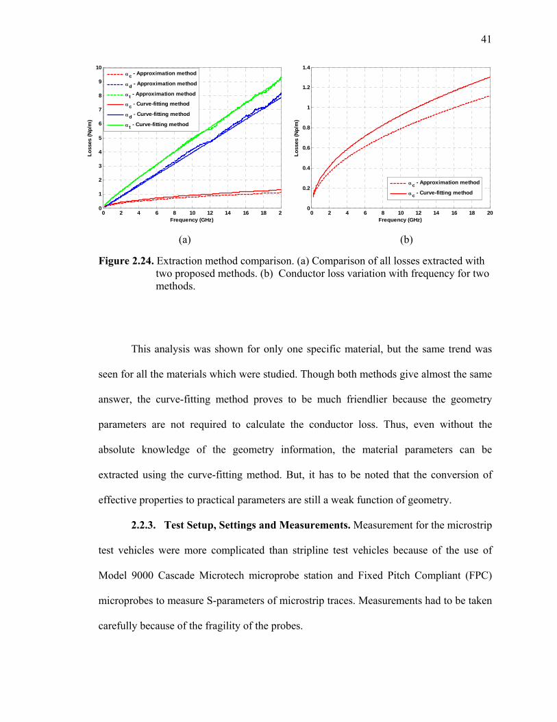
Figure 2.24. Extraction method comparison. (a) Comparison of all losses extracted with two proposed methods. (b) Conductor loss variation with frequency for two methods.
This analysis was shown for only one specific material, but the same trend was
seen for all the materials which were studied. Though both methods give almost the same
answer, the curve-fitting method proves to be much friendlier because the geometry
parameters are not required to calculate the conductor loss. Thus, even without the
absolute knowledge of the geometry information, the material parameters can be
extracted using the curve-fitting method. But, it has to be noted that the conversion of
effective properties to practical parameters are still a weak function of geometry.
2.2.3. Test Setup, Settings and Measurements. Measurement for the microstrip
test vehicles were more complicated than stripline test vehicles because of the use of
Model 9000 Cascade Microtech microprobe station and Fixed Pitch Compliant (FPC)
microprobes to measure S-parameters of microstrip traces. Measurements had to be taken
carefully because of the fragility of the probes.
(a) (b)
0 2 4 6 8 10 12 14 16 18 200
1
2
3
4
5
6
7
8
9
10
Frequency (GHz)
Loss
es (N
p/m
)
αc - Approximation method
αd - Approximation method
α t - Approximation method
αc - Curve-fitting method
αd - Curve-fitting method
α t - Curve-fitting method
0 2 4 6 8 10 12 14 16 18 200
0.2
0.4
0.6
0.8
1
1.2
1.4
Frequency (GHz)
Loss
es (N
p/m
)
αc - Approximation method
αc - Curve-fitting method
42
The overall test setup consisted of a HP8270D network analyzer, high precision
microwave cables, 1000μm pitch Cascade microprobes on the microprobe station, and the
microstrip test board. Figure 2.25 shows the real time test setup used for measuring S-
parameters of microstrip traces.
Figure 2.25. Test setup for microstrip test board measurement.
The monitor was used to display the microscope’s view to better observe the
landing pad and probe tips. High precision cables were connected to the VNA and to the
two microprobes. The microprobes were mounted on a Model 9000 Cascade microprobe
station. The test board was fixed on the probe station with suction control. Microscope
was turned ON and the image was viewed through the monitor. The board was adjusted
so that the pad was clearly visible on the screen. The probes were adjusted with
horizontal x and y knobs to position the probe right above the pad. Then the vertical knob
was adjusted so that the probe touches the pad. Utmost care had to be given while
VNA HP 8720ES
(50MHz-20GHz) Microprobe Station
Model 9000
Cascade Microtech
Precision Cables Low loss microwave
cables
43
bringing the probe down to made sure that the probe touches the pad. After it touches the
pad, the probe slides forward (skating). Enough pressure had to be given to the probe so
that it slides at least 0.1mm forward to make proper contact. This had to be done on both
sides of the trace. Once properly connected, calibration and measurements were done.
TRL calibration procedure explained in Section 2.1.3 was used for microstrip test
board also. The frequency range of interest for this study was 200 MHz – 20 GHz. But,
this frequency range was split into three different sections and the corresponding traces in
the test board were used for calibration. Each frequency range has to be calibrated
separately because each involves different instrument settings. Once calibrated, the
instrument settings and calibration data were stored in the VNA for further
measurements. For the first frequency range 200 MHz – 930 MHz, the trace SL1 in
Figure 2.19 was used as calibration “Line”. For second frequency range 930 MHz – 4.3
GHz, the trace SL2 was used as “Line” calibration standard and for the third frequency
range 4.3 GHz – 20 GHz, SL3 was used as “Line” calibration standard.
Each frequency range was calibrated separately with different number of points.
VNA was set to auto power mode. The first frequency range was set from 200 MHz –
930 MHz with 201 points. The number of averages was set over 16 averages. This was
used to reduce the noise in the calibration and measurements. Setting the averages would
also set the return loss of the “Thru” standard to as low as -60 dB. First “Thru” standard
called ST in Figure 2.19 was connected to VNA for calibration, then “Open” standard
called SO was connected for calibration. Then “Line” standard SL1 was connected for
calibrating the first frequency range. Isolation was omitted. Once all the standards were
measured, the calibration was finished and it was saved for actual measurements.
44
Similarly, calibrations were done for second frequency range, 930 Mhz – 4.3 GHz with
801 points using the “Line” standard SL2. Calibration was also done for third frequency
range 4.3 GHz – 20 GHz with 1601 points using “Line” standard SL3. Once all three
frequency ranges were calibrated, measurements were taken on ST1 and ST2. These were
very long traces which cannot be viewed through the microscope in the probe station.
External microscopes had to be used to view the pads.
The microprobes used for these measurements were 1000μm pitch probes. Two
different probes had to be used because of the Ground-Signal configuration of the pad
design. Figure 2.26 shows the pads and the corresponding probe configurations used on
both sides. The pads for the ground vias were located at the same side of the trace. This
required the use of two different configurations of probes.
Figure 2.26. View of pads configuration and probe configuration at the edge of traces on
the test boards.
Gnd
Signal
Gnd
Signal
Probe1 Cascade Microtech
FPC-GS-1000
Probe2 Cascade Microtech
FPC-SG-1000
45
The microprobes used were FPC-GS-1000 and FPC-SG-1000 from Cascade
Microtech. These probes were very fragile and utmost care had to be taken for reuse.
Pressurized air was used to clean the tips of the probe after measurements. This removed
the copper debris accumulated at the tips after several measurement cycles. The pads are
clearly visible on Figure 2.26. The Ground-Signal configuration is different on both
sides. Each probe could only handle a certain number of landing procedures and
eventually the tips break off. The probes were very costly and hard to maintain. Other
disadvantage of the 1000μm probe was its large tip inductance. TDR measurements were
taken to see the impedance of the traces. Figure 2.27 shows the large peak on both sides
of the trace showing its large tip inductance. But, with our calibration technique, these
effects are taken off in part, assuming that both probes are identical.
Figure 2.27. TDR measurements on the traces showing the large inductance on both
sides of the trace associated with the tips.
19.5 20 20.5 21 21.5 22 22.5
51
52
53
54
55
56
57
58
59
60
61
TDR Measurements on a microstrip test board
Time(ns)
Impe
danc
e(Ω
)
cableVSTVSL3VSL2VSL1VST1VST2
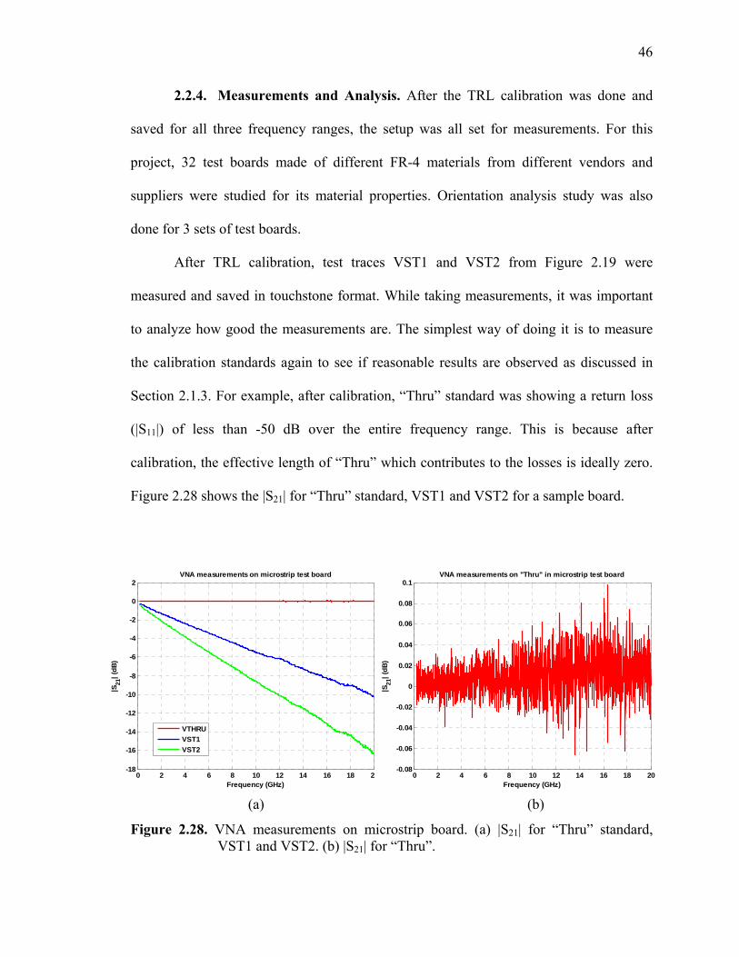
46
2.2.4. Measurements and Analysis. After the TRL calibration was done and
saved for all three frequency ranges, the setup was all set for measurements. For this
project, 32 test boards made of different FR-4 materials from different vendors and
suppliers were studied for its material properties. Orientation analysis study was also
done for 3 sets of test boards.
After TRL calibration, test traces VST1 and VST2 from Figure 2.19 were
measured and saved in touchstone format. While taking measurements, it was important
to analyze how good the measurements are. The simplest way of doing it is to measure
the calibration standards again to see if reasonable results are observed as discussed in
Section 2.1.3. For example, after calibration, “Thru” standard was showing a return loss
(|S11|) of less than -50 dB over the entire frequency range. This is because after
calibration, the effective length of “Thru” which contributes to the losses is ideally zero.
Figure 2.28 shows the |S21| for “Thru” standard, VST1 and VST2 for a sample board.
Figure 2.28. VNA measurements on microstrip board. (a) |S21| for “Thru” standard,
VST1 and VST2. (b) |S21| for “Thru”.
(a) (b)
0 2 4 6 8 10 12 14 16 18 20-18
-16
-14
-12
-10
-8
-6
-4
-2
0
2VNA measurements on microstrip test board
Frequency (GHz)
|S21
| (dB
)
VTHRUVST1VST2
0 2 4 6 8 10 12 14 16 18 20-0.08
-0.06
-0.04
-0.02
0
0.02
0.04
0.06
0.08
0.1VNA measurements on "Thru" in microstrip test board
Frequency (GHz)
|S21
| (dB
)
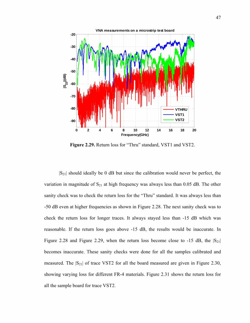
47
Figure 2.29. Return loss for “Thru” standard, VST1 and VST2.
|S21| should ideally be 0 dB but since the calibration would never be perfect, the
variation in magnitude of S21 at high frequency was always less than 0.05 dB. The other
sanity check was to check the return loss for the “Thru” standard. It was always less than
-50 dB even at higher frequencies as shown in Figure 2.28. The next sanity check was to
check the return loss for longer traces. It always stayed less than -15 dB which was
reasonable. If the return loss goes above -15 dB, the results would be inaccurate. In
Figure 2.28 and Figure 2.29, when the return loss become close to -15 dB, the |S21|
becomes inaccurate. These sanity checks were done for all the samples calibrated and
measured. The |S21| of trace VST2 for all the board measured are given in Figure 2.30,
showing varying loss for different FR-4 materials. Figure 2.31 shows the return loss for
all the sample board for trace VST2.
0 2 4 6 8 10 12 14 16 18 20
-90
-80
-70
-60
-50
-40
-30
-20VNA measurements on a microstrip test board
Frequency(GHz)
|S22
|(dB
)
VTHRUVST1VST2
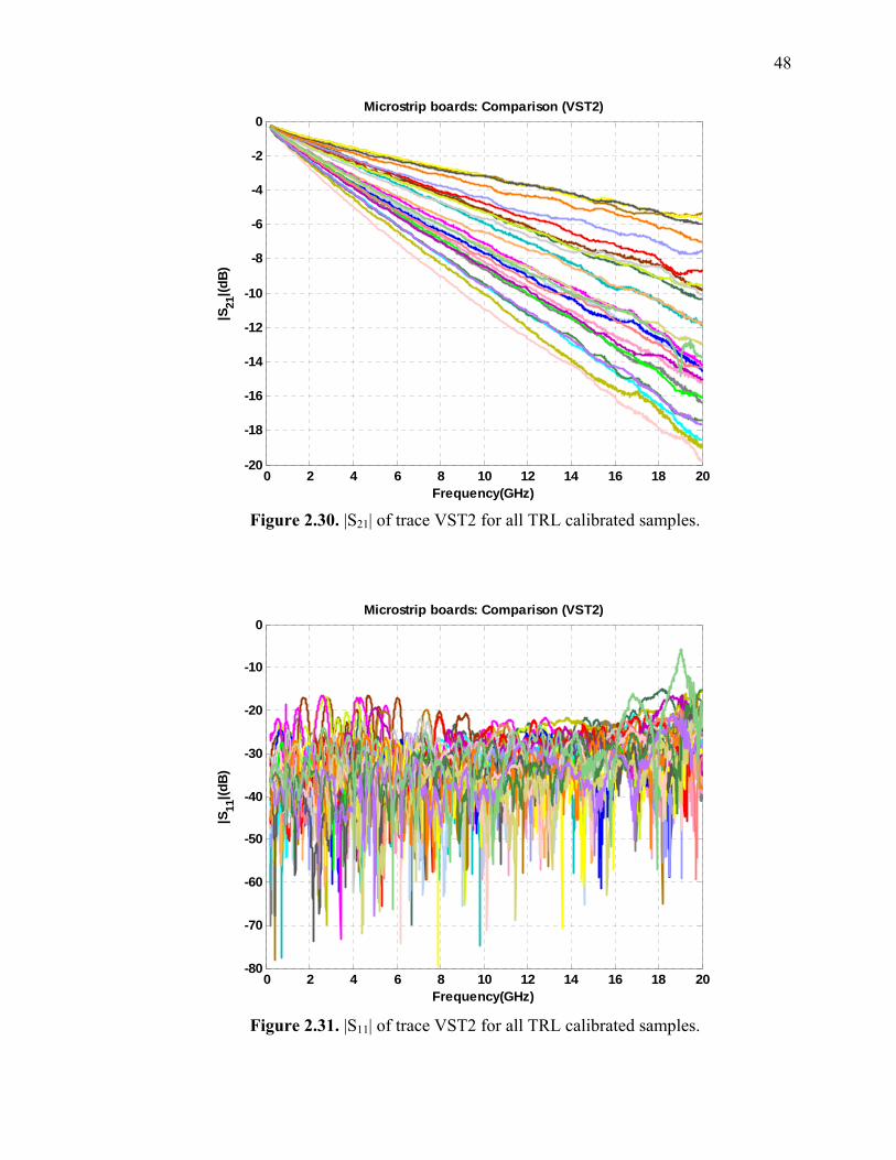
48
Figure 2.30. |S21| of trace VST2 for all TRL calibrated samples.
Figure 2.31. |S11| of trace VST2 for all TRL calibrated samples.
0 2 4 6 8 10 12 14 16 18 20-20
-18
-16
-14
-12
-10
-8
-6
-4
-2
0Microstrip boards: Comparison (VST2)
Frequency(GHz)
|S21
|(dB
)
0 2 4 6 8 10 12 14 16 18 20-80
-70
-60
-50
-40
-30
-20
-10
0Microstrip boards: Comparison (VST2)
Frequency(GHz)
|S11
|(dB
)
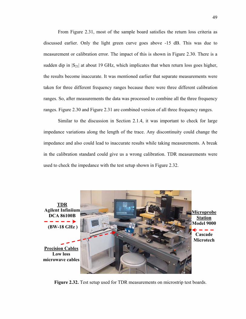
49
From Figure 2.31, most of the sample board satisfies the return loss criteria as
discussed earlier. Only the light green curve goes above -15 dB. This was due to
measurement or calibration error. The impact of this is shown in Figure 2.30. There is a
sudden dip in |S21| at about 19 GHz, which implicates that when return loss goes higher,
the results become inaccurate. It was mentioned earlier that separate measurements were
taken for three different frequency ranges because there were three different calibration
ranges. So, after measurements the data was processed to combine all the three frequency
ranges. Figure 2.30 and Figure 2.31 are combined version of all three frequency ranges.
Similar to the discussion in Section 2.1.4, it was important to check for large
impedance variations along the length of the trace. Any discontinuity could change the
impedance and also could lead to inaccurate results while taking measurements. A break
in the calibration standard could give us a wrong calibration. TDR measurements were
used to check the impedance with the test setup shown in Figure 2.32.
Figure 2.32. Test setup used for TDR measurements on microstrip test boards.
TDR Agilent Infiniium
DCA 86100B
(BW-18 GHz )
Microprobe Station
Model 9000
Cascade Microtech
Precision Cables Low loss
microwave cables

50
Figure 2.33 shows a typical TDR measurement from one of the sample boards. It
was important to measure the continuity of all the traces in the sample board. This is
similar to the setup shown in Figure 2.13. The only difference being that, the traces were
probed using microprobes instead of connectors. All samples were analyzed using TDR
measurements and were proved to be nearly 50Ω.
Figure 2.33. Impedance measurements on microstrip board. (a) TDR Impedance measurement along the trace length (b) Inductive connector discontinuity (c) Enlarged view of impedance variation along the trace.
19.8 19.85 19.9 19.95 20 20.05
51
52
53
54
55
56
57
58
59
60
61
TDR measurements on a microstrip test board
Time (ns)
Impe
danc
e ( Ω
)
cableVSTVSL3VSL2VSL1VST1VST2
19.5 20 20.5 21 21.5 22 22.5
50
52
54
56
58
60
TDR measurements on a microstrip test board
Time (ns)
Impe
danc
e ( Ω
)
cableVSTVSL3VSL2VSL1VST1VST2
19.5 20 20.5 21 21.5 22 22.5 23 23.5 240
10
20
30
40
50
60
TDR measurements on a microstrip test board
Time (ns)
Impe
danc
e ( Ω
)
cableVSTVSL3VSL2VSL1VST1VST2
(a)
(b) (c)
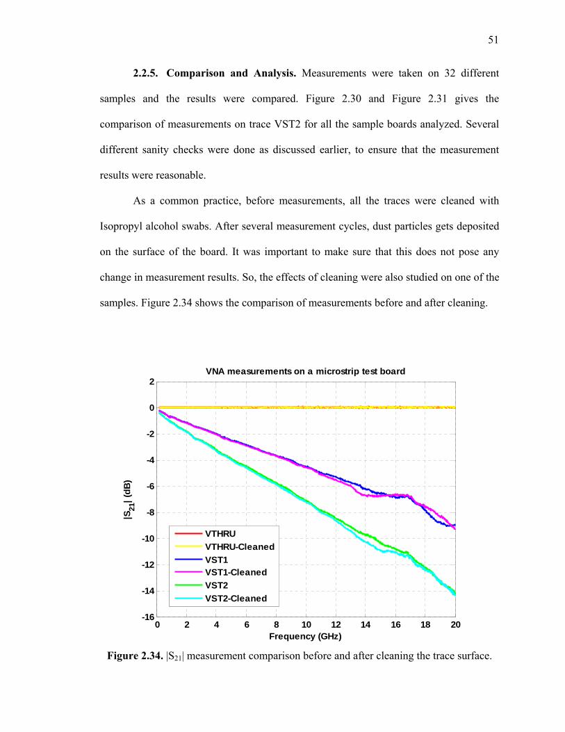
51
2.2.5. Comparison and Analysis. Measurements were taken on 32 different
samples and the results were compared. Figure 2.30 and Figure 2.31 gives the
comparison of measurements on trace VST2 for all the sample boards analyzed. Several
different sanity checks were done as discussed earlier, to ensure that the measurement
results were reasonable.
As a common practice, before measurements, all the traces were cleaned with
Isopropyl alcohol swabs. After several measurement cycles, dust particles gets deposited
on the surface of the board. It was important to make sure that this does not pose any
change in measurement results. So, the effects of cleaning were also studied on one of the
samples. Figure 2.34 shows the comparison of measurements before and after cleaning.
0 2 4 6 8 10 12 14 16 18 20-16
-14
-12
-10
-8
-6
-4
-2
0
2VNA measurements on a microstrip test board
Frequency (GHz)
|S21
| (dB
)
VTHRUVTHRU-CleanedVST1VST1-CleanedVST2VST2-Cleaned
Figure 2.34. |S21| measurement comparison before and after cleaning the trace surface.
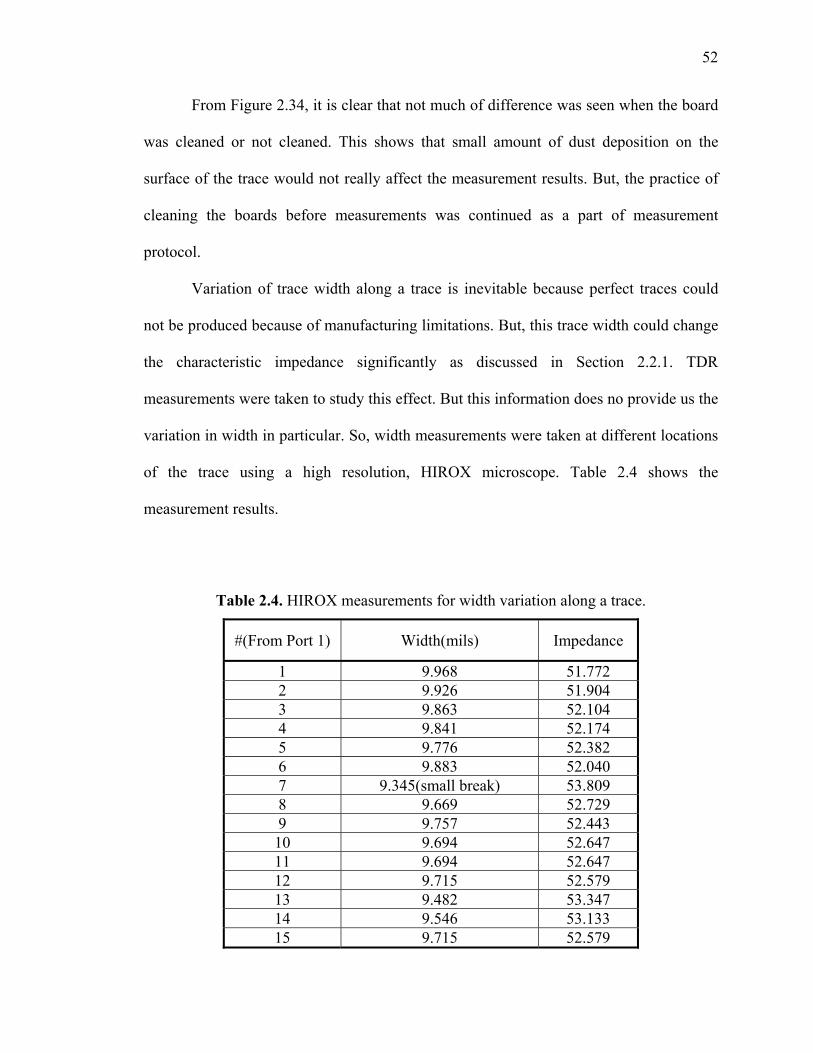
52
From Figure 2.34, it is clear that not much of difference was seen when the board
was cleaned or not cleaned. This shows that small amount of dust deposition on the
surface of the trace would not really affect the measurement results. But, the practice of
cleaning the boards before measurements was continued as a part of measurement
protocol.
Variation of trace width along a trace is inevitable because perfect traces could
not be produced because of manufacturing limitations. But, this trace width could change
the characteristic impedance significantly as discussed in Section 2.2.1. TDR
measurements were taken to study this effect. But this information does no provide us the
variation in width in particular. So, width measurements were taken at different locations
of the trace using a high resolution, HIROX microscope. Table 2.4 shows the
measurement results.
Table 2.4. HIROX measurements for width variation along a trace.
#(From Port 1) Width(mils) Impedance
1 9.968 51.772 2 9.926 51.904 3 9.863 52.104 4 9.841 52.174 5 9.776 52.382 6 9.883 52.040 7 9.345(small break) 53.809 8 9.669 52.729 9 9.757 52.443 10 9.694 52.647 11 9.694 52.647 12 9.715 52.579 13 9.482 53.347 14 9.546 53.133 15 9.715 52.579
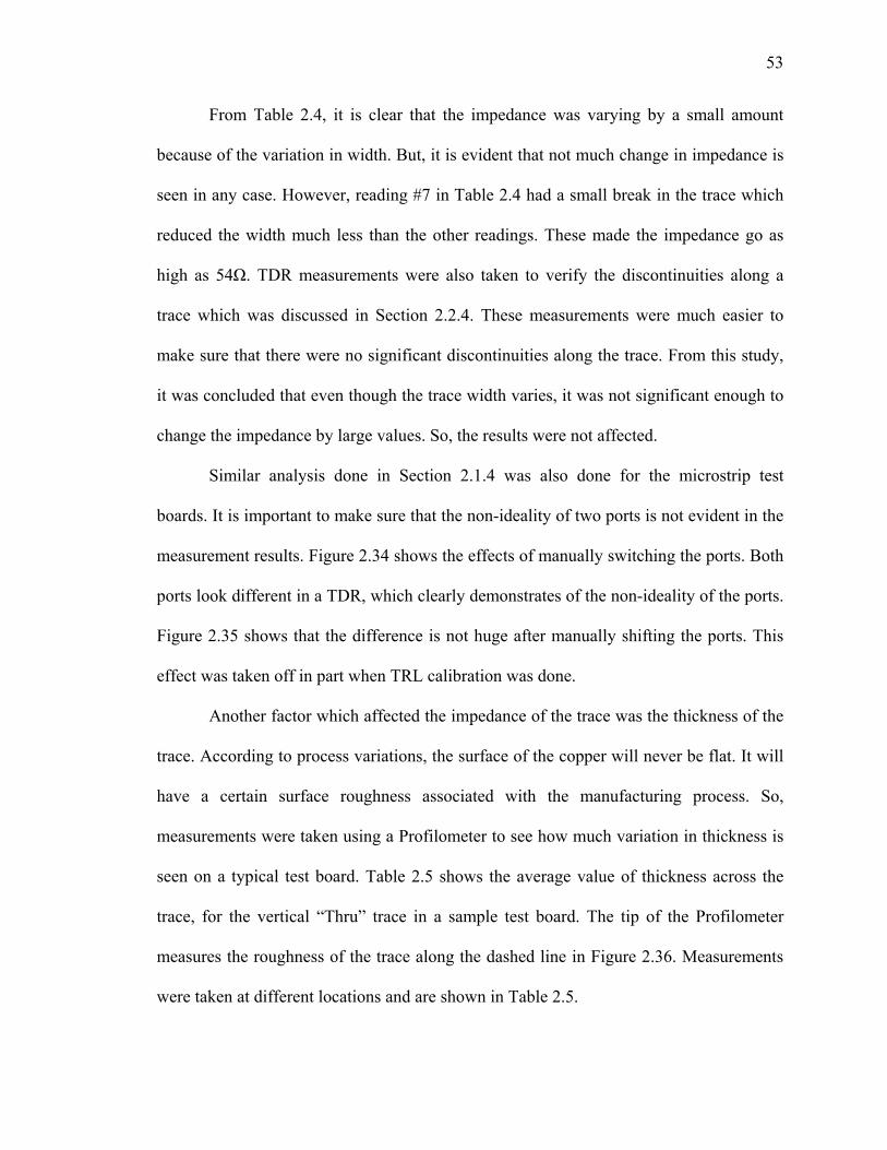
53
From Table 2.4, it is clear that the impedance was varying by a small amount
because of the variation in width. But, it is evident that not much change in impedance is
seen in any case. However, reading #7 in Table 2.4 had a small break in the trace which
reduced the width much less than the other readings. These made the impedance go as
high as 54Ω. TDR measurements were also taken to verify the discontinuities along a
trace which was discussed in Section 2.2.4. These measurements were much easier to
make sure that there were no significant discontinuities along the trace. From this study,
it was concluded that even though the trace width varies, it was not significant enough to
change the impedance by large values. So, the results were not affected.
Similar analysis done in Section 2.1.4 was also done for the microstrip test
boards. It is important to make sure that the non-ideality of two ports is not evident in the
measurement results. Figure 2.34 shows the effects of manually switching the ports. Both
ports look different in a TDR, which clearly demonstrates of the non-ideality of the ports.
Figure 2.35 shows that the difference is not huge after manually shifting the ports. This
effect was taken off in part when TRL calibration was done.
Another factor which affected the impedance of the trace was the thickness of the
trace. According to process variations, the surface of the copper will never be flat. It will
have a certain surface roughness associated with the manufacturing process. So,
measurements were taken using a Profilometer to see how much variation in thickness is
seen on a typical test board. Table 2.5 shows the average value of thickness across the
trace, for the vertical “Thru” trace in a sample test board. The tip of the Profilometer
measures the roughness of the trace along the dashed line in Figure 2.36. Measurements
were taken at different locations and are shown in Table 2.5.
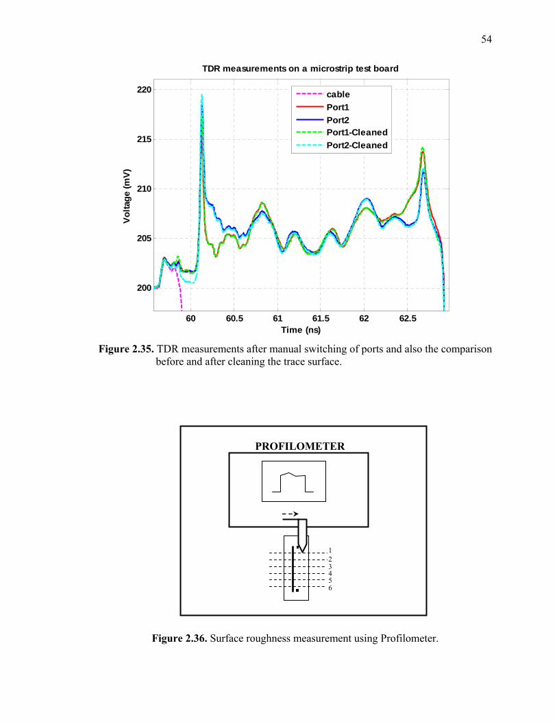
54
Figure 2.35. TDR measurements after manual switching of ports and also the comparison
before and after cleaning the trace surface.
Figure 2.36. Surface roughness measurement using Profilometer.
1 2 3 4 5 6
PROFILOMETER
60 60.5 61 61.5 62 62.5
200
205
210
215
220
TDR measurements on a microstrip test board
Time (ns)
Vol
tage
(mV)
cablePort1Port2Port1-CleanedPort2-Cleaned
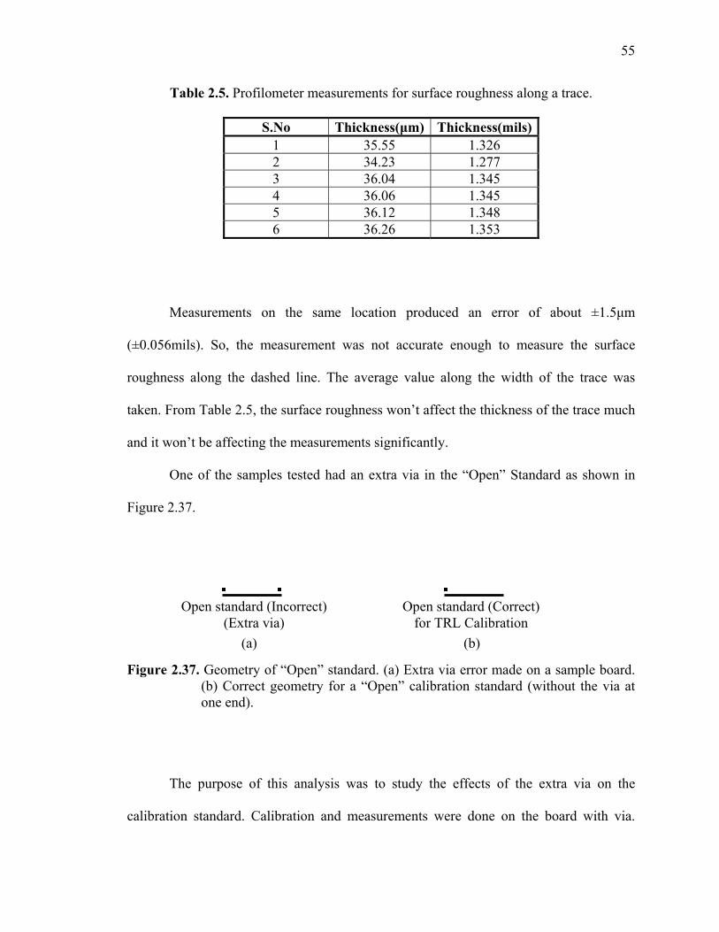
55
Table 2.5. Profilometer measurements for surface roughness along a trace.
S.No Thickness(μm) Thickness(mils) 1 35.55 1.326 2 34.23 1.277 3 36.04 1.345 4 36.06 1.345 5 36.12 1.348 6 36.26 1.353
Measurements on the same location produced an error of about ±1.5μm
(±0.056mils). So, the measurement was not accurate enough to measure the surface
roughness along the dashed line. The average value along the width of the trace was
taken. From Table 2.5, the surface roughness won’t affect the thickness of the trace much
and it won’t be affecting the measurements significantly.
One of the samples tested had an extra via in the “Open” Standard as shown in
Figure 2.37.
Figure 2.37. Geometry of “Open” standard. (a) Extra via error made on a sample board.
(b) Correct geometry for a “Open” calibration standard (without the via at one end).
The purpose of this analysis was to study the effects of the extra via on the
calibration standard. Calibration and measurements were done on the board with via.
Open standard (Incorrect) (Extra via)
Open standard (Correct) for TRL Calibration
(a) (b)
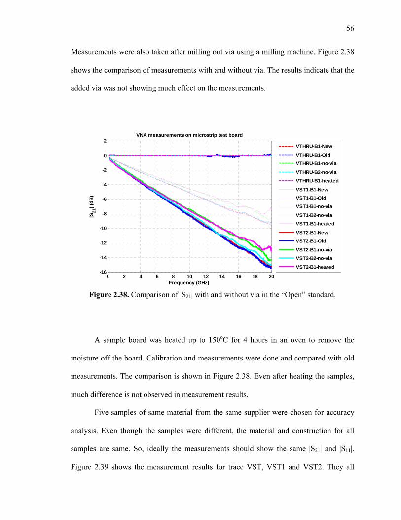
56
Measurements were also taken after milling out via using a milling machine. Figure 2.38
shows the comparison of measurements with and without via. The results indicate that the
added via was not showing much effect on the measurements.
0 2 4 6 8 10 12 14 16 18 20-16
-14
-12
-10
-8
-6
-4
-2
0
2VNA measurements on microstrip test board
Frequency (GHz)
|S21
| (dB
)
VTHRU-B1-New
VTHRU-B1-OldVTHRU-B1-no-via
VTHRU-B2-no-viaVTHRU-B1-heated
VST1-B1-NewVST1-B1-OldVST1-B1-no-via
VST1-B2-no-viaVST1-B1-heated
VST2-B1-NewVST2-B1-Old
VST2-B1-no-viaVST2-B2-no-via
VST2-B1-heated
Figure 2.38. Comparison of |S21| with and without via in the “Open” standard.
A sample board was heated up to 150oC for 4 hours in an oven to remove the
moisture off the board. Calibration and measurements were done and compared with old
measurements. The comparison is shown in Figure 2.38. Even after heating the samples,
much difference is not observed in measurement results.
Five samples of same material from the same supplier were chosen for accuracy
analysis. Even though the samples were different, the material and construction for all
samples are same. So, ideally the measurements should show the same |S21| and |S11|.
Figure 2.39 shows the measurement results for trace VST, VST1 and VST2. They all
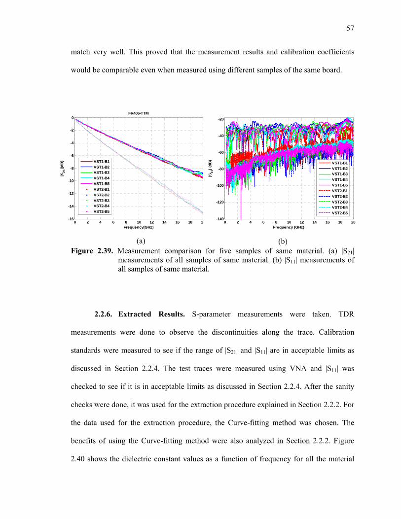
57
match very well. This proved that the measurement results and calibration coefficients
would be comparable even when measured using different samples of the same board.
Figure 2.39. Measurement comparison for five samples of same material. (a) |S21|
measurements of all samples of same material. (b) |S11| measurements of all samples of same material.
2.2.6. Extracted Results. S-parameter measurements were taken. TDR
measurements were done to observe the discontinuities along the trace. Calibration
standards were measured to see if the range of |S21| and |S11| are in acceptable limits as
discussed in Section 2.2.4. The test traces were measured using VNA and |S11| was
checked to see if it is in acceptable limits as discussed in Section 2.2.4. After the sanity
checks were done, it was used for the extraction procedure explained in Section 2.2.2. For
the data used for the extraction procedure, the Curve-fitting method was chosen. The
benefits of using the Curve-fitting method were also analyzed in Section 2.2.2. Figure
2.40 shows the dielectric constant values as a function of frequency for all the material
(b)(a)
0 2 4 6 8 10 12 14 16 18 20-16
-14
-12
-10
-8
-6
-4
-2
0FR406-TTM
Frequency(GHz)
|S21
|(dB
)
VST1-B1VST1-B2VST1-B3VST1-B4VST1-B5VST2-B1VST2-B2VST2-B3VST2-B4VST2-B5
0 2 4 6 8 10 12 14 16 18 20-140
-120
-100
-80
-60
-40
-20
Frequency (GHz)
|S11
| (dB
)
VST1-B1VST1-B2VST1-B3VST1-B4VST1-B5VST2-B1VST2-B2VST2-B3VST2-B4VST2-B5
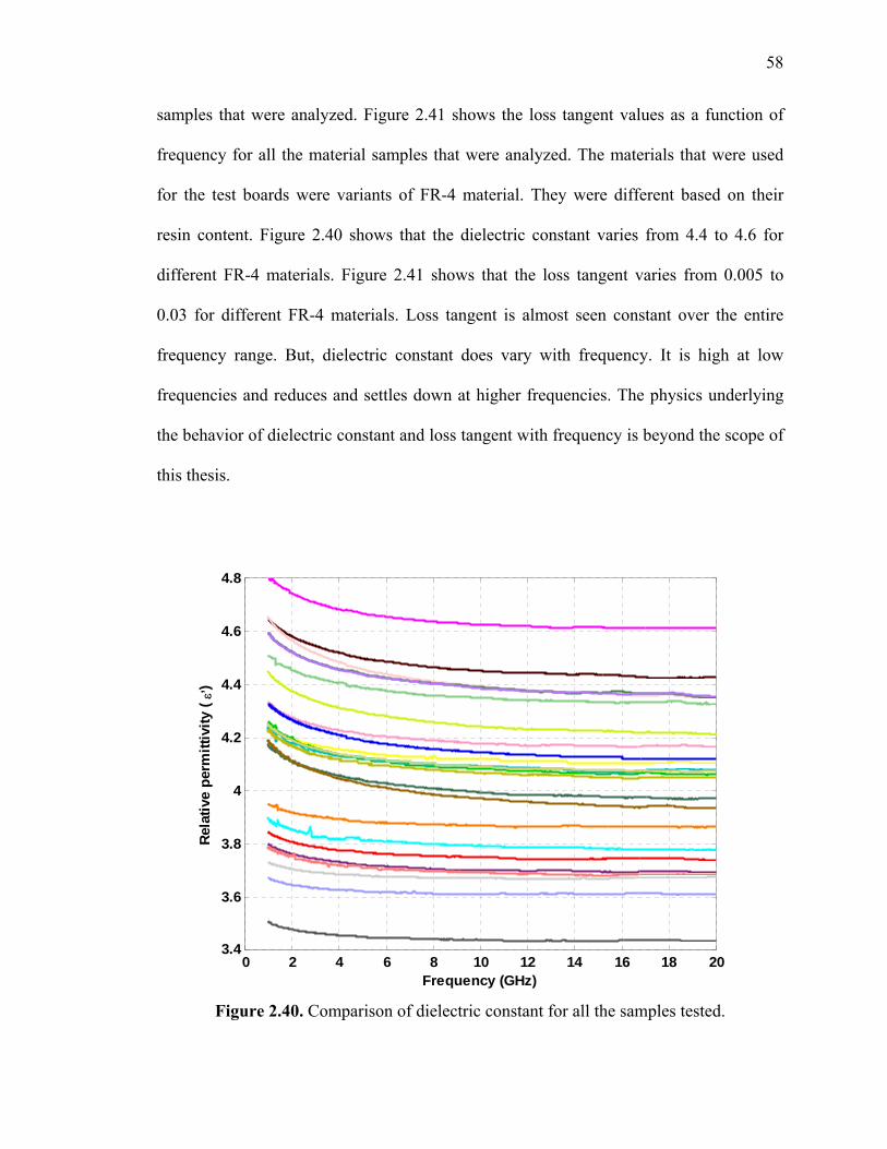
58
samples that were analyzed. Figure 2.41 shows the loss tangent values as a function of
frequency for all the material samples that were analyzed. The materials that were used
for the test boards were variants of FR-4 material. They were different based on their
resin content. Figure 2.40 shows that the dielectric constant varies from 4.4 to 4.6 for
different FR-4 materials. Figure 2.41 shows that the loss tangent varies from 0.005 to
0.03 for different FR-4 materials. Loss tangent is almost seen constant over the entire
frequency range. But, dielectric constant does vary with frequency. It is high at low
frequencies and reduces and settles down at higher frequencies. The physics underlying
the behavior of dielectric constant and loss tangent with frequency is beyond the scope of
this thesis.
0 2 4 6 8 10 12 14 16 18 203.4
3.6
3.8
4
4.2
4.4
4.6
4.8
Frequency (GHz)
Rela
tive
perm
ittiv
ity (ε, )
Figure 2.40. Comparison of dielectric constant for all the samples tested.
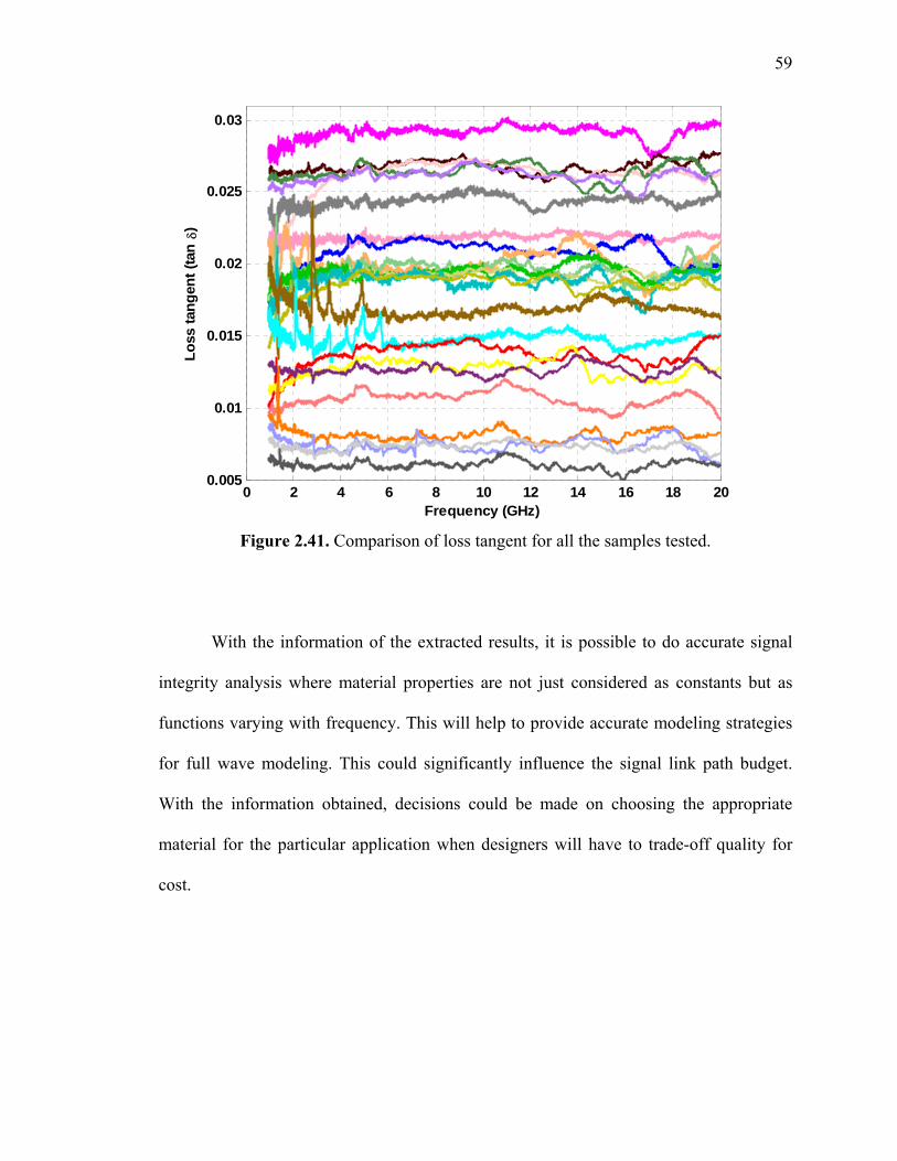
59
Figure 2.41. Comparison of loss tangent for all the samples tested.
With the information of the extracted results, it is possible to do accurate signal
integrity analysis where material properties are not just considered as constants but as
functions varying with frequency. This will help to provide accurate modeling strategies
for full wave modeling. This could significantly influence the signal link path budget.
With the information obtained, decisions could be made on choosing the appropriate
material for the particular application when designers will have to trade-off quality for
cost.
0 2 4 6 8 10 12 14 16 18 200.005
0.01
0.015
0.02
0.025
0.03
Frequency (GHz)
Loss
tang
ent (
tan δ)

60
3. ROOT IMPULSE ENERGY (RIE) LOSS Loss characterization is always preferred to be done in frequency domain because
the loss information is embodied in information rich S-parameters from a Vector
Network Analyzer (VNA). Also, dielectric properties of a material are frequency
dependant parameters. But, VNA is a very costly equipment and measurement procedure
is complicated to be used in board houses for quick measurements. Board houses which
manufacture such boards require an easy robust technique to characterize losses so that
they can provide a good estimate of the losses to its supplier.
Time Domain Reflectometer (TDR), is a time domain equipment which sends out
a pulse to a device under test and measures the reflected signal. It is less costly when
compared to VNA and could be easily used in board houses for measurements. So, this is
the motivation of the technique discussed in this Section is to build a time domain
technique to characterize losses easily and produce a single valued number for losses
which is representative of the entire frequency range under consideration. TDR losses
have shown correlation to VNA measurements, but have a much simpler representation
which is more suitable to specification and ease of measurement.
The observed edge of a TDR waveform is related to energy lost in the
transmission line attached to the TDR unit. The intent of Root Impulse Energy (RIE) loss
is to represent losses as a single valued energy loss of a transmission line on a printed
circuit board (PCB) which is representative of its losses as a function of frequency. A
step signal is injected into the transmission line. Energy is lost as the wave travels
through the transmission line. The loss characteristics of a transmission line can be

61
determined by comparing the RIE of the injected wave to the RIE of the reflected wave.
This is called RIE loss.
First, a time domain technique is defined in this Section and then a frequency
domain technique is analyzed, both analytical and measurement wise, on a stripline
structure. This was done to compare the RIE loss numbers with the standard VNA
measurements and correlate to see how well they agree.
3.1. TIME DOMAIN CHARACTERIZATION
One of Newton’s fundamental laws of physics states that “energy must be
conserved.” This is true for systems viewed in the both the time and frequency domain
because, frequency domain is nothing but a mathematical manipulation of numbers to
allow easier solutions to everyday problems. To satisfy conservation, the energy can be
transmitted, reflected, radiated, or absorbed and turned into heat. The energy not
delivered to the load is considered lost. The loss can be measured as a ratio of received
(Rx) energy to the injected (In) energy.
Insertion loss is a parameter that is roughly the square root of the ratio of received
energy to injected energy and is a function of frequency. Since loss is not a single value,
it is difficult and complicated to specify it, in terms of limits. The purpose of the RIE
method is to define a single energy loss value as a quality factor. Insertion loss, S21 is,
21rx
in
VSV
≈ . (3.1)
where the received and injected voltages are functions of frequency. The purpose of this
method is to define and utilize a single energy loss value, called the Root Impulse Energy
(RIE) loss.

62
From an electrical perspective, energy is simply product of voltage, current, and
time. Considering that the measurement equipment source impedance and load
impedance is ‘R’, Ohm’s law reveals the following
2VE T
R= ∗ . (3.2)
Total energy is the integral of (3.2) over time.
2( )V tE dt
R= ∗∫ . (3.3)
With (3.3), it is possible to define the RIE loss as a ratio of the received energy with the
injected energy.
2
2
( )
( )
rxrxloss
in in
V t dtERIEE V t dt
∗= =
∗
∫∫
. (3.4)
The above equation (3.4) shows the RIE loss associated with a single trace with
injected and received energies. But, this RIE loss includes losses in edges, cables, launch
pad, and a small section of transmission line. To calculate the energy loss of just the
trace, those effects should be omitted. So, a calibration trace is used, which is only
shorter than the original test trace. Then with the ratio of energies of the test trace to the
calibration trace, it is possible to get the RIE loss number and the unwanted effects are
also eliminated.
An impulse response is required to encompass the widest possible frequency
range so that all the energy associated with the trace is considered. TDR utilizes a step
response. Differentiating the step response would yield an impulse response.
Therefore, considering the impulse response in the RIE loss (in dB) expression,
the following expression (3.5) is derived.
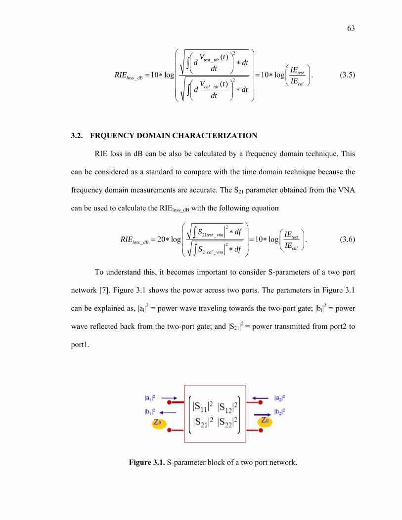
63
2_
_ 2_
( )
10 log 10 log( )
test tdr
testloss dB
calcal tdr
V td dt
dt IERIEIEV t
d dtdt
⎛ ⎞⎛ ⎞⎜ ⎟∗⎜ ⎟⎜ ⎟ ⎛ ⎞⎝ ⎠= ∗ = ∗⎜ ⎟ ⎜ ⎟⎝ ⎠⎜ ⎟⎛ ⎞
∗⎜ ⎟⎜ ⎟⎜ ⎟⎝ ⎠⎝ ⎠
∫
∫. (3.5)
3.2. FRQUENCY DOMAIN CHARACTERIZATION
RIE loss in dB can be also be calculated by a frequency domain technique. This
can be considered as a standard to compare with the time domain technique because the
frequency domain measurements are accurate. The S21 parameter obtained from the VNA
can be used to calculate the RIEloss_dB with the following equation
2
21 _
_ 2
21 _
20 log 10 logtest vna test
loss dBcal
cal vna
S df IERIEIES df
⎛ ⎞∗ ⎛ ⎞⎜ ⎟= ∗ = ∗ ⎜ ⎟⎜ ⎟⎝ ⎠⎜ ⎟∗⎝ ⎠
∫∫
. (3.6)
To understand this, it becomes important to consider S-parameters of a two port
network [7]. Figure 3.1 shows the power across two ports. The parameters in Figure 3.1
can be explained as, |ai|2 = power wave traveling towards the two-port gate; |bi|2 = power
wave reflected back from the two-port gate; and |S21|2 = power transmitted from port2 to
port1.
Figure 3.1. S-parameter block of a two port network.
64
So, the definition of insertion loss S21 is
2
2 2221 22
1
, 0b
S where aa
= = . (3.7)
Therefore, to get the total energy transmitted from port2 to port1 could be obtained by
integrating (3.7) over the entire frequency range.
221E S df= ∗∫ . (3.8)
So, considering the calibration trace and the test trace, the Root Impulse Energy loss is
the ratio of both energies which is shown in the following equation
2
212
21
testloss
cal
S dfRIE
S df
∗=
∗∫∫
. (3.9)
Therefore, the RIE loss in dB can be expressed as
2
21_ 2
21
10 log testloss dB
cal
S dfRIE
S df
⎛ ⎞∗⎜ ⎟= ∗ ⎜ ⎟∗⎜ ⎟⎝ ⎠
∫∫
. (3.10)
(3.10) can also be represented as
2
21
_ 221
10 log 10 logtest test
loss dBcalcal
S df IERIEIES df
⎛ ⎞∗ ⎛ ⎞⎜ ⎟= ∗ = ∗ ⎜ ⎟⎜ ⎟ ⎝ ⎠⎜ ⎟∗⎝ ⎠
∫∫
. (3.11)
3.3. ANALYTICAL EXPRESSION ANALYSIS OF RIE LOSS FOR STRIPLINE
To better understand RIE loss definition, a stripline structure was chosen for
analysis. In later sections, RIE loss would be derived from basic principles of losses in a
transmission line. Losses will be represented in terms of frequency by selecting a
particular configuration of stripline structure.
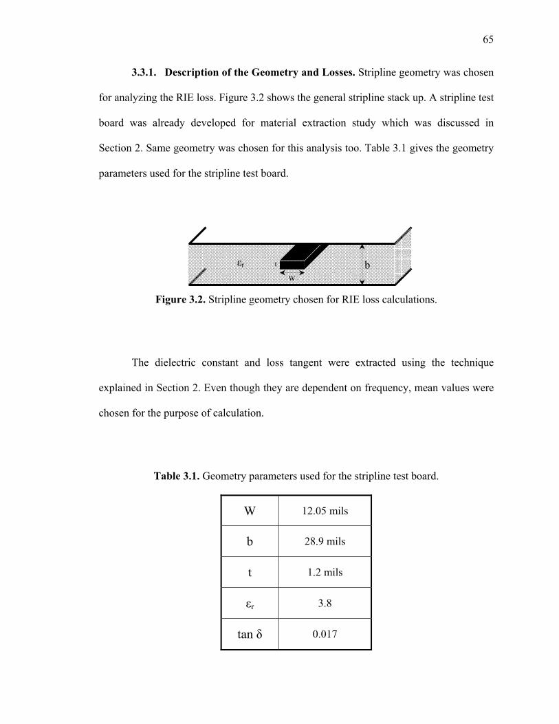
65
3.3.1. Description of the Geometry and Losses. Stripline geometry was chosen
for analyzing the RIE loss. Figure 3.2 shows the general stripline stack up. A stripline test
board was already developed for material extraction study which was discussed in
Section 2. Same geometry was chosen for this analysis too. Table 3.1 gives the geometry
parameters used for the stripline test board.
Figure 3.2. Stripline geometry chosen for RIE loss calculations.
The dielectric constant and loss tangent were extracted using the technique
explained in Section 2. Even though they are dependent on frequency, mean values were
chosen for the purpose of calculation.
Table 3.1. Geometry parameters used for the stripline test board.
W 12.05 mils
b 28.9 mils
t 1.2 mils
εr 3.8
tan δ 0.017
bεr W
t

66
The losses associated with a transmission line were derived from basic voltage
equations. For a transmission line with characteristic impedance, Zo and reflection
coefficient, Γ, the voltage at any length (l) is given by the equation
( ) 0 (1 ) lV l V e γ−= + Γ . (3.12)
Assuming that there is no reflection, (Г) = 0, i.e. when the load is matched, then
0
( ) lV l eV
γ−= . (3.13)
But, the insertion loss can be represented using (3.14).
0
( )V lV
= Transmission coefficient (S21). (3.14)
Therefore, from Equations (3.13) and (3.14)
21( ) lS l e γ−= . (3.15)
where ‘γ’ is the propagation constant and ‘l’ is the length of the transmission line. But,
propagation constant can be represented as
jγ α β= + . (3.16)
where ‘α’ is the total loss of the transmission line and ‘β’ is the phase constant.
Therefore, (3.15) could be written as
( )21( ) j lS l e α β− += . (3.17)
21( ) .l j lS l e eα β− −= . (3.18)
The magnitude of (3.18) is shows as
21( ) lS l e α−= . (3.19)
Squaring (3.19) would provide
2 221( ) lS l e α−= . (3.20)
67
But, attenuation is due to dielectric (αd) and conductor losses (αc). Therefore, the total
attenuation (α) is
d cα α α= + . (3.21)
3.3.2. Attenuation Due to Dielectric Loss (αd). Assuming TEM mode of wave
propagation, the dielectric loss can be expressed the following way[7]
tan2d
k δα = . (3.22)
where ‘k’ is the wave number and is given by
rkc
ω ε= . (3.23)
3.3.3. Attenuation Due to Conductor Loss (αc). For the stripline geometry,
closed form expressions are derived for conductor loss using perturbation method. This is
because conductor loss is just a function of geometry and it depends upon skin effect
losses [7]. Assuming TEM mode of wave propagation, the impedance of the transmission
line can be approximated using the following expression
030
0.441er
bZW b
πε
=+
. (3.24)
where
(3.25)
When designing stripline circuits, one needs to find the stripline width, given the
characteristic impedance with inverse formulas. Such formula is derived as
2(0.35 / ) .W b−
0.35.Wforb⟩
0.35.Wforb⟨
eW Wb b= −
0.
68
(3.26)
where
0
30 0.441r
xZπ
ε= − . (3.27)
The attenuation due to conductor loss can be approximated for the stripline
geometry using perturbation method or Wheeler’s incremental inductance rule [7]. The
approximated result is
(3.28)
where A and B is
2 1 21 lnW b t b tAb t b t tπ
+ −⎛ ⎞= + + ⎜ ⎟− − ⎝ ⎠. (3.29)
0.414 1 41 0.5 ln(0.5 0.7 ) 2
b t WBW t W t
ππ
⎛ ⎞= + + +⎜ ⎟+ ⎝ ⎠. (3.30)
3.3.4. Losses in Terms of Frequency for the Selected Stripline Structure.
Substituting dimensions and values shown in Table 3.1, in (3.22), the dielectric loss can
be written in terms of frequency as
10(3.468 10 )d fα −= × . (3.31)
Substituting dimensions and values shown in Table 3.1, in (3.24), the impedance of the
transmission line was calculated as
0
0.16 .sR BZ b
cα =
302.7 10 .
30 ( )s rR Z A
b tε
π
−×− 0 120.rfor Zε ⟨
0 120.rfor Zε ⟩
0.85 0.6 .x− −
Wb
=.x 0 120.rfor Zε ⟨
0 120.rfor Zε ⟩
69
0 55.2Z = Ω . (3.32)
Substituting dimensions in (3.28), the conductor loss can be calculated in terms of
frequency as
6(7.31 10 )c fα −= × . (3.33)
Therefore, total attenuation is obtained by substituting (3.31) and (3.33), in (3.21)
10 6(3.468 10 ) (7.31 10 )f fα − −= × + × . (3.34)
This equation was programmed in MATLAB and the attenuation was plotted with
varying frequency. Figure 3.3 shows the loss curves and gives an idea about the cross-
over point. Cross over point occurs when
d cα α= . (3.35)
Therefore,
10 6(3.468 10 ) (7.31 10 )f f− −× = × . (3.36)
Evaluating (3.36) gives the frequency where cross-over point occurs
444.3f MHz= . (3.37)
From this cross-point study, it is clear that the dielectric loss dominates conductor loss at
low frequencies. Therefore, it is meaningful to consider this geometry for loss
characterization.
3.3.5. Derivation of Analytical Expression for RIE Loss. From the above
sections, the conductor loss and dielectric loss were calculated for the stripline test board.
Now it is possible to substitute (3.34) in (3.20).
( ) ( ) 10 62 (3.468 10 ) (7.31 10 )221( )
l f fS l e
− −− × + ×= . (3.38)
Integrating (3.38) over frequency
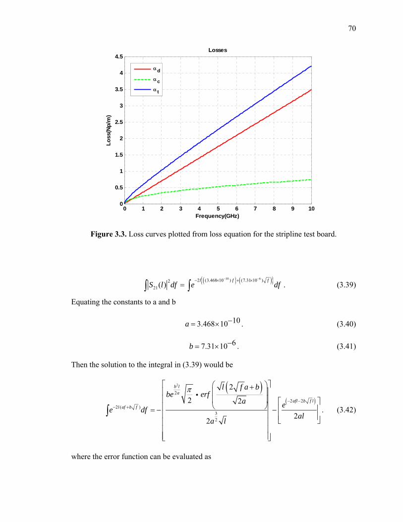
70
Figure 3.3. Loss curves plotted from loss equation for the stripline test board.
( ) ( ) 10 62 (3.468 10 ) (7.31 10 )221( )
l f fS l df e df
− −− × + ×=∫ ∫ . (3.39)
Equating the constants to a and b
103.468 10a −= × . (3.40)
67.31 10b −= × . (3.41)
Then the solution to the integral in (3.39) would be
( )( )
2
2
2 22 ( )
32
2
2 2
22
b la
afl b f ll af b f
l f a bbe erf
a ee dfala l
π− −
− +
⎡ ⎤⎛ ⎞+⎢ ⎥⎜ ⎟⎢ ⎥⎜ ⎟ ⎡ ⎤⎝ ⎠⎢ ⎥ ⎢ ⎥= − −⎢ ⎥ ⎢ ⎥⎣ ⎦⎢ ⎥⎢ ⎥⎢ ⎥⎣ ⎦
∫
i
. (3.42)
where the error function can be evaluated as
0 1 2 3 4 5 6 7 8 9 100
0.5
1
1.5
2
2.5
3
3.5
4
4.5Losses
Frequency(GHz)
Loss
(Np/
m)
αd
αcα t
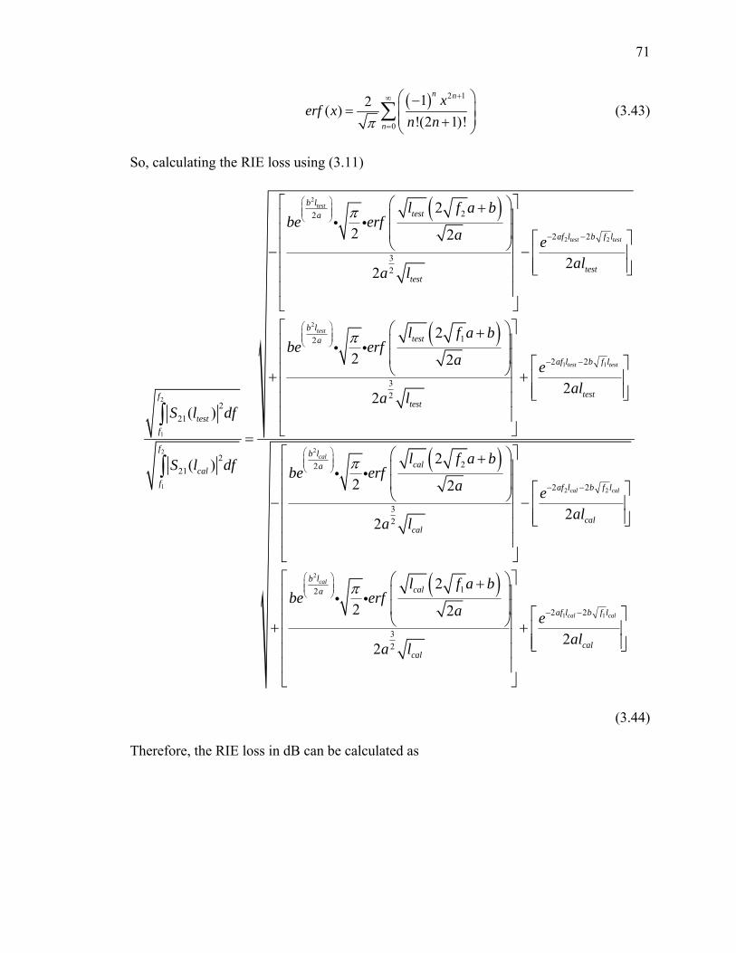
71
( ) 2 1
0
12( )!(2 1)!
n n
n
xerf x
n nπ
+∞
=
⎛ ⎞−= ⎜ ⎟
⎜ ⎟+⎝ ⎠∑ (3.43)
So, calculating the RIE loss using (3.11)
( )
( )
2
2 2
2
2
1
2
1
22
2 2
32
12
32
221
221
2
2 2
22
2
2 2
2( )
( )
test
test test
test
b ltesta
af l b f l
testtest
b ltesta
ft
testf
f
calf
l f a bbe erf
a eala l
l f a bbe erf
a
a lS l df
S l df
π
π
⎛ ⎞⎜ ⎟⎜ ⎟⎝ ⎠
− −
⎛ ⎞⎜ ⎟⎜ ⎟⎝ ⎠
⎡ ⎤⎛ ⎞+⎢ ⎥⎜ ⎟⎢ ⎥⎜ ⎟ ⎡ ⎤⎝ ⎠⎢ ⎥− − ⎢ ⎥⎢ ⎥ ⎢ ⎥⎣ ⎦⎢ ⎥⎢ ⎥⎣ ⎦
⎛ ⎞+⎜ ⎟⎜ ⎟⎝ ⎠+
=∫
∫
i i
i i
( )
( )
1 1
2
2 2
2
2 2
22
2 2
32
12
2
2
2 2
22
2
2 2
test test
cal
cal cal
cal
af l b f l
testest
b lcala
af l b f l
calcal
b lcala
eal
l f a bbe erf
a eala l
l f a bbe erf
a
π
π
− −
⎛ ⎞⎜ ⎟⎜ ⎟⎝ ⎠
− −
⎛ ⎞⎜ ⎟⎜ ⎟⎝ ⎠
⎡ ⎤⎢ ⎥⎢ ⎥ ⎡ ⎤⎢ ⎥ + ⎢ ⎥⎢ ⎥ ⎢ ⎥⎣ ⎦⎢ ⎥⎢ ⎥⎣ ⎦
⎡ ⎤⎛ ⎞+⎢ ⎥⎜ ⎟⎢ ⎥⎜ ⎟ ⎡ ⎤⎝ ⎠⎢ ⎥− − ⎢ ⎥⎢ ⎥ ⎢ ⎥⎣ ⎦⎢ ⎥⎢ ⎥⎣ ⎦
⎛ +
⎝+
i i
i i1 12 2
32 22
cal calaf l b f l
calcal
eala l
− −
⎡ ⎤⎞⎢ ⎥⎜ ⎟⎢ ⎥⎜ ⎟ ⎡ ⎤⎠⎢ ⎥ + ⎢ ⎥⎢ ⎥ ⎢ ⎥⎣ ⎦⎢ ⎥⎢ ⎥⎣ ⎦
(3.44)
Therefore, the RIE loss in dB can be calculated as
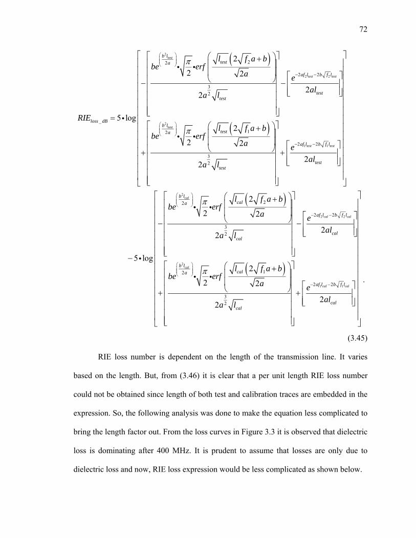
72
( )
( )
2
2 2
2
22
2 2
32
_
12
32
2
2 2
22
5 log2
2 2
2
test
test test
test
b ltesta
af l b f l
testtest
loss dBb l
testa
test
l f a bbe erf
a eala l
RIEl f a b
be erfa
a l
π
π
⎛ ⎞⎜ ⎟⎜ ⎟⎝ ⎠
− −
⎛ ⎞⎜ ⎟⎜ ⎟⎝ ⎠
⎡ ⎤⎛ ⎞+⎢ ⎥⎜ ⎟⎢ ⎥⎜ ⎟ ⎡ ⎤⎝ ⎠⎢ ⎥− − ⎢ ⎥⎢ ⎥ ⎢ ⎥⎣ ⎦⎢ ⎥⎢ ⎥⎢ ⎥⎣ ⎦=⎡ ⎤⎛ ⎞+⎢ ⎥⎜ ⎟⎢ ⎥⎜ ⎟
⎝ ⎠⎢ ⎥+⎢ ⎥⎢⎢⎢⎣ ⎦
i i
i
i i
( )
1 1
2
2 2
2
2 2
22
2 2
32
2
2
2
2 2
22
5 log
test test
cal
cal cal
cal
af l b f l
test
b lcala
af l b f l
calcal
b la
eal
l f a bbe erf
a eala l
be
π
− −
⎛ ⎞⎜ ⎟⎜ ⎟⎝ ⎠
− −
⎛⎜⎝
⎡ ⎤⎢ ⎥⎢ ⎥⎢ ⎥⎢ ⎥⎢ ⎥⎢ ⎥⎢ ⎥⎢ ⎥⎢ ⎥⎢ ⎥⎢ ⎥⎡ ⎤⎢ ⎥+ ⎢ ⎥⎢ ⎥⎢ ⎥⎣ ⎦⎥⎢ ⎥
⎥⎢ ⎥⎥⎣ ⎦
⎡ ⎤⎛ ⎞+⎢ ⎥⎜ ⎟⎢ ⎥⎜ ⎟ ⎡ ⎤⎝ ⎠⎢ ⎥− − ⎢ ⎥⎢ ⎥ ⎢ ⎥⎣ ⎦⎢ ⎥⎢ ⎥⎢ ⎥⎣ ⎦−
+
i i
i( )
1 1
1
2 2
32
2
2 2
22
cal cal
cal
af l b f l
calcal
l f a berf
a eala l
π⎞⎟⎜ ⎟⎠
− −
⎡ ⎤⎢ ⎥⎢ ⎥⎢ ⎥⎢ ⎥⎢ ⎥⎢ ⎥⎢ ⎥⎢ ⎥
⎡ ⎤⎛ ⎞⎢ + ⎥⎢ ⎥⎜ ⎟⎢ ⎥⎢ ⎥⎜ ⎟⎢ ⎥⎡ ⎤⎝ ⎠⎢ ⎥⎢ ⎥+ ⎢ ⎥⎢ ⎥⎢ ⎥⎢ ⎥⎣ ⎦⎢ ⎥⎢ ⎥⎢ ⎥⎢ ⎥⎢ ⎥⎣ ⎦⎣ ⎦
i i .
(3.45)
RIE loss number is dependent on the length of the transmission line. It varies
based on the length. But, from (3.46) it is clear that a per unit length RIE loss number
could not be obtained since length of both test and calibration traces are embedded in the
expression. So, the following analysis was done to make the equation less complicated to
bring the length factor out. From the loss curves in Figure 3.3 it is observed that dielectric
loss is dominating after 400 MHz. It is prudent to assume that losses are only due to
dielectric loss and now, RIE loss expression would be less complicated as shown below.

73
If αd dominates,
2 2
1 1
2 221( ) d
f fl
f f
S l df e dfα−=∫ ∫ . (3.46)
( )2 2 10
1 1
2 3.468 10221( )
f fl f
f f
S l df e df−− ×
=∫ ∫ . (3.47)
Evaluating the integral in (3.47)
( )
( )( )
( )
10 102 12
1
6.936 10 6.936 102
21 10 10( )
6.936 10 6.936 10
l f l ff
f
e eS l dfl l
− −− × − ×
− −
⎛ ⎞ ⎛ ⎞⎜ ⎟ ⎜ ⎟= −⎜ ⎟ ⎜ ⎟− × − ×⎝ ⎠ ⎝ ⎠
∫ . (3.48)
Therefore, square root of (3.48) gives
( )
( )( )
( )
10 102 12
1
6.936 10 6.936 102
21 10 10( )
6.936 10 6.936 10
l f l ff
f
e eS l dfl l
− −− × − ×
− −
⎛ ⎞ ⎛ ⎞⎜ ⎟ ⎜ ⎟= −⎜ ⎟ ⎜ ⎟− × − ×⎝ ⎠ ⎝ ⎠
∫ . (3.49)
To calculate RIE loss it is required to consider a test trace (ltest) and a calibration trace
(lcal). Then the expression for RIE loss would be
( )
( )( )
( )( )
( )( )
10 102 1
2
1
10 102 2 1
1
6.936 10 6.936 102
10 1021
6.936 10 6.936 10221
10
( ) 6.936 10 6.936 10
( )6.936 10 6.936
test test
cal cal
l f l ff
testtest testf
f l f l f
calf cal cal
e eS l df l l
e eS l dfl l
− −
− −
− × − ×
− −
− × − ×
−
⎛ ⎞ ⎛ ⎞⎜ ⎟ ⎜ ⎟−⎜ ⎟ ⎜ ⎟− × − ×⎝ ⎠ ⎝ ⎠=⎛ ⎞⎜ ⎟ −⎜ ⎟− × −⎝ ⎠
∫
∫ ( )1010−
⎛ ⎞⎜ ⎟⎜ ⎟×⎝ ⎠
. (3.50)
Further simplification of (3.50) and converting it to dB provides leads to
10 106.936 10 6.936 102 1
10 106.936 10 6.936 102 1_ 10 log 10 logf l f ltest test
f l f lcal cal
calloss dB
test
l e eRIEl e e
− −− × − ×
− −− × − ×
⎛ ⎞⎛ ⎞ −⎜ ⎟= +⎜ ⎟⎜ ⎟ ⎜ ⎟−⎝ ⎠ ⎝ ⎠
i i . (3.51)
10 106.936 10 6.936 102 1
10 106.936 10 6.936 102 1_ 5 log 5 logf l f ltest test
f l f lcal cal
calloss dB
test
l e eRIEl e e
− −− × − ×
− −− × − ×
⎛ ⎞⎛ ⎞ −⎜ ⎟= +⎜ ⎟ ⎜ ⎟⎝ ⎠ −⎝ ⎠i i . (3.52)
74
From (3.53) it is clear that, even now the length is embedded in the equation and it is
impossible to extract a per unit length RIE loss parameter.
3.4. MEASUREMENTS AND RESULTS
From the previous section, three sets of comparisons were detailed to verify the
RIE loss number: frequency domain method, time domain method and the analytical
expression. Frequency domain measurements were made on the stripline test board with
HP8270ES Network Analyzer and time domain measurements were done with Agilent
Infiniium DCA 86100B. Analytical calculations were done in MATLAB.
3.4.1. Frequency Domain Measurements. Calibration is important for this
study to quantify the loss of the trace and it is required to avoid effects of via, transitions
etc. TRL calibration was used which was explained in Section 2.1.3. Three different
frequency ranges were used and calibrated separately. Once calibration was done,
measurements were taken on the traces shown in Table 3.2. The test board was the same
as shown in Figure 2.5. And the test setup used was the same as the one shown in Figure
2.8. S-parameters of all the traces shown in Table 3.2 were measured and plotted for
further analysis. Figure 3.4 shows the measurement results.
Table 3.2. Length of traces used in the stripline test board.
Traces Length (inches)SSL3 (Calibration) 0.125 SSL2 (Calibration) 0.579 SSL1 (Test) 2.679 ST1-2 (Test) 7.976
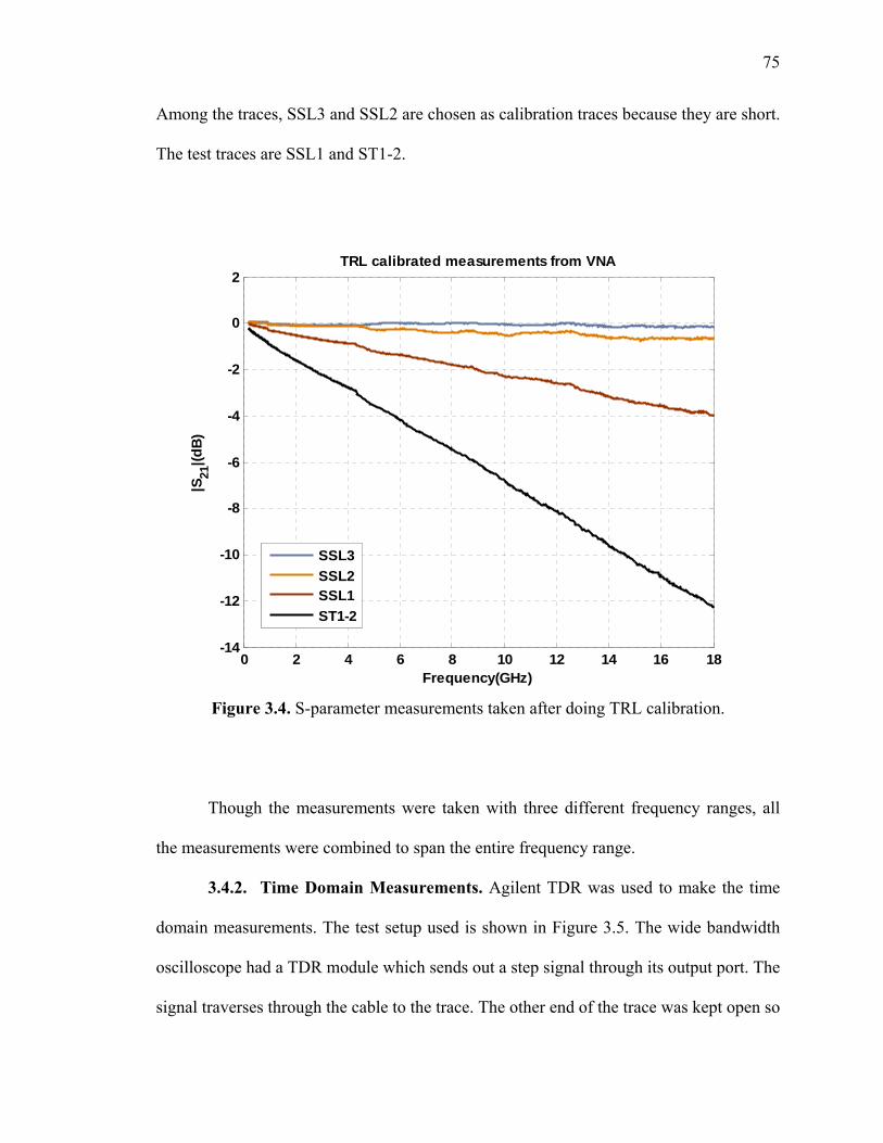
75
Among the traces, SSL3 and SSL2 are chosen as calibration traces because they are short.
The test traces are SSL1 and ST1-2.
0 2 4 6 8 10 12 14 16 18-14
-12
-10
-8
-6
-4
-2
0
2TRL calibrated measurements from VNA
Frequency(GHz)
|S21
|(dB)
SSL3SSL2SSL1ST1-2
Figure 3.4. S-parameter measurements taken after doing TRL calibration.
Though the measurements were taken with three different frequency ranges, all
the measurements were combined to span the entire frequency range.
3.4.2. Time Domain Measurements. Agilent TDR was used to make the time
domain measurements. The test setup used is shown in Figure 3.5. The wide bandwidth
oscilloscope had a TDR module which sends out a step signal through its output port. The
signal traverses through the cable to the trace. The other end of the trace was kept open so
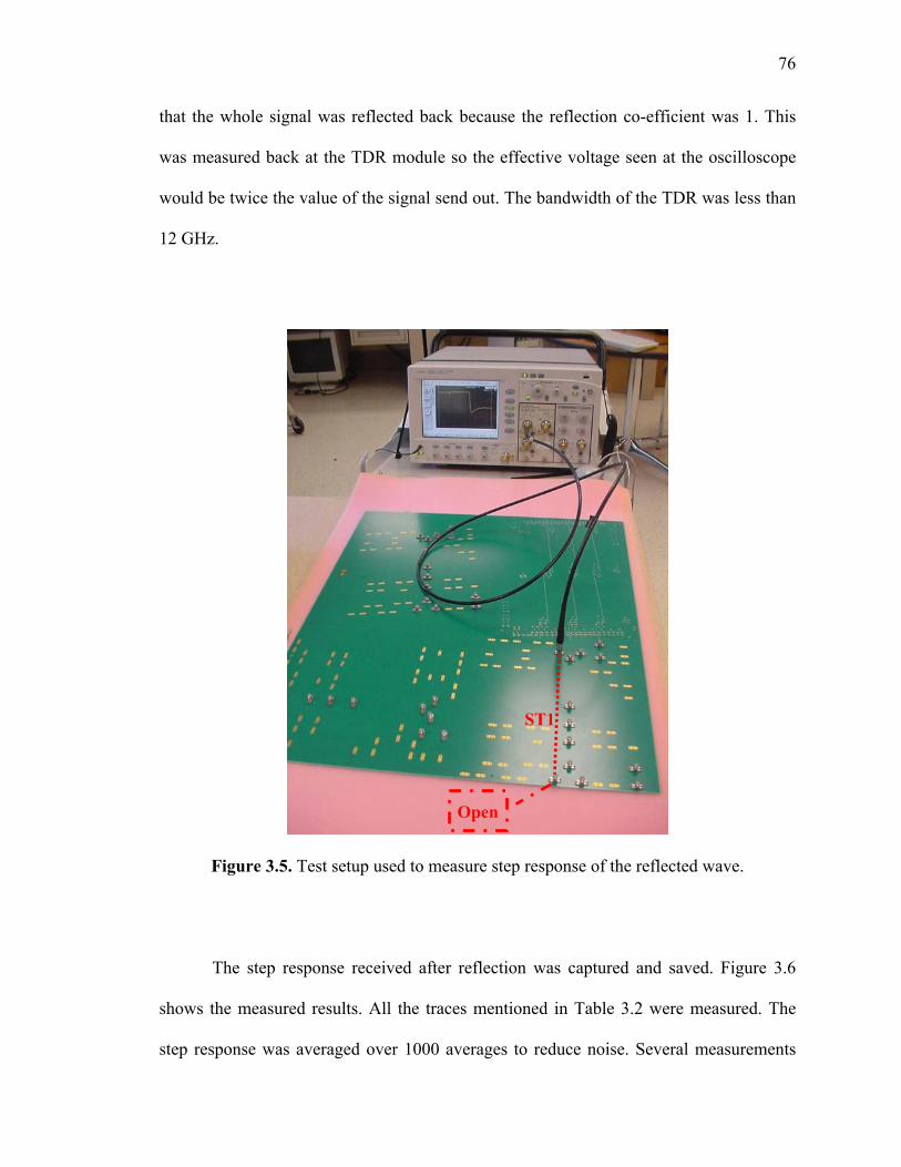
76
that the whole signal was reflected back because the reflection co-efficient was 1. This
was measured back at the TDR module so the effective voltage seen at the oscilloscope
would be twice the value of the signal send out. The bandwidth of the TDR was less than
12 GHz.
Figure 3.5. Test setup used to measure step response of the reflected wave. The step response received after reflection was captured and saved. Figure 3.6
shows the measured results. All the traces mentioned in Table 3.2 were measured. The
step response was averaged over 1000 averages to reduce noise. Several measurements
Open
ST1
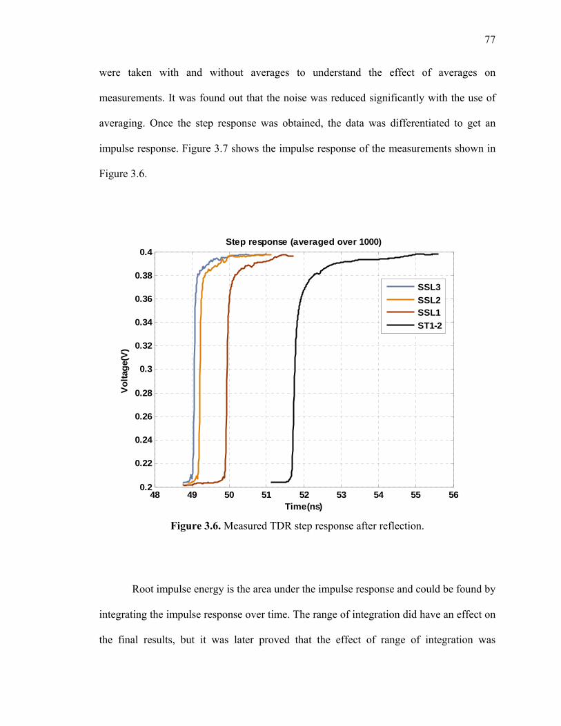
77
were taken with and without averages to understand the effect of averages on
measurements. It was found out that the noise was reduced significantly with the use of
averaging. Once the step response was obtained, the data was differentiated to get an
impulse response. Figure 3.7 shows the impulse response of the measurements shown in
Figure 3.6.
48 49 50 51 52 53 54 55 560.2
0.22
0.24
0.26
0.28
0.3
0.32
0.34
0.36
0.38
0.4Step response (averaged over 1000)
Time(ns)
Vol
tage
(V)
SSL3SSL2SSL1ST1-2
Figure 3.6. Measured TDR step response after reflection.
Root impulse energy is the area under the impulse response and could be found by
integrating the impulse response over time. The range of integration did have an effect on
the final results, but it was later proved that the effect of range of integration was
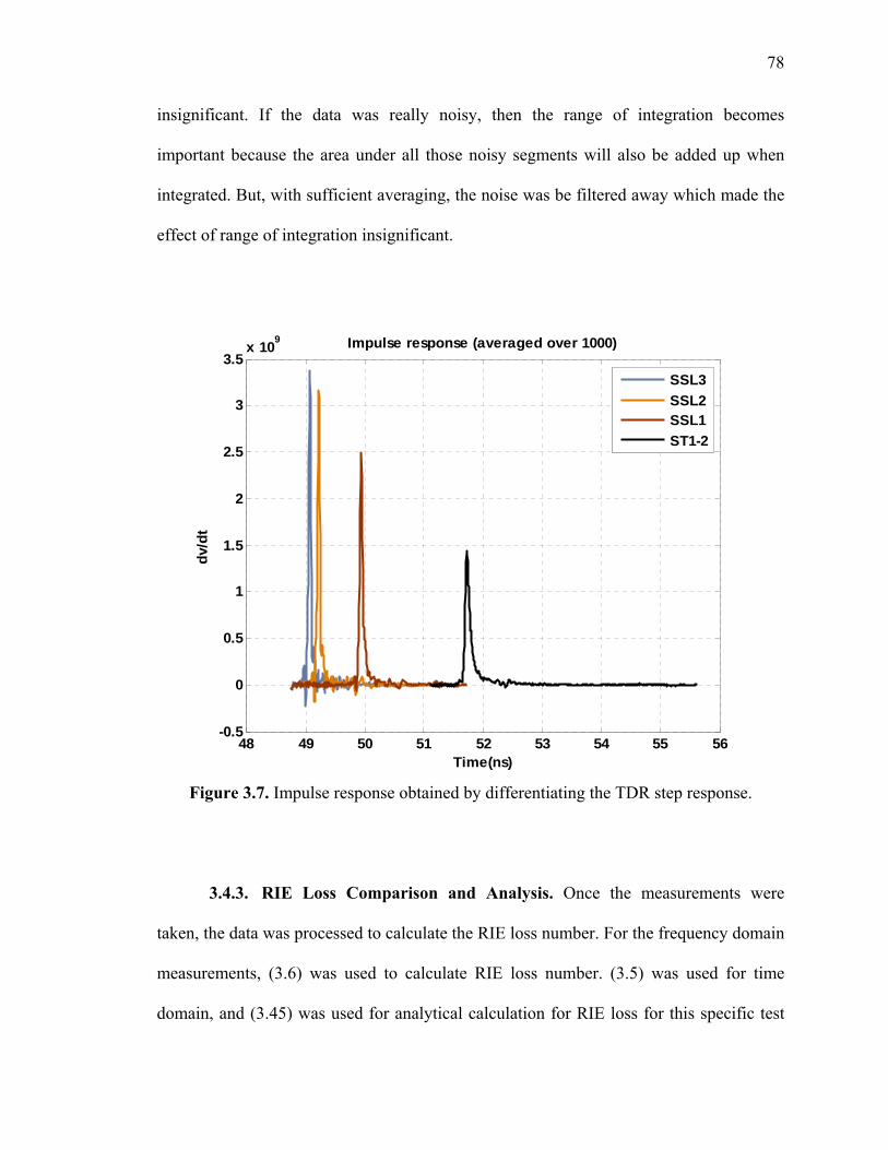
78
insignificant. If the data was really noisy, then the range of integration becomes
important because the area under all those noisy segments will also be added up when
integrated. But, with sufficient averaging, the noise was be filtered away which made the
effect of range of integration insignificant.
48 49 50 51 52 53 54 55 56-0.5
0
0.5
1
1.5
2
2.5
3
3.5x 10⁹ Impulse response (averaged over 1000)
Time(ns)
dv/d
t
SSL3SSL2SSL1ST1-2
Figure 3.7. Impulse response obtained by differentiating the TDR step response.
3.4.3. RIE Loss Comparison and Analysis. Once the measurements were
taken, the data was processed to calculate the RIE loss number. For the frequency domain
measurements, (3.6) was used to calculate RIE loss number. (3.5) was used for time
domain, and (3.45) was used for analytical calculation for RIE loss for this specific test
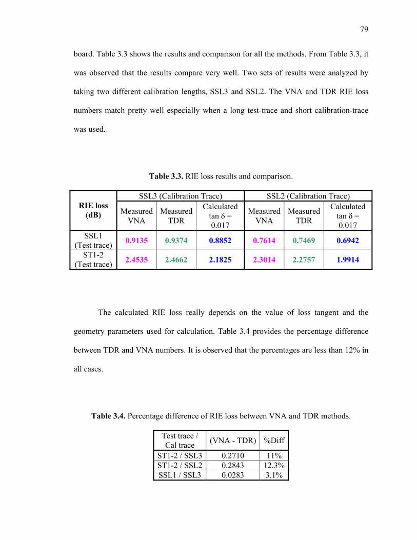
79
board. Table 3.3 shows the results and comparison for all the methods. From Table 3.3, it
was observed that the results compare very well. Two sets of results were analyzed by
taking two different calibration lengths, SSL3 and SSL2. The VNA and TDR RIE loss
numbers match pretty well especially when a long test-trace and short calibration-trace
was used.
Table 3.3. RIE loss results and comparison.
SSL3 (Calibration Trace) SSL2 (Calibration Trace) RIE loss
(dB) Measured VNA
MeasuredTDR
Calculated tan δ = 0.017
MeasuredVNA
Measured TDR
Calculated tan δ = 0.017
SSL1 (Test trace) 0.9135 0.9374 0.8852 0.7614 0.7469 0.6942
ST1-2 (Test trace) 2.4535 2.4662 2.1825 2.3014 2.2757 1.9914
The calculated RIE loss really depends on the value of loss tangent and the
geometry parameters used for calculation. Table 3.4 provides the percentage difference
between TDR and VNA numbers. It is observed that the percentages are less than 12% in
all cases.
Table 3.4. Percentage difference of RIE loss between VNA and TDR methods.
Test trace / Cal trace (VNA - TDR) %Diff
ST1-2 / SSL3 0.2710 11% ST1-2 / SSL2 0.2843 12.3%SSL1 / SSL3 0.0283 3.1%
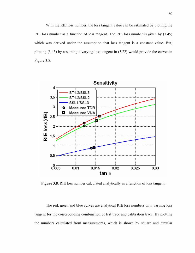
80
With the RIE loss number, the loss tangent value can be estimated by plotting the
RIE loss number as a function of loss tangent. The RIE loss number is given by (3.45)
which was derived under the assumption that loss tangent is a constant value. But,
plotting (3.45) by assuming a varying loss tangent in (3.22) would provide the curves in
Figure 3.8.
Figure 3.8. RIE loss number calculated analytically as a function of loss tangent. The red, green and blue curves are analytical RIE loss numbers with varying loss
tangent for the corresponding combination of test trace and calibration trace. By plotting
the numbers calculated from measurements, which is shown by square and circular
81
points, approximate value of loss tangent can be obtained from measurement results.
Table 3.5 shows the projected value of loss tangent for each measurement.
Table 3.5. Projected value of loss tangent from RIE loss curves.
Test trace / Cal trace
tan δ (VNA)
tan δ (TDR)
ST1-2 / SSL3 0.0159 0.0121ST1-2 / SSL2 0.0153 0.0121SSL1 / SSL3 0.0146 0.0139
From Table 3.1, VNA measurements, which was our standard, is giving loss
tangent values close to what was extracted. The extracted value for this material was
0.017 and VNA RIE loss number corresponds to almost 0.016. But, TDR RIE loss
number, which were not very accurate correspond to a value close to 0.012. More
research is needed to make sure that TDR measurements are much more accurate and
corresponding RIE loss values, because the TDR measurements are dependent on the
bandwidth of the equipment. Once it is made sure that VNA and TDR are providing
comparable measurement results, this method could prove to be a standard in extracting
the loss parameters with the help of time domain equipments like TDR. Thus, RIE loss
number could be used as a standard to estimate losses in a printed circuit board (PCB).
82
4. ANALYSIS, MODELING AND VALIDATION Cost-effective, efficient, and fast signal link path designs require careful modeling
strategies. Several tools are available in the market to do time and frequency domain
simulations for signal integrity analysis. Static time domain solvers provide us quick
results while full wave simulations take longer. But, full wave simulations provide us
with more accurate results. But, modeling is not an easy task. The user not only has to
understand the problem very well but also needs to understand how to use the tool
effectively. Simple problems also need careful modeling to assure that the results
obtained are correct. Once modeling is done, it is very important to make sure that the
results are meaningful and corresponds to what was expected. Experience with signal
integrity analysis and tools, could solve this problem easily. But, for a beginner, he could
try to validate the results by developing analytical solutions. As the problem becomes
complex, developing analytical solutions become tedious. Then, the best way to validate
the results would be to use several different tools available in the market. Comparisons
will lead to a better understanding of modeling and more accurate solutions. This Section
deals with two simple signal integrity modeling problems.
First, the problem considers a dielectric slab placed in an air-medium. A plane
wave passes through this dielectric slab. The time delays for the plane wave traveling
through air and through a dielectric medium will be different because of the material
properties. Those time delays and reflections, at air and dielectric boundaries are
analyzed using two different tools.
Design of power distribution networks (PDNs) on a printed circuit board (PCB) is
very important for proper charge delivery to the devices on the board. Lowering the
83
impedance is the key for efficient PDN design. Second problem deals with the modeling
of a large PCB with a source at the center. Effects of using decoupling capacitors on
transfer impedance are analyzed. Location and value of capacitors were changed to see
how it affects the transfer impedance. The results are validated using three tools.
4.1. PROPAGATION DELAY THROUGH A DIELECTRIC SLAB
The problem considers the propagation of a plane wave through a dielectric slab.
The dielectric constant of the slab is varied to see the effects of it on the propagation
delay. As the plane wave passes through the dielectric medium, the time it takes to pass
depends on the dielectric constant of the slab. If dielectric constant is increased, the plane
wave takes more time to pass through the medium since time delay is directly
proportional to the square root of dielectric constant. The problem here compares a thin
slab with dielectric constants 2.5, 5 and 10.
4.1.1. Geometry Description. The problem as shown in Figure 4.1, considers a
5 cm thick dielectric slab with width and length large enough to be considered as infinite.
This is to avoid the boundary effects that could possibly be a part of the end results. A
Gaussian plane wave source is considered here which is approaching from x = minus
infinity direction. So, the plane wave is propagating along the x-axis.
4.1.2. Time Delay Calculation. The velocity of propagation (vp) of a wave
traveling through the slab with dielectric constant (εr) is given by
Velocity of propagation, pr
cvε
= . (4.1)
Time delay, dp
dtv
= . (4.2)
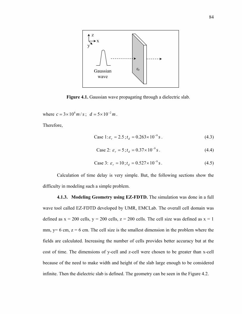
84
Figure 4.1. Gaussian wave propagating through a dielectric slab.
where smc /103 8×= ; md 2105 −×= .
Therefore,
Case 1: 2.5rε = ; std910263.0 −×= . (4.3)
Case 2: 5=rε ; std91037.0 −×= . (4.4)
Case 3: 10=rε ; std910527.0 −×= . (4.5)
Calculation of time delay is very simple. But, the following sections show the
difficulty in modeling such a simple problem.
4.1.3. Modeling Geometry using EZ-FDTD. The simulation was done in a full
wave tool called EZ-FDTD developed by UMR, EMCLab. The overall cell domain was
defined as x = 200 cells, y = 200 cells, z = 200 cells. The cell size was defined as x = 1
mm, y= 6 cm, z = 6 cm. The cell size is the smallest dimension in the problem where the
fields are calculated. Increasing the number of cells provides better accuracy but at the
cost of time. The dimensions of y-cell and z-cell were chosen to be greater than x-cell
because of the need to make width and height of the slab large enough to be considered
infinite. Then the dielectric slab is defined. The geometry can be seen in the Figure 4.2.
εr Gaussian wave
x z
y
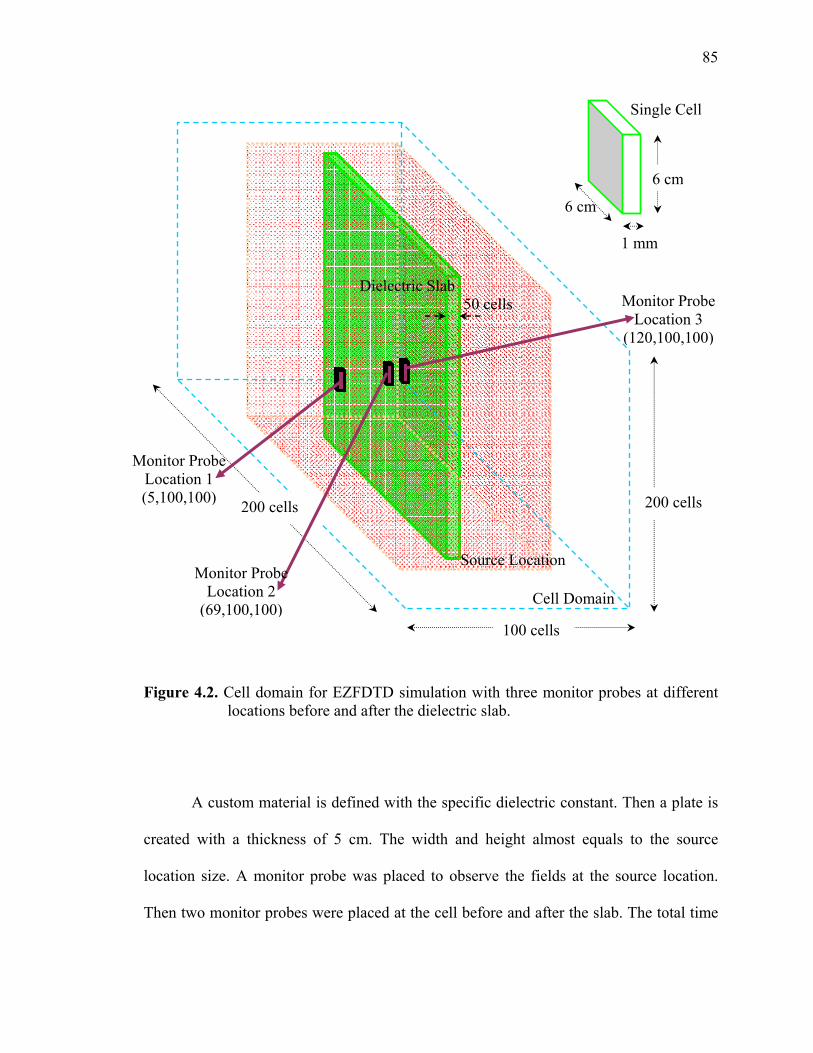
85
Figure 4.2. Cell domain for EZFDTD simulation with three monitor probes at different locations before and after the dielectric slab.
A custom material is defined with the specific dielectric constant. Then a plate is
created with a thickness of 5 cm. The width and height almost equals to the source
location size. A monitor probe was placed to observe the fields at the source location.
Then two monitor probes were placed at the cell before and after the slab. The total time
100 cells
200 cells
50 cells
6 cm
6 cm
1 mm
Single Cell
Cell Domain
Source Location
Dielectric Slab
Monitor Probe Location 2
(69,100,100)
Monitor Probe Location 3
(120,100,100)
200 cells
Monitor Probe Location 1 (5,100,100)
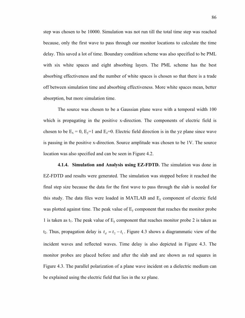
86
step was chosen to be 10000. Simulation was not run till the total time step was reached
because, only the first wave to pass through our monitor locations to calculate the time
delay. This saved a lot of time. Boundary condition scheme was also specified to be PML
with six white spaces and eight absorbing layers. The PML scheme has the best
absorbing effectiveness and the number of white spaces is chosen so that there is a trade
off between simulation time and absorbing effectiveness. More white spaces mean, better
absorption, but more simulation time.
The source was chosen to be a Gaussian plane wave with a temporal width 100
which is propagating in the positive x-direction. The components of electric field is
chosen to be Ex = 0, Ey=1 and Ez=0. Electric field direction is in the yz plane since wave
is passing in the positive x-direction. Source amplitude was chosen to be 1V. The source
location was also specified and can be seen in Figure 4.2.
4.1.4. Simulation and Analysis using EZ-FDTD. The simulation was done in
EZ-FDTD and results were generated. The simulation was stopped before it reached the
final step size because the data for the first wave to pass through the slab is needed for
this study. The data files were loaded in MATLAB and Ey component of electric field
was plotted against time. The peak value of Ey component that reaches the monitor probe
1 is taken as t1. The peak value of Ey component that reaches monitor probe 2 is taken as
t2. Thus, propagation delay is 12 tttd −= . Figure 4.3 shows a diagrammatic view of the
incident waves and reflected waves. Time delay is also depicted in Figure 4.3. The
monitor probes are placed before and after the slab and are shown as red squares in
Figure 4.3. The parallel polarization of a plane wave incident on a dielectric medium can
be explained using the electric field that lies in the xz plane.
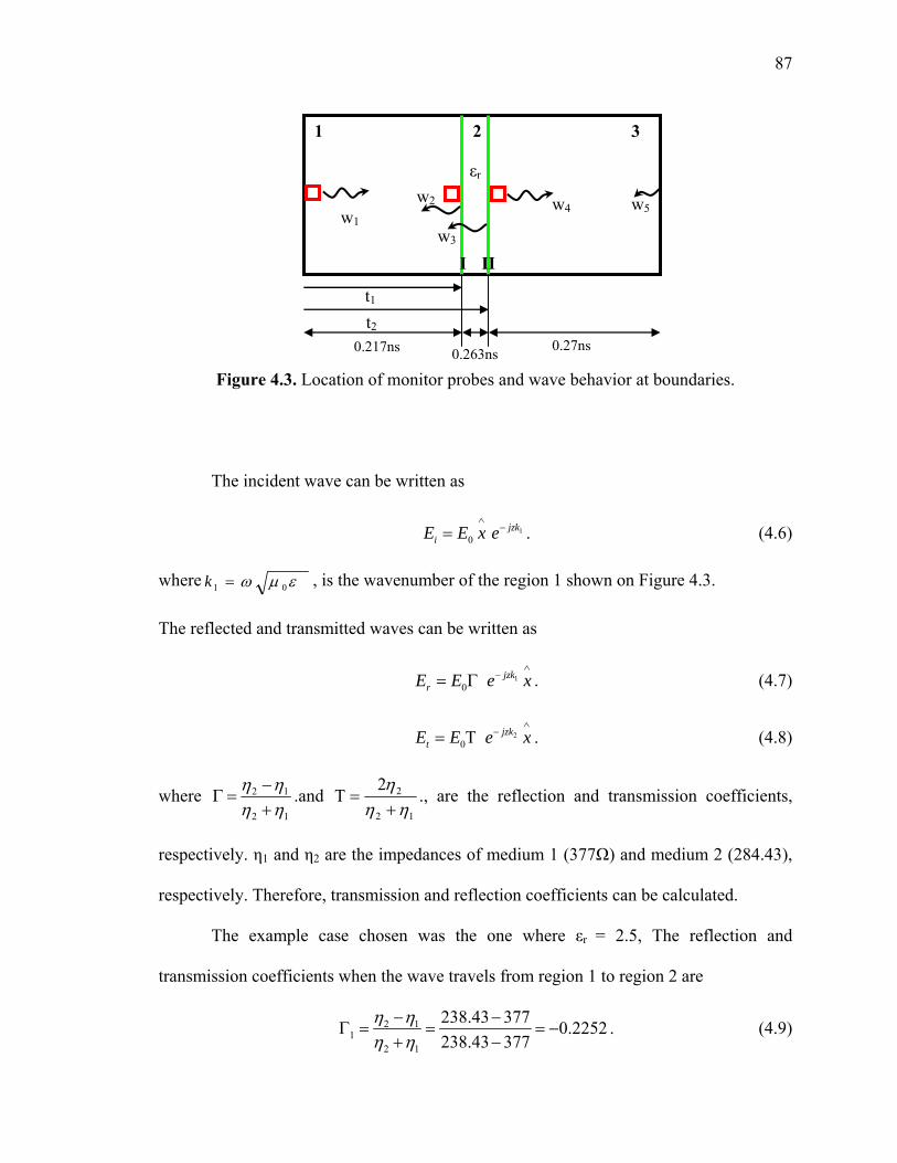
87
Figure 4.3. Location of monitor probes and wave behavior at boundaries.
The incident wave can be written as
10
jzkiE E x e
∧−= . (4.6)
where εμω 01 =k , is the wavenumber of the region 1 shown on Figure 4.3.
The reflected and transmitted waves can be written as
10
jzkrE E e x
∧−= Γ . (4.7)
20
jzktE E e x
∧−= Τ . (4.8)
where 12
12
ηηηη
+−
=Γ .and 12
22ηη
η+
=Τ ., are the reflection and transmission coefficients,
respectively. η1 and η2 are the impedances of medium 1 (377Ω) and medium 2 (284.43),
respectively. Therefore, transmission and reflection coefficients can be calculated.
The example case chosen was the one where εr = 2.5, The reflection and
transmission coefficients when the wave travels from region 1 to region 2 are
2 11
2 1
238.43 377 0.2252238.43 377
η ηη η
− −Γ = = = −
+ −. (4.9)
t1 t2
εr
w1 w2
w3
w4 w5
0.217ns 0.263ns 0.27ns
1 2 3
I II

88
21
2 1
2 2*238.43 0.7748238.43 377
ηη η
Τ = = =+ +
. (4.10)
The reflection and transmission coefficients when the wave travels from region 2 to
region 3 are
2 12
2 1
377 238.43 0.2252377 238.43
η ηη η
− −Γ = = =
+ +. (4.11)
22
2 1
2 2*377 1.2252238.43 377
ηη η
Τ = = =+ +
. (4.12)
For monitor probe 1 (at the source), the magnitude of Ey when Eo = 1 V/m is the
wave reflected from surface 1 and is seen at probe 1
( )1 0 1 1 0.2252 0.2252 /yE E V m= ⋅Γ = − = − . (4.13)
Wave transmitted from surface 1, reflected from surface 2 and transmitted back from
surface 1 is calculated as
( )121 0 1 2 2 1* 0.7748*0.2252*1.2252 0.2138 /yE E V m= ⋅Τ ⋅Γ ⋅Τ = = . (4.14)
The wave observed at probe 1 are w1 and the reflected waves w2, w3. There will also be
reflections from w5, but they will be quite small. It takes, t = 0.93ns for the wave to reach
monitor probe 1. Then it passes through free space and reaches the monitor probe 2(just
before the dielectric slab) which is 0.065m away. The time of travel is
8
0.065 0.2173 10
t ns= =×
. (4.15)
w2 reaches monitor probe 1 in
(0.93 0.217 0.217) 1.364t ns ns= + + = . (4.16)
To calculate the reflected waves, the time the wave takes to pass through the dielectric
slab with εr = 2.5,

89
8
0.050 2.5 0.2633 10
t ns×= =
×. (4.17)
Therefore, w3 reaches monitor probe 1 in
(0.93 0.217 0.217 0.263 0.263) 1.89t ns ns= + + + + = . (4.18)
For monitor probe 2, the magnitude of Ey when Eo = 1V/m, is the wave reflected from
surface 1 and is seen at probe 2
( )2 0 1 1 0.2252 0.7748 /y yE E E V m= − = − = . (4.19)
Wave transmitted from surface 1, reflected from surface 2 and transmitted again from
surface 1 can be calculated as
( )21 2 2 2 0.7748*0.2252*1.2252 0.2138 /y yE E V m= ⋅Γ ⋅Τ = = . (4.20)
The total time it takes w1 to reach monitor probe 2 is
(0.93 0.217) 1.147t ns ns= + = . (4.21)
The w3 is coming back to monitor probe 2 in
(0.93 0.217 0.263 0.263) 1.673t ns ns= + + + = . (4.22)
For monitor probe 3, the magnitude of Ey when Eo = 1V/m, is the wave reflected
from surface 1 and is seen at probe 3 (wave transmitted from surface II)
3 0 1 2 1*0.7748*1.2252 0.9493 /yE E V m= ⋅Τ ⋅Τ = = . (4.23)
The wave reaches monitor probe 3 in
(0.93 0.217 0.263) 1.41t ns ns= + + = . (4.24)
The monitor probe 2 is showing much lesser amplitude for Ey as that of the source
because some of the field components reflected from the slab boundary is out of phase
with the incident wave and cancels off (as shown in (4.19)). There are reflections from
the end of the source location too, but the value is quite small. The time delay values and
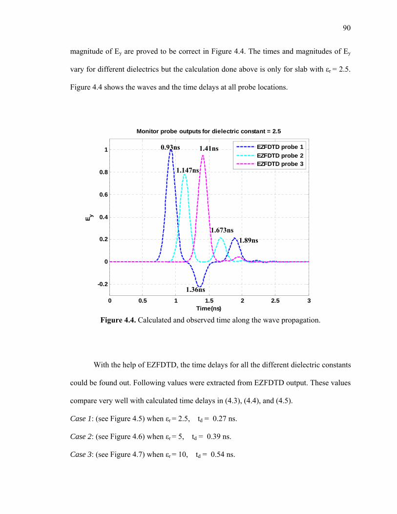
90
magnitude of Ey are proved to be correct in Figure 4.4. The times and magnitudes of Ey
vary for different dielectrics but the calculation done above is only for slab with εr = 2.5.
Figure 4.4 shows the waves and the time delays at all probe locations.
Figure 4.4. Calculated and observed time along the wave propagation.
With the help of EZFDTD, the time delays for all the different dielectric constants
could be found out. Following values were extracted from EZFDTD output. These values
compare very well with calculated time delays in (4.3), (4.4), and (4.5).
Case 1: (see Figure 4.5) when εr = 2.5, td = 0.27 ns.
Case 2: (see Figure 4.6) when εr = 5, td = 0.39 ns.
Case 3: (see Figure 4.7) when εr = 10, td = 0.54 ns.
0 0.5 1 1.5 2 2.5 3
-0.2
0
0.2
0.4
0.6
0.8
1
Monitor probe outputs for dielectric constant = 2.5
Time(ns)
E y
EZFDTD probe 1EZFDTD probe 2EZFDTD probe 3
0.93ns
1.36ns
1.89ns
1.41ns
1.147ns
1.673ns
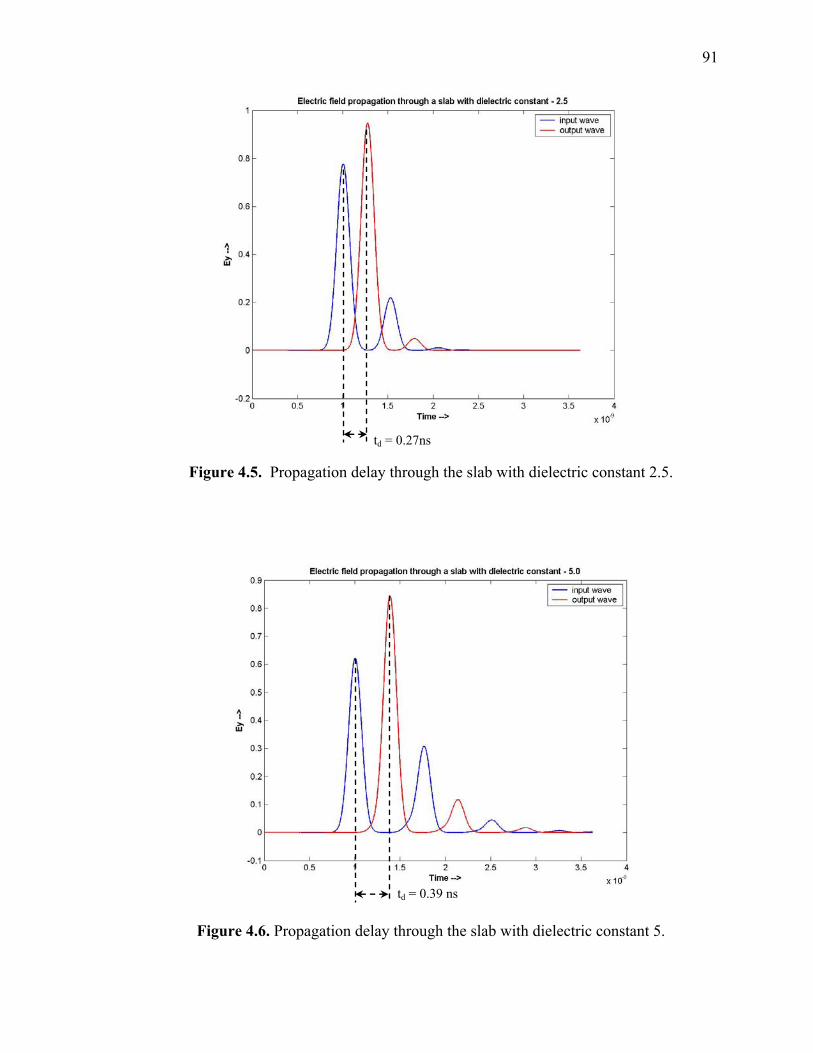
91
Figure 4.5. Propagation delay through the slab with dielectric constant 2.5.
Figure 4.6. Propagation delay through the slab with dielectric constant 5.
td = 0.27ns
td = 0.39 ns
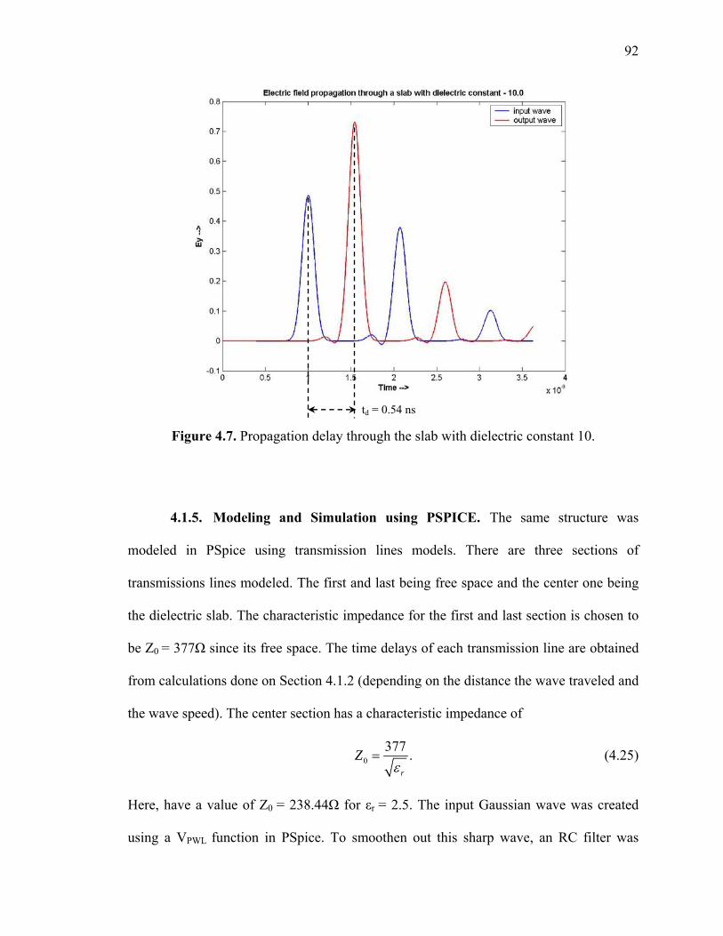
92
Figure 4.7. Propagation delay through the slab with dielectric constant 10.
4.1.5. Modeling and Simulation using PSPICE. The same structure was
modeled in PSpice using transmission lines models. There are three sections of
transmissions lines modeled. The first and last being free space and the center one being
the dielectric slab. The characteristic impedance for the first and last section is chosen to
be Z0 = 377Ω since its free space. The time delays of each transmission line are obtained
from calculations done on Section 4.1.2 (depending on the distance the wave traveled and
the wave speed). The center section has a characteristic impedance of
0377 .
r
Zε
= (4.25)
Here, have a value of Z0 = 238.44Ω for εr = 2.5. The input Gaussian wave was created
using a VPWL function in PSpice. To smoothen out this sharp wave, an RC filter was
td = 0.54 ns
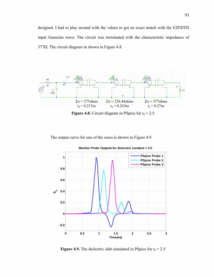
93
designed. I had to play around with the values to get an exact match with the EZFDTD
input Gaussian wave. The circuit was terminated with the characteristic impedance of
377Ω. The circuit diagram in shown in Figure 4.8.
Figure 4.8. Circuit diagram in PSpice for εr = 2.5.
The output curve for one of the cases is shown in Figure 4.9.
0 0.5 1 1.5 2 2.5 3
-0.2
0
0.2
0.4
0.6
0.8
1
Monitor Probe Outputs for dielectric constant = 2.5
Time(ns)
E y
PSpice Probe 1PSpice Probe 2PSpice Probe 3
Figure 4.9. The dielectric slab simulated in PSpice for εr = 2.5.
Zo = 377ohms td = 0.217ns
Zo = 238.44ohms td = 0.263ns
Zo = 377ohms td = 0.27ns
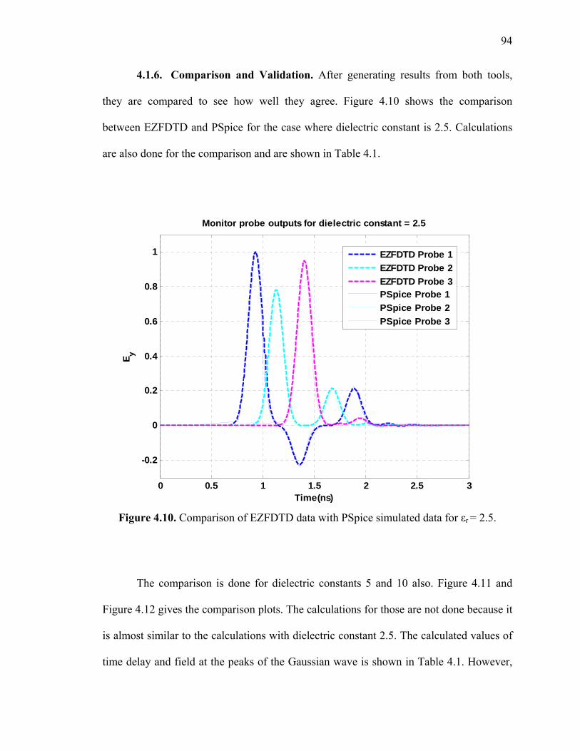
94
4.1.6. Comparison and Validation. After generating results from both tools,
they are compared to see how well they agree. Figure 4.10 shows the comparison
between EZFDTD and PSpice for the case where dielectric constant is 2.5. Calculations
are also done for the comparison and are shown in Table 4.1.
0 0.5 1 1.5 2 2.5 3
-0.2
0
0.2
0.4
0.6
0.8
1
Monitor probe outputs for dielectric constant = 2.5
Time(ns)
E y
EZFDTD Probe 1EZFDTD Probe 2EZFDTD Probe 3PSpice Probe 1PSpice Probe 2PSpice Probe 3
Figure 4.10. Comparison of EZFDTD data with PSpice simulated data for εr = 2.5.
The comparison is done for dielectric constants 5 and 10 also. Figure 4.11 and
Figure 4.12 gives the comparison plots. The calculations for those are not done because it
is almost similar to the calculations with dielectric constant 2.5. The calculated values of
time delay and field at the peaks of the Gaussian wave is shown in Table 4.1. However,
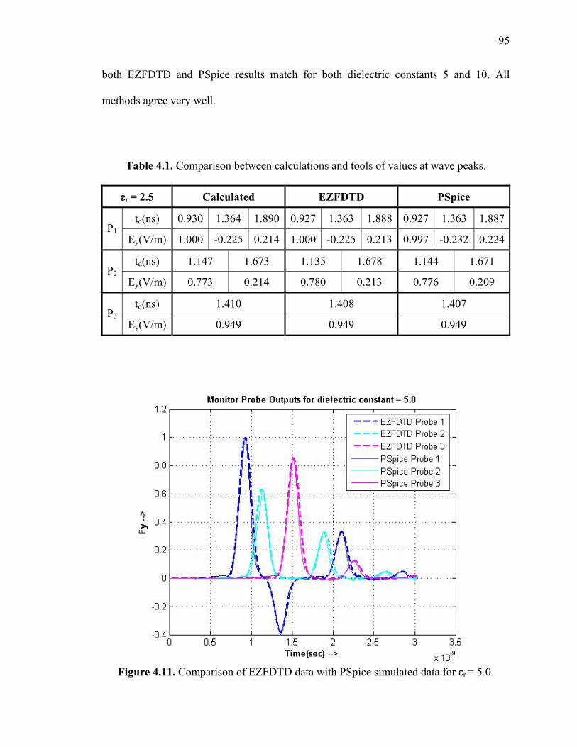
95
both EZFDTD and PSpice results match for both dielectric constants 5 and 10. All
methods agree very well.
Table 4.1. Comparison between calculations and tools of values at wave peaks.
εr = 2.5 Calculated EZFDTD PSpice
td(ns) 0.930 1.364 1.890 0.927 1.363 1.888 0.927 1.363 1.887P1
Ey(V/m) 1.000 -0.225 0.214 1.000 -0.225 0.213 0.997 -0.232 0.224
td(ns) 1.147 1.673 1.135 1.678 1.144 1.671 P2
Ey(V/m) 0.773 0.214 0.780 0.213 0.776 0.209
td(ns) 1.410 1.408 1.407 P3
Ey(V/m) 0.949 0.949 0.949
Figure 4.11. Comparison of EZFDTD data with PSpice simulated data for εr = 5.0.
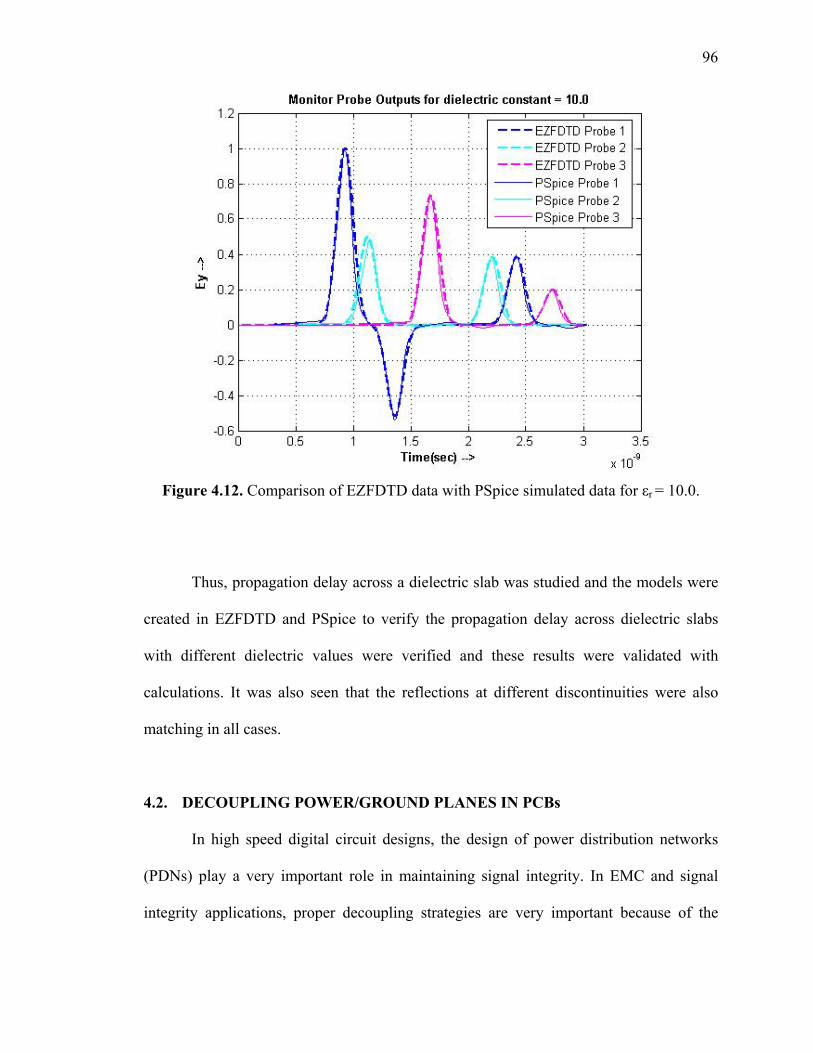
96
Figure 4.12. Comparison of EZFDTD data with PSpice simulated data for εr = 10.0.
Thus, propagation delay across a dielectric slab was studied and the models were
created in EZFDTD and PSpice to verify the propagation delay across dielectric slabs
with different dielectric values were verified and these results were validated with
calculations. It was also seen that the reflections at different discontinuities were also
matching in all cases.
4.2. DECOUPLING POWER/GROUND PLANES IN PCBs
In high speed digital circuit designs, the design of power distribution networks
(PDNs) play a very important role in maintaining signal integrity. In EMC and signal
integrity applications, proper decoupling strategies are very important because of the

97
requirement of sufficient current for a digital device on the printed circuit board (PCB)
for switching the transistors [14-17]. The problem considered here is a realistic-sized
printed circuit board with a power and a ground plane separated by FR4. Different
decoupling strategies are applied to see its effect on impedance at different locations on
the printed circuit board (PCB).
4.2.1. Geometry Description. The problem considers a printed circuit board,
with capacitors distributed across the entire board. The specifications are given below
and a diagram is provided in Figure 4.13. This problem includes a wide range of
frequencies, resonance effects, and the effects of lumped circuit elements.
General Board Description: 4-layer board with 2 solid planes in inner layers, solid planes
are separated by 40 mils dielectric FR4 (relative dielectric constant = 4.5).
PCB size: 10” x 12” inches.
Capacitors: 95 capacitors evenly spaced 1” apart, includes 30 mohms series resistance
and 2 nH series inductance.
Source: Located in center of board, 1-volt sine wave, frequency scanned from 10-1000
MHz.
Figure-of-merit: Impedance at output #1, #2, and #3
Following cases are considered for decoupling analysis:
1. Board with no capacitors.
2. Board with four capacitors only around source.
3. Board with fully loaded 95 capacitors.
4. Use capacitor values of 0.01 μF, 0.1 μF and 100 pF.
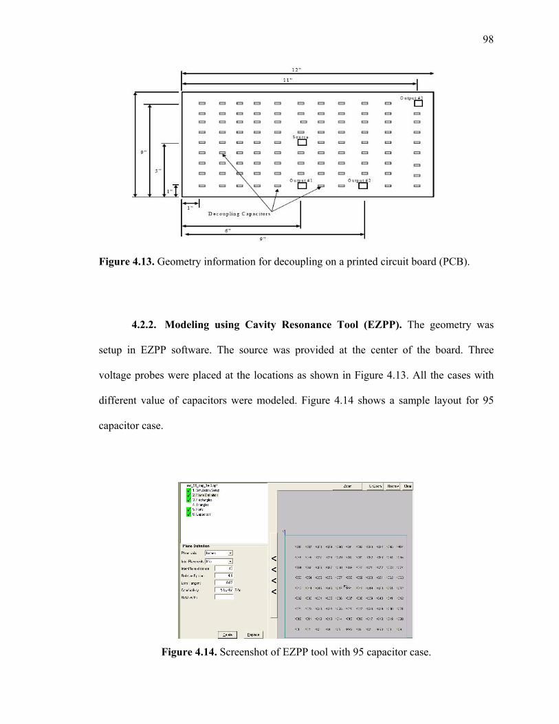
98
Figure 4.13. Geometry information for decoupling on a printed circuit board (PCB).
4.2.2. Modeling using Cavity Resonance Tool (EZPP). The geometry was
setup in EZPP software. The source was provided at the center of the board. Three
voltage probes were placed at the locations as shown in Figure 4.13. All the cases with
different value of capacitors were modeled. Figure 4.14 shows a sample layout for 95
capacitor case.
Figure 4.14. Screenshot of EZPP tool with 95 capacitor case.
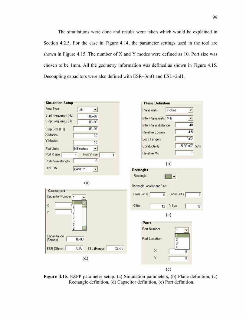
99
The simulations were done and results were taken which would be explained in
Section 4.2.5. For the case in Figure 4.14, the parameter settings used in the tool are
shown in Figure 4.15. The number of X and Y modes were defined as 10. Port size was
chosen to be 1mm. All the geometry information was defined as shown in Figure 4.15.
Decoupling capacitors were also defined with ESR=3mΩ and ESL=2nH.
Figure 4.15. EZPP parameter setup. (a) Simulation parameters, (b) Plane definition, (c)
Rectangle definition, (d) Capacitor definition, (e) Port definition.
(a)
(b)
(d)
(c)
(e)
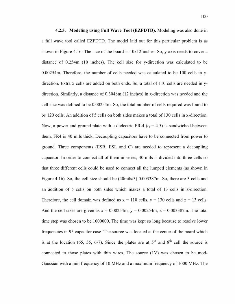
100
4.2.3. Modeling using Full Wave Tool (EZFDTD). Modeling was also done in
a full wave tool called EZFDTD. The model laid out for this particular problem is as
shown in Figure 4.16. The size of the board is 10x12 inches. So, y-axis needs to cover a
distance of 0.254m (10 inches). The cell size for y-direction was calculated to be
0.00254m. Therefore, the number of cells needed was calculated to be 100 cells in y-
direction. Extra 5 cells are added on both ends. So, a total of 110 cells are needed in y-
direction. Similarly, a distance of 0.3048m (12 inches) in x-direction was needed and the
cell size was defined to be 0.00254m. So, the total number of cells required was found to
be 120 cells. An addition of 5 cells on both sides makes a total of 130 cells in x-direction.
Now, a power and ground plate with a dielectric FR-4 (εr = 4.5) is sandwiched between
them. FR4 is 40 mils thick. Decoupling capacitors have to be connected from power to
ground. Three components (ESR, ESL and C) are needed to represent a decoupling
capacitor. In order to connect all of them in series, 40 mils is divided into three cells so
that three different cells could be used to connect all the lumped elements (as shown in
Figure 4.16). So, the cell size should be (40mils/3) 0.003387m. So, there are 3 cells and
an addition of 5 cells on both sides which makes a total of 13 cells in z-direction.
Therefore, the cell domain was defined as x = 110 cells, y = 130 cells and z = 13 cells.
And the cell sizes are given as x = 0.00254m, y = 0.00254m, z = 0.003387m. The total
time step was chosen to be 1000000. The time was kept so long because to resolve lower
frequencies in 95 capacitor case. The source was located at the center of the board which
is at the location (65, 55, 6-7). Since the plates are at 5th and 8th cell the source is
connected to those plates with thin wires. The source (1V) was chosen to be mod-
Gaussian with a min frequency of 10 MHz and a maximum frequency of 1000 MHz. The
101
source type was chosen to be resistive with a resistance of 50ohms. Then, the FR-4 plate
was defined which is 40 mils thick which covers 3 cells in z-direction. The two power
planes are also defined. Voltages are probed at three locations in the plates as shown in
Figure 4.16. A size of a cell is also shown in Figure 4.16.
Figure 4.16. Geometry defined in EZ-FDTD.
EZFDTD requires specification of conductivity of the material instead of
specifying the tan δ. Since loss tangent was used to specify losses in other two tools, it
was a bit of difficulty to match all the Q values. Finally, an approximation was derived to
130 cells
110 cells
Cell Domain
Voltage Probe Location 2
(115, 95, 5-8)
Voltage Probe
Location 3
13 cells
Voltage Probe Location 1
(65, 15, 5-8)
0.003387m
0.00254m
Cell
0.00254m
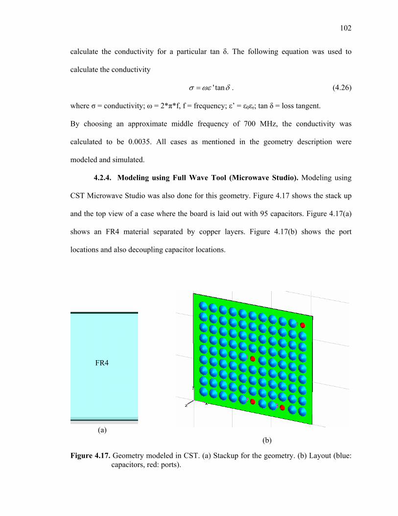
102
calculate the conductivity for a particular tan δ. The following equation was used to
calculate the conductivity
' tanσ ωε δ= . (4.26)
where σ = conductivity; ω = 2*π*f, f = frequency; ε’ = ε0εr; tan δ = loss tangent.
By choosing an approximate middle frequency of 700 MHz, the conductivity was
calculated to be 0.0035. All cases as mentioned in the geometry description were
modeled and simulated.
4.2.4. Modeling using Full Wave Tool (Microwave Studio). Modeling using
CST Microwave Studio was also done for this geometry. Figure 4.17 shows the stack up
and the top view of a case where the board is laid out with 95 capacitors. Figure 4.17(a)
shows an FR4 material separated by copper layers. Figure 4.17(b) shows the port
locations and also decoupling capacitor locations.
Figure 4.17. Geometry modeled in CST. (a) Stackup for the geometry. (b) Layout (blue:
capacitors, red: ports).
FR4
(a) (b)
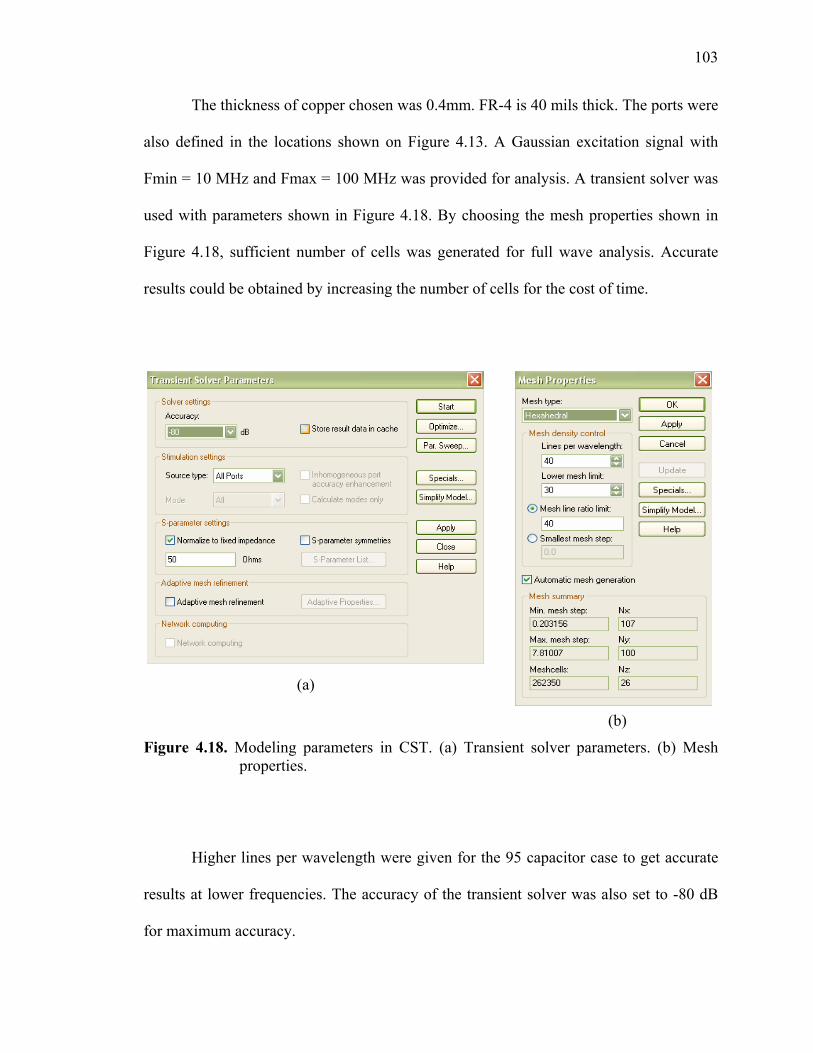
103
The thickness of copper chosen was 0.4mm. FR-4 is 40 mils thick. The ports were
also defined in the locations shown on Figure 4.13. A Gaussian excitation signal with
Fmin = 10 MHz and Fmax = 100 MHz was provided for analysis. A transient solver was
used with parameters shown in Figure 4.18. By choosing the mesh properties shown in
Figure 4.18, sufficient number of cells was generated for full wave analysis. Accurate
results could be obtained by increasing the number of cells for the cost of time.
Figure 4.18. Modeling parameters in CST. (a) Transient solver parameters. (b) Mesh properties.
Higher lines per wavelength were given for the 95 capacitor case to get accurate
results at lower frequencies. The accuracy of the transient solver was also set to -80 dB
for maximum accuracy.
(a)
(b)
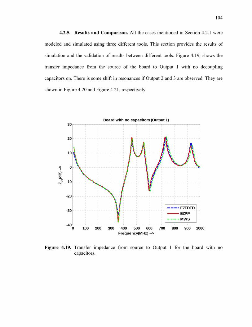
104
4.2.5. Results and Comparison. All the cases mentioned in Section 4.2.1 were
modeled and simulated using three different tools. This section provides the results of
simulation and the validation of results between different tools. Figure 4.19, shows the
transfer impedance from the source of the board to Output 1 with no decoupling
capacitors on. There is some shift in resonances if Output 2 and 3 are observed. They are
shown in Figure 4.20 and Figure 4.21, respectively.
0 100 200 300 400 500 600 700 800 900 1000-40
-30
-20
-10
0
10
20
30Board with no capacitors (Output 1)
Frequency(MHz) -->
Z 21(d
B) --
>
EZFDTDEZPPMWS
Figure 4.19. Transfer impedance from source to Output 1 for the board with no
capacitors.
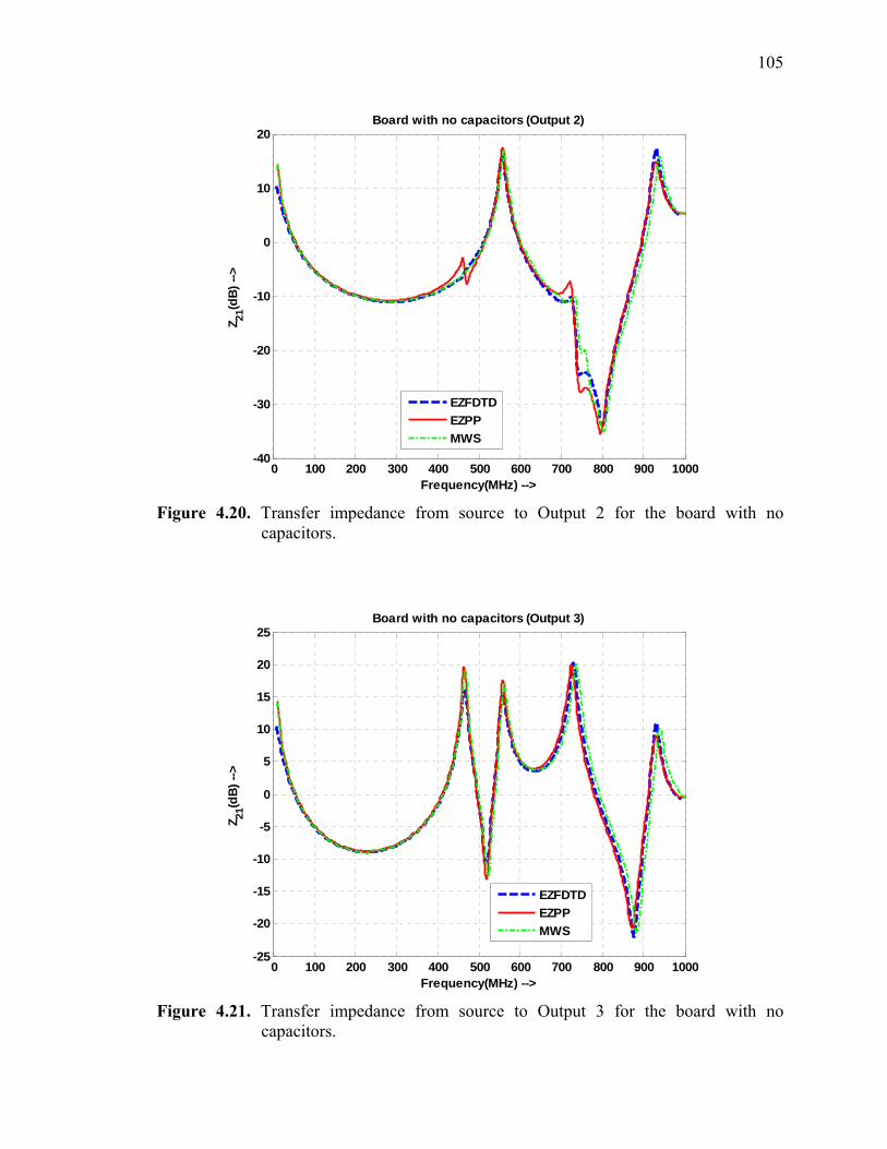
105
0 100 200 300 400 500 600 700 800 900 1000-40
-30
-20
-10
0
10
20Board with no capacitors (Output 2)
Frequency(MHz) -->
Z 21(d
B) --
>
EZFDTDEZPPMWS
Figure 4.20. Transfer impedance from source to Output 2 for the board with no
capacitors.
0 100 200 300 400 500 600 700 800 900 1000-25
-20
-15
-10
-5
0
5
10
15
20
25Board with no capacitors (Output 3)
Frequency(MHz) -->
Z 21(d
B) --
>
EZFDTDEZPPMWS
Figure 4.21. Transfer impedance from source to Output 3 for the board with no
capacitors.
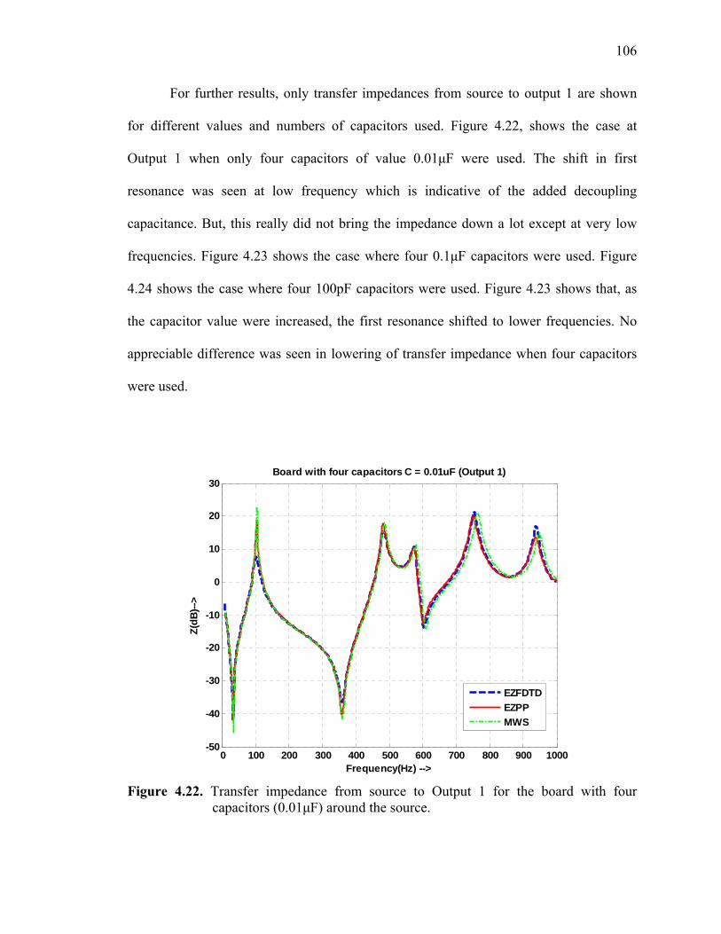
106
For further results, only transfer impedances from source to output 1 are shown
for different values and numbers of capacitors used. Figure 4.22, shows the case at
Output 1 when only four capacitors of value 0.01μF were used. The shift in first
resonance was seen at low frequency which is indicative of the added decoupling
capacitance. But, this really did not bring the impedance down a lot except at very low
frequencies. Figure 4.23 shows the case where four 0.1μF capacitors were used. Figure
4.24 shows the case where four 100pF capacitors were used. Figure 4.23 shows that, as
the capacitor value were increased, the first resonance shifted to lower frequencies. No
appreciable difference was seen in lowering of transfer impedance when four capacitors
were used.
0 100 200 300 400 500 600 700 800 900 1000-50
-40
-30
-20
-10
0
10
20
30Board with four capacitors C = 0.01uF (Output 1)
Frequency(Hz) -->
Z(dB
)-->
EZFDTDEZPPMWS
Figure 4.22. Transfer impedance from source to Output 1 for the board with four
capacitors (0.01μF) around the source.
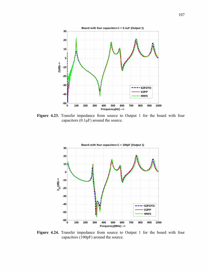
107
0 100 200 300 400 500 600 700 800 900 1000-50
-40
-30
-20
-10
0
10
20
30Board with four capacitors C = 0.1uF (Output 1)
Frequency(Hz) -->
Z(dB
)-->
EZFDTDEZPPMWS
Figure 4.23. Transfer impedance from source to Output 1 for the board with four
capacitors (0.1μF) around the source.
0 100 200 300 400 500 600 700 800 900 1000-60
-50
-40
-30
-20
-10
0
10
20
30Board with four capacitors C = 100pF (Output 1)
Frequency(MHz) -->
Z 21(d
B)--
>
EZFDTDEZPPMWS
Figure 4.24. Transfer impedance from source to Output 1 for the board with four
capacitors (100pF) around the source.
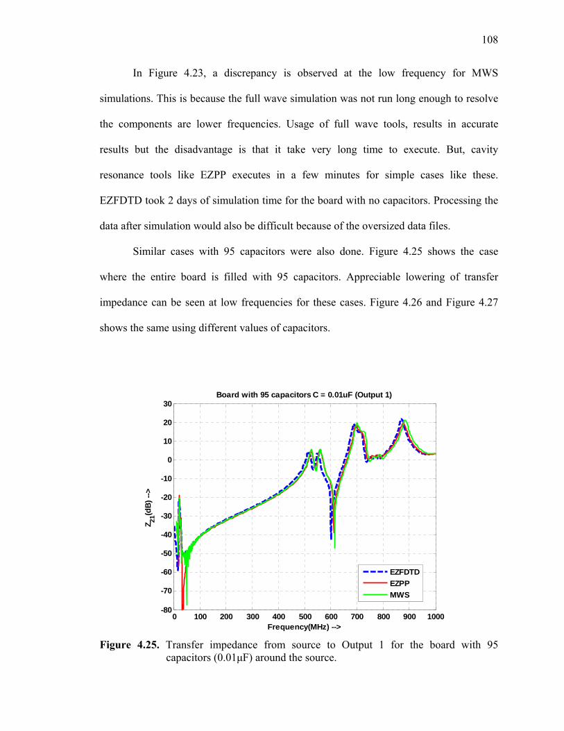
108
In Figure 4.23, a discrepancy is observed at the low frequency for MWS
simulations. This is because the full wave simulation was not run long enough to resolve
the components are lower frequencies. Usage of full wave tools, results in accurate
results but the disadvantage is that it take very long time to execute. But, cavity
resonance tools like EZPP executes in a few minutes for simple cases like these.
EZFDTD took 2 days of simulation time for the board with no capacitors. Processing the
data after simulation would also be difficult because of the oversized data files.
Similar cases with 95 capacitors were also done. Figure 4.25 shows the case
where the entire board is filled with 95 capacitors. Appreciable lowering of transfer
impedance can be seen at low frequencies for these cases. Figure 4.26 and Figure 4.27
shows the same using different values of capacitors.
0 100 200 300 400 500 600 700 800 900 1000-80
-70
-60
-50
-40
-30
-20
-10
0
10
20
30Board with 95 capacitors C = 0.01uF (Output 1)
Frequency(MHz) -->
Z 21(d
B) --
>
EZFDTDEZPPMWS
Figure 4.25. Transfer impedance from source to Output 1 for the board with 95
capacitors (0.01μF) around the source.
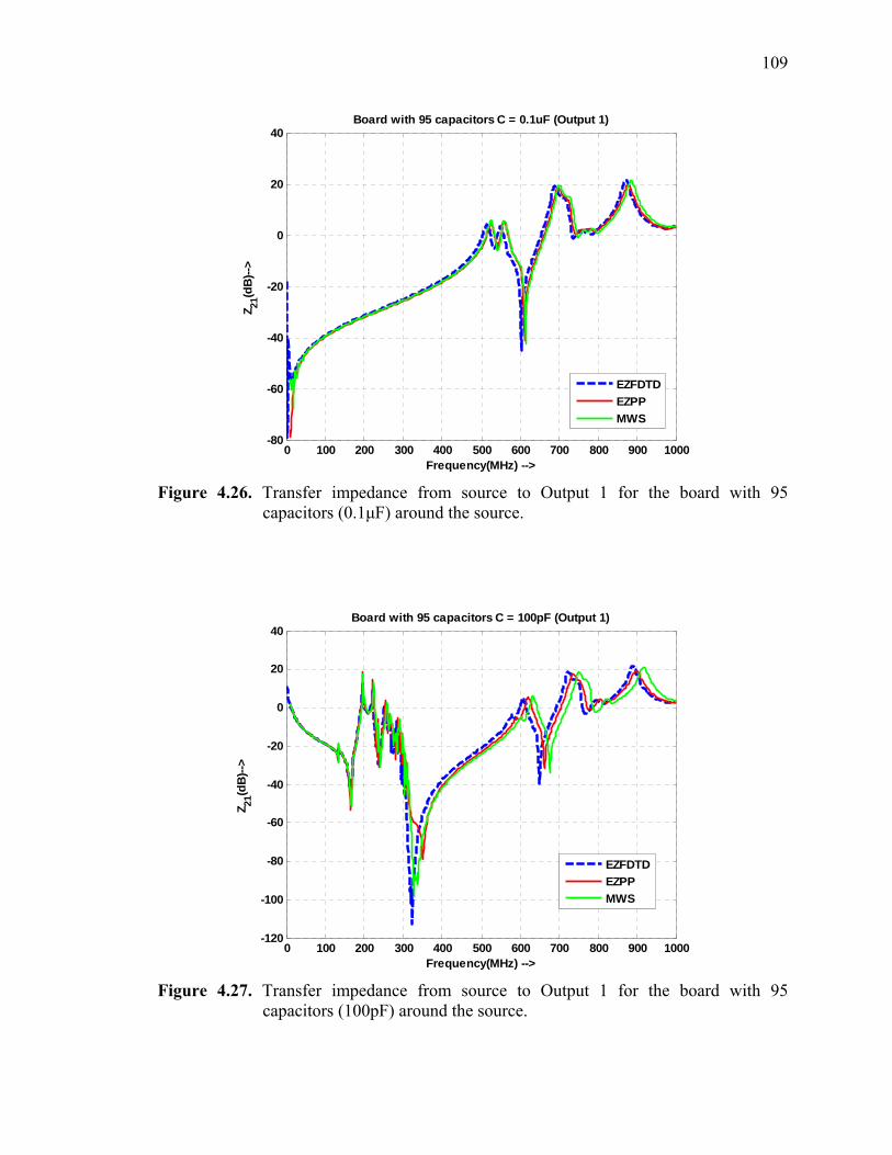
109
0 100 200 300 400 500 600 700 800 900 1000-80
-60
-40
-20
0
20
40Board with 95 capacitors C = 0.1uF (Output 1)
Frequency(MHz) -->
Z 21(d
B)--
>
EZFDTDEZPPMWS
Figure 4.26. Transfer impedance from source to Output 1 for the board with 95
capacitors (0.1μF) around the source.
0 100 200 300 400 500 600 700 800 900 1000-120
-100
-80
-60
-40
-20
0
20
40Board with 95 capacitors C = 100pF (Output 1)
Frequency(MHz) -->
Z 21(d
B)--
>
EZFDTDEZPPMWS
Figure 4.27. Transfer impedance from source to Output 1 for the board with 95
capacitors (100pF) around the source.

110
The use of 95 capacitors works pretty well in reducing the impedance at lower
frequencies. Figure 4.26 shifts lowest resonance to very low frequencies and the
impedance is low up to about 650 MHz. At higher frequencies, the series inductance
(ESL) starts to dominate and take over. So, the decoupling strategies should also be
considering the reduction of the package inductance when the frequency of interest is
high. Studies of this sort are very important when considering power integrity issues. It
becomes very important to supply enough charge for switching the transistors in digital
devices. Otherwise the device will fail to operate.
111
5. SUMMARY The material extraction procedure for a stripline geometry was refined using two
sample test boards. A measurement protocol was developed to be applied for microstrip
test vehicles. Two different techniques were developed to extract material parameters
from microstrip transmission lines. A new microstrip test board was designed. Several
variants of FR-4 samples were manufactured from different printed circuit board (PCB)
suppliers. All samples were measured and material parameters were extracted.
RIE loss was analytically shown to be a potential standard for loss
characterization. Stripline test boards were used to characterize losses. Measurements
were done in both the frequency-domain and time-domain. RIE loss numbers were
extracted and compared. Calculated RIE loss numbers were also obtained for
comparison. The comparison proved that the numbers from TDR measurements agree to
numbers from VNA measurements with about 12% of accuracy.
Propagation delay through a dielectric slap was analyzed analytically. EZFDTD
and PSpice were used to model the geometry and validate the calculated results. A large
PCB was modeled with decoupling capacitors to study effects of decoupling on the
reduction of impedance. The usage of a large number of capacitors spread across the
board was adequate to reduce the impedance to an acceptable level at lower frequencies.
The results were validated using three different CAD tools.
112
BIBLIOGRAPHY
[1] J. Zhang, J.L. Drewniak, D.J. Pommerenke, R.E. DuBroff, Y. Zhiping, W. Cheng; J. Fisher, S. Camerlo, “Signal link-path characterization up to 20 GHz based on a stripline structure,” Electromagnetic Compatibility, 2006. EMC 2006. 2006 IEEE International Symposium, Vol.2, Iss., 14-18 Aug. 2006 Pages: 356- 361
[2] J. Baker-Jarvis, M. Janezic, B.Riddle, C. Holloway, N.Paulter, J.Blendell,
“Dielectric and conductor-loss characterization and measurements on electronic packaging materials”, NIST Technical Note 1520, Boulder, CO: NIST, USA, July, 2001.
[3] J. Abdulnour, C. Akyel, and K. Wu, “A generic approach for permittivity
measurement of dielectric materials using a discontinuity in a rectangular waveguide or a microstrip line,” IEEE Trans. Microwave Theory Tech., vol. MTT-43, pp. 1060-1066, May 1995.
[4] J. Huang, K. Wu, and C. Akyel, “Characterization of highly dispersive materials
using composite coaxial cells: electromagnetic analysis and wideband measurement,” IEEE Trans. Microwave Theory Tech., vol. MTT-44, pp. 770-777, May 1996.
[5] H. Yue, K. L. Virga, “Dielectric constant and loss tangent measurement using a
stripline fixture,” IEEE Trans. Comp.,Packag., Manufact., Technol-part B., vol. 21, pp. 441-446, Nov. 1998.
[6] M. N. Afsar, J. B. Birch, R. N. Clarke “The Measurement of the Properties of
Materials,” Proc. IEEE, vol. 74, 1, pp. 183-199. , January, 1986
[7] D. M. Pozar, Microwave Engineering, 2
nd edition, New York, John Wiley and
Sons, Inc. 1998. [8] J. Loyer, R. Kunze and X. Ye, “Fiber Weave Effect: Practical Impact Analysis
and Mitigation Strategies,” Proceedings of DesignCon 2007. [9] R.A. Pucel, D.J. Masse, C.P. Hartwig, “Losses in Microstrip,” IEEE Transactions
on Microwave Theory and Techniques. 16(6), pp. 342-350, June 1968. [10] F. Gardiol, Microstrip Circuits, New York, John Wiley and Sons, Inc. 1994. [11] J. Zhang, “Reconstruction of the parameters of Debye and Lorentzian dispersive
media using a genetic algorithm and features and applications of EZ-FDTD,” Ph.D. diss., University of Missouri, Rolla, 2007.
113
[12] M.V. Schneider, “Dielectric loss in hybrid integrated circuits,” Proc.IEEE, pp. 1206–1207, June 1969.
[13] J. Zhang, M.Y. Koledintseva, G. Antonini, K.N. Rozanov, J.L. Drewniak, and A.
Orlandi, “Reconstruction of the parameters of Debye and Lorentzian dispersive media using a genetic algorithm,” Proc. IEEE EMC Symposium, Boston, TX, vol. 2, pp. 898-903, August 18-22, 2003.
[14] J. Knighten, B. Archambeault, J. Fan, G. Selli, S. Connor, J. Drewniak, “PDN
Design Strategies: I. Ceramic SMT Decoupling Capacitors – What Values Should I Choose?,” IEEE EMC Society Newsletter, Issue No. 207, pp. 46-53, Fall 2005.
[15] J. Knighten, B. Archambeault, J. Fan, G. Selli, L. Xue, S. Connor, J. Drewniak,
“PDN Design Strategies: II. Ceramic SMT Decoupling Capacitors – Does Location Matter?,” IEEE EMC Society Newsletter, Issue No. 208, pp. 56-67, Winter 2006.
[16] Knighten, J., B. Archambeault, J. Fan, G. Selli, L. Xue, S. Connor, J. Drewniak,
“PDN Design Strategies: III. Planes and Materials – Are They Important Factors in Power Bus Design?,” IEEE EMC Society Newsletter, Issue No. 210, pp. 58-69, Fall 2006.
[17] Knighten, J., B. Archambeault, J. Fan, G. Selli, A. Rajagopal, S. Connor, J.
Drewniak, “PDN Design Strategies: IV. Sources of PDN Noise,” IEEE EMC Society Newsletter, Issue No. 212, pp. 66-76, Winter 2007.
114
VITA
Abhilash Rajagopal was born in Trivandrum, India on October 31st 1981. He
received his B.E. degree in Electronics and Communication Engineering from
Bharathiyar University, Tamilnadu, India, in 2003 and received his M.S. degree in
Electrical Engineering at the University of Missouri-Rolla in May 2006. He was a
graduate research assistant in the Electromagnetic Compatibility Laboratory, University
of Missouri-Rolla. He is received his second M.S degree in Computer Engineering at the
University of Missouri-Rolla in December 2007.
Recommended