UCC28089
SLUS623A -- SEPTEMBER 2004 -- REVISED AUGUST 2006
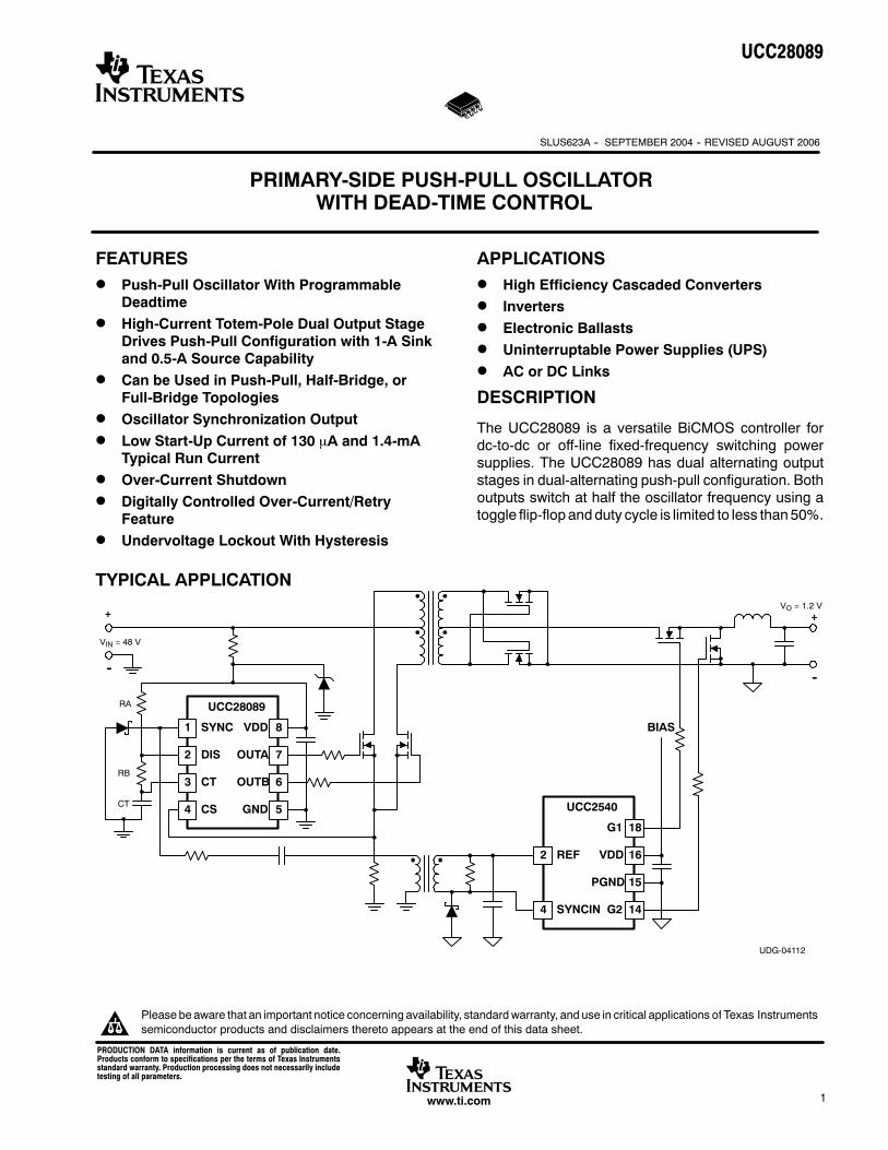
PRIMARY-SIDE PUSH-PULL OSCILLATORWITH DEAD-TIME CONTROL
1www.ti.com
FEATURESD Push-Pull Oscillator With Programmable
DeadtimeD High-Current Totem-Pole Dual Output Stage
Drives Push-Pull Configuration with 1-A Sinkand 0.5-A Source Capability
D Can be Used in Push-Pull, Half-Bridge, orFull-Bridge Topologies
D Oscillator Synchronization Output
D Low Start-Up Current of 130 μA and 1.4-mATypical Run Current
D Over-Current ShutdownD Digitally Controlled Over-Current/Retry
FeatureD Undervoltage Lockout With Hysteresis
APPLICATIONSD High Efficiency Cascaded ConvertersD Inverters
D Electronic BallastsD Uninterruptable Power Supplies (UPS)
D AC or DC Links
DESCRIPTION
The UCC28089 is a versatile BiCMOS controller fordc-to-dc or off-line fixed-frequency switching powersupplies. The UCC28089 has dual alternating outputstages in dual-alternating push-pull configuration. Bothoutputs switch at half the oscillator frequency using atoggle flip-flop andduty cycle is limited to less than50%.
TYPICAL APPLICATION
2
1
4
3
7
8
5
6
UCC28089
SYNC
DIS
CT
CS
VDD
OUTA
OUTB
GND
+
--
2
4
18
UCC2540
REF
SYNCIN
G1
15
16
14
VDD
PGND
G2
--
BIAS
UDG-04112
RA
RB
CT
VIN = 48 V
VO = 1.2 V+
Please be aware that an important notice concerning availability, standardwarranty, and use in critical applications of Texas Instrumentssemiconductor products and disclaimers thereto appears at the end of this data sheet.
PRODUCTION DATA information is current as of publication date.Products conform to specifications per the terms of Texas Instrumentsstandard warranty. Production processing does not necessarily includetesting of all parameters.

UCC28089
SLUS623A -- SEPTEMBER 2004 -- REVISED AUGUST 2006
2 www.ti.com
DESCRIPTION (CONTINUED)
TheUCC28089 is optimized for use as the primary-side companion controller for a cascaded converter that hassecondary-side control. The device incorporates dead-time programming. The synchronization output alsoprovides dead-time information. The retry and soft-start duration scales with the oscillator clock frequency forhigh performance fault recovery.
TheUCC28089 also provides primary side under-voltage protection (UVLO), and over-current protection. Boththe soft start and retry after fault durations scale with oscillator frequency for high performance. The turn-on/offUVLO thresholds are 10.5 V/8.0 V.
ORDERING INFORMATION
TEMPERATURE RANGE PACKAGED DEVICESTEMPERATURE RANGETA = TJ SOIC--8 (D)
--40°C to 105°C UCC28089D† D (SOIC--8) package is available taped and reeled. Add R suffix to device type (e.g. UCC28089DR) to order quantities of 2,500 devices per reel(for D).
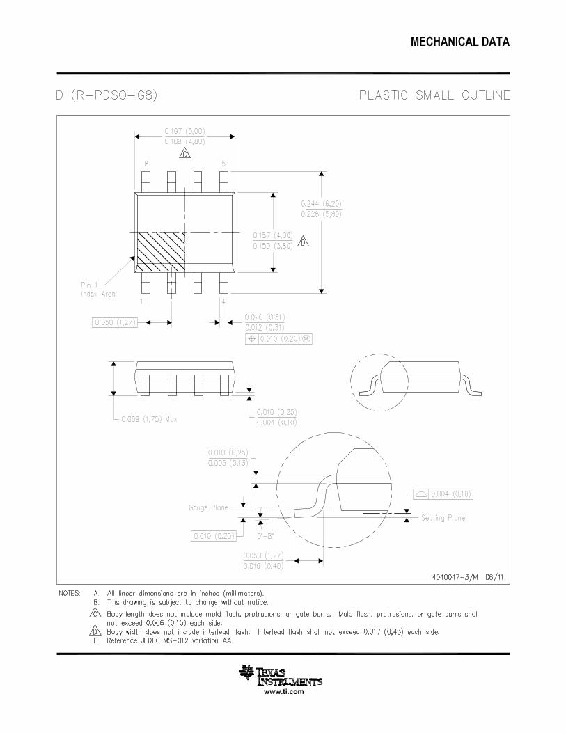
CONNECTION DIAGRAM
1
2
3
4
8
7
6
5
SYNCDISCTCS
VDDOUTAOUTBGND
D PACKAGE (SOIC--8)(TOP VIEW)

UCC28089
SLUS623A -- SEPTEMBER 2004 -- REVISED AUGUST 2006
3www.ti.com
ABSOLUTE MAXIMUM RATINGSover operating free-air temperature (unless otherwise noted)†
PARAMETER SYMBOL RATING UNITS
Supply voltage (IDD < 10 mA) VDD 15 V
Supply current IDD 20 mA
OUTA/OUTB sink current (peak) IOUT(sink) 1.0A
OUTA/OUTB source current (peak) IOUT(source) --0.5A
SYNC sink current (peak) 50mA
SYNC source current (peak) --50mA
Analog inputs (DIS, CT, CS) --0.3 to VDD + 0.3, not to exceed 5 V
Power dissipation at TA = 25°C (D package) 650mW
Power dissipation at TA = 25°C (DRB package) TBDmW
Junction operating temperature TJ --55 to 150
Storage temperature Tstg --65 to 150 oC
Lead temperature (soldering, 10 sec.) Tsol +300
C
† Stresses beyond those listed under “absolutemaximum ratings”may cause permanent damage to the device. These are stress ratings only, andfunctional operation of the device at these or any other conditions beyond those indicated under “recommended operating conditions” is notimplied. Exposure to absolute--maximum--rated conditions for extended periods may affect device reliability.
‡ All voltages arewith respect toGND.Currents are positive into, negative out of the specified terminal. Consult PackagingSection of theDatabookfor thermal limitations and considerations of packages.
RECOMMENDED OPERATION CONDITIONSParameter Symbol MIN TYP MAX UNITS
Supply voltage (IDD < 10 mA) VDD 8.5 14 V
SYNC sink current (peak) 0 10 25mA
SYNC source current (peak) --25 --10 0mA
Analog inputs (DIS, CT, CS) 0 4 V
Timing capacitor range CT 100 100,000 pF
Timing charge resistor range RA 32 750kΩ
Discharge resistor range RB 0 250kΩ
Timing charge current ICHG(RA+RB) 10 300 μA
Switching Frequency fSW 1000 kHz
Junction temperature TJ --40 105 °C
UCC28089
SLUS623A -- SEPTEMBER 2004 -- REVISED AUGUST 2006
4 www.ti.com
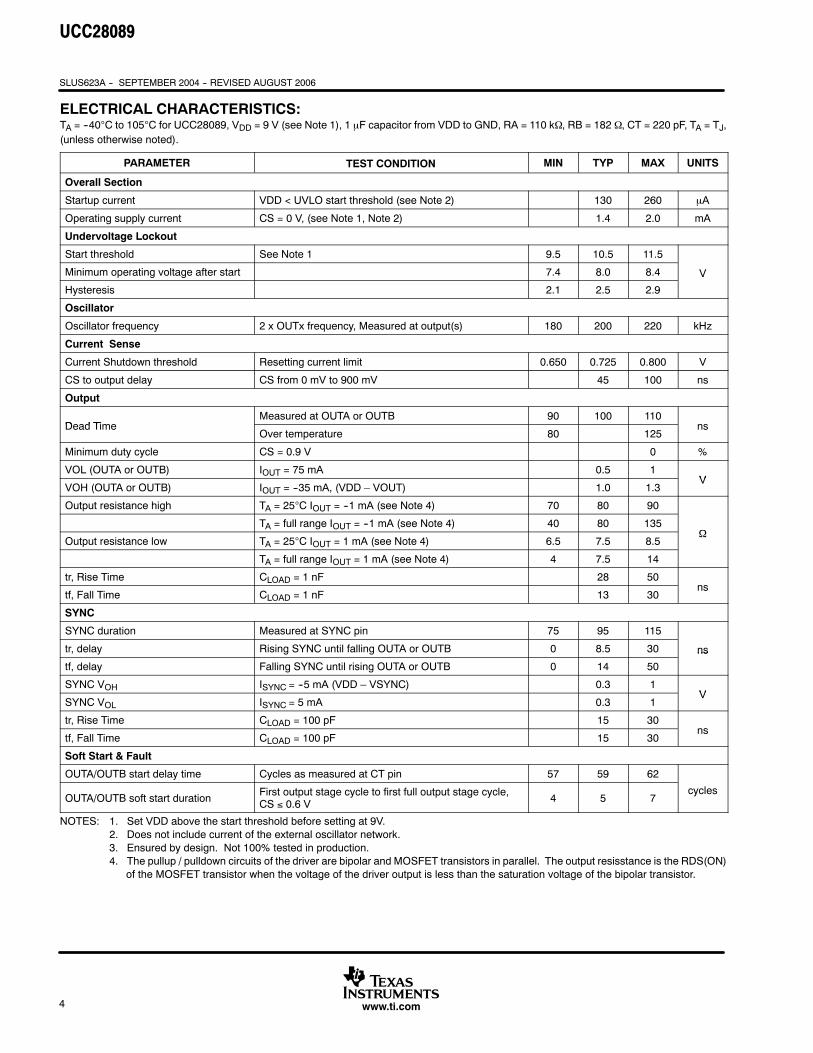
ELECTRICAL CHARACTERISTICS:TA = --40°C to 105°C for UCC28089, VDD = 9 V (see Note 1), 1 μF capacitor from VDD to GND, RA = 110 kΩ, RB = 182 Ω, CT = 220 pF, TA = TJ,(unless otherwise noted).
PARAMETER TEST CONDITION MIN TYP MAX UNITS
Overall Section
Startup current VDD < UVLO start threshold (see Note 2) 130 260 μA
Operating supply current CS = 0 V, (see Note 1, Note 2) 1.4 2.0 mA
Undervoltage Lockout
Start threshold See Note 1 9.5 10.5 11.5
Minimum operating voltage after start 7.4 8.0 8.4 V
Hysteresis 2.1 2.5 2.9
V
Oscillator
Oscillator frequency 2 x OUTx frequency, Measured at output(s) 180 200 220 kHz
Current Sense
Current Shutdown threshold Resetting current limit 0.650 0.725 0.800 V
CS to output delay CS from 0 mV to 900 mV 45 100 ns
Output
Dead TimeMeasured at OUTA or OUTB 90 100 110
nsDead TimeOver temperature 80 125
ns
Minimum duty cycle CS = 0.9 V 0 %
VOL (OUTA or OUTB) IOUT = 75 mA 0.5 1V
VOH (OUTA or OUTB) IOUT = --35 mA, (VDD – VOUT) 1.0 1.3V
Output resistance high TA = 25°C IOUT = --1 mA (see Note 4) 70 80 90
TA = full range IOUT = --1 mA (see Note 4) 40 80 135Ω
Output resistance low TA = 25°C IOUT = 1 mA (see Note 4) 6.5 7.5 8.5Ω
TA = full range IOUT = 1 mA (see Note 4) 4 7.5 14
tr, Rise Time CLOAD = 1 nF 28 50ns
tf, Fall Time CLOAD = 1 nF 13 30ns
SYNC
SYNC duration Measured at SYNC pin 75 95 115
tr, delay Rising SYNC until falling OUTA or OUTB 0 8.5 30 ns
tf, delay Falling SYNC until rising OUTA or OUTB 0 14 50
ns
SYNC VOH ISYNC = --5 mA (VDD – VSYNC) 0.3 1V
SYNC VOL ISYNC = 5 mA 0.3 1V
tr, Rise Time CLOAD = 100 pF 15 30ns
tf, Fall Time CLOAD = 100 pF 15 30ns
Soft Start & Fault
OUTA/OUTB start delay time Cycles as measured at CT pin 57 59 62
OUTA/OUTB soft start durationFirst output stage cycle to first full output stage cycle,CS ≤ 0.6 V 4 5 7
cycles
NOTES: 1. Set VDD above the start threshold before setting at 9V.2. Does not include current of the external oscillator network.3. Ensured by design. Not 100% tested in production.4. The pullup / pulldown circuits of the driver are bipolar and MOSFET transistors in parallel. The output resisstance is the RDS(ON)
of the MOSFET transistor when the voltage of the driver output is less than the saturation voltage of the bipolar transistor.

UCC28089
SLUS623A -- SEPTEMBER 2004 -- REVISED AUGUST 2006
5www.ti.com
FUNCTIONAL BLOCK DIAGRAM
OUTPUT LOGIC
UCC28089
6 OUTB
7 OUTA
8 VDD
4CS
2DIS
1SYNC
3CT
5 GND
VDD
UVLO
VDD = 10.5/8.0 V
VDD
OVERCURRENTCOMP
SS LATCH
0.725 V
SSCOMP
Q
Q
S
R
+
0.2V
56 STEPSTARTDELAY
R
GO 7 STEP SOFT--START RAMP
REFGO
VDD/5
S Q
QR
CKVDD/5
VDD/19.6
QT_
Q
SOFT--START & FAULT
OSCILLATOR
UDG-04101
PIN # NAME I/O FUNCTION
1 SYNC OActive when OUTA and OUTB are active, logic LO at all other times such as during under-voltagelock-out and over-current shutdown. When active, SYNC is logic HI (VDD) during the discharge timeof the oscillator and logic LO (GND) at all other times. The pulse occur during the dead time.
2 DIS ISeparate oscillator timing capacitor discharge pin that allows the dead time to be externallyprogrammed.
3 CT I Oscillator timing capacitor connection.
4 CS ICurrent sense pin. An over current shutdown event is triggered when the voltage of this pin risesabove 0.75 V.
5 GND --Ground pin. Analog and digital signals reference this pin and output drivers return current throughthis pin
6 OUTB O Driver output, capable of sinking 1 A and sourcing 0.5 A. OUTB signal alternates with OUTA.
7 OUTA O Driver output, capable of sinking 1 A and sourcing 0.5 A. OUTA signal alternates with OUTB.
8 VDD I Power input connection for this device.
UCC28089
SLUS623A -- SEPTEMBER 2004 -- REVISED AUGUST 2006
6 www.ti.com
APPLICATION INFORMATION
UCC28089 is an alternating dual-driver output oscillator with over-current and under-voltage fault protection.This feature set is ideal as a start-up controller for isolated power systemswhere themajority of control functionsare performed on the secondary side. This device is especially useful for dc link for topologies such as thecascaded buck converter [1], ac link inverter topologies [2], and inexpensive modified square wave inverters.The UCC28089 has a brief 5 to 7 cycle leading-edge modulated soft-start cycle so that it will not interfere withsecondary-side controlled soft start. Both systems with off-line self bias and auxiliary bias supplies are morefault tolerant with the UCC28089 because it consistently responds to a fault with a delay of at least 56 oscillatorcycles before retry.
Detailed Functional Description
VDD: Power input connection for this device. Although quiescent VDD current is very low, total supply currentis higher, depending on OUTA and OUTB current and the programmed oscillator frequency. During faultresponse, the current drops to a lower level because the oscillator is disabled.
In order to avoid noise problems, position a 1-μF ceramic bypass capacitor, connected from VDD to GND, asclose to the chip as possible. The ceramic bypass capacitor is in addition to any energy storage capacitancethat would be used to hold up the VDD voltage during start-up transients.
GND:Ground pin. Analog signals reference this pin and output drivers return current through this pin. For bestresults, use this pin as a local ground point in a star ground configuration.
OUTA and OUTB: Output drivers capable of sinking 1 A and sourcing 0.5 A. The output pulse alternatesbetweenOUTAandOUTB. In addition, a T latch forces the output pulses to alternate in order to reduce flux buildup in a transformer during low duty ratio operation. Each output is capable of driving the gate of a powerMOSFET.
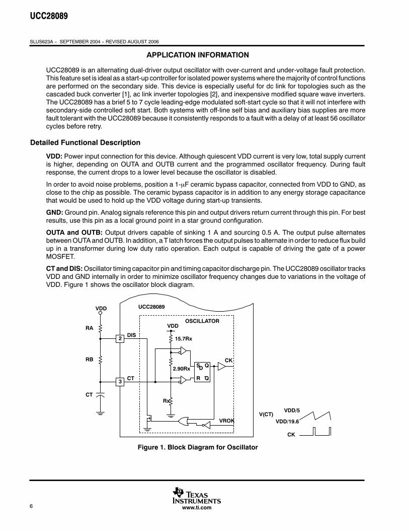
CTandDIS:Oscillator timing capacitor pin and timing capacitor discharge pin. TheUCC28089 oscillator tracksVDD and GND internally in order to minimize oscillator frequency changes due to variations in the voltage ofVDD. Figure 1 shows the oscillator block diagram.
2 DIS
3 CT
RA
RB
CT
VDD
OSCILLATOR
S Q
QR
D
VROK
CK
VDD
15.7Rx
2.90Rx
Rx
UCC28089
VDD/19.6
VDD/5V(CT)
CK
Figure 1. Block Diagram for Oscillator

UCC28089
SLUS623A -- SEPTEMBER 2004 -- REVISED AUGUST 2006
7www.ti.com
APPLICATION INFORMATION
The recommended oscillator frequency range is up to 1 MHz. In order to avoid noise issues, RA and RB shouldbe small enough for the oscillator to have at least 10 μAof current. There are two sets of oscillator programmingequations that model the oscillator over its wide programming range. Measure the charge and the dischargetimes at the SYNC pin in order to avoid affecting the oscillator with probe impedances or output driver delays.
The approximate first order equations in the table are adequate for switching frequencies below 50 kHz and/ordischarge times that are greater than 1 μs. The specific requirements for using the first order equations versusthe second order equations are related to the timing capacitor size and the discharge resistor. Keep inmind thatthe 1st order equations and 2nd order equations are merely approximations that are typically within +/--20% ofthe actual operating point. The frequency, charge and discharge times are relatively insensitive to temperaturebut larger values of CT and RB exhibit the least sensitivity to temperature. Incidentally, the second orderequations apply for the operating conditions that are in the Electrical Characteristics table. The oscillatorfrequency is set according to the following equations:
1ST ORDER EQUATIONS 2ND ORDER EQUATIONS
Condition RA > 300 kΩ AND CT > 300 pF 32 kΩ < RA < 300 kΩ OR 100 pF < CT < 300 pF
TCHARGE 0.169RA+ RBCT 0.175RA+ RB
CT+ 40 pF + 20 ns
TDISCHARGE 1.36 RB CT(1.37)RB+ 44CT+ 14 pF + 20 ns
fOSC 5.9
RA+ 8.0 RBCT
1TCHARGE+ TDISCHARGE
Where RA and RB are in Ohms; CT is in Farads; fOSC is in Hz; tCHARGE and tDISCHARGE are in seconds.
The oscillator is optimized for a CT timing capacitor range from 100 pF to 1000 nF and RB more than 100 Ω.If the shortest discharge time possible is desired, it is permissible to short DIS to CT for all recommended CTvalues (100 pF to 0.100 μF).
SYNC: This SYNC pin produces an output pulse from 0 to VDD that can be used to synchronize a secondaryside-buck controller to the free running isolating power stage. The proper timing of this signal enables zerovoltage switching on the primary side MOSFETs. The clean signal also solves a problem of getting asynchronization signal from the secondary side of the transformer, which can have leakage inductance voltagespikes that may cause false triggering. The SYNC pulse width is the oscillator discharge time, which isapproximately equal to the dead time. Pulse frequency is the oscillator frequency. During fault conditions, theSYNC pulses are terminated and the SYNC output is held low for at least 56 oscillator cycles. During soft start,SYNC precedes the first output pulse by at least one oscillator cycle.
CS:Connect the current sense device to this pin. A voltage threshold of 0.725 V triggers a shutdown sequence.
An over-current fault triggers an immediate shutdown. After the fault clears, a total of 64 oscillator cycles arerequired for an entire soft start sequence to occur. First, the outputs and SYNC are kept OFF for at least 56oscillator cycles. Next, after one or twoSYNCpulses, the soft start progressively increases the output duty ratioover the next five to seven oscillator cycles.

UCC28089
SLUS623A -- SEPTEMBER 2004 -- REVISED AUGUST 2006
8 www.ti.com
APPLICATION INFORMATION
Using the UCC28089 as the Primary-Side start-up Controller in a Cascaded Push-Pull BuckTwo-Stage Converter
The cascaded push-pull topology is ideal for converting from moderate bus voltages, such as 48-V telecombuses, to sub 2-V output voltages. The general topology is shown in Figure 2 using the UCC28089 as theprimary-side start-up controller and the UCC2540 as the secondary-side regulator [3].
UDG-04100
CT
RB
RA10 V
CR1 CR2
VIN = 48 V VO1.2 V
2
1
4
3
7
8
5
6
UCC28089
SYNC
DIS
CT
CS
VDD
OUTA
OUTB
GND
+
--
IN OUT
COM
L.REG
2
1
4
3
19
20
17
18
UCC2540
ISET/SD
REF
G2C
SYNCIN
SWS
BST
G1
SW
6
5
8
7
RAMP
GND
VEA--
CEA--
10
9 COMP
TR
15
16
13
14
VDD
PGND
G2
VDRV
11
12G2S
SS
+
--
Figure 2. Cascaded Push-Pull Buck Two-Stage Converter

UCC28089
SLUS623A -- SEPTEMBER 2004 -- REVISED AUGUST 2006
9www.ti.com
APPLICATION INFORMATION
Program the oscillator frequency of the UCC28089 to equal the desired switching frequency of the output postregulator. The secondary-side controllermayalsoneedcorresponding switching frequencyprogramming, suchas RAMP and G2C capacitor values for the UCC2540. Program the dead time to be approximately 1/4 of theresonant period of the equivalent parasitic L--C circuit that is established by the primary leakage inductance ofthe transformer and the total drain-source capacitance of the primary-side power MOSFET transistors (COSS+stray capacitances).Remember thatCOSSpredictably variesover input line voltage. If the variation is toogreatand/or 1/4 the resonant period is less than 100 ns, connect additional capacitance (CR1 and CR2 in Figure 2)between the drain and source of the primary transistors, which stabilizes the capacitance and raise the totalcapacitance value.
If the secondary-side controller is compatible with pulse edges, the pulse edge transformer circuit in Figure 3can provide an isolated pulse edge signal on the secondary side using a transformer core that is 6-mmdiameteror less.The recommended transformer (COEV#MGBBT--0001101) is compatiblewithall switching frequenciesand it is smaller than many opto-isolators.
UCC28089
R1
634
C1
680 pF
1
5GND
GND1
Primary Ground Secondary Ground
UCC2540
SYNCIN
REFSYNC
4
2
QCL2N3904
T1
1:1
RCB422
RBE115
L1
15uH
Figure 3. Isolation and clamping the SYNC signal for Cascaded Buck Converters
Notice that the peak-pulse voltage is proportional to the UCC28089 bias voltage. The circuit in Figure 3 is wellsuited to the full VDDbias voltage rangeof theUCC28089bias voltagebecause it hasa clampcircuit. Theclampcircuit in Figure 3 (RCB, RBE and QCL) is a VBE clamp rather than a Zener diode. A VBE clamp is used herebecause it has much lower capacitance than typical Zener diodes so that the clamp does not affect the narrow50-ns pulsewidth. The clampmaybe replacedby a single resistor in applications, as in Figure 2,where theVDDbias voltage of the UCC28089 is regulated within a +/--5% window.
UCC28089
SLUS623A -- SEPTEMBER 2004 -- REVISED AUGUST 2006
10 www.ti.com
APPLICATION INFORMATION
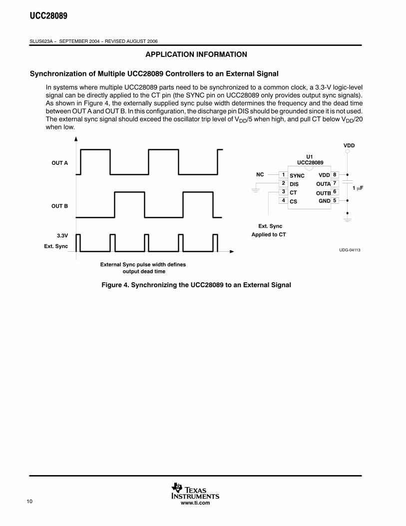
Synchronization of Multiple UCC28089 Controllers to an External Signal
In systems where multiple UCC28089 parts need to be synchronized to a common clock, a 3.3-V logic-levelsignal can be directly applied to the CT pin (the SYNC pin on UCC28089 only provides output sync signals).As shown in Figure 4, the externally supplied sync pulse width determines the frequency and the dead timebetweenOUTAandOUTB. In this configuration, the discharge pinDIS should be grounded since it is not used.The external sync signal should exceed the oscillator trip level of VDD/5 when high, and pull CT below VDD/20when low.
UDG-04113
3.3V
OUT A
OUT B
Ext. Sync
DIS
SYNC
CT
CS GNDOUTB
OUTA
VDD
UCC28089
1
2
3
4 5
6
7
8
Ext. Sync
Applied to CT
U1
External Sync pulse width definesoutput dead time
NC
1 μF
VDD
Figure 4. Synchronizing the UCC28089 to an External Signal

UCC28089
SLUS623A -- SEPTEMBER 2004 -- REVISED AUGUST 2006
11www.ti.com
APPLICATION INFORMATION
Using the UCC28089 as a Modified Square Wave Inverter
Remote or dc-only power systems often require a limited amount of 60-Hz ac line power to supply smallappliances. Compatible loads include universal motors, incandescent lamps, and other electronic devices withswitchedmodepower supplies toconvert the110-VAC to lowerdc voltages.Manyof thesedevicesdonot requirea perfect sinusoidal line voltage, and acceptable performance can be obtained with a modified square wavevoltage. Using the circuit in Figure 5, the UCC28089 can provide the appropriate waveform along with primaryside over-current protection.ComponentsRA,RB, andCTare selected to program thedesiredmodified squarewaveform with the appropriate dead time.
UDG-04105
CT0.1 μF
RB27 kΩ
RA221 kΩ
NC200 Ω
47 μF
12 V BiasVIN = 145 VDC
F1
RS
4.7 μFMPSA42 MPSA42
4.7 μF
--145 V
145 V
0 V
VO110 VAC(rms) 16.7 ms
NOTE: CS signal should be selected to limit peak inrush current to acceptable levels.
1N4003
2
1
4
3
7
8
5
6
UCC28089
SYNC
DIS
CT
CS
VDD
OUTA
OUTB
GND
+
--
6800 pF
6800 pF
50 Ω
200 Ω
200 Ω
50 Ω
200 Ω
20 Ω
Figure 5. Modified Square Wave Inverter
The high-side gate drives of the inverter in Figure 5 are suitable for low frequency applications with relativelyconstant duty ratio. TheNPN transistors and the charge pumpdiodes on the high-side gate drivesmust be ratedfor high voltage (at least 145 V + VDD). The gates are protected from excessive negative voltage by the diodesshown from gate to source.
UCC28089
SLUS623A -- SEPTEMBER 2004 -- REVISED AUGUST 2006
12 www.ti.com
APPLICATION INFORMATION
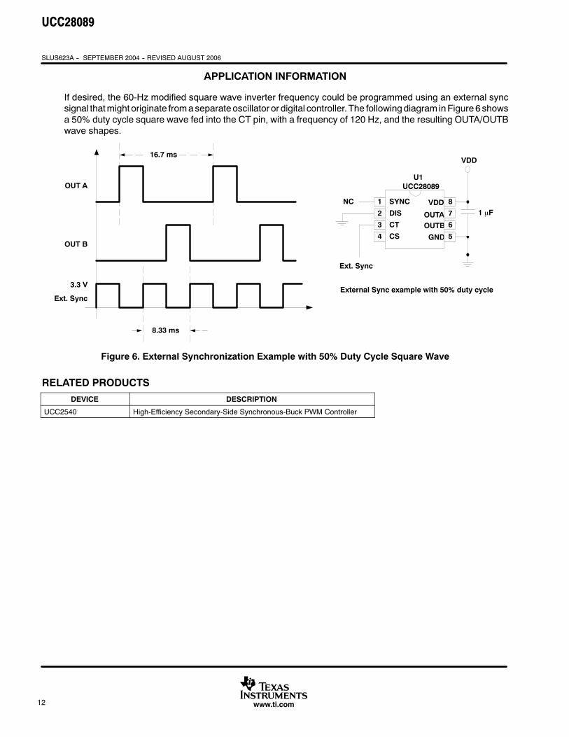
If desired, the 60-Hz modified square wave inverter frequency could be programmed using an external syncsignal thatmight originate fromaseparateoscillator or digital controller. The followingdiagram inFigure6showsa 50% duty cycle square wave fed into the CT pin, with a frequency of 120 Hz, and the resulting OUTA/OUTBwave shapes.
3.3 V
OUT A
OUT B
Ext. Sync
DIS
SYNC
CT
CS GND
OUTBOUTA
VDD
UCC28089
1
2
3
4 5
6
7
8
Ext. Sync
U1
External Sync example with 50% duty cycle
NC
8.33 ms
16.7 msVDD
1 μF
Figure 6. External Synchronization Example with 50% Duty Cycle Square Wave
RELATED PRODUCTS
DEVICE DESCRIPTION
UCC2540 High-Efficiency Secondary-Side Synchronous-Buck PWM Controller

UCC28089
SLUS623A -- SEPTEMBER 2004 -- REVISED AUGUST 2006
13www.ti.com
TYPICAL CHARACTERISTICS
Figure 7
OSCILLATOR FREQUENCYvs
TEMPERATURE
f s--OscillatorFrequency--kH
z
Tj -- Temperature -- °C
--50 50
190
180
25 100750--25
185
195
210
200
205
215
220
RA = 110 kΩRB = 182 ΩCT = 220 pF
Figure 8
Tj -- Temperature -- °C
--50 50 125
98
94
25 100750--25
96
100
106
102
104
108
110
90
92
OSCILLATOR FREQUENCYvs
TEMPERATURE
f s--OscillatorFrequency--kH
z
RA = 221 kΩRB = 3.32 ΩCT = 220 pF
Figure 9
Tj -- Temperature -- °C
--50 50 125
--1.0%
--2.0%
25 100750--25
--1.5%
--0.5%
1.0%
0.0%
0.5%
1.5%
2.0%
OSCILLATOR FREQUENCY SHIFTvs
TEMPERATURE
f s--Norm
alized
to25
°C--kH
z
RA = 110 kΩRB = 182 ΩCT = 220 pF
RA = 221 kΩRB = 3.32 ΩCT = 220 pF
VDD = 9 V
Figure 10
OSCILLATOR FREQUENCY SHIFTvs
SUPPLY VOLTAGE
f--Frequency,N
orm
alized
--%
VDD -- Supply Voltage -- V
8 12 15
0.0%
--0.5%
11 1413109
0.5%
1.5%
1.0%
2.0%RA = 110 kΩRB = 182 ΩCT = 220 pF
RA = 221 kΩRB = 3.32 ΩCT = 220 pF

UCC28089
SLUS623A -- SEPTEMBER 2004 -- REVISED AUGUST 2006
14 www.ti.com
TYPICAL CHARACTERISTICS
Figure 11
OSCILATOR FREQUENCYvs
RA x CT
f OSC--OscilatorFrequensy
--Hz
RA x CT -- s
10 M
1 M
100 K
10 K
1 K
100
1 M
RA = 76.8 kΩRB = 0 ΩVDD = 10 V
10 μ 100 μ1 μ
Figure 12
DISCHARGE TIMEvsCT
Tdischarge--DischargeTime--s
CT-- Farad
100 P 10 n
100 n
10 n
1 n 100 n
RA = 76.8 kΩRB = 0 ΩVDD = 10 V
1 μ
1 μ
10 μ
Figure 13
SYNC PULSE WIDTHvs
TEMPERATURE
SYNC--PulseWidth--ns
Tj -- Temperature -- °C
--50 50 125
85
75
25 100750--25
80
90
105
95
100
110
115
RA = 110 kΩRB = 182 ΩCT = 220 pF
Figure 14
OUTPUT DEAD TIMEvs
TEMPERATURE
T O--OutputDeadTime--ns
Tj -- Temperature -- °C
--50 50 125
95
90
25 100750--25
100
115
105
110
120
125
80
85
RA = 110 kΩRB = 182 ΩCT = 220 pF
UCC28089
SLUS623A -- SEPTEMBER 2004 -- REVISED AUGUST 2006
15www.ti.com
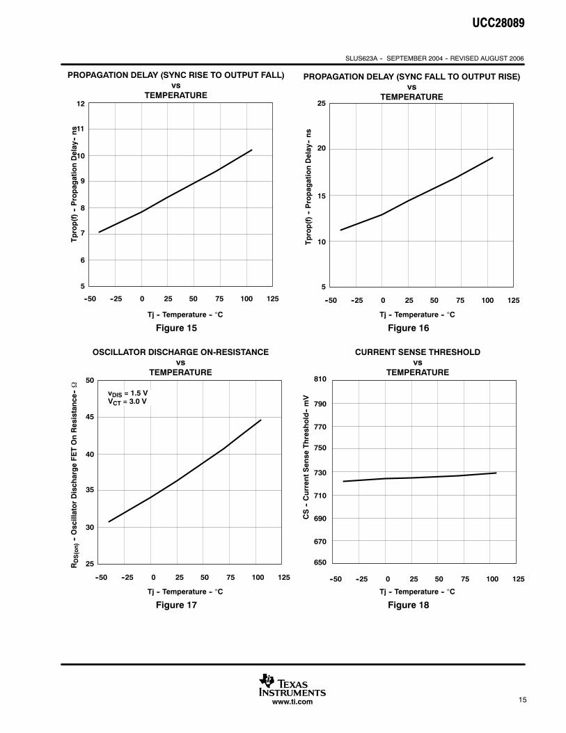
Figure 15
PROPAGATION DELAY (SYNC RISE TO OUTPUT FALL)vs
TEMPERATURE
Tprop(f)--PropagationDelay--ns
Tj -- Temperature -- °C
--50 50 125
7
5
25 100750--25
6
8
11
9
10
12
Figure 16
Tj -- Temperature -- °C
10
5
20
15
25
--50 50 12525 100750--25
PROPAGATION DELAY (SYNC FALL TO OUTPUT RISE)vs
TEMPERATURE
Tprop(f)--PropagationDelay--ns
Figure 17
OSCILLATOR DISCHARGE ON-RESISTANCEvs
TEMPERATURE
RDS(on)--OscillatorDischargeFETOnResistance--Ω
Tj -- Temperature -- °C
50
45
35
30
25
--50 50 12525 100750--25
40
vDIS = 1.5 VVCT = 3.0 V
Figure 18
CURRENT SENSE THRESHOLDvs
TEMPERATURE
CS--CurrentSense
Threshold--mV
Tj -- Temperature -- °C
--50 50 12525 100750--25
810
770
710
690
650
750
670
730
790

UCC28089
SLUS623A -- SEPTEMBER 2004 -- REVISED AUGUST 2006
16 www.ti.com
TYPICAL CHARACTERISTICS
Figure 19
SUPPLY CURRENTvs
OSCILLATOR FREQUENCY (NO LOAD)
IDD--SupplyCurrent--mA
fOSC -- Oscillator Frequency -- kHz
0 600 K 1 M
1.0
800 K400 K200 K
1.5
2.0
3.0
2.5
3.5
4.0
VDD = 14 V
VDD = 12 V
VDD = 9 V
Figure 20
0 600 K 1 M
6
4
400 K 800 K200 K
8
14
10
12
16
18
0
2
SUPPLY CURRENTvs
OSCILLATOR FREQUENCY (1 nF LOADS)
IDD--SupplyCurrent--mA
fOSC -- Oscillator Frequency -- kHz
VDD = 14 V
VDD = 12 V
VDD = 9 V
Figure 21
t -- Time -- 1 ms/div.
OUTA
OUTB
SYNC
CT
TYPICAL SOFT START WAVEFORMS
Figure 22
t -- Time -- 1 ms/div.
OUTA
OUTB
SYNC
CT
TYPICAL OVERALL START--UP WAVEFORMS

UCC28089
SLUS623A -- SEPTEMBER 2004 -- REVISED AUGUST 2006
17www.ti.com
REFERENCES
1. Power Supply Seminar SEM--1300 Topic 1:Unique Cascaded Power Converter Topology for High CurrentLow Output Voltage Applications, by L. Balogh, C. Bridge and B. Andreycak, Texas Instruments LiteratureNo. SLUP133
2. Low Cost Inverter Suitable for Medium-Power Fuel Cell Sources, by P.T. Krein and R Balog, IEEE PowerElectronics Specialists Conference Proceedings, 2002, vol. 1, pp. 321--326.
3. Datasheet, UCC2540 High-Efficiency Secondary-Side Synchronous-Buck PWM Controller, TexasInstruments Literature No. SLUS539

PACKAGING INFORMATION
Orderable Device Status (1) PackageType
PackageDrawing
Pins PackageQty
Eco Plan (2) Lead/Ball Finish MSL Peak Temp (3)
UCC28089D ACTIVE SOIC D 8 75 Green (RoHS &no Sb/Br)
CU NIPDAU Level-1-260C-UNLIM
UCC28089DG4 ACTIVE SOIC D 8 75 Green (RoHS &no Sb/Br)
CU NIPDAU Level-1-260C-UNLIM
UCC28089DR ACTIVE SOIC D 8 2500 Green (RoHS &no Sb/Br)
CU NIPDAU Level-1-260C-UNLIM
UCC28089DRG4 ACTIVE SOIC D 8 2500 Green (RoHS &no Sb/Br)
CU NIPDAU Level-1-260C-UNLIM
(1) The marketing status values are defined as follows:ACTIVE: Product device recommended for new designs.LIFEBUY: TI has announced that the device will be discontinued, and a lifetime-buy period is in effect.NRND: Not recommended for new designs. Device is in production to support existing customers, but TI does not recommend using this part ina new design.PREVIEW: Device has been announced but is not in production. Samples may or may not be available.OBSOLETE: TI has discontinued the production of the device.
(2) Eco Plan - The planned eco-friendly classification: Pb-Free (RoHS), Pb-Free (RoHS Exempt), or Green (RoHS & no Sb/Br) - please checkhttp://www.ti.com/productcontent for the latest availability information and additional product content details.TBD: The Pb-Free/Green conversion plan has not been defined.Pb-Free (RoHS): TI's terms "Lead-Free" or "Pb-Free" mean semiconductor products that are compatible with the current RoHS requirementsfor all 6 substances, including the requirement that lead not exceed 0.1% by weight in homogeneous materials. Where designed to be solderedat high temperatures, TI Pb-Free products are suitable for use in specified lead-free processes.Pb-Free (RoHS Exempt): This component has a RoHS exemption for either 1) lead-based flip-chip solder bumps used between the die andpackage, or 2) lead-based die adhesive used between the die and leadframe. The component is otherwise considered Pb-Free (RoHScompatible) as defined above.Green (RoHS & no Sb/Br): TI defines "Green" to mean Pb-Free (RoHS compatible), and free of Bromine (Br) and Antimony (Sb) based flameretardants (Br or Sb do not exceed 0.1% by weight in homogeneous material)
(3) MSL, Peak Temp. -- The Moisture Sensitivity Level rating according to the JEDEC industry standard classifications, and peak soldertemperature.
Important Information and Disclaimer:The information provided on this page represents TI's knowledge and belief as of the date that it isprovided. TI bases its knowledge and belief on information provided by third parties, and makes no representation or warranty as to theaccuracy of such information. Efforts are underway to better integrate information from third parties. TI has taken and continues to takereasonable steps to provide representative and accurate information but may not have conducted destructive testing or chemical analysis onincoming materials and chemicals. TI and TI suppliers consider certain information to be proprietary, and thus CAS numbers and other limitedinformation may not be available for release.
In no event shall TI's liability arising out of such information exceed the total purchase price of the TI part(s) at issue in this document sold by TIto Customer on an annual basis.
PACKAGE OPTION ADDENDUM
www.ti.com 5-Feb-2007
Addendum-Page 1

TAPE AND REEL INFORMATION
*All dimensions are nominal
Device PackageType
PackageDrawing
Pins SPQ ReelDiameter
(mm)
ReelWidth
W1 (mm)
A0(mm)
B0(mm)
K0(mm)
P1(mm)
W(mm)
Pin1Quadrant
UCC28089DR SOIC D 8 2500 330.0 12.4 6.4 5.2 2.1 8.0 12.0 Q1
PACKAGE MATERIALS INFORMATION
www.ti.com 14-Jul-2012
Pack Materials-Page 1

*All dimensions are nominal
Device Package Type Package Drawing Pins SPQ Length (mm) Width (mm) Height (mm)
UCC28089DR SOIC D 8 2500 367.0 367.0 35.0
PACKAGE MATERIALS INFORMATION
www.ti.com 14-Jul-2012
Pack Materials-Page 2
IMPORTANT NOTICE
Texas Instruments Incorporated and its subsidiaries (TI) reserve the right to make corrections, enhancements, improvements and otherchanges to its semiconductor products and services per JESD46, latest issue, and to discontinue any product or service per JESD48, latestissue. Buyers should obtain the latest relevant information before placing orders and should verify that such information is current andcomplete. All semiconductor products (also referred to herein as “components”) are sold subject to TI’s terms and conditions of salesupplied at the time of order acknowledgment.
TI warrants performance of its components to the specifications applicable at the time of sale, in accordance with the warranty in TI’s termsand conditions of sale of semiconductor products. Testing and other quality control techniques are used to the extent TI deems necessaryto support this warranty. Except where mandated by applicable law, testing of all parameters of each component is not necessarilyperformed.
TI assumes no liability for applications assistance or the design of Buyers’ products. Buyers are responsible for their products andapplications using TI components. To minimize the risks associated with Buyers’ products and applications, Buyers should provideadequate design and operating safeguards.
TI does not warrant or represent that any license, either express or implied, is granted under any patent right, copyright, mask work right, orother intellectual property right relating to any combination, machine, or process in which TI components or services are used. Informationpublished by TI regarding third-party products or services does not constitute a license to use such products or services or a warranty orendorsement thereof. Use of such information may require a license from a third party under the patents or other intellectual property of thethird party, or a license from TI under the patents or other intellectual property of TI.
Reproduction of significant portions of TI information in TI data books or data sheets is permissible only if reproduction is without alterationand is accompanied by all associated warranties, conditions, limitations, and notices. TI is not responsible or liable for such altereddocumentation. Information of third parties may be subject to additional restrictions.
Resale of TI components or services with statements different from or beyond the parameters stated by TI for that component or servicevoids all express and any implied warranties for the associated TI component or service and is an unfair and deceptive business practice.TI is not responsible or liable for any such statements.
Buyer acknowledges and agrees that it is solely responsible for compliance with all legal, regulatory and safety-related requirementsconcerning its products, and any use of TI components in its applications, notwithstanding any applications-related information or supportthat may be provided by TI. Buyer represents and agrees that it has all the necessary expertise to create and implement safeguards whichanticipate dangerous consequences of failures, monitor failures and their consequences, lessen the likelihood of failures that might causeharm and take appropriate remedial actions. Buyer will fully indemnify TI and its representatives against any damages arising out of the useof any TI components in safety-critical applications.
In some cases, TI components may be promoted specifically to facilitate safety-related applications. With such components, TI’s goal is tohelp enable customers to design and create their own end-product solutions that meet applicable functional safety standards andrequirements. Nonetheless, such components are subject to these terms.
No TI components are authorized for use in FDA Class III (or similar life-critical medical equipment) unless authorized officers of the partieshave executed a special agreement specifically governing such use.
Only those TI components which TI has specifically designated as military grade or “enhanced plastic” are designed and intended for use inmilitary/aerospace applications or environments. Buyer acknowledges and agrees that any military or aerospace use of TI componentswhich have not been so designated is solely at the Buyer's risk, and that Buyer is solely responsible for compliance with all legal andregulatory requirements in connection with such use.
TI has specifically designated certain components which meet ISO/TS16949 requirements, mainly for automotive use. Components whichhave not been so designated are neither designed nor intended for automotive use; and TI will not be responsible for any failure of suchcomponents to meet such requirements.
Products Applications
Audio www.ti.com/audio Automotive and Transportation www.ti.com/automotive
Amplifiers amplifier.ti.com Communications and Telecom www.ti.com/communications
Data Converters dataconverter.ti.com Computers and Peripherals www.ti.com/computers
DLP® Products www.dlp.com Consumer Electronics www.ti.com/consumer-apps
DSP dsp.ti.com Energy and Lighting www.ti.com/energy
Clocks and Timers www.ti.com/clocks Industrial www.ti.com/industrial
Interface interface.ti.com Medical www.ti.com/medical
Logic logic.ti.com Security www.ti.com/security
Power Mgmt power.ti.com Space, Avionics and Defense www.ti.com/space-avionics-defense
Microcontrollers microcontroller.ti.com Video and Imaging www.ti.com/video
RFID www.ti-rfid.com
OMAP Applications Processors www.ti.com/omap TI E2E Community e2e.ti.com
Wireless Connectivity www.ti.com/wirelessconnectivity
Mailing Address: Texas Instruments, Post Office Box 655303, Dallas, Texas 75265Copyright © 2012, Texas Instruments Incorporated
Recommended