R
PHY Daughter Card User Guide
For ML32x Development Platforms
UG065 (v1.0) P/N 0402279 May 5, 2004

PHY Daughter Card User Guide www.xilinx.com UG065 (v1.0) P/N 0402279 May 5, 20041-800-255-7778
"Xilinx" and the Xilinx logo shown above are registered trademarks of Xilinx, Inc. Any rights not expressly granted herein are reserved.
CoolRunner, RocketChips, Rocket IP, Spartan, StateBENCH, StateCAD, Virtex, XACT, XC2064, XC3090, XC4005, and XC5210 are registered trademarks of Xilinx, Inc.
The shadow X shown above is a trademark of Xilinx, Inc.
ACE Controller, ACE Flash, A.K.A. Speed, Alliance Series, AllianceCORE, Bencher, ChipScope, Configurable Logic Cell, CORE Generator, CoreLINX, Dual Block, EZTag, Fast CLK, Fast CONNECT, Fast FLASH, FastMap, Fast Zero Power, Foundation, Gigabit Speeds...and Beyond!, HardWire, HDL Bencher, IRL, J Drive, JBits, LCA, LogiBLOX, Logic Cell, LogiCORE, LogicProfessor, MicroBlaze, MicroVia, MultiLINX, NanoBlaze, PicoBlaze, PLUSASM, PowerGuide, PowerMaze, QPro, Real-PCI, RocketIO, SelectIO, SelectRAM, SelectRAM+, Silicon Xpresso, Smartguide, Smart-IP, SmartSearch, SMARTswitch, System ACE, Testbench In A Minute, TrueMap, UIM, VectorMaze, VersaBlock, VersaRing, Virtex-II Pro, Virtex-II EasyPath, Wave Table, WebFITTER, WebPACK, WebPOWERED, XABEL, XACT-Floorplanner, XACT-Performance, XACTstep Advanced, XACTstep Foundry, XAM, XAPP, X-BLOX +, XC designated products, XChecker, XDM, XEPLD, Xilinx Foundation Series, Xilinx XDTV, Xinfo, XSI, XtremeDSP and ZERO+ are trademarks of Xilinx, Inc.
The Programmable Logic Company is a service mark of Xilinx, Inc.
All other trademarks are the property of their respective owners.
Xilinx, Inc. does not assume any liability arising out of the application or use of any product described or shown herein; nor does it convey any license under its patents, copyrights, or maskwork rights or any rights of others. Xilinx, Inc. reserves the right to make changes, at any time, in order to improve reliability, function or design and to supply the best product possible. Xilinx, Inc. will not assume responsibility for the use of any circuitry described herein other than circuitry entirely embodied in its products. Xilinx provides any design, code, or information shown or described herein "as is." By providing the design, code, or information as one possible implementation of a feature, application, or standard, Xilinx makes no representation that such implementation is free from any claims of infringement. You are responsible for obtaining any rights you may require for your implementation. Xilinx expressly disclaims any warranty whatsoever with respect to the adequacy of any such implementation, including but not limited to any warranties or representations that the implementation is free from claims of infringement, as well as any implied warranties of merchantability or fitness for a particular purpose. Xilinx, Inc. devices and products are protected under U.S. Patents. Other U.S. and foreign patents pending. Xilinx, Inc. does not represent that devices shown or products described herein are free from patent infringement or from any other third party right. Xilinx, Inc. assumes no obligation to correct any errors contained herein or to advise any user of this text of any correction if such be made. Xilinx, Inc. will not assume any liability for the accuracy or correctness of any engineering or software support or assistance provided to a user.
Xilinx products are not intended for use in life support appliances, devices, or systems. Use of a Xilinx product in such applications without the written consent of the appropriate Xilinx officer is prohibited.
The contents of this manual are owned and copyrighted by Xilinx. Copyright 1994-2004 Xilinx, Inc. All Rights Reserved. Except as stated herein, none of the material may be copied, reproduced, distributed, republished, downloaded, displayed, posted, or transmitted in any form or by any means including, but not limited to, electronic, mechanical, photocopying, recording, or otherwise, without the prior written consent of Xilinx. Any unauthorized use of any material contained in this manual may violate copyright laws, trademark laws, the laws of privacy and publicity, and communications regulations and statutes.
R

UG065 (v1.0) P/N 0402279 May 5, 2004 www.xilinx.com PHY Daughter Card User Guide1-800-255-7778
PHY Daughter Card User Guide UG065 (v1.0) P/N 0402279 May 5, 2004
The following table shows the revision history for this document..
Version Revision
05/05/04 1.0 Initial Xilinx release.

PHY Daughter Card User Guide www.xilinx.com UG065 (v1.0) P/N 0402279 May 5, 20041-800-255-7778

PHY Daughter Card User Guide www.xilinx.com 5UG065 (v1.0) P/N 0402279 May 5, 2004 1-800-255-7778
R
Preface
About This Guide
This guide documents the PHY daughter card for use with Xilinx ML32x Development Platforms.
Additional ResourcesFor additional information, go to http://support.xilinx.com. The following table lists some of the resources you can access from this website. You can also directly access these resources using the provided URLs.
Resource Description/URL
Tutorials Tutorials covering Xilinx design flows, from design entry to verification and debugging
http://support.xilinx.com/support/techsup/tutorials/index.htm
Answer Browser Database of Xilinx solution records
http://support.xilinx.com/xlnx/xil_ans_browser.jsp
Application Notes Descriptions of device-specific design techniques and approaches
http://support.xilinx.com/apps/appsweb.htm
Data Sheets Device-specific information on Xilinx device characteristics, including readback, boundary scan, configuration, length count, and debugging
http://support.xilinx.com/xlnx/xweb/xil_publications_index.jsp
Problem Solvers Interactive tools that allow you to troubleshoot your design issues
http://support.xilinx.com/support/troubleshoot/psolvers.htm
Tech Tips Latest news, design tips, and patch information for the Xilinx design environment
http://www.support.xilinx.com/xlnx/xil_tt_home.jsp

6 www.xilinx.com PHY Daughter Card User Guide1-800-255-7778 UG065 (v1.0) P/N 0402279 May 5, 2004
Preface: About This GuideR
ConventionsThis document uses the following conventions. An example illustrates each convention.
Online DocumentThe following conventions are used in this document:
Convention Meaning or Use Example
Blue textCross-reference link to a location in the current document
See the section “Additional Resources” for details.
Refer to “Title Formats” in Chapter 1 for details.
Red text Cross-reference link to a location in another document
See Figure 2-5 in the Virtex-II Handbook.
Blue, underlined text Hyperlink to a website (URL) Go to http://www.xilinx.com for the latest speed files.
PHY Daughter Card User Guide www.xilinx.com 7UG065 (v1.0) P/N 0402279 May 5, 2004 1-800-255-7778
R
PHY Daughter Card
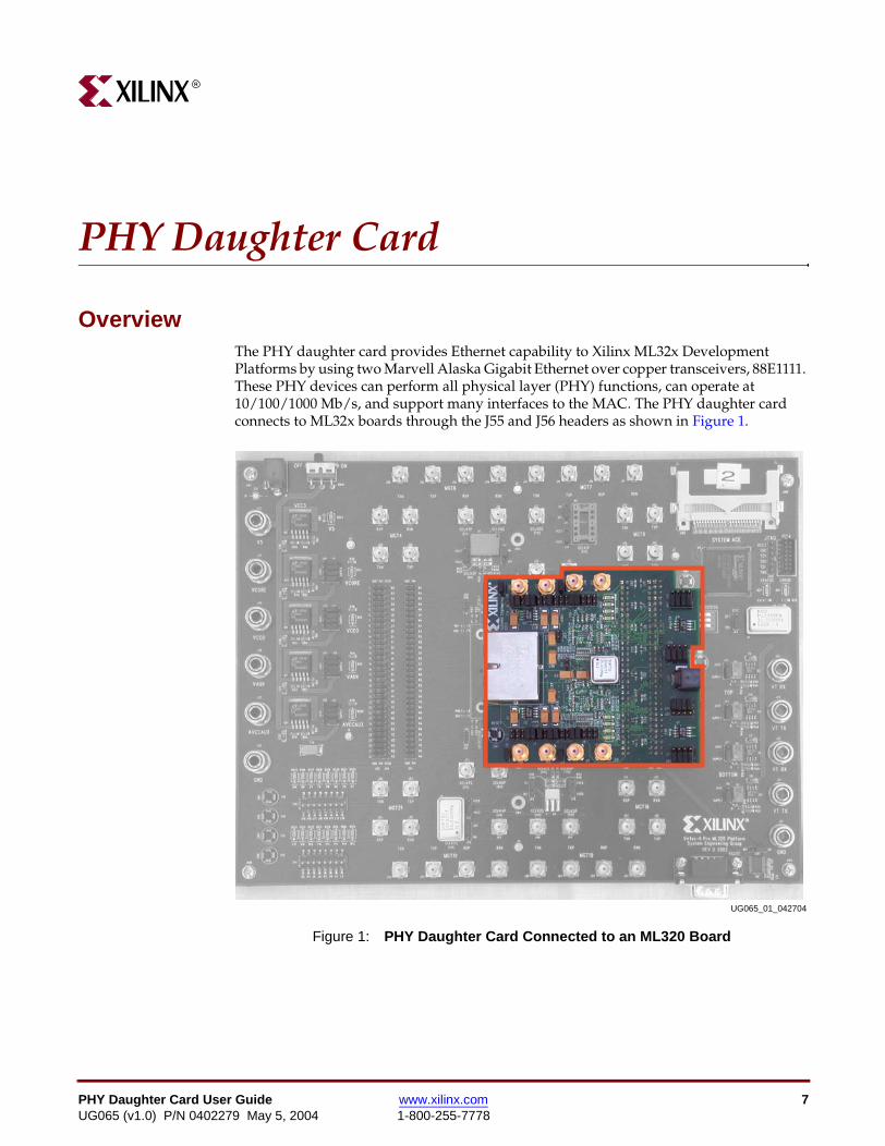
OverviewThe PHY daughter card provides Ethernet capability to Xilinx ML32x Development Platforms by using two Marvell Alaska Gigabit Ethernet over copper transceivers, 88E1111. These PHY devices can perform all physical layer (PHY) functions, can operate at 10/100/1000 Mb/s, and support many interfaces to the MAC. The PHY daughter card connects to ML32x boards through the J55 and J56 headers as shown in Figure 1.
Figure 1: PHY Daughter Card Connected to an ML320 Board
UG065_01_042704

8 www.xilinx.com PHY Daughter Card User Guide1-800-255-7778 UG065 (v1.0) P/N 0402279 May 5, 2004
R
FeaturesThe PHY daughter card features the following:
• Two Marvell Alaska PHY devices (88E1111) with 10/100/1000 Mb/s operation
• Support for the following interfaces:
♦ GMII/MII
♦ SGMII
♦ RGMII
• Two power connection options:
♦ ML32x header pins
♦ 5V external power jack
• Two-port RJ-45 connector
• 2.5V - 25 MHz crystal oscillator for both PHY devices
• SMA connectors for the SGMII interface
Power SettingsThe ML32x PHY daughter card can be powered up either through the VCC pins of the ML32x board when the daughter card is connected to it, or through an external power 5V jack if used on other boards.
To power the daughter card from the VCC pins of the ML32x board through the headers, set the jumpers according to Figure 2.
To power the daughter card from the 5V jack connector, set the jumpers according to Figure 3.
Figure 2: Jumper Settings to Power Up from an ML32x Board
Figure 3: Jumper Settings to Power Up from 5V Jack Connector
UG065_02_043004
J32 J42 J40 J41 J36 J35 J31 J38
J32 J42 J40 J41 J36 J35 J31 J38UG065_03_043004

PHY Daughter Card User Guide www.xilinx.com 9UG065 (v1.0) P/N 0402279 May 5, 2004 1-800-255-7778
Signal ConnectivityR
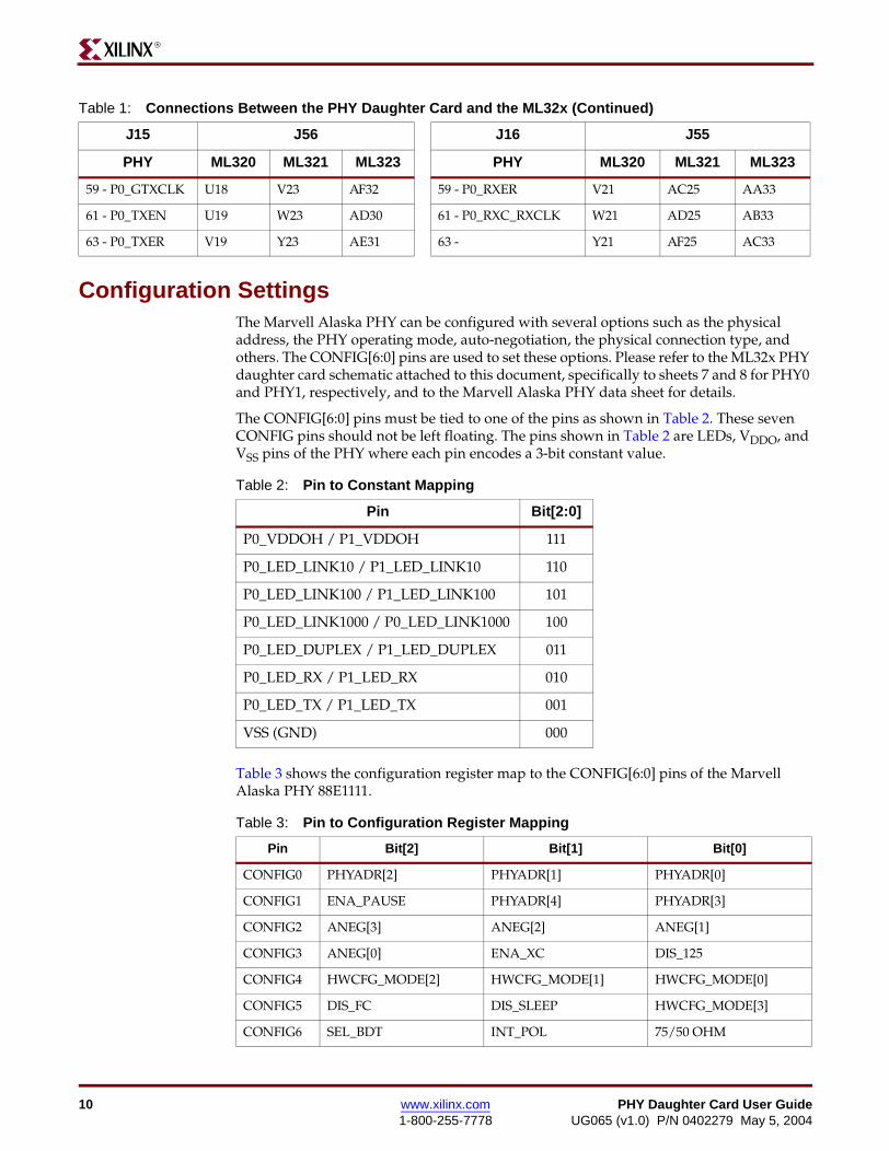
Signal ConnectivityTable 1 shows the signal connections between the PHY daughter card and the ML320, ML321, and ML323 Platforms.
Table 1: Connections Between the PHY Daughter Card and the ML32x
J15 J56 J16 J55
PHY ML320 ML321 ML323 PHY ML320 ML321 ML323
1 - P1_TXD1 E19 E23 K31 1 - D21 A25 N33
3 - P1_TXEN F19 G23 L32 3 - P1_RXC_RXCLK E21 C25 P33
5 - P1_GTXCLK F18 H23 M32 5 - P1_RXD1 F21 D25 R33
7 - P1_COL G19 J23 N32 7 - P1_RXCTL_RXDV G21 E25 T33
9 - P1_TXD3 H19 E24 P32 9 - P1_RCLK1 H21 H25 U33
11 - P1_TXD2 J19 G24 R32 11 - P1_CRS J21 B26 V33
13 - K19 H24 T32 13 - P1_RXER K21 C26 E34
15 - P1_TXD0 L19 J24 U32 15 - P1_RXD7 L21 D26 F30
17 - P1_TXD7 E20 K24 E33 17 - P1_RXD0 D22 E26 L31
19 - P1_TXD6 F20 L24 E31 19 - E22 F26 H34
21 - P1_TXD5 G20 M24 F31 21 - P1_RXD2 F22 G26 K34
23 - P1_TXD4 H20 N24 H33 23 - P1_RXD3 G22 H26 L34
25 - P1_MDC J20 J25 J33 25 - P1_RXD4 H22 J26 M34
27 - P1_MDIO K20 L25 K33 27 - P1_RXD5 J22 K26 N34
29 - P1_TXER L20 M25 L33 29 - P1_RXD6 K22 L26 P34
31 - P1_INT M20 N25 M33 31 - P0_CRS N22 M26 R34
33 - P0_COL N20 P25 AD33 33 - P22 R26 Y34
35 - P0_TXD7 P20 R25 AE33 35 - P0_RXD0 R22 T26 AA34
37 - P0_INT R20 P24 AF33 37 - P0_RXD1 T22 U26 AB34
39 - P0_TXD6 T20 R24 AD31 39 - U22 V26 AC34
41 - P0_TXD5 U20 T24 AH30 41 - P0_RXD2 V22 W26 AD34
43 - P0_TXD4 V20 U24 AK31 43 - W22 Y26 AE34
45 - P0_TXD3 M19 V24 AL33 45 - P0_RXCTL_RXDV Y22 AA26 AG34
47 - P0_TXD2 M18 W24 V32 47 - P0_RXD4 M21 AC26 AD32
49 - P0_TXD1 N19 Y24 W32 49 - P0_RXD5 N21 AD26 AE30
51 - P0_TXD0 P19 AB24 Y32 51 - P0_RXD6 P21 AE26 AK32
53 - P0_MDC R18 AC24 AA32 53 - P0_RXD7 R21 T25 AL34
55 - P0_MDIO R19 AD23 AB32 55 - P0_RCLK1 T21 V25 W33
57 - RESET T19 U23 AC32 57 - P0_RXD3 U21 W25 Y33
10 www.xilinx.com PHY Daughter Card User Guide1-800-255-7778 UG065 (v1.0) P/N 0402279 May 5, 2004
R
Configuration SettingsThe Marvell Alaska PHY can be configured with several options such as the physical address, the PHY operating mode, auto-negotiation, the physical connection type, and others. The CONFIG[6:0] pins are used to set these options. Please refer to the ML32x PHY daughter card schematic attached to this document, specifically to sheets 7 and 8 for PHY0 and PHY1, respectively, and to the Marvell Alaska PHY data sheet for details.
The CONFIG[6:0] pins must be tied to one of the pins as shown in Table 2. These seven CONFIG pins should not be left floating. The pins shown in Table 2 are LEDs, VDDO, and VSS pins of the PHY where each pin encodes a 3-bit constant value.
Table 3 shows the configuration register map to the CONFIG[6:0] pins of the Marvell Alaska PHY 88E1111.
59 - P0_GTXCLK U18 V23 AF32 59 - P0_RXER V21 AC25 AA33
61 - P0_TXEN U19 W23 AD30 61 - P0_RXC_RXCLK W21 AD25 AB33
63 - P0_TXER V19 Y23 AE31 63 - Y21 AF25 AC33
Table 1: Connections Between the PHY Daughter Card and the ML32x (Continued)
J15 J56 J16 J55
PHY ML320 ML321 ML323 PHY ML320 ML321 ML323
Table 2: Pin to Constant Mapping
Pin Bit[2:0]
P0_VDDOH / P1_VDDOH 111
P0_LED_LINK10 / P1_LED_LINK10 110
P0_LED_LINK100 / P1_LED_LINK100 101
P0_LED_LINK1000 / P0_LED_LINK1000 100
P0_LED_DUPLEX / P1_LED_DUPLEX 011
P0_LED_RX / P1_LED_RX 010
P0_LED_TX / P1_LED_TX 001
VSS (GND) 000
Table 3: Pin to Configuration Register Mapping
Pin Bit[2] Bit[1] Bit[0]
CONFIG0 PHYADR[2] PHYADR[1] PHYADR[0]
CONFIG1 ENA_PAUSE PHYADR[4] PHYADR[3]
CONFIG2 ANEG[3] ANEG[2] ANEG[1]
CONFIG3 ANEG[0] ENA_XC DIS_125
CONFIG4 HWCFG_MODE[2] HWCFG_MODE[1] HWCFG_MODE[0]
CONFIG5 DIS_FC DIS_SLEEP HWCFG_MODE[3]
CONFIG6 SEL_BDT INT_POL 75/50 OHM
PHY Daughter Card User Guide www.xilinx.com 11UG065 (v1.0) P/N 0402279 May 5, 2004 1-800-255-7778
Configuration SettingsR
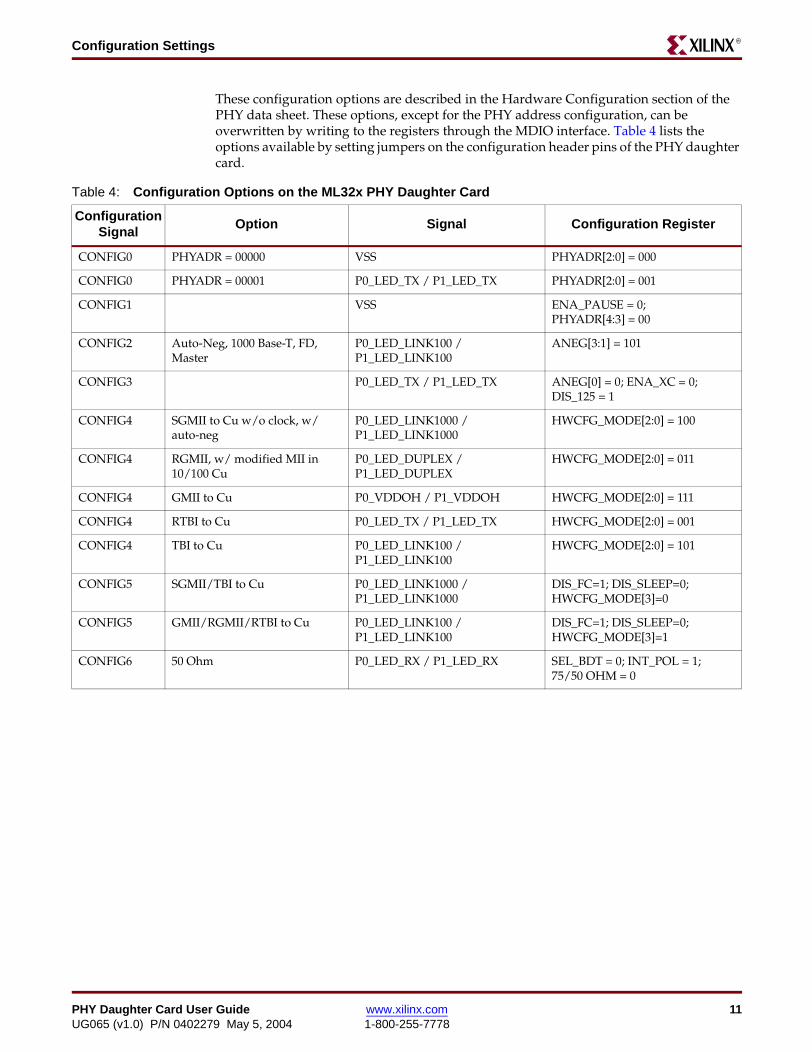
These configuration options are described in the Hardware Configuration section of the PHY data sheet. These options, except for the PHY address configuration, can be overwritten by writing to the registers through the MDIO interface. Table 4 lists the options available by setting jumpers on the configuration header pins of the PHY daughter card.
Table 4: Configuration Options on the ML32x PHY Daughter Card
Configuration Signal
Option Signal Configuration Register
CONFIG0 PHYADR = 00000 VSS PHYADR[2:0] = 000
CONFIG0 PHYADR = 00001 P0_LED_TX / P1_LED_TX PHYADR[2:0] = 001
CONFIG1 VSS ENA_PAUSE = 0;PHYADR[4:3] = 00
CONFIG2 Auto-Neg, 1000 Base-T, FD, Master
P0_LED_LINK100 / P1_LED_LINK100
ANEG[3:1] = 101
CONFIG3 P0_LED_TX / P1_LED_TX ANEG[0] = 0; ENA_XC = 0;DIS_125 = 1
CONFIG4 SGMII to Cu w/o clock, w/ auto-neg
P0_LED_LINK1000 / P1_LED_LINK1000
HWCFG_MODE[2:0] = 100
CONFIG4 RGMII, w/ modified MII in 10/100 Cu
P0_LED_DUPLEX / P1_LED_DUPLEX
HWCFG_MODE[2:0] = 011
CONFIG4 GMII to Cu P0_VDDOH / P1_VDDOH HWCFG_MODE[2:0] = 111
CONFIG4 RTBI to Cu P0_LED_TX / P1_LED_TX HWCFG_MODE[2:0] = 001
CONFIG4 TBI to Cu P0_LED_LINK100 / P1_LED_LINK100
HWCFG_MODE[2:0] = 101
CONFIG5 SGMII/TBI to Cu P0_LED_LINK1000 / P1_LED_LINK1000
DIS_FC=1; DIS_SLEEP=0;HWCFG_MODE[3]=0
CONFIG5 GMII/RGMII/RTBI to Cu P0_LED_LINK100 / P1_LED_LINK100
DIS_FC=1; DIS_SLEEP=0;HWCFG_MODE[3]=1
CONFIG6 50 Ohm P0_LED_RX / P1_LED_RX SEL_BDT = 0; INT_POL = 1;75/50 OHM = 0

12 www.xilinx.com PHY Daughter Card User Guide1-800-255-7778 UG065 (v1.0) P/N 0402279 May 5, 2004
R
GMIITo set the PHY to operate in GMII mode, jumper the configuration headers as illustrated in Figure 4.
Figure 4: Configuration Headers in GMII Mode
J2
PHY 0
J3 J4 J9
J5
2 4 6 8
1 3 5 7
2 4 6 8
1 3 5 7
2 4 6 8
1 3 5 7
2 4 6 8
1 3 5 7
2 4 6 8
1 3 5 7
2 4 6 8
1 3 5 7
2 4 6 8
1 3 5 7
2 4 6 8
1 3 5 7
PHY 1
J6 J7 J10
UG065_04_043004
P0_CONFIG6
P0_CONFIG2
P0_CONFIG1
P0_CONFIG0
P0_CONFIG4
P0_CONFIG3
P0_CONFIG5
P1_CONFIG2
P1_CONFIG1
P1_CONFIG0
P1_CONFIG4
P1_CONFIG3
P1_CONFIG6
P1_CONFIG5

PHY Daughter Card User Guide www.xilinx.com 13UG065 (v1.0) P/N 0402279 May 5, 2004 1-800-255-7778
Configuration SettingsR
Table 5: Configuration Settings for GMII Mode
Configuration Signal
Option Signal Configuration Register
CONFIG0 PHYADR = 00000 VSS PHYADR[2:0] = 000
CONFIG1 VSS ENA_PAUSE = 0;PHYADR[4:3] = 00
CONFIG2 Auto-Neg, 1000 Base-T, FD, Master
P0_LED_LINK100 / P1_LED_LINK100
ANEG[3:1] = 101
CONFIG3 P0_LED_TX / P1_LED_TX ANEG[0] = 0; ENA_XC = 0;DIS_125 = 1
CONFIG4 GMII to Cu P0_VDDOH / P1_VDDOH HWCFG_MODE[2:0] = 111
CONFIG5 GMII/RGMII/RTBI to Cu P0_LED_LINK100 / P1_LED_LINK100
DIS_FC=1; DIS_SLEEP=0;HWCFG_MODE[3]=1
CONFIG6 50 Ohm P0_LED_RX / P1_LED_RX SEL_BDT = 0; INT_POL = 1;75/50 OHM = 0

14 www.xilinx.com PHY Daughter Card User Guide1-800-255-7778 UG065 (v1.0) P/N 0402279 May 5, 2004
R
RGMIITo set the PHY to operate in RGMII mode, jumper the configuration headers as illustrated in Figure 5.
Figure 5: Configuration Headers for RGMII Mode
J2
PHY 0
J3 J4 J9
J5
2 4 6 8
1 3 5 7
2 4 6 8
1 3 5 7
2 4 6 8
1 3 5 7
2 4 6 8
1 3 5 7
2 4 6 8
1 3 5 7
2 4 6 8
1 3 5 7
2 4 6 8
1 3 5 7
2 4 6 8
1 3 5 7
PHY 1
J6 J7 J10
UG065_05_043004
P1_CONFIG2
P1_CONFIG1
P1_CONFIG0
P1_CONFIG4
P1_CONFIG3
P1_CONFIG6
P1_CONFIG5
P0_CONFIG6
P0_CONFIG2
P0_CONFIG1
P0_CONFIG0
P0_CONFIG4
P0_CONFIG3
P0_CONFIG5

PHY Daughter Card User Guide www.xilinx.com 15UG065 (v1.0) P/N 0402279 May 5, 2004 1-800-255-7778
Configuration SettingsR
Table 6: Configuration Settings for RGMII Mode
Configuration Signal
Option Signal Configuration Register
CONFIG0 PHYADR = 00000 VSS PHYADR[2:0] = 000
CONFIG1 VSS ENA_PAUSE = 0; PHYADR[4:3] = 00
CONFIG2 Auto-Neg, 1000 Base-T, FD, Master
P0_LED_LINK100 / P1_LED_LINK100
ANEG[3:1] = 101
CONFIG3 P0_LED_TX / P1_LED_TX ANEG[0] = 0; ENA_XC = 0; DIS_125 = 1
CONFIG4 RGMII, w/ modified MII in 10/100 Cu
P0_LED_DUPLEX / P1_LED_DUPLEX
HWCFG_MODE[2:0] = 011
CONFIG5 GMII/RGMII/RTBI to Cu P0_LED_LINK100 / P1_LED_LINK100
DIS_FC=1; DIS_SLEEP=0; HWCFG_MODE[3]=1
CONFIG6 50 Ohm P0_LED_RX / P1_LED_RX SEL_BDT = 0; INT_POL = 1; 75/50 OHM = 0
16 www.xilinx.com PHY Daughter Card User Guide1-800-255-7778 UG065 (v1.0) P/N 0402279 May 5, 2004
R
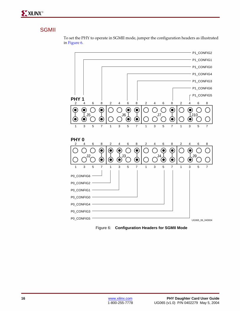
SGMIITo set the PHY to operate in SGMII mode, jumper the configuration headers as illustrated in Figure 6.
Figure 6: Configuration Headers for SGMII Mode
J2
PHY 0
J3 J4 J9
J5
2 4 6 8
1 3 5 7
2 4 6 8
1 3 5 7
2 4 6 8
1 3 5 7
2 4 6 8
1 3 5 7
2 4 6 8
1 3 5 7
2 4 6 8
1 3 5 7
2 4 6 8
1 3 5 7
2 4 6 8
1 3 5 7
PHY 1
J6 J7 J10
UG065_06_043004
P0_CONFIG6
P0_CONFIG2
P0_CONFIG1
P0_CONFIG0
P0_CONFIG4
P0_CONFIG3
P0_CONFIG5
P1_CONFIG2
P1_CONFIG1
P1_CONFIG0
P1_CONFIG4
P1_CONFIG3
P1_CONFIG6
P1_CONFIG5

PHY Daughter Card User Guide www.xilinx.com 17UG065 (v1.0) P/N 0402279 May 5, 2004 1-800-255-7778
Configuration SettingsR
For SGMII operation, connect the SMA connectors of the PHY daughter card to the ML32x MGTs as follows:
• For PHY 1:
♦ J24 to ML32x TXP
♦ J23 to ML32x TXN
♦ J13 to ML32x RXP
♦ J14 to ML32x RXN
• For PHY 0:
♦ J26 to ML32x TXP
♦ J25 to ML32x TXN
♦ J11 to ML32x RXP
♦ J12 to ML32x RXN
Table 7: Configuration Settings for SGMII Mode
Configuration Signal
Option Signal Configuration Register
CONFIG0 PHYADR = 00000 VSS PHYADR[2:0] = 000
CONFIG1 VSS ENA_PAUSE = 0; PHYADR[4:3] = 00
CONFIG2 Auto-Neg, 1000 Base-T, FD, Master
P0_LED_LINK100 / P1_LED_LINK100
ANEG[3:1] = 101
CONFIG3 P0_LED_TX / P1_LED_TX ANEG[0] = 0; ENA_XC = 0; DIS_125 = 1
CONFIG4 SGMII to Cu w/o clock, w/ auto-neg
P0_LED_LINK1000 / P1_LED_LINK1000
HWCFG_MODE[2:0] = 100
CONFIG5 SGMII/TBI to Cu P0_LED_LINK1000 / P1_LED_LINK1000
DIS_FC=1; DIS_SLEEP=0; HWCFG_MODE[3]=0
CONFIG6 50 Ohm P0_LED_RX / P1_LED_RX SEL_BDT = 0; INT_POL = 1; 75/50 OHM = 0

18 www.xilinx.com PHY Daughter Card User Guide1-800-255-7778 UG065 (v1.0) P/N 0402279 May 5, 2004
R
MIITo set either PHY device in 10/100 Mb/s MII mode, the configuration headers for both devices must be connected together. The PHY devices must be set with auto-negotiation for any speed and for duplex capability. The speed and duplex are set by the other end to which the PHY daughter card is connected.
To set PHY 0 to work in MII mode, jumper the configuration headers as illustrated in Figure 7.
Figure 7: Configuration Headers for PHY 0 in MII Mode
J2
PHY 0
J3 J4 J9
J5
2 4 6 8
1 3 5 7
2 4 6 8
1 3 5 7
2 4 6 8
1 3 5 7
2 4 6 8
1 3 5 7
2 4 6 8
1 3 5 7
2 4 6 8
1 3 5 7
2 4 6 8
1 3 5 7
2 4 6 8
1 3 5 7
PHY 1
J6 J7 J10
UG065_07_043004
P0_CONFIG6
P0_CONFIG2
P0_CONFIG1
P0_CONFIG0
P0_CONFIG4
P0_CONFIG3
P0_CONFIG5

PHY Daughter Card User Guide www.xilinx.com 19UG065 (v1.0) P/N 0402279 May 5, 2004 1-800-255-7778
Configuration SettingsR
To set PHY 1 to work in MII mode, jumper the configuration headers as illustrated in Figure 8.
Table 8: Configuration Settings for MII Mode on PHY 0
Configuration Signal
Options Signal Configuration Register
CONFIG0 PHYADR = 00000 VSS PHYADR[2:0] = 000
CONFIG1 VSS ENA_PAUSE = 0; PHYADR[4:3] = 00
CONFIG2 Auto-Neg, all capabilities, Master
P0_VDDOH / P1_VDDOH ANEG[3:1] = 111
CONFIG3 P0_LED_TX / P1_LED_TX ANEG[0] = 0; ENA_XC = 0; DIS_125 = 1
CONFIG4 GMII to Cu P0_VDDOH / P1_VDDOH HWCFG_MODE[2:0] = 111
CONFIG5 GMII/RGMII/RTBI to Cu P0_LED_LINK100 / P1_LED_LINK100
DIS_FC=1; DIS_SLEEP=0; HWCFG_MODE[3]=1
CONFIG6 50 Ohm P0_LED_RX / P1_LED_RX SEL_BDT = 0; INT_POL = 1; 75/50 OHM = 0
Figure 8: Configuration Headers for PHY 1 in MII Mode
J2
PHY 0
J3 J4 J9
J5
2 4 6 8
1 3 5 7
2 4 6 8
1 3 5 7
2 4 6 8
1 3 5 7
2 4 6 8
1 3 5 7
2 4 6 8
1 3 5 7
2 4 6 8
1 3 5 7
2 4 6 8
1 3 5 7
2 4 6 8
1 3 5 7
PHY 1
J6 J7 J10
UG065_08_043004
P1_CONFIG2
P1_CONFIG1
P1_CONFIG0
P1_CONFIG4
P1_CONFIG3
P1_CONFIG6
P1_CONFIG5
20 www.xilinx.com PHY Daughter Card User Guide1-800-255-7778 UG065 (v1.0) P/N 0402279 May 5, 2004
R
References1. Marvell, Marvell Alaska 88E1111 Data Sheet (Available under NDA)
http://www.marvell.com
2. Xilinx, Inc., Virtex-II Pro ML320, ML321, ML323 Platform User Guide
3. IEEE, IEEE Std 802.3, 2002 Edition
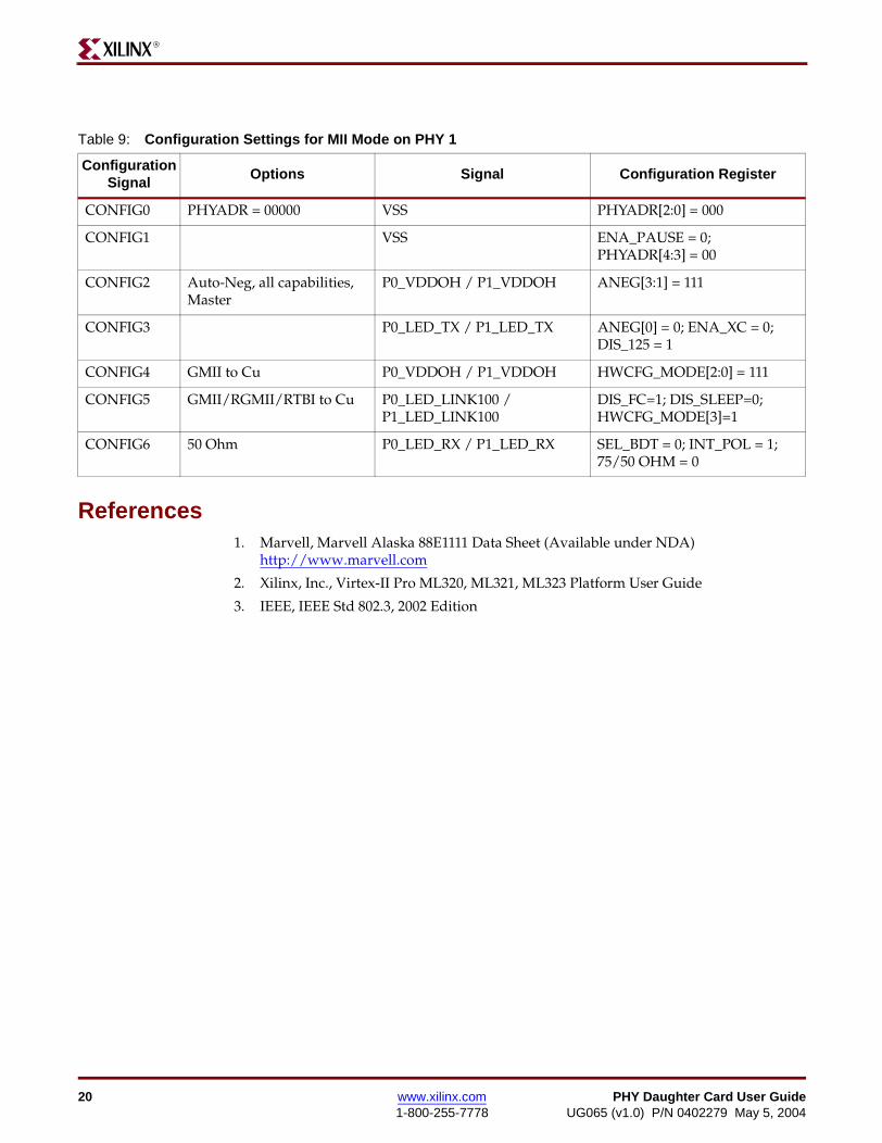
Table 9: Configuration Settings for MII Mode on PHY 1
Configuration Signal
Options Signal Configuration Register
CONFIG0 PHYADR = 00000 VSS PHYADR[2:0] = 000
CONFIG1 VSS ENA_PAUSE = 0; PHYADR[4:3] = 00
CONFIG2 Auto-Neg, all capabilities, Master
P0_VDDOH / P1_VDDOH ANEG[3:1] = 111
CONFIG3 P0_LED_TX / P1_LED_TX ANEG[0] = 0; ENA_XC = 0; DIS_125 = 1
CONFIG4 GMII to Cu P0_VDDOH / P1_VDDOH HWCFG_MODE[2:0] = 111
CONFIG5 GMII/RGMII/RTBI to Cu P0_LED_LINK100 / P1_LED_LINK100
DIS_FC=1; DIS_SLEEP=0; HWCFG_MODE[3]=1
CONFIG6 50 Ohm P0_LED_RX / P1_LED_RX SEL_BDT = 0; INT_POL = 1; 75/50 OHM = 0

ofSheet
Date:
Title:
Ver:A
B
C
D
1234
D
C
B
A
4 3 2 1
Sheet Size: B Rev:
Drawn By
1.0
07/11/03
11
SEG
5 Vdc
AUX_JACK
SNA_CONNECTORS
CONNECTOR
MAGNETICS
Marvell 88E1111
CONFIGURATION/LEDS
BLOCK
AUX GMII SIGNALS
RX GMII SIGNALS
TX GMII SIGNALS
RX RGMII (GMII SUBSET)
TX RGMII (GMII SUBSET)
SGMII_TXD_+/-
SGMII_RXD_+/-
MDI0_+/-
MDI3_+/-
MDI2_+/-
MDI1_+/-
RJ45
SNA_CONNECTORS
CONNECTOR
MAGNETICS
Marvell 88E1111
PHY_0
CONFIGURATION/LEDS
BLOCK
AUX GMII SIGNALS
RX GMII SIGNALS
TX GMII SIGNALS
RX RGMII (GMII SUBSET)
TX RGMII (GMII SUBSET)
SGMII_TXD_+/-
SGMII_RXD_+/-
MDI0_+/-
MDI3_+/-
MDI2_+/-
MDI1_+/-
RJ45 PORT_0
PORT_1
PHY_1
GND
AUX. POWER SUPPLY
1
C
Schematic, PHY Daughter PCB, 1280327
0381166

HDR_2x32HDR_2x32 HDR_1x32
SW-PBUTTON
ofSheet
Date:
Title:
Ver:A
B
C
D
1234
D
C
B
A
4 3 2 1
Sheet Size: B Rev:
Drawn By
Schematic, PHY Daughter PCB, 1280327
0381166
1.0
07/11/03
11
SEG
RESISTERS LOCATED AT 88E1111 PINS
[ML32X_J55] [ML32X_J50](ML32X_J56)
2
C
12
SW1
RESET
26
28
5678910111213141516171819202122232425
293031
27
32
1234
J8
525355 56
1
1011 1213 1415 1617 1819
2
2021 2223 2425 2627 2829
3
3031 3233 3435 3637 3839
4
4041 4243 4445 4647 4849
5
50
67 89
51
63
585759 6061 62
54
64
J15
525355 56
1
1011 1213 1415 1617 1819
2
2021 2223 2425 2627 2829
3
3031 3233 3435 3637 3839
4
4041 4243 4445 4647 4849
5
50
67 89
51
63
585759 6061 62
54
64
J16
P1_COL
P1_TD_TXD0
P1_TD_TXD3
P1_TD_TXD[0:3]
P1_TD_TXD1
P1_TD_TXD2
P0_RXER
12
0
R110
1 2R129
33
12
0
R104
P0_CRS
P0_RXCTL_RXDV
P0_RXC_RXCLK
P0_RXD7
P0_RXD4
P0_RXD5
P0_RXD6
P0_RXD[4:7]
P1_RXC_RXCLK
P1_RCLK1
P1_RXCTL_RXDV
P1_CRS
P1_RXER
P1_RD_RXD[0:3]P1_RD_RXD0
P1_RD_RXD1
P1_RD_RXD3
P1_RD_RXD2
P0_TXER
P0_TXCTL_TXEN
P0_TXC_GTXCLK
P0_RCLK1
P1_TXC_GTXCLK
P1_TXD6
P1_TXD5
P1_TXD4P1_TXD[4:7]
P1_TXD7
P0_TD_TXD0
P0_TD_TXD3
P0_TD_TXD1
P0_TD_TXD[0:3]
P0_TD_TXD2
P0_VDDO
VCCO_CONN
P0_COL
P1_TXER
P1_TXCTL_TXEN
P0_TXD7
P0_TXD5
P0_TXD6
P0_TXD4P0_TXD[4:7]
P1_RXD7
P1_RXD[4:7]
P1_RXD5
P1_RXD4
P1_RXD6
P0_RD_RXD1
P0_RD_RXD0P0_RD_RXD[0:3]
P0_RD_RXD2
P0_RD_RXD3
12
4.7K
R4
1 2R131
331 2
R130
33
1 2R132
33
12
33
R118
1 2R136
33
1 2R140
33
1 2R139
33
1 2R138
33
1 2R137
33
1 2R135
33
1 2R134
33
1 2R133
33
1 2R152
33
1 2R141
33
1 2R143
33
1 2R142
33
1 2R144
33
1 2R145
331 2
R146
331 2
R147
331 2
R148
33
1 2R149
331 2
R150
331 2
R151
33
12
0
R10212
0
R101
12
33
R117
12
0
R11112
0
R112
12
33
R10712
33
R106
12
0
R9912
0
R10012
0
R98
12
0
R96
12
0
R97
12
0
R9512
0
R9412
0
R9312
0
R92
12
0
R109
12
0
R103
1
2
0
R116
1
2
0
R115
1
2
0
R114
1
2
0
R113
12
4.7K
R1
12
0
R108
12
4.7K
R3
12
4.7K
R2
P0_INT
P1_INT
P1_MDIO
P1_MDC
P0_MDIO
P0_MDC

PKG_TYPE=SMALEVEL=STD
PARTS=1
DEVICE=CON_SMA_EN
PKG_TYPE=2X1_100_MIL_STDLEVEL=STDPARTS=1
DEVICE=2_PIN_JUMP
PKG_TYPE=2X1_100_MIL_STDLEVEL=STDPARTS=1
DEVICE=2_PIN_JUMP
PKG_TYPE=2X1_100_MIL_STDLEVEL=STDPARTS=1
DEVICE=2_PIN_JUMP
0603
0603
0603
0603
PKG_TYPE=SMALEVEL=STDPARTS=1
DEVICE=CON_SMA_EN
PKG_TYPE=SMALEVEL=STDPARTS=1
DEVICE=CON_SMA_EN
PKG_TYPE=SMALEVEL=STD
PARTS=1
DEVICE=CON_SMA_EN
PKG_TYPE=SMALEVEL=STDPARTS=1
DEVICE=CON_SMA_EN
PKG_TYPE=2X1_100_MIL_STDLEVEL=STDPARTS=1
DEVICE=2_PIN_JUMP
PKG_TYPE=SMALEVEL=STDPARTS=1
DEVICE=CON_SMA_EN
PKG_TYPE=SMALEVEL=STDPARTS=1
DEVICE=CON_SMA_EN
PKG_TYPE=SMALEVEL=STDPARTS=1
DEVICE=CON_SMA_EN
ofSheet
Date:
Title:
Ver:A
B
C
D
1234
D
C
B
A
4 3 2 1
Sheet Size: B Rev:
Drawn By
Schematic, PHY Daughter PCB, 1280327
0381166
1.0
07/11/03
11
SEG
3
C
3
2
1
J14
3
2
1
J13
3
2
1
J24
P0_SGMII_RX_P
P1_SGMII_RX_P
P1_SGMII_RX_N
P1_VDDO_T
21
J19
3
2
1
J25
3
2
1
J23
3
2
1
J12
3
2
1
J11
21C26
.01
21C25
.01
21C28
.01
21C27
.01
21
J20
21
J18
21
J17
3
2
1
J26
P0_VDDO_T
P0_SGMII_TX_P
P0_SGMII_TX_N
P1_SGMII_TX_P
P1_SGMII_TX_N
P0_SGMII_RX_N
1
2
R5
100
1
2R125
68_NOB
1
2
R122
68_NOB
1
2
R123
200_NOB
1
2
R124
200_NOB
1
2
R10
100_NOB
12
R11
0
12
R126
0
1
2
R12
100_NOB
1
2
R8
100_NOB
12
R127
0
12
R128
0
1
2
R6
100_NOB
1
2
R9
200_NOB
1
2
R7
200_NOB
1
2
R14
100
1
2
R13
68_NOB
1
2
R121
68_NOB

C
LEVEL=STDPARTS=1
DEVICE=FERRITE1
PKG_TYPE=SMB20
C 0603
C
0603C
0603C
C 0603
C
C
0603C
C
LEVEL=STDPARTS=1
DEVICE=FERRITE1
PKG_TYPE=SMB20
LEVEL=STDPARTS=1
DEVICE=FERRITE1
PKG_TYPE=SMB20
LEVEL=STDPARTS=1
DEVICE=FERRITE1
PKG_TYPE=SMB20
0603
0603
PKG_TYPE=1X4_100_MIL_STDLEVEL=STDPARTS=1
DEVICE=HDR_1X4
PKG_TYPE=1X4_100_MIL_STDLEVEL=STDPARTS=1
DEVICE=HDR_1X4
PKG_TYPE=1X4_100_MIL_STDLEVEL=STDPARTS=1
DEVICE=HDR_1X4
0603
LEVEL=STDPARTS=1
DEVICE=FERRITE1
PKG_TYPE=SMB20
LEVEL=STDPARTS=1
DEVICE=FERRITE1
PKG_TYPE=SMB20
PKG_TYPE=SO8LEVEL=STDPARTS=1
DEVICE=LT1963-ADJ
GND3
GND2
GND1
OUT
NC
ADJ
SHDN
IN
PKG_TYPE=SO8LEVEL=STDPARTS=1
DEVICE=LT1963-ADJ
GND3
GND2
GND1
OUT
NC
ADJ
SHDN
IN
PKG_TYPE=2X4_100MIL_STDLEVEL=STDPARTS=1
DEVICE=2X4_JUMPER
PKG_TYPE=1X4_100_MIL_STDLEVEL=STD
PARTS=1
DEVICE=HDR_1X4
ofSheet
Date:
Title:
Ver:A
B
C
D
1234
D
C
B
A
4 3 2 1
Sheet Size: B Rev:
Drawn By
Schematic, PHY Daughter PCB, 1280327
0381166
1.0
07/11/03
11
SEG
4
C
4
3
2
1
J38
1
3
5
7
2
4
6
8
J31
7
6
3
1
4
2
5
8
U1
7
6
3
1
4
2
5
8
U2
1 2
L10
21
L2
3.3V_JACK
2
1 C80
.1UF_NOB
P0_VDDO_T
VDDO_2_5V
VCCO_CONN
4
3
2
1
J37
4
3
2
1
J36
4
3
2
1
J35 2
1 C290.1UF
2
1 C300.1UF
P0_AVDDO21
L1
21
L3
21
L4
P0_DVDD
2
1 C3
10UF
P0_VDDO
1
2
C522UF
2
1 C31.1UF
2
1 C4
33UF
2
1 C1
10UF2
1.1UFC321
2
C622UF
1
2
C722UF
2
1 C33.1UF
1
2
C822UF
2
1 C34.1UF
P0_VDDOX
1
2
C2
33UF
2
1 C79.1UF
1
2
C922UF
1 2
L9
P0_VDDOH
1
2
C10
22UF_NOB
1
2
R18
93.1
1
2
R20
300
1
2
R19
100
1
2
R17
300
1
2
R15
93.1
1
2
R16
0

PKG_TYPE=SO8LEVEL=STDPARTS=1
DEVICE=LT1963-ADJ
GND3
GND2
GND1
OUT
NC
ADJ
SHDN
IN
0603C
0603C
LEVEL=STDPARTS=1
DEVICE=FERRITE1
PKG_TYPE=SMB20
0603C
0603C
C 0603
C
C
C
PKG_TYPE=2X4_100MIL_STDLEVEL=STDPARTS=1
DEVICE=2X4_JUMPER
0603C
LEVEL=STDPARTS=1
DEVICE=FERRITE1
PKG_TYPE=SMB20
LEVEL=STDPARTS=1
DEVICE=FERRITE1
PKG_TYPE=SMB20
LEVEL=STDPARTS=1
DEVICE=FERRITE1
PKG_TYPE=SMB20
LEVEL=STDPARTS=1
DEVICE=FERRITE1
PKG_TYPE=SMB20
PKG_TYPE=1X4_100_MIL_STDLEVEL=STDPARTS=1
DEVICE=HDR_1X4
PKG_TYPE=1X4_100_MIL_STDLEVEL=STDPARTS=1
DEVICE=HDR_1X4
PKG_TYPE=1X4_100_MIL_STDLEVEL=STDPARTS=1
DEVICE=HDR_1X4
PKG_TYPE=1X4_100_MIL_STDLEVEL=STD
PARTS=1
DEVICE=HDR_1X4
0603
0603
C
C
LEVEL=STDPARTS=1
DEVICE=FERRITE1
PKG_TYPE=SMB20
PKG_TYPE=SO8LEVEL=STDPARTS=1
DEVICE=LT1963-ADJ
GND3
GND2
GND1
OUT
NC
ADJ
SHDN
IN
ofSheet
Date:
Title:
Ver:A
B
C
D
1234
D
C
B
A
4 3 2 1
Sheet Size: B Rev:
Drawn By
Schematic, PHY Daughter PCB, 1280327
0381166
1.0
07/11/03
11
SEG
5
C
3.3V_JACK
2
3
6
7
8
4
1
5
U4
21
L12
P1_VDDO_T
P1_VDDO
P1_VDDOX
2
1 C41
33UF
VCCO_CONN
2
1 C18
10UF
P1_AVDDO
2
1 C380.1UF
2
1 C390.1UF
4
3
2
1
J42
4
3
2
1
J41
4
3
2
1
J40
4
3
2
1
J39
21
L7
21
L6
21
L5
21
L8
P1_DVDD
1
2
C1722UF
2
1 C40.1UF
1
3
5
7
2
4
6
8
J32
2
1 C16
33UF
2
1 C15
33UF2
1 C14
10UF2
1.1UFC371
2
C1322UF
1
2
C1222UF
2
1 C36.1UF
1
2
C1122UF
2
1 C35.1UF
21
L11
1
2
C7422UF
2
1 C82.1UF
P1_VDDOH
1
2
C75
22UF_NOB
2
1 C83
.1UF_NOB
2
3
6
7
8
4
1
5
U5
1
2
R25
100
1
2
R23
300
1
2
R22
0
1
2
R21
93.1
1
2
R26
300
1
2
R24
93.1

C
0603
PKG_TYPE=DIP_8LEVEL=STDPARTS=1
DEVICE=25MHZ_OSC
GND
N/C VCC
OUT
PKG_TYPE=DJ-005LEVEL=STDPARTS=1
DEVICE=JACK_5V
ofSheet
Date:
Title:
Ver:A
B
C
D
1234
D
C
B
A
4 3 2 1
Sheet Size: B Rev:
Drawn By
Schematic, PHY Daughter PCB, 1280327
0381166
1.0
07/11/03
11
SEG
and Half Size Metal Can
Double Footprint for SMD
Note:
6
C
1
23
J33
4
1 8
5
U3
VDDO_2_5V
P0_25MHZ
3.3V_JACK
2
1 C104.1UF
2
1 C96
33UF
P1_25MHZ1 2
R28
0
1 2
R27
0

PKG_TYPE=2X4_100MIL_STDLEVEL=STDPARTS=1
DEVICE=2X4_JUMPER
PKG_TYPE=2X4_100MIL_STDLEVEL=STDPARTS=1
DEVICE=2X4_JUMPER
PKG_TYPE=2X4_100MIL_STDLEVEL=STDPARTS=1
DEVICE=2X4_JUMPER
PKG_TYPE=2X4_100MIL_STDLEVEL=STDPARTS=1
DEVICE=2X4_JUMPER
ofSheet
Date:
Title:
Ver:A
B
C
D
1234
D
C
B
A
4 3 2 1
Sheet Size: B Rev:
Drawn By
Schematic, PHY Daughter PCB, 1280327
0381166
1.0
07/11/03
11
SEG
LED_TX
TBI_CU
RTBI_CUCONFIG4
CONFIG0
CONFIG4
CONFIG4
LINK_10
LINK_1000
LINK_100
DPLX
Make sure that only one jumper pair
WARNINGCONFIG3
CONFIG2
CONFIG1
CONFIG0 INSTALLED
SIGNALFUNCTIONDEFAULTCONFIG SIG
PHYADR=0
PHYADR=1
INSTALLED
LED_TX
VSS
VSS
INSTALLED ANEG 1000M
ANEG_1000MINSTALLED
RGMII_CU LED_DUPLEX
VDD
SGMII_CU LED_LINK1000
INSTALLED
is active on each of these 7
configuration signals
PHY_0 CONFIGURATION (RGMII_CU 1000T)
LED_LINK100SPARE
50 OhmINSTALLED LED_RX
INSTALLED GMII/RGMII LED_LINK100
CONFIG5 LED_LINK1000
CONFIG4
CONFIG4
CONFIG5
CONFIG6
GMII_CU
LED_TX
LED_LINK100
LED_LINK100
SG/TBI_CU
7
C
P0_CONFIG5 P0_CONFIG4 P0_CONFIG3 P0_CONFIG2 P0_CONFIG1 P0_CONFIG0
P0_CONFIG6P0_CONFIG[0:6]
P0_LED_TX
P0_LED_RX
P0_LED_LINK100
P0_LED_LINK1000
8 7
6 5
3
1
4
2
J9
P0_LED_DUPLEX
8 7
6 5
3
1
4
2
J4
8 7
6 5
3
1
4
2
J3
8 7
6 5
3
1
4
2
J2
12
DS4
12
DS3
12
DS2
12
DS1
P0_LED_LINK10
P0_VDDOH
1
2
R31
249
1
2
R29
2491
2
R30
249
1
2
R32
249

PKG_TYPE=2X4_100MIL_STDLEVEL=STDPARTS=1
DEVICE=2X4_JUMPER
PKG_TYPE=2X4_100MIL_STDLEVEL=STDPARTS=1
DEVICE=2X4_JUMPER
PKG_TYPE=2X4_100MIL_STDLEVEL=STDPARTS=1
DEVICE=2X4_JUMPER
PKG_TYPE=2X4_100MIL_STDLEVEL=STDPARTS=1
DEVICE=2X4_JUMPER
ofSheet
Date:
Title:
Ver:A
B
C
D
1234
D
C
B
A
4 3 2 1
Sheet Size: B Rev:
Drawn By
Schematic, PHY Daughter PCB, 1280327
0381166
1.0
07/11/03
11
SEG
LED_TX
TBI_CU
RTBI_CUCONFIG4
CONFIG0
CONFIG4
CONFIG4
CONFIG3
CONFIG2
CONFIG1
CONFIG0 INSTALLED
SIGNALFUNCTIONDEFAULTCONFIG SIG
PHYADR=0
PHYADR=1
INSTALLED
LED_TX
VSS
VSS
INSTALLED ANEG 1000M
ANEG_1000MINSTALLED
RGMII_CU LED_DUPLEX
VDD
SGMII_CU LED_LINK1000
LED_LINK100SPARE
50 OhmINSTALLED LED_RX
GMII/RGMII LED_LINK100
CONFIG5 LED_LINK1000
CONFIG4
CONFIG4
CONFIG5
CONFIG6
GMII_CU
LED_TX
LED_LINK100
LED_LINK100
SG/TBI_CU
DPLX
LINK_10
Make sure that only one jumper pair
WARNING
is active on each of these 7
configuration signals
LINK_1000
LINK_100
INSTALLED
INSTALLED
PHY_1 CONFIGURATION (SGMII_CU 1000T)
8
C
P1_LED_LINK1000
P1_LED_TX
P1_LED_LINK10
P1_LED_RX 8 7
6 5
3
1
4
2
J7
P1_LED_DUPLEX
8 7
6 5
3
1
4
2
J6
8 7
6 5
3
1
4
2
J5
12
DS11
12
DS10
12
DS9
12
DS8
8 7
6 5
3
1
4
2
J10
P1_CONFIG0
P1_CONFIG[0:6]
P1_CONFIG1P1_CONFIG2P1_CONFIG3P1_CONFIG5P1_CONFIG6 P1_CONFIG4
P1_LED_LINK100
1
2
R36
249
1
2
R34
2491
2
R35
249
1
2
R37
249
P1_VDDOH

C06030603 0603 0603
0603
0603 0603 0603
0603C
0603060306030603
0603
PKG_TYPE=2X1_100_MIL_STD
LEVEL=STD
PARTS=1
DEVICE=2_PIN_JUMP
06030603 0603 0603 0603 0603C
AVDD_32
AVDD_35
AVDD_36
AVDD_40
AVDD_45
AVDD_78
CLK125
COL
COMMA
CONFIG0
CONFIG1
CONFIG2
CONFIG3
CONFIG4
CONFIG5
CONFIG6
CRS
DVDD_1
DVDD_10
DVDD_15
DVDD_57
DVDD_6
DVDD_62
DVDD_67
DVDD_71
DVDD_85
GTXCLK
HSDACN
HSDACP
INT
LED_DPLX
LED_LINK10
LED_LINK100
LED_LINK1000
LED_RX
LED_TX
MDC
MDIN_0
MDIN_1
MDIN_2
MDIN_3
MDIO
MDIP_0
MDIP_1
MDIP_2
MDIP_3
N/C
RESET
RSET
RXCLK RXD0
RXD1
RXD2
RXD3
RXD4
RXD5
RXD6
RXD7
RXDVRXER
RXN
RXP
SEL_OSC
TCK
TCN
TCP
TDI
TDO
TMS
TRST
TXCLK
TXD0
TXD1
TXD2
TXD3
TXD4
TXD5
TXD6
TXD7
TXEN
TXER
TXN
TXP
VDDOH_52
VDDOH_66
VDDOH_72
VDDOX_26
VDDOX_48
N/C_13
VDDO_21
VDDO_5
VDDO_88
VDDO_96
VSSC
XTAL1
XTAL2
LEVEL=STDPARTS=1
DEVICE=M88E1111
PKG_TYPE=BCC_96
C
ofSheet
Date:
Title:
Ver:A
B
C
D
1234
D
C
B
A
4 3 2 1
Sheet Size: B Rev:
Drawn By
Schematic, PHY Daughter PCB, 1280327
0381166
1.0
07/11/03
11
SEG
9
C
RESET
P0_HDACM
P0_HDACP
P0_INT
1
2
C19
10UF
P0_VDDOX
P0_MDIO
P0_VDDO
P0_RCLK1
P0_TCK
P0_TDOP0_TRST
P0_TMS
P0_TDI
P0_RSET
49
50
51
52
53
54
55
56
57
58
59
60
61
62
63
64
65
66
67
68
69
70
71
72
73
74
75
76
77
78
79
80
81
82
83
84
85
86
87
88
89
90
91
92
93
94
95
96
48
47
46
45
44
43
42
41
40
39
38
37
36
35
34
33
32
31
30
29
28
27
26
25
24
23
22
21
20
19
18
17
16
15
14
13
12
11
10
9
8
7
6
5
4
3
2
1
U6
1
2
C2010UF
P0_AVDDO
P0_DVDD
2
1 C42
1000PF
2
1 C43
1000PF
2
1 C44
.1
2
1 C46
.1
2
1 C45
.01
2
1 C47
.01
P0_VDDOH
P0_AVDDO
P0_RXD[4:7]P0_RXD7
P0_RXD6
P0_RXD5
P0_RXD4
P0_DVDD
P0_VDDOX
P0_AVDDO
P0_25MHZ
P0_SEL_OSC
P0_VDDOX
P0_RXCTL_RXDV
P0_TXC_GTXCLK
P0_CONFIG[0:6]
P0_CONFIG0
P0_CONFIG6
P0_CONFIG5
P0_CONFIG4
P0_CONFIG3
P0_CONFIG2
P0_CONFIG1
P0_RD_RXD3
P0_RD_RXD0
P0_RD_RXD[0:3]P0_RD_RXD1
P0_RD_RXD2
P0_VDDO
P0_TXER
P0_TXD6
P0_TXD4
P0_TXD5
P0_TXD[4:7]P0_TXD7
P0_RXC_RXCLK
P0_RXER
P0_MDC
P0_CRS
P0_COL
P0_LED_DUPLEX
P0_SGMII_RX_P
P0_SGMII_RX_N
P0_LED_LINK10
P0_SGMII_TX_N
P0_SGMII_TX_P
21
J21
P0_MDIP1
P0_DVDD
P0_LED_TX
P0_LED_LINK1000
P0_LED_LINK100
P0_MDIP3
P0_MDIN3
P0_MDIP2
P0_MDIN0
P0_MDIP0
P0_MDIN1
P0_MDIN2
2
1 C57
.01 2
1 C56
.01
2
1 C55
.1
2
1 C54
.1
2
1 C53
1000PF
1
2
C21
10UF
2
1 C52
.01
2
1 C51
.1
2
1 C50
.01
2
1 C49
1000PF
2
1 C48
.1
P0_VDDOX
P0_VDDOH
P0_LED_RX
2
1 C109
1000PF
2
1 C108
.1
2
1 C107
.1
2
1 C106
.01
1
2
C9710UF
P0_TXCTL_TXEN
1 2
R45
5K 1%
1 24.7K
R40
1
2
R554.7K
1 24.7K
R41
1 2
R42
4.7K
1 2
R43
4.7K
1 2
R44
4.7K
12
4.7K
R119
12
4.7K
R15412
4.7K
R105
1
2
R46
4.7K
1
2
R47
4.7K
1
2
R48
4.7K
1
2
R49
4.7K
1
2
R50
4.7K
1
2
R52
4.7K
1
2
R53
4.7K
1
2
R54
4.7K
P0_VDDO
P0_TD_TXD0
P0_TD_TXD1
P0_TD_TXD[0:3]
P0_TD_TXD2
P0_TD_TXD3

C06030603 0603 0603
C
C 0603
0603
0603 0603 0603
0603C
0603060306030603
0603
PKG_TYPE=2X1_100_MIL_STD
LEVEL=STD
PARTS=1
DEVICE=2_PIN_JUMP
0603 0603 0603 0603 0603
AVDD_32
AVDD_35
AVDD_36
AVDD_40
AVDD_45
AVDD_78
CLK125
COL
COMMA
CONFIG0
CONFIG1
CONFIG2
CONFIG3
CONFIG4
CONFIG5
CONFIG6
CRS
DVDD_1
DVDD_10
DVDD_15
DVDD_57
DVDD_6
DVDD_62
DVDD_67
DVDD_71
DVDD_85
GTXCLK
HSDACN
HSDACP
INT
LED_DPLX
LED_LINK10
LED_LINK100
LED_LINK1000
LED_RX
LED_TX
MDC
MDIN_0
MDIN_1
MDIN_2
MDIN_3
MDIO
MDIP_0
MDIP_1
MDIP_2
MDIP_3
N/C
RESET
RSET
RXCLK RXD0
RXD1
RXD2
RXD3
RXD4
RXD5
RXD6
RXD7
RXDVRXER
RXN
RXP
SEL_OSC
TCK
TCN
TCP
TDI
TDO
TMS
TRST
TXCLK
TXD0
TXD1
TXD2
TXD3
TXD4
TXD5
TXD6
TXD7
TXEN
TXER
TXN
TXP
VDDOH_52
VDDOH_66
VDDOH_72
VDDOX_26
VDDOX_48
N/C_13
VDDO_21
VDDO_5
VDDO_88
VDDO_96
VSSC
XTAL1
XTAL2
LEVEL=STDPARTS=1
DEVICE=M88E1111
PKG_TYPE=BCC_96
ofSheet
Date:
Title:
Ver:A
B
C
D
1234
D
C
B
A
4 3 2 1
Sheet Size: B Rev:
Drawn By
Schematic, PHY Daughter PCB, 1280327
0381166
1.0
07/11/03
SEG
1110
C
P1_INT12
4.7K
R153
49
50
51
52
53
54
55
56
57
58
59
60
61
62
63
64
65
66
67
68
69
70
71
72
73
74
75
76
77
78
79
80
81
82
83
84
85
86
87
88
89
90
91
92
93
94
95
96
48
47
46
45
44
43
42
41
40
39
38
37
36
35
34
33
32
31
30
29
28
27
26
25
24
23
22
21
20
19
18
17
16
15
14
13
12
11
10
9
8
7
6
5
4
3
2
1
U7
P1_VDDO
P1_MDIO
RESET
P1_RCLK1
P1_SEL_OSC
P1_MDIP0
P1_MDIN0
P1_HDACP
P1_HDACM
P1_AVDDO
P1_AVDDO
P1_TRST
P1_TMS
P1_TCK
P1_TDO
P1_VDDOH
2
1 C59
1000PF2
1 C71
1000PF2
1 C72
.12
1 C73
.012
1 C58
.1
P1_VDDOX
P1_DVDD
P1_25MHZ
P1_VDDOX
P1_RXC_RXCLK
P1_RXER
P1_TXC_GTXCLK
P1_CONFIG0P1_CONFIG[0:6]
P1_CONFIG4
P1_CONFIG6
P1_CONFIG5
P1_CONFIG3
P1_CONFIG2
P1_CONFIG1
P1_RD_RXD1
P1_RD_RXD0
P1_RD_RXD3
P1_RD_RXD2
P1_RD_RXD[0:3]
P1_TXCTL_TXEN
P1_TXER
P1_RXCTL_RXDV
P1_DVDD
P1_TD_TXD3
P1_TD_TXD2
P1_TD_TXD1
P1_TD_TXD0P1_TD_TXD[0:3]
P1_COL
P1_CRS
P1_RXD7
P1_RXD6
P1_RXD5
P1_RXD4
P1_RXD[4:7]
1 2
J22
2
1 C65
.01 2
1 C66
.01
2
1 C67
.1
2
1 C64
.1
2
1 C63
1000PF
1
2
C22
10UF
P1_VDDOX
2
1 C61
.01
2
1 C68
.1
2
1 C69
.01
2
1 C70
1000PF
P1_VDDOH
2
1 C62
.1
2
1 C60
.01
1
2
C24
10UF
P1_DVDD
1
2
C23
10UF
P1_MDC
P1_MDIP1
P1_MDIN1
P1_MDIP2
P1_MDIN2
P1_MDIP3
P1_MDIN3
P1_VDDO
P1_SGMII_TX_P
P1_SGMII_TX_N
P1_SGMII_RX_P
P1_LED_LINK10
P1_SGMII_RX_N
P1_LED_LINK100
P1_LED_LINK1000
P1_LED_DUPLEX
P1_LED_RX
P1_LED_TX
P1_TDI
P1_RSET
2
1 C113
1000PF
2
1 C112
.1
2
1 C111
.1
2
1 C110
.01
1
2
C9810UF
P1_AVDDO
P1_TXD7
P1_TXD6
P1_TXD5
P1_TXD4
P1_TXD[4:7]
1 2
R75
5K 1%
1 24.7K
R69
1
2
R64
4.7K
1
2
4.7K
R63
1
2
4.7K
R62
1
2
4.7K
R58
1
2
4.7K
R56
1
2
4.7K
R57
1
2
4.7K
R59
1
2
4.7K
R68
1
2
4.7K
R60
1
2
4.7K
R65
1
2
4.7K
R66
1
2
4.7K
R61
1 24.7K
R67
1 24.7K
R120
1 2
R74
4.7K
1 2
R73
4.7K
1 24.7K
R71
1 2
R72
4.7K
1
2
R704.7K
P1_VDDO
P1_VDDOX

0603
0603
0603
0603
0603
0603
0603
0603
PARTS=1DEVICE=FRAME_GND
PKG_TYPE=RJ45_CUSTOMLEVEL=STDPARTS=1
DEVICE=JG065Y729C
VCT_A
MX_3A_N
MX_3A_P
MX_2A_N
MX_2A_P
MX_1A_N
MX_1A_P
MX_0A_N
MX_0A_P
CHA_GND
VCT_B
MX_3B_N
MX_3B_P
MX_2B_N
MX_2B_P
MX_1B_N
MX_1B_P
MX_0B_N
MX_0B_P
CHB_GND
SHEILD
RB_LEDC
RB_LEDA
LB_LEDC
LB_LEDA
RA_LEDC
RA_LEDA
LA_LEDC
LA_LEDA
ofSheet
Date:
Title:
Ver:A
B
C
D
1234
D
C
B
A
4 3 2 1
Sheet Size: B Rev:
Drawn By
Schematic, PHY Daughter PCB, 1280327
038116607/11/03
11 11
SEG
1.0
C
P1_MDIP1
P0_MDIP3
13A
14A
9B
9A
11A
12A
10A
2A
1A
4A
3A
6A
5A
8A
7A
13B
14B
11B
12B
10B
2B
1B
4B
3B
6B
5B
8B
7B
SH
J1
P1_LED_TX
P1_LED_RX
P0_LED_RX
P0_LED_TX
P1_VDDOH
P1_AVDDO
P0_AVDDO
1
FGND1
P1_MDIP0
P1_MDIN2
P1_MDIN3
P1_MDIP3
P1_MDIN0
P1_MDIN1
P1_MDIP2
P0_MDIP0
P0_MDIN0
21C81
.01
P0_MDIN1
P0_MDIP2
21C78
.01
21C77
.01
21C76
.01
21C87
.01
21C86
.01
21C85
.01
21C84
.01
P0_VDDOH
P0_MDIN3
P0_MDIN2
P0_MDIP1
12
R91
249
12
R87
249
12
R89
249
12
R90
249
1 249.9
R85
1 249.9
R86
1 249.9
R33
1 249.9
R38
1 249.9
R39
1 249.9
R51
1 249.9
R83
1 249.9
R84
1 249.9
R82
1 249.9
R88
1 249.9
R76
1 249.9
R77
1 249.9
R78
1 249.9
R79
1 249.9
R80
1 249.9
R81
Recommended