R evision V e r 1.3 Nov. 25, 1998 P a g e 1/22
L G E le ctronics Inc. LM151X2- C 2T H Liq uid C rystal Disp lay
Prod u ct Sp e cific ation (final)
SP E CIFIC A TIO N
F or
A PPR O V AL
( ) Pr elimina ry S p e cific ation
( ♦♦♦♦ ) F in al S p e cific ation
Title 15.1” XGA TFT LCD
B UYE R N AME S U PPLIE R L G .Philips L C D C o., Ltd .
MO D E L N AME MO D E L N AME LM151X2- C 2T H
SIG N A T U R E /
D A T E
A PPR O V E D BY
S.H . K a ng /G .Ma n a g e r
D A T E
/
R E VIE W E D BY
I. H . A hn /S. E ngin e e r
/
PR E P A R E D BY
T. K . K a rk /S. E ng ine e r
Ple ase r eturn 1 copy for our confirmation
with your sig n atur e a nd c omme nts. Prod u ct E ngin e e ring D e pt.
L C D Division L G E le ctronics In c .
R evision V e r 1.3 Nov. 25, 1998 P a g e 2/22
L G E le ctronics Inc. LM151X2- C 2T H Liq uid C rystal Disp lay
Prod u ct Sp e cific ation (final)
CONTENTS
NO. ITEM Page - COVER 1
- CONTENTS 2
- RECORD of REVISIONS 3
1. GENERAL DESCRIPTIONS 4
2. MAXIMUM RATINGS 5
3. ELECTRICAL SPECIFICATIONS 5
4. OPTICAL SPECIFICATIONS 6
5. INTERFACE CONNECTIONS 10
6. SIGNAL TIMING SPECIFICATIONS 11
7. SIGNAL TIMING WAVEFORMS 12
8. COLOR INPUT DATA REFERENCES 13
9. POWER SEQUENCES 14
10. MECHANICAL CHARACTERISTICS 15
11. ENVIRONMENTAL SPECIFICATIONS 16
12. DESIGNATION OF LOT MARK 17
13. PACKING FORM 17
14. PRECAUTIONS 18
15. APPENDIX 1. OUTLINE DRAWINGS 19~20
16. APPENDIX 2. PACKING ASSEMBLY DRAWINGS 21~22
R evision V e r 1.3 Nov. 25, 1998 P a g e 3/22
L G E le ctronics Inc. LM151X2- C 2T H Liq uid C rystal Disp lay
Prod u ct Sp e cific ation (final)
Re cord of Revisions
R evision V e rsion D ate D E S C RIPTIO N
0.0 0.1
0.2
0.3
0.4
0.5
0. 6
0.7
1.0
1.1 1.2
1.3
April 13, 1998 May 6, 1998
June 16, 1998
June 22, 1998
June 29, 1998
July 9, 1998
July 21, 1998
September17, 1998
O ctober 14, 1998
November 16, 1998 November 20, 1998
November 25, 1998
Preliminary Preliminary, Update (Changed Interface Connections - Increased VDD Lines, Fixed Interface Connector Model Name, Updated Outline Drawings) Preliminary, Update (Updated Electrical Specifications, O ptical Specifications, and Signal Timing Specifications) Preliminary, Update (Updated Power Sequences, Updated Electrical Specifications - B ack Light) Preliminary, Update (Changed Environmental Specifications, Changed Outsize Dimensions - Thickness : Refer to Outline Drawings) Preliminary, Update (Updated O ptical Specifications) Preliminary, Update (Updated O ptical Specifications - G amma Value) Preliminary, Update ( 1. Updated O ptical Specifications - Contrast Ratio, Viewing angle, C ross Talk 2. Updated Signal Timing Specifications - Main Clock, Hsync, Vsync 3. Updated Electrical Characteristics - B ack Light Life Time) Final, Update (1. Updated Outsize dimensions 2. Updated Electrical Specifications - Lamp Kick-Off Voltage) Change the signal timing wave form 1. Change the set-up & hold duration 2. Add viewing angle at C/R ≥ 5
Change the model name ( LM151X2→→→→LM151LM151LM151LM151X2X2X2X2----
C2TH)C2TH)C2TH)C2TH)
R evision V e r 1.3 Nov. 25, 1998 P a g e 4/22
L G E le ctronics Inc. LM151X2- C 2T H Liq uid C rystal Disp lay
Prod u ct Sp e cific ation (final)
R evision V e r 1.3 Nov. 25, 1998 P a g e 5/22
L G E le ctronics Inc. LM151X2- C 2T H Liq uid C rystal Disp lay
Prod u ct Sp e cific ation (final)
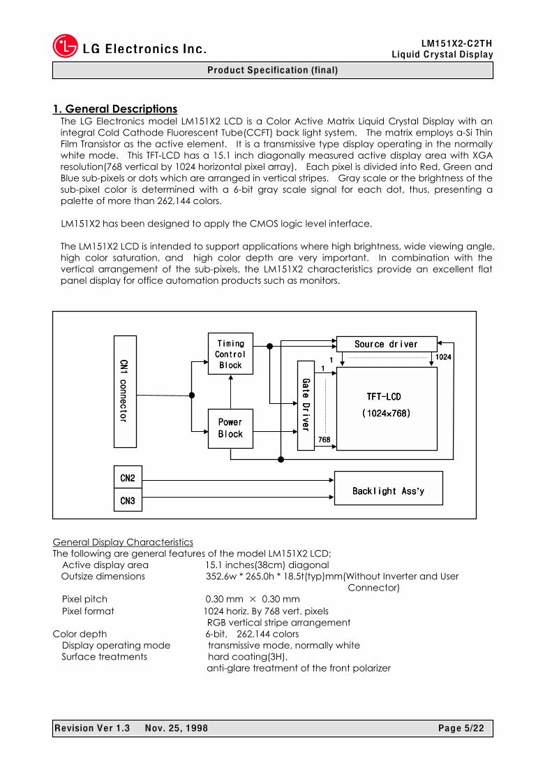
1. General Descriptions
The LG Electronics model LM151X2 LCD is a Color Active Matrix Liquid Crystal Display with an integral Cold Cathode Fluorescent Tube(CCFT) back light system. The matrix employs a-Si Thin Film Transistor as the active element. It is a transmissive type display operating in the normally white mode. This TFT-LCD has a 15.1 inch diagonally measured active display area with XGA resolution(768 vertical by 1024 horizontal pixel array). Each pixel is divided into Red, Green and Blue sub-pixels or dots which are arranged in vertical stripes. Gray scale or the brightness of the sub-pixel color is determined with a 6-bit gray scale signal for each dot, thus, presenting a palette of more than 262,144 colors.
LM151X2 has been designed to apply the CMOS logic level interface. The LM151X2 LCD is intended to support applications where high brightness, wide viewing angle, high color saturation, and high color depth are very important. In combination with the vertical arrangement of the sub-pixels, the LM151X2 characteristics provide an excellent flat panel display for office automation products such as monitors.
General Display Characteristics The following are general features of the model LM151X2 LCD; Active display area 15.1 inches(38cm) diagonal
Outsize dimensions 352.6w * 265.0h * 18.5t(typ)mm(Without Inverter and User Connector)
Pixel pitch 0.30 mm × 0.30 mm Pixel format 1024 horiz. By 768 vert. pixels RGB vertical stripe arrangement Color depth 6-bit, 262,144 colors Display operating mode transmissive mode, normally white
Surface treatments hard coating(3H), anti-glare treatment of the front polarizer
Source driver Source driver Source driver Source driver
Gate Driver
Gate Driver
Gate Driver
Gate Driver
TFT TFT TFT TFT----LCDLCDLCDLCD
(1024 (1024 (1024 (1024××××768)768)768)768)
Timing Timing Timing Timing
Control Control Control Control
BlockBlockBlockBlock
Power Power Power Power
BlockBlockBlockBlock
Backlight AssBacklight AssBacklight AssBacklight Ass’yyyy
CN1 connector
CN1 connector
CN1 connector
CN1 connector
CN2CN2CN2CN2
CN3CN3CN3CN3
1024 1024 1024 1024 1 1 1 1
1 1 1 1
768 768 768 768
R evision V e r 1.3 Nov. 25, 1998 P a g e 6/22
L G E le ctronics Inc. LM151X2- C 2T H Liq uid C rystal Disp lay
Prod u ct Sp e cific ation (final)
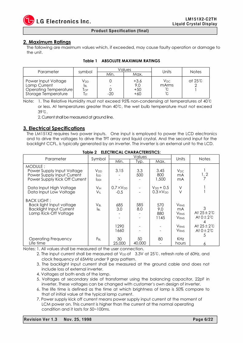
2. Maximum Ratings The following are maximum values which, if exceeded, may cause faulty operation or damage to the unit.
Table 1 ABSOLUTE MAXIMUM RATINGS
Values Parameter symbol Min. Max. Units Notes
Power Input Voltage Lamp Current Operating Temperature Storage Temperature
VDD IBL TOP TST
0 - 0
-20
+3.6 9.0 +50 +60
VDC mArms ℃ ℃
at 25℃ 2 1
Note: 1. The Relative Humidity must not exceed 95% non-condensing at temperatures of 40℃ or less. At temperatures greater than 40℃, the wet bulb temperature must not exceed 39℃. 2. Current shall be measured at ground line.
3. Electrical Specifications
The LM151X2 requires two power inputs. One input is employed to power the LCD electronics and to drive the voltages to drive the TFT array and liquid crystal. And the second input for the backlight CCFL, is typically generated by an inverter. The inverter is an external unit to the LCD.
Table 2 ELECTRICAL CHARACTERISTICS: Values Parameter Symbol Min. Typ. Max. Units Notes
MODULE : Power Supply Input Voltage Power Supply Input Current Power Supply Kick Off Current Data Input High Voltage Data Input Low Voltage
BACK LIGHT : Back light Input voltage Backlight Input Current Lamp Kick-Off Voltage Operating Frequency Life time
VDD IDD IDDI
VIH VIL
VBL IBL
FBL
3.15
- -
0.7×VDD -0.5
685 3.0 - -
1290 1660
30
25,000
3.3 500
- - -
585 8. 0 - - - -
50 40,000
3.45 800
1,500
VDD + 0.5 0.3×VDD
570 9.0 880
1145 - -
80 -
VDC mA mA
V V
VRMS mA VRMS VRMS
VRMS VRMS
KHz
hours
1
1, 2 7
1 1
3 At 25±2℃ At 0±2℃
4 At 25±2℃ At 0±2℃
5
6 Notes: 1. All values shall be measured at the user connection.
2. The input current shall be measured at VDD of 3.3V at 25℃, refresh rate of 60Hz, and clock frequency of 65MHz under 9 gray pattern.
3. The backlight input current shall be measured at the ground cable and does not include loss of external inverter.
4. Voltages at both ends of the lamp. 5. Voltages at secondary side of transformer using the balancing capacitor, 22pF in
inverter. These voltages can be changed with customer’s own design of inverter. 6. The life time is defined as the time at which brightness of lamp is 50% compare to
that of initial value at the typical lamp current. 7. Power supply kick off current means power supply input current at the moment of
LCM power on. This current is higher than the current at the normal operating condition and it lasts for 50~100ms.
R evision V e r 1.3 Nov. 25, 1998 P a g e 7/22
L G E le ctronics Inc. LM151X2- C 2T H Liq uid C rystal Disp lay
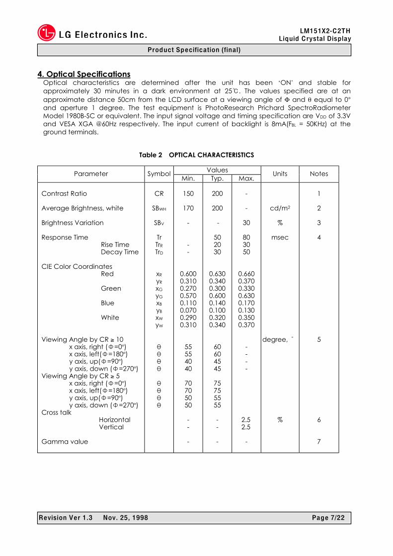
Prod u ct Sp e cific ation (final) 4. Optical Specifications
Optical characteristics are determined after the unit has been ‘ON’ and stable for approximately 30 minutes in a dark environment at 25℃. The values specified are at an approximate distance 50cm from the LCD surface at a viewing angle of Φ and θ equal to 0° and aperture 1 degree. The test equipment is PhotoResearch Prichard SpectroRadiometer Model 1980B-SC or equivalent. The input signal voltage and timing specification are VDD of 3.3V and VESA XGA @60Hz respectively. The input current of backlight is 8mA(FBL = 50KHz) at the ground terminals.
Table 2 OPTICAL CHARACTERISTICS
Values Parameter Symbol Min. Typ. Max.
Units Notes
Contrast Ratio Average Brightness, white Brightness Variation Response Time
Rise Time Decay Time
CIE Color Coordinates
Red Green Blue White
Viewing Angle by CR ≥ 10
x axis, right (Φ=0º) x axis, left(Φ=180º) y axis, up(Φ=90º) y axis, down (Φ=270º)
Viewing Angle by CR ≥ 5 x axis, right (Φ=0º) x axis, left(Φ=180º) y axis, up(Φ=90º) y axis, down (Φ=270º)
Cross talk Horizontal Vertical
Gamma value
CR
SBWH
SBV
Tr TrR TrD
xR yR xG yG xB yB xW yW
θ θ θ θ θ θ θ θ
150
170
- - -
0.600 0.310 0.270 0.570 0.110 0.070 0.290 0.310
55 55 40 40
70 70 50 50
- - -
200
200
-
50 20 30
0.630 0.340 0.300 0.600 0.140 0.100 0.320 0.340
60 60 45 45
75 75 55 55
- - -
- -
30
80 30 50
0.660 0.370 0.330 0.630 0.170 0.130 0.350 0.370
- - - -
2.5 2.5
-
cd/m2
%
msec
degree, °
%
1
2
3
4
5
6
7
R evision V e r 1.3 Nov. 25, 1998 P a g e 8/22
L G E le ctronics Inc. LM151X2- C 2T H Liq uid C rystal Disp lay
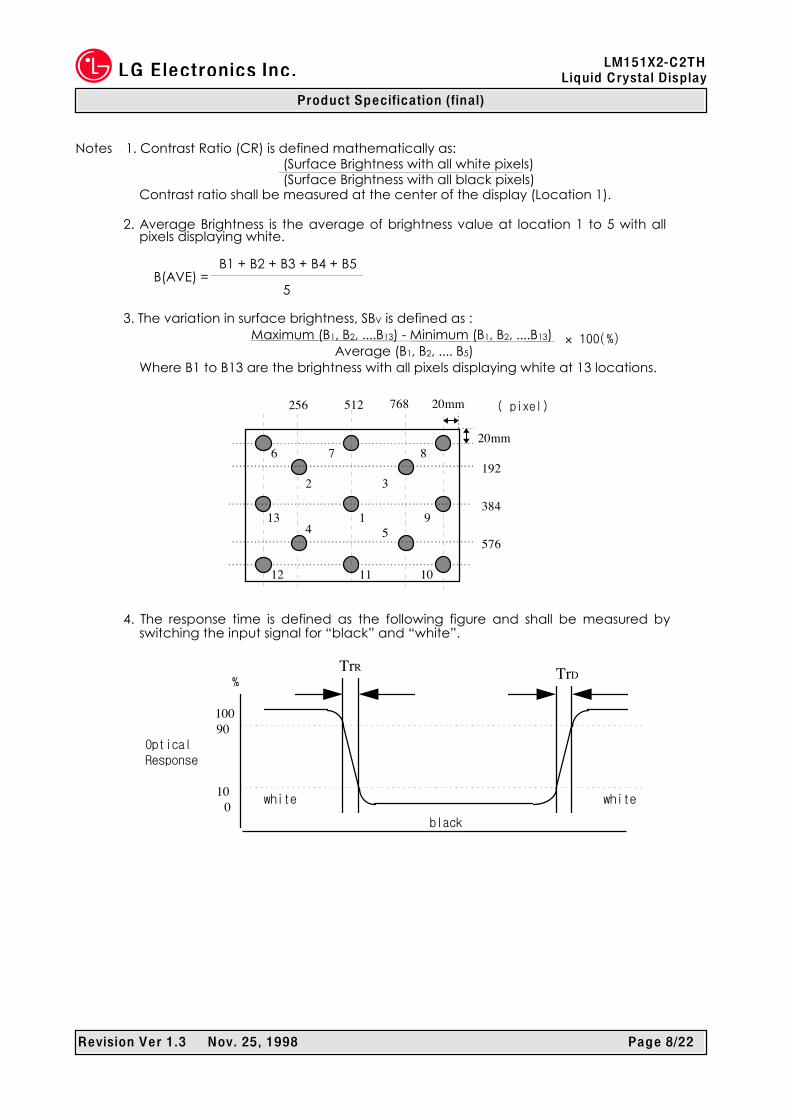
Prod u ct Sp e cific ation (final) Notes 1. Contrast Ratio (CR) is defined mathematically as:
(Surface Brightness with all white pixels) (Surface Brightness with all black pixels)
Contrast ratio shall be measured at the center of the display (Location 1).
2. Average Brightness is the average of brightness value at location 1 to 5 with all pixels displaying white.
B1 + B2 + B3 + B4 + B5 B(AVE) =
5
3. The variation in surface brightness, SBV is defined as : Maximum (B1, B2, ....B13) - Minimum (B1, B2, ....B13)
Average (B1, B2, .... B5) Where B1 to B13 are the brightness with all pixels displaying white at 13 locations.
256 512 20mm
20mm
192
384
576
( pixel)
54
3
13
12 11 10
9
876
2
1
768
4. The response time is defined as the following figure and shall be measured by switching the input signal for “black” and “white”.
TrR TrD
10090
100
%
OpticalResponse
white
black
white
× 100(%)
R evision V e r 1.3 Nov. 25, 1998 P a g e 9/22
L G E le ctronics Inc. LM151X2- C 2T H Liq uid C rystal Disp lay
Prod u ct Sp e cific ation (final)
1 1
2 2
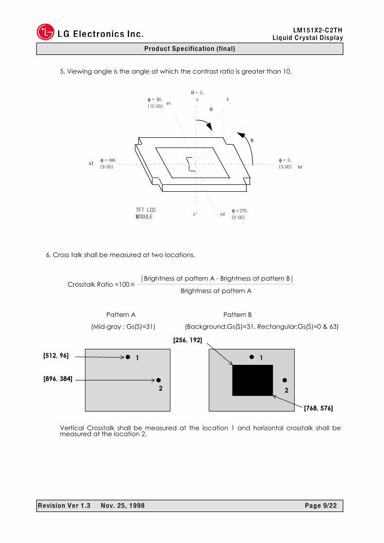
5. Viewing angle is the angle at which the contrast ratio is greater than 10.
φ = 90。(12:00)
yu
θ = 0。z
z' yd
θ
φ
φ = 180。(9:00)
A
φ = 0。(3:00) xr
φ = 270。(6:00)
TFT LCDMODULE
xl
6. Cross talk shall be measured at two locations.
Brightness at pattern A - Brightness at pattern B Crosstalk Ratio =100×
Brightness at pattern A
Pattern A Pattern B
(Mid-gray : Gs(S)=31) (Background:Gs(S)=31, Rectangular:Gs(S)=0 & 63)
Vertical Crosstalk shall be measured at the location 1 and horizontal crosstalk shall be measured at the location 2.
[256, 192]
[512, 96]
[896, 384]
[768, 576]
R evision V e r 1.3 Nov. 25, 1998 P a g e 10/22
L G E le ctronics Inc. LM151X2- C 2T H Liq uid C rystal Disp lay
Prod u ct Sp e cific ation (final)
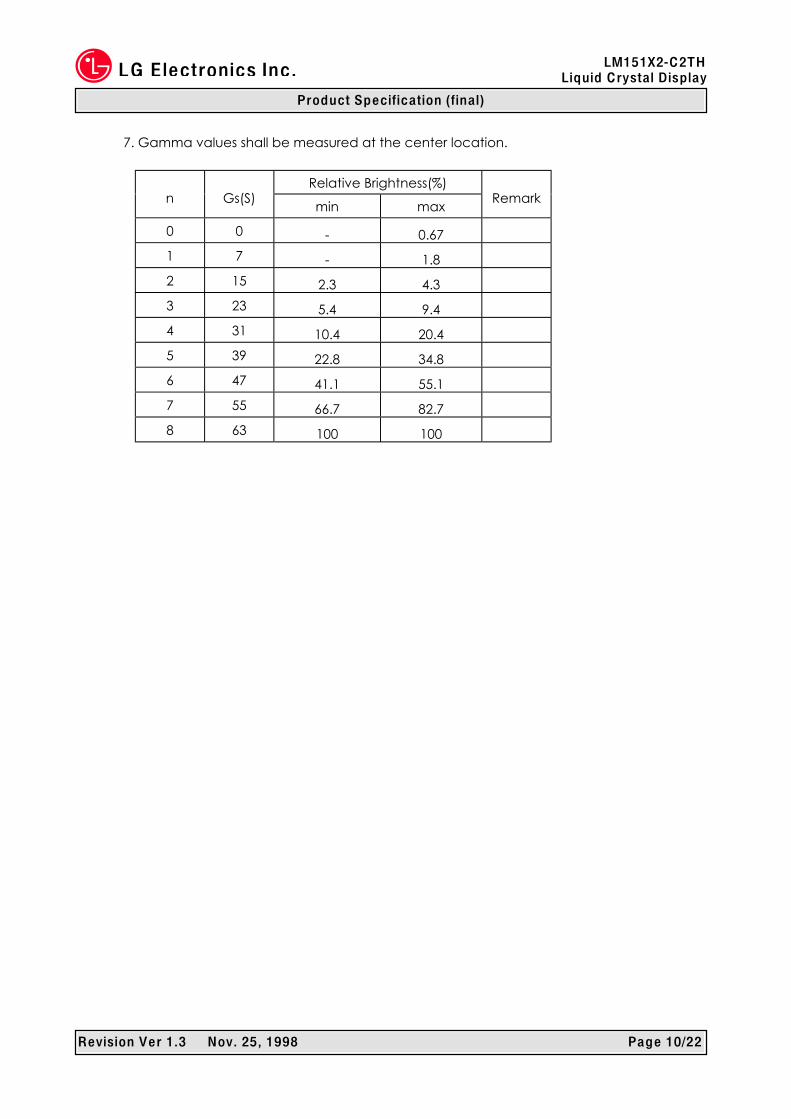
7. Gamma values shall be measured at the center location.
Relative Brightness(%) n Gs(S) min max Remark
0 0 - 0.67
1 7 - 1.8
2 15 2.3 4.3
3 23 5.4 9.4
4 31 10.4 20.4
5 39 22.8 34.8
6 47 41.1 55.1
7 55 66.7 82.7
8 63 100 100
R evision V e r 1.3 Nov. 25, 1998 P a g e 11/22
L G E le ctronics Inc. LM151X2- C 2T H Liq uid C rystal Disp lay
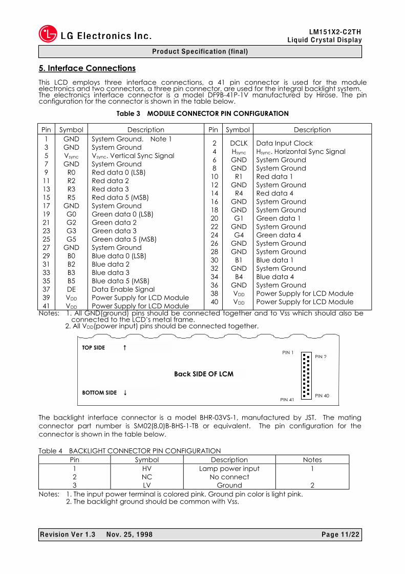
Prod u ct Sp e cific ation (final) 5. Interface Connections This LCD employs three interface connections, a 41 pin connector is used for the module electronics and two connectors, a three pin connector, are used for the integral backlight system. The electronics interface connector is a model DF9B-41P-1V manufactured by Hirose. The pin configuration for the connector is shown in the table below.
Table 3 MODULE CONNECTOR PIN CONFIGURATION
Pin Symbol Description Pin Symbol Description 1 3 5 7 9
11 13 15 17 19 21 23 25 27 29 31 33 35 37 39 41
GND GND Vsync GND
R0 R2 R3 R5
GND G0 G2 G3 G5
GND B0 B2 B3 B5 DE VDD
VDD
System Ground. Note 1 System Ground Vsync. Vertical Sync Signal System Ground Red data 0 (LSB) Red data 2 Red data 3 Red data 5 (MSB) System Ground Green data 0 (LSB) Green data 2 Green data 3 Green data 5 (MSB) System Ground Blue data 0 (LSB) Blue data 2 Blue data 3 Blue data 5 (MSB) Data Enable Signal Power Supply for LCD Module Power Supply for LCD Module
2 4 6 8
10 12 14 16 18 20 22 24 26 28 30 32 34 36 38 40
DCLK Hsync GND GND
R1 GND
R4 GND GND G1
GND G4
GND GND
B1 GND
B4 GND VDD VDD
Data Input Clock Hsync. Horizontal Sync Signal System Ground System Ground Red data 1 System Ground Red data 4 System Ground System Ground Green data 1 System Ground Green data 4 System Ground System Ground Blue data 1 System Ground Blue data 4 System Ground Power Supply for LCD Module Power Supply for LCD Module
Notes: 1. All GND(ground) pins should be connected together and to Vss which should also be connected to the LCD’s metal frame.
2. All VDD(power input) pins should be connected together. The backlight interface connector is a model BHR-03VS-1, manufactured by JST. The mating connector part number is SM02(8.0)B-BHS-1-TB or equivalent. The pin configuration for the connector is shown in the table below. Table 4 BACKLIGHT CONNECTOR PIN CONFIGURATION
Pin Symbol Description Notes 1 2 3
HV NC LV
Lamp power input No connect
Ground
1
2 Notes: 1. The input power terminal is colored pink. Ground pin color is light pink. 2. The backlight ground should be common with Vss.
TOP SIDE ↑↑↑↑
Back SIDE OF LCM
BOTTOM SIDE ↓↓↓↓ PIN 41
PIN 40
PIN 1 PIN 2
R evision V e r 1.3 Nov. 25, 1998 P a g e 12/22
L G E le ctronics Inc. LM151X2- C 2T H Liq uid C rystal Disp lay
Prod u ct Sp e cific ation (final)
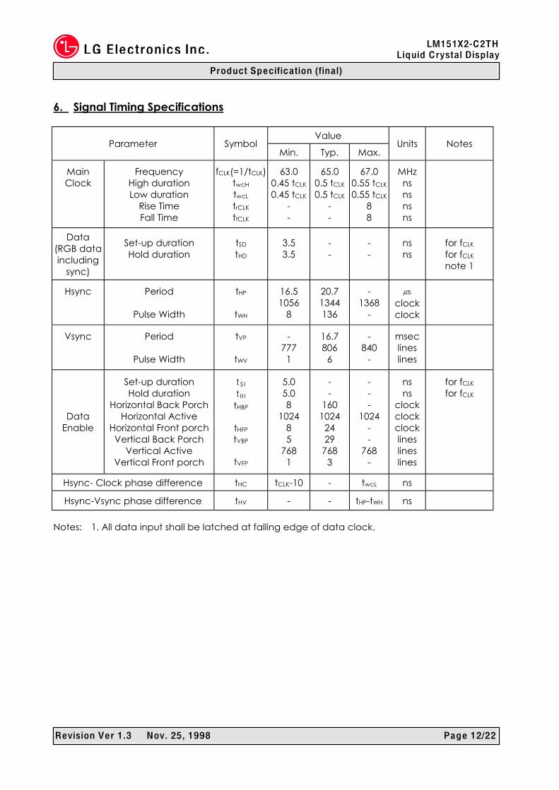
6. Signal Timing Specifications
Value Parameter Symbol
Min. Typ. Max. Units Notes
Main Clock
Frequency High duration Low duration
Rise Time Fall Time
fCLK(=1/tCLK) twcH
twcL
trCLK
tfCLK
63.0 0.45 tCLK 0.45 tCLK
- -
65.0 0.5 tCLK 0.5 tCLK
- -
67.0 0.55 tCLK 0.55 tCLK
8 8
MHz ns ns ns ns
Data (RGB data including
sync)
Set-up duration Hold duration
tSD
tHD
3.5 3.5
- -
- -
ns ns
for fCLK
for fCLK
note 1
Hsync
Period
Pulse Width
tHP
tWH
16.5 1056
8
20.7 1344 136
- 1368
-
㎲ clock clock
Vsync
Period
Pulse Width
tVP
tWV
- 777
1
16.7 806
6
- 840
-
msec lines lines
Data
Enable
Set-up duration Hold duration
Horizontal Back Porch Horizontal Active
Horizontal Front porch Vertical Back Porch
Vertical Active Vertical Front porch
tSI tHI tHBP
tHFP tVBP
tVFP
5.0 5.0 8
1024 8 5
768 1
- -
160 1024
24 29
768 3
- - -
1024 - -
768 -
ns ns
clock clock clock lines lines lines
for fCLK
for fCLK
Hsync- Clock phase difference tHC tCLK-10 - twcL ns
Hsync-Vsync phase difference tHV - - tHP-tWH ns
Notes: 1. All data input shall be latched at falling edge of data clock.
R evision V e r 1.3 Nov. 25, 1998 P a g e 13/22
L G E le ctronics Inc. LM151X2- C 2T H Liq uid C rystal Disp lay
Prod u ct Sp e cific ation (final)
7. Signal Timimg Waveforms
Invalid Data Invalid Data Invalid Data Invalid Data Invalid Data Invalid Data Invalid Data Invalid Data
0.7VDD
0.7VDD
0.7VDD 0.7VDD 0.5VDD 0.5VDD 0.5VDD
0.3VDD 0.3VDD 0.3VDD 0.3VDD
MainMainMainMain
ClockClockClockClock
DataDataDataData (R0~R5,(R0~R5,(R0~R5,(R0~R5,
G0~G5,G0~G5,G0~G5,G0~G5,
B0~B5)B0~B5)B0~B5)B0~B5)
DataDataDataData----
EnableEnableEnableEnable
HsyncHsyncHsyncHsync
VsyncVsyncVsyncVsync
HsyncHsyncHsyncHsync
DataDataDataData----
EnableEnableEnableEnable
VsyncVsyncVsyncVsync
DataDataDataData----
EnableEnableEnableEnable
tCLK tWCH tWCL tfCLK trCLK
tHD tSD
tHI tSI
tHV
tWH
tHP
tHFP tHBP
tVP
tWV
tVBP tVFP
MainMainMainMain
ClockClockClockClock
tHC
R evision V e r 1.3 Nov. 25, 1998 P a g e 14/22
L G E le ctronics Inc. LM151X2- C 2T H Liq uid C rystal Disp lay
Prod u ct Sp e cific ation (final)
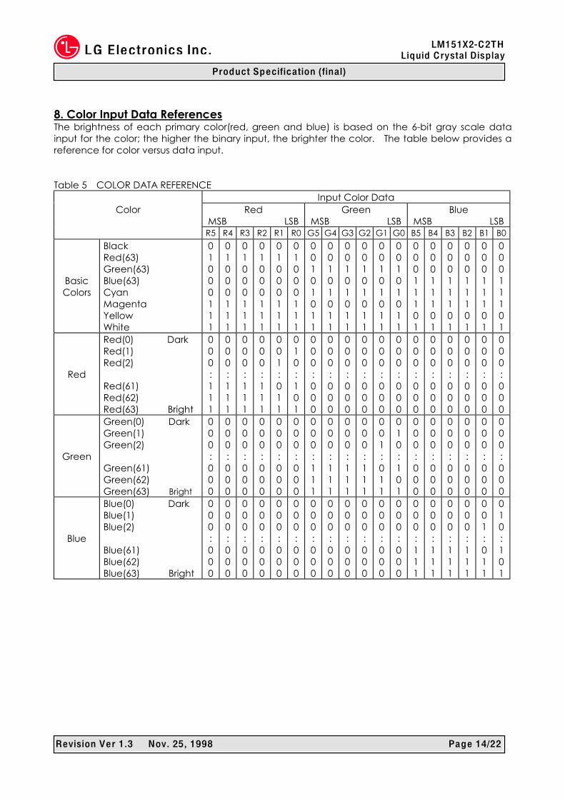
8. Color Input Data References The brightness of each primary color(red, green and blue) is based on the 6-bit gray scale data input for the color; the higher the binary input, the brighter the color. The table below provides a reference for color versus data input. Table 5 COLOR DATA REFERENCE
Input Color Data Color Red
MSB LSB Green
MSB LSB Blue
MSB LSB R5 R4 R3 R2 R1 R0 G5 G4 G3 G2 G1 G0 B5 B4 B3 B2 B1 B0
Basic Colors
Black Red(63) Green(63) Blue(63) Cyan Magenta Yellow White
0 1 0 0 0 1 1 1
0 1 0 0 0 1 1 1
0 1 0 0 0 1 1 1
0 1 0 0 0 1 1 1
0 1 0 0 0 1 1 1
0 1 0 0 0 1 1 1
0 0 1 0 1 0 1 1
0 0 1 0 1 0 1 1
0 0 1 0 1 0 1 1
0 0 1 0 1 0 1 1
0 0 1 0 1 0 1 1
0 0 1 0 1 0 1 1
0 0 0 1 1 1 0 1
0 0 0 1 1 1 0 1
0 0 0 1 1 1 0 1
0 0 0 1 1 1 0 1
0 0 0 1 1 1 0 1
0 0 0 1 1 1 0 1
Red
Red(0) Dark Red(1) Red(2) Red(61) Red(62) Red(63) Bright
0 0 0 : 1 1 1
0 0 0 : 1 1 1
0 0 0 : 1 1 1
0 0 0 : 1 1 1
0 0 1 : 0 1 1
0 1 0 : 1 0 1
0 0 0 : 0 0 0
0 0 0 : 0 0 0
0 0 0 : 0 0 0
0 0 0 : 0 0 0
0 0 0 : 0 0 0
0 0 0 : 0 0 0
0 0 0 : 0 0 0
0 0 0 : 0 0 0
0 0 0 : 0 0 0
0 0 0 : 0 0 0
0 0 0 : 0 0 0
0 0 0 : 0 0 0
Green
Green(0) Dark Green(1) Green(2) Green(61) Green(62) Green(63) Bright
0 0 0 : 0 0 0
0 0 0 : 0 0 0
0 0 0 : 0 0 0
0 0 0 : 0 0 0
0 0 0 : 0 0 0
0 0 0 : 0 0 0
0 0 0 : 1 1 1
0 0 0 : 1 1 1
0 0 0 : 1 1 1
0 0 0 : 1 1 1
0 0 1 : 0 1 1
0 1 0 : 1 0 1
0 0 0 : 0 0 0
0 0 0 : 0 0 0
0 0 0 : 0 0 0
0 0 0 : 0 0 0
0 0 0 : 0 0 0
0 0 0 : 0 0 0
Blue
Blue(0) Dark Blue(1) Blue(2) Blue(61) Blue(62) Blue(63) Bright
0 0 0 : 0 0 0
0 0 0 : 0 0 0
0 0 0 : 0 0 0
0 0 0 : 0 0 0
0 0 0 : 0 0 0
0 0 0 : 0 0 0
0 0 0 : 0 0 0
0 0 0 : 0 0 0
0 0 0 : 0 0 0
0 0 0 : 0 0 0
0 0 0 : 0 0 0
0 0 0 : 0 0 0
0 0 0 : 1 1 1
0 0 0 : 1 1 1
0 0 0 : 1 1 1
0 0 0 : 1 1 1
0 0 1 : 0 1 1
0 1 0 : 1 0 1
R evision V e r 1.3 Nov. 25, 1998 P a g e 15/22
L G E le ctronics Inc. LM151X2- C 2T H Liq uid C rystal Disp lay
Prod u ct Sp e cific ation (final)
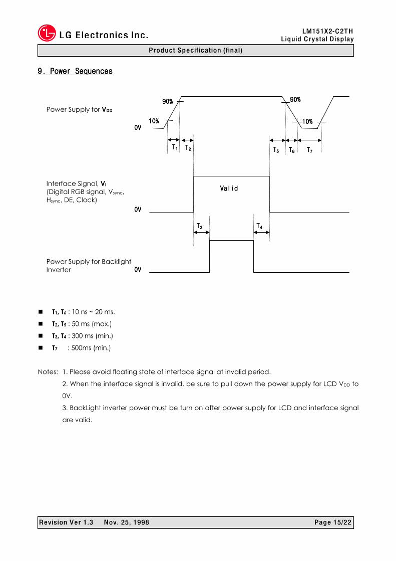
TTTT7777 TTTT6666
9. Power Sequences9. Power Sequences9. Power Sequences9. Power Sequences
! T1, T6 : 10 ns ~ 20 ms.
! T2, T5 : 50 ms (max.)
! T3, T4 : 300 ms (min.)
! T7 : 500ms (min.)
Notes: 1. Please avoid floating state of interface signal at invalid period.
2. When the interface signal is invalid, be sure to pull down the power supply for LCD VDD to
0V.
3. BackLight inverter power must be turn on after power supply for LCD and interface signal
are valid.
Interface Signal, Vi (Digital RGB signal, Vsync, Hsync, DE, Clock)
Power Supply for Backlight Inverter
Power Supply for VDD 90%90%90%90%
10%10%10%10% 10%10%10%10% 0V0V0V0V
90%90%90%90%
TTTT1111 TTTT2222 TTTT5555
Valid Valid Valid Valid
0V0V0V0V
0V0V0V0V
TTTT3333 TTTT4444
R evision V e r 1.3 Nov. 25, 1998 P a g e 16/22
L G E le ctronics Inc. LM151X2- C 2T H Liq uid C rystal Disp lay
Prod u ct Sp e cific ation (final)
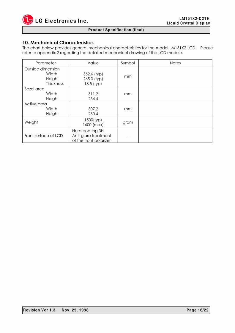
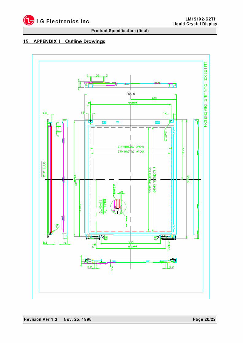
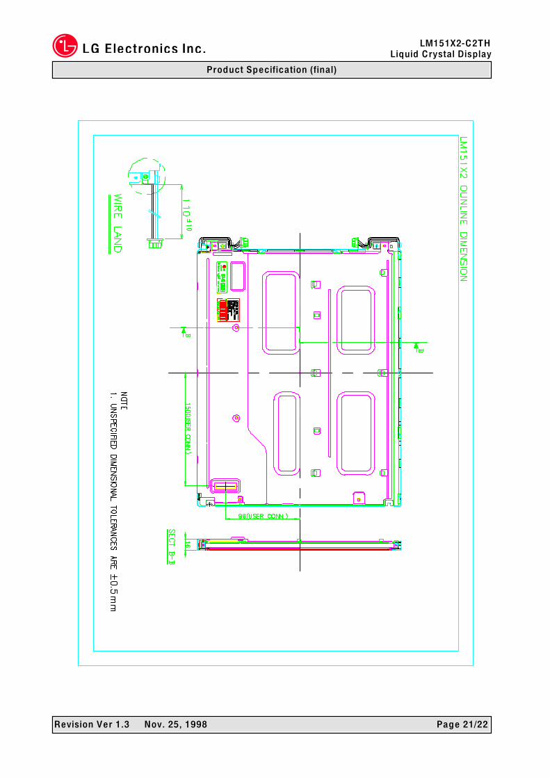
10. Mechanical Characteristics The chart below provides general mechanical characteristics for the model LM151X2 LCD. Please refer to appendix 2 regarding the detailed mechanical drawing of the LCD module.
Parameter Value Symbol Notes Outside dimension
Width Height Thickness
352.6 (typ) 265.0 (typ) 18.5 (typ)
mm
Bezel area Width Height
311.2 234.4
mm
Active area Width Height
307.2 230.4
mm
Weight 1500(typ) 1600 (max) gram
Front surface of LCD Hard coating 3H. Anti-glare treatment of the front polarizer
-
R evision V e r 1.3 Nov. 25, 1998 P a g e 17/22
L G E le ctronics Inc. LM151X2- C 2T H Liq uid C rystal Disp lay
Prod u ct Sp e cific ation (final)
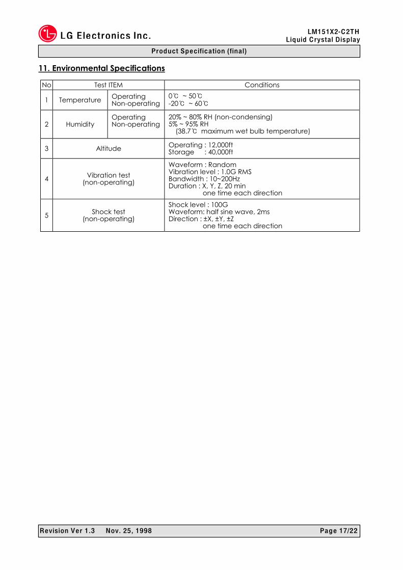
11. Environmental Specifications
No Test ITEM Conditions
1 Temperature Operating Non-operating
0℃ ~ 50℃ -20℃ ~ 60℃
2 Humidity Operating Non-operating
20% ~ 80% RH (non-condensing) 5% ~ 95% RH (38.7℃ maximum wet bulb temperature)
3 Altitude Operating : 12,000ft Storage : 40,000ft
4 Vibration test (non-operating)
Waveform : Random Vibration level : 1.0G RMS Bandwidth : 10~200Hz Duration : X, Y, Z, 20 min one time each direction
5 Shock test (non-operating)
Shock level : 100G
Waveform: half sine wave, 2ms Direction : ±X, ±Y, ±Z one time each direction
R evision V e r 1.3 Nov. 25, 1998 P a g e 18/22
L G E le ctronics Inc. LM151X2- C 2T H Liq uid C rystal Disp lay
Prod u ct Sp e cific ation (final)
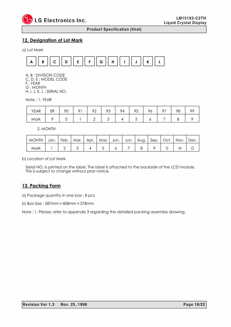
12. Designation of Lot Mark a) Lot Mark
A, B : DIVISION CODE C, D, E : MODEL CODE F : YEAR G : MONTH H, I, J, K, L : SERIAL NO. Note : 1. YEAR
YEAR 89 90 91 92 93 94 95 96 97 98 99
Mark 9 0 1 2 3 4 5 6 7 8 9
2. MONTH
MONTH Jan. Feb. Mar. Apr. May Jun. Jun. Aug. Sep. Oct. Nov. Dec.
Mark 1 2 3 4 5 6 7 8 9 0 N D b) Location of Lot Mark
Serial NO. Is printed on the label. The label is attached to the backside of the LCD module. This is subject to change without prior notice.
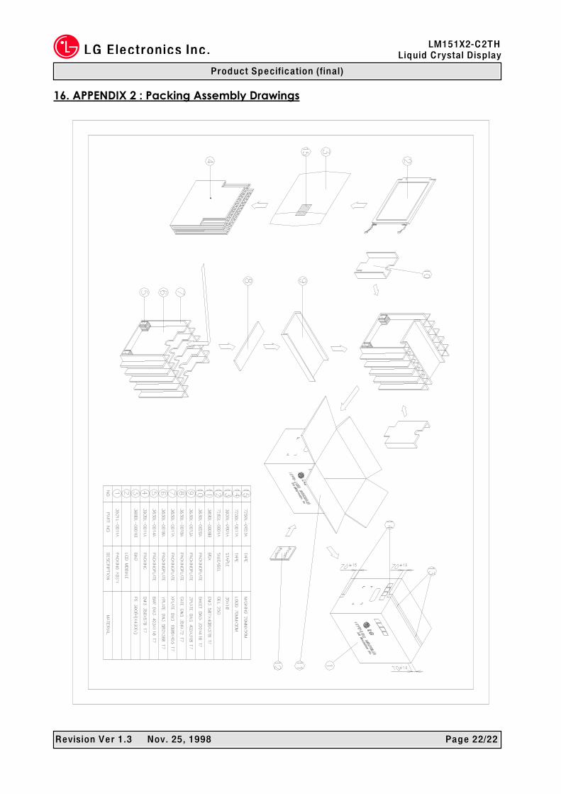
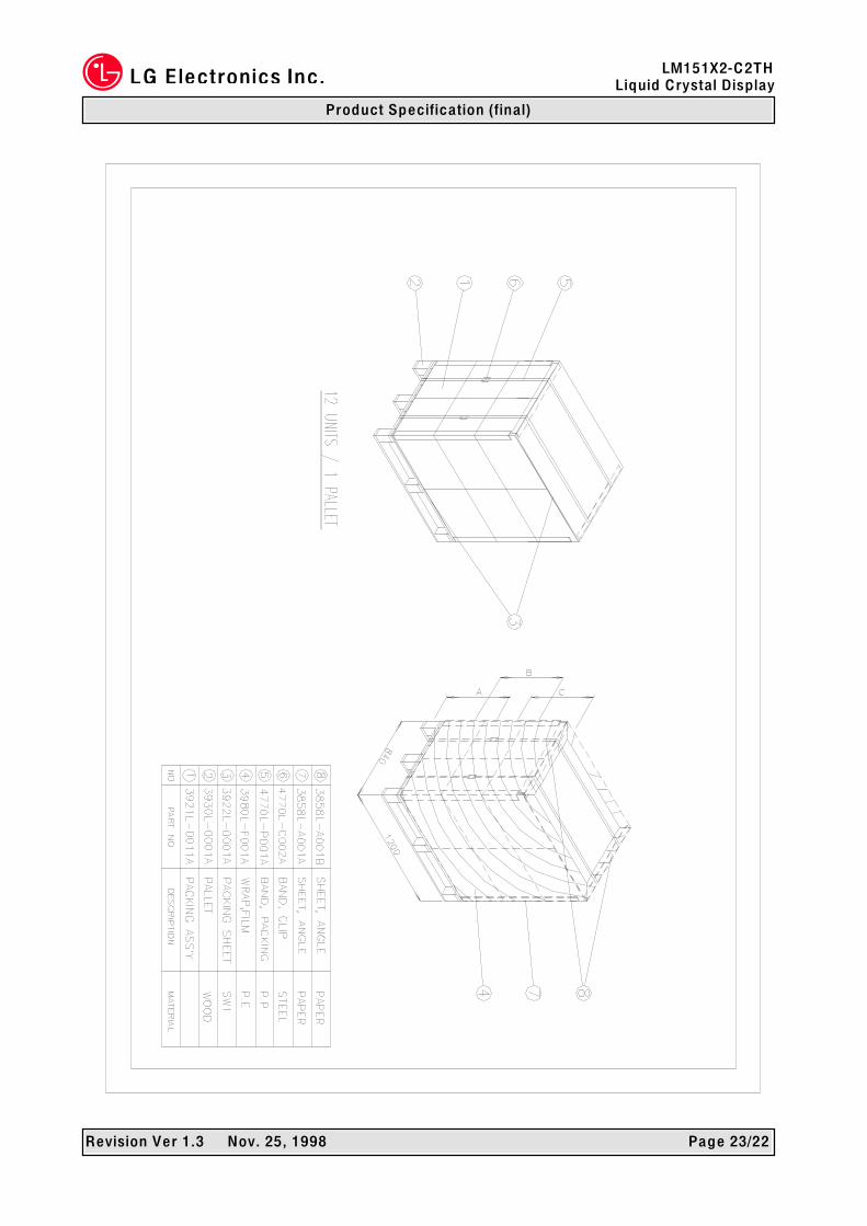
13. Packing Form a) Package quantity in one box : 8 pcs b) Box Size : 587mm×408mm×378mm Note : 1. Please, refer to appendix 3 regarding the detailed packing assembly drawing.
K J I H G F E D C B A L
R evision V e r 1.3 Nov. 25, 1998 P a g e 19/22
L G E le ctronics Inc. LM151X2- C 2T H Liq uid C rystal Disp lay
Prod u ct Sp e cific ation (final)
14. PRECAUTIONS Please pay attention to the followings when you use this TFT-LCD module with Back-light unit.
1)You must mount Module using mounting holes arranged in 4 corners. 2) Be sure to turn off the power when connecting or disconnecting the circuit. 3) Note that the polarizers are easily damaged. Pay attention not to scratch or press this
surface with any hard object.
4) When the LCD surface become dirty, please wipe it off with a soft material. (ie. cotton ball) 5) Protect the module from the ESD as it may damage the electronic circuit (C-MOS).
Make certain that treatment person’s body are grounded through wrist bend.
6) Do not disassemble the module and be careful not to incur a mechanical shock that might occur during installation. It may cause permanent damage.
7) Do not leave the module in high temperatures, particularly in areas of high humidity for a long time. 8) The module not be expose to the direct sunlight. 9) Avoid contact with water as it may a short circuit within the module.
10) Do not apply invalid signal, especially very high frequency data clock and Hsync. Invalid signal causes improper shutdown of DC/DC converter in LCM or permanent damage to LCD module. (If DC/DC converter in LCM is in shutdown state, LCM shows only white screen. Then please turn off and on once LCM power.) 11) If the LCM displays the same pattern continuously for a long period of time, it can be the image sticking to the screen.
R evision V e r 1.3 Nov. 25, 1998 P a g e 20/22
L G E le ctronics Inc. LM151X2- C 2T H Liq uid C rystal Disp lay
Prod u ct Sp e cific ation (final)
15. 15. 15. 15. APPENDIX 1 : Outline Drawings
265.0
R evision V e r 1.3 Nov. 25, 1998 P a g e 21/22
L G E le ctronics Inc. LM151X2- C 2T H Liq uid C rystal Disp lay
Prod u ct Sp e cific ation (final)
R evision V e r 1.3 Nov. 25, 1998 P a g e 22/22
L G E le ctronics Inc. LM151X2- C 2T H Liq uid C rystal Disp lay
Prod u ct Sp e cific ation (final) 16. APPENDIX 2 : Packing Assembly Drawings
R evision V e r 1.3 Nov. 25, 1998 P a g e 23/22
L G E le ctronics Inc. LM151X2- C 2T H Liq uid C rystal Disp lay
Prod u ct Sp e cific ation (final)
Recommended