IC Packaging
By,SANTOSH NIMBAL
Contents● Objective
● Package Overview
● Through-Hole package
● Surface mount package
● Chip-Scale Package (CSP)
○ Wire Bonded BGA○ FC-BGA
● Wafer Level Chip-Scale Package (WL-CSP)
● Advantages of WL-CSP
IC PACKAGING

Objective● To discuss and understand the various packaging
technologies.
○ WCSP package○ PBGA package etc
● Learn advantages and disadvantages of different packaging types.
IC PACKAGING

Package Overview● Development of IC package is a Dynamic technology.
● From mobile telecommunication and satellite broadcasting to aerospace and automotive applications each imposes its own demands on electronic package.
● To meet such diverse range of requirements, IC package range encompasses over 30 different types.
● An overview of this range is shown in fig. 1
IC PACKAGING

IC PACKAGING
Package Overview
Fig. 1 :Package classification
IC PACKAGING

Through-Hole mount Package
Fig. 2 :Through-Hole Packages
IC PACKAGING

Through-Hole mount Package● Refers to the mounting scheme that involves the use of
leads on the components that are inserted into holes (PTH - Plated Through-Hole) drilled in printed circuit boards (PCB) and soldered to pads on the opposite side.
● Provides strong mechanical bonds when compared to surface-mount techniques, the additional drilling required makes the boards more expensive to produce.
● These techniques are now usually reserved for bulkier components such as electrolytic capacitors, that require the additional mounting strength.
IC PACKAGING
IC PACKAGING
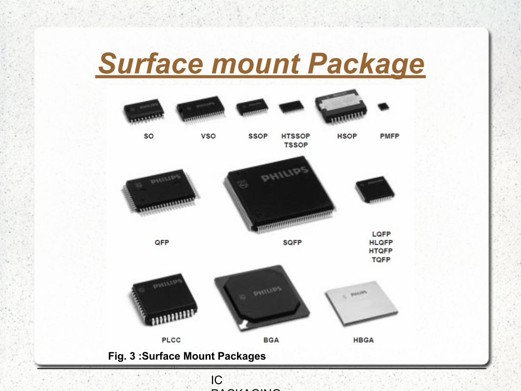
Surface mount Package
Fig. 3 :Surface Mount Packages
IC PACKAGING

Surface mount Package● In SMT the components are mounted directly onto the
surface of printed circuit boards.
● It has largely replaced the through-hole technology.
● SMT component is usually smaller than its through-hole counterpart because it has either smaller leads or no leads at all. It may have short pins or leads of various styles, flat contacts, a matrix of solder balls (BGAs).
● Advantages
● Smaller components.
● Fewer holes need to be drilled through abrasive boards.
IC PACKAGING

Surface mount Package● Components can be placed on both sides of the circuit
board.
● Lower resistance and inductance at the connection......
● Disadvantages
● The manufacturing processes for SMT are much more sophisticated than through-hole boards.
● SMDs can't be used directly with breadboards.
● SMDs' solder connections may be damaged by potting compounds going through thermal cycling.
● And so on....
IC PACKAGING

Chip-Scale Package (CSP)● CSP is a type of integrated circuit chip carrier.
● Definition, is a single-die, direct surface mountable package with an area of no more than 1.2 X the original die area..
● Definition likewise doesn't define how a chip scale package is to be constructed, so any package that meets the surface mountability and dimensional requirements of the definition is a CSP, regardless of structure. For this reason, CSP's come in many forms - flip-chip, wire-bonded, ball grid array, leaded, etc.
IC PACKAGING
IC PACKAGING
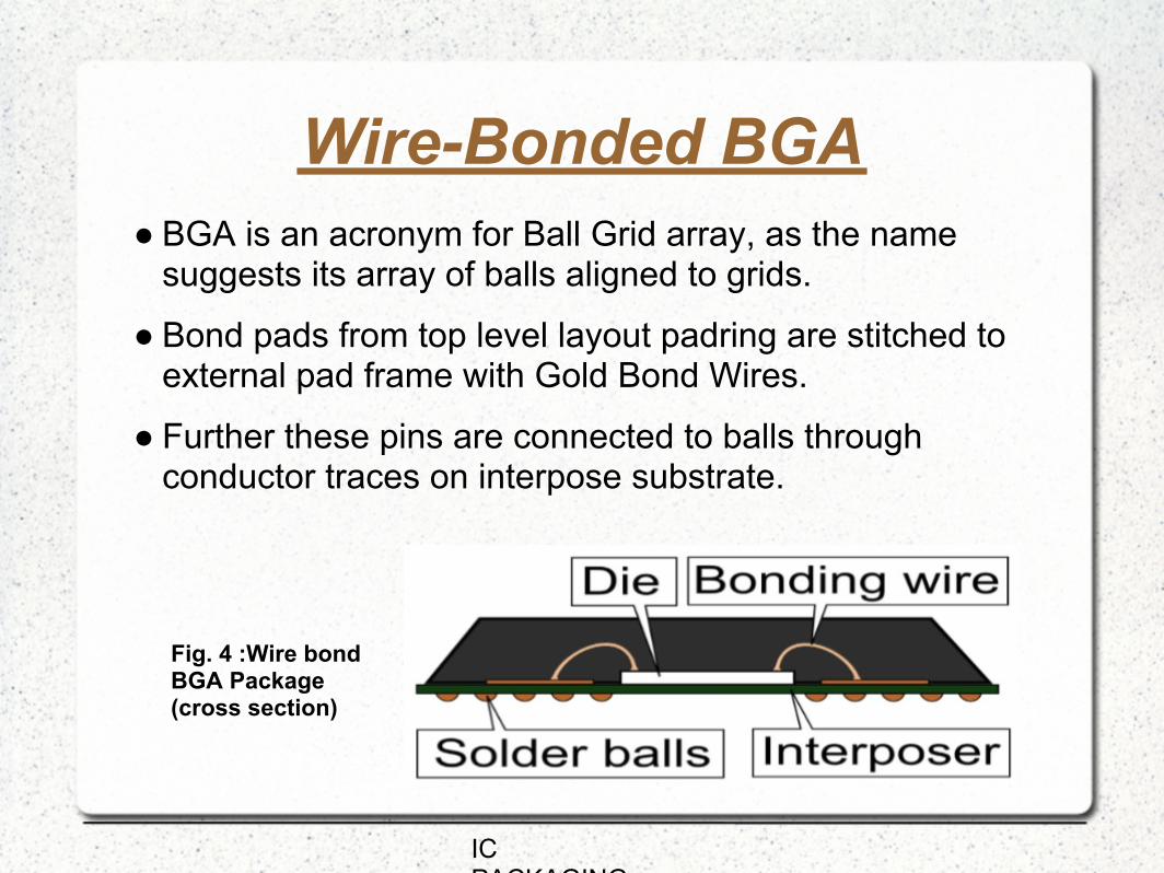
Wire-Bonded BGA● BGA is an acronym for Ball Grid array, as the name
suggests its array of balls aligned to grids.
● Bond pads from top level layout padring are stitched to external pad frame with Gold Bond Wires.
● Further these pins are connected to balls through conductor traces on interpose substrate.
Fig. 4 :Wire bond BGA Package (cross section)
IC PACKAGING

Wire-Bonded BGA
Fig. 5 :Wire bond BGA Package
IC PACKAGING

Flip Chip - BGA● In Flip Chip BGA the chip/die is flipped, bond pads in
padring layout are connected to external ball grid array via conductor traces on layered substrate.
● During packaging solder bumps are formed on bondpads which align and make contact with conductor traces when flipped.
● Flip-chip packaging techniques connect die bond pads to a package substrate without using wirebonds. The bumped die is placed on the package substrate where the bumps connect to the package pins/balls.
IC PACKAGING

Flip Chip - BGA
Fig. 7 :Flip chip BGA construction and Substrate cross section
Fig. 8 :In this gold stud bump, the gold ball has been pressed flat on the bond pad, with the wire stub protruding from the top of the bump.
IC PACKAGING
Flip Chip - BGA● Advantages
● Lower inductance power planes support high frequency designs
● Supports higher pin counts than wirebond packages
● Improved current distribution providing more ability to minimize IR drops (power is distributed through top metal layer metal bumps)
IC PACKAGING

Flip Chip - BGA
Fig. 9 :Difference between Wire Bond CSP and FC
IC PACKAGING

Wafer Level Chip-Scale Package (WL-CSP)
● In this type of technology packaging is done at the Wafer level, and then dicing is performed .
Fig. 10 :Comparison between Conventional CSP and WLCSP
IC PACKAGING

Wafer Level Chip-Scale Package● WLP allows direct connection, without wires, to a printed
circuit board by inverting the die and connecting by solder balls.
● WLP chips are manufactured by building up the package interconnect structure directly on the silicon circuit substrate.
● A dielectric repassivation polymer film is applied over the active wafer surface. This film provides both mechanical stress relief for the ball attachment, and electrical isolation on the die surface.
● Here CSP can be expanded as Chip-SIZE Package.
IC PACKAGING

Wafer Level Chip-Scale Package
IC PACKAGING
Fig. 11 :WLP layers

Wafer Level Chip-Scale Package● Wafer level package is different from FC, as FC requires
the presence of Interposer substrate .
IC PACKAGING
Interposer Substrate
FC-BGA WLCSP
Fig. 12 :Comparison between WLCSP and FC

Wafer Level Chip-Scale Package Evolution of Silicon Wafer in size
Fig. 13 :Evolution of Silicon wafer in size
IC PACKAGING

Wafer Level Chip-Scale Package● Advantages of WLP
● WLP are a small package size, a minimized IC to PCB inductance and shortened manufacture cycle time.
● Lighter weight and thinner package profile due to elimination of lead frame and molding compound.
● No under-fill required. Economical.
● Draw backs : Very high I/O IC’s would require very small solder balls on a very tight pitch. Requires very high density PCB to interconnect-expensive.
● All the IC’s (good and bad) are packaged at the wafer level
IC PACKAGING

Wafer Level Chip-Scale Package
Thank You
IC PACKAGING
Recommended