Optical and
Electron MicroscopyMSN 506
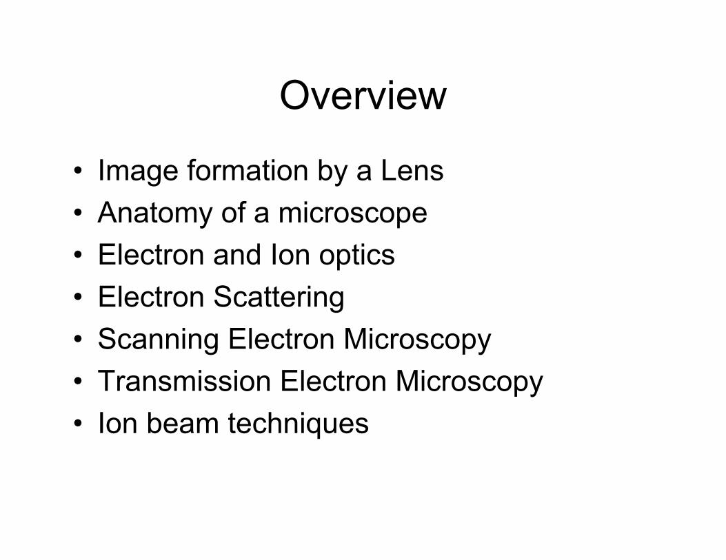
Overview
• Image formation by a Lens• Anatomy of a microscope• Electron and Ion optics• Electron Scattering• Scanning Electron Microscopy• Transmission Electron Microscopy• Ion beam techniques
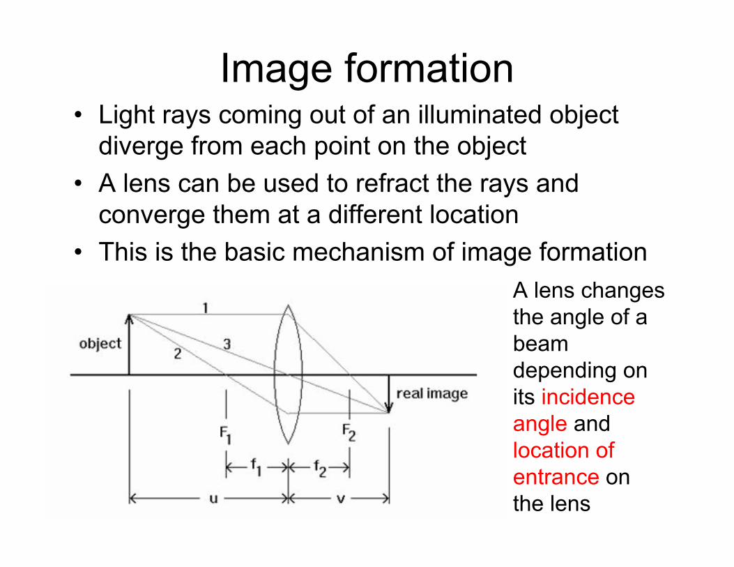
Image formation• Light rays coming out of an illuminated object
diverge from each point on the object• A lens can be used to refract the rays and
converge them at a different location• This is the basic mechanism of image formation
A lens changes the angle of a beam depending on its incidence angle and location of entrance on the lens
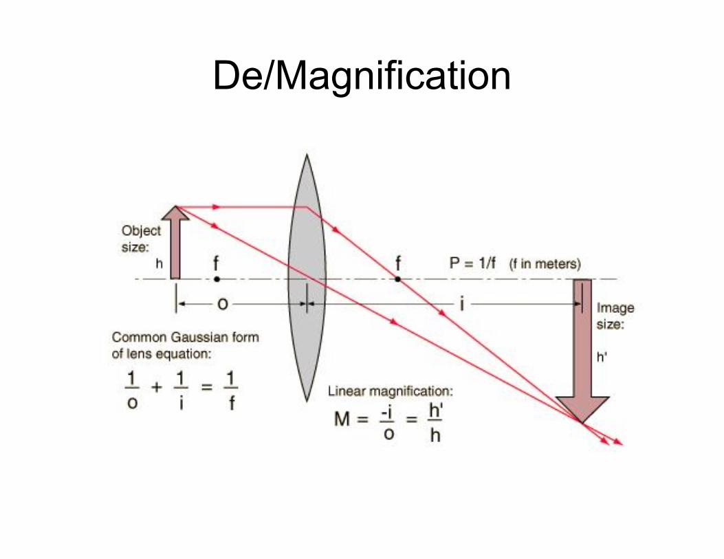
De/Magnification
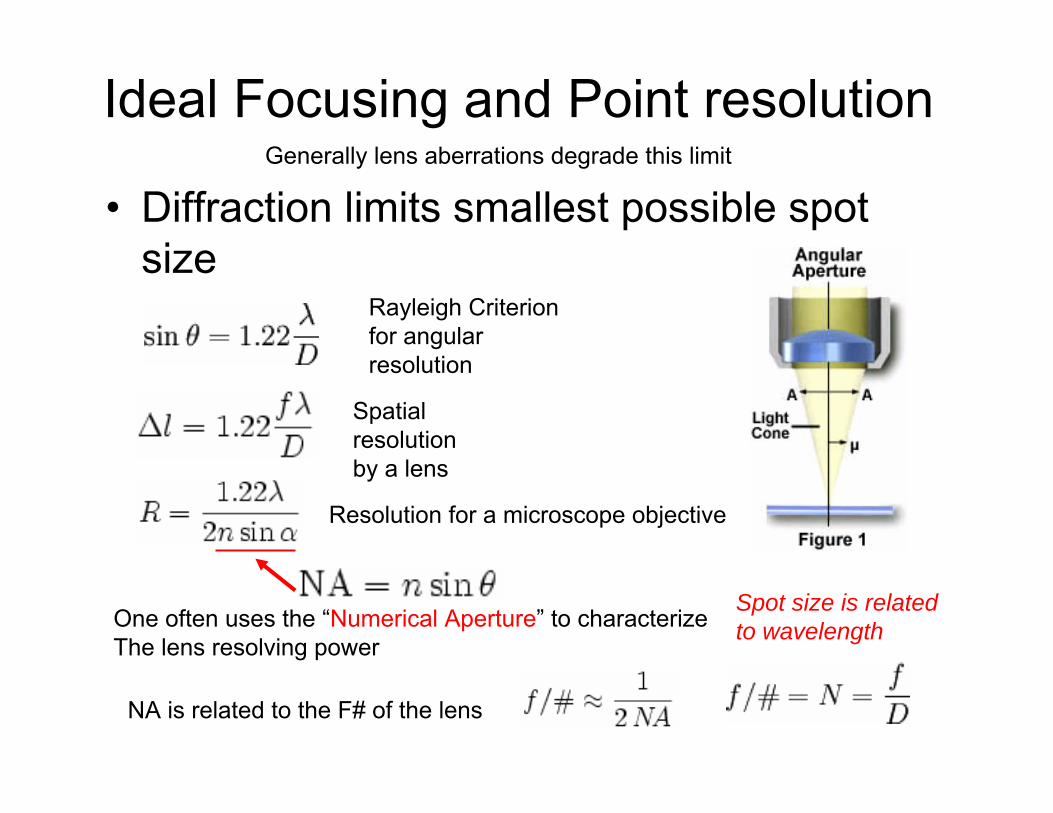
Ideal Focusing and Point resolution
• Diffraction limits smallest possible spot size
Rayleigh Criterion for angular resolution
Spatial resolution by a lens
Resolution for a microscope objective
One often uses the “Numerical Aperture” to characterizeThe lens resolving power
NA is related to the F# of the lens
Spot size is related to wavelength
Generally lens aberrations degrade this limit
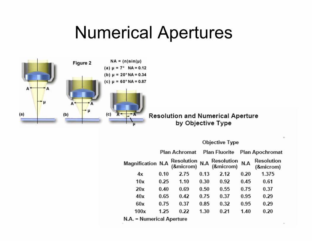
Numerical Apertures
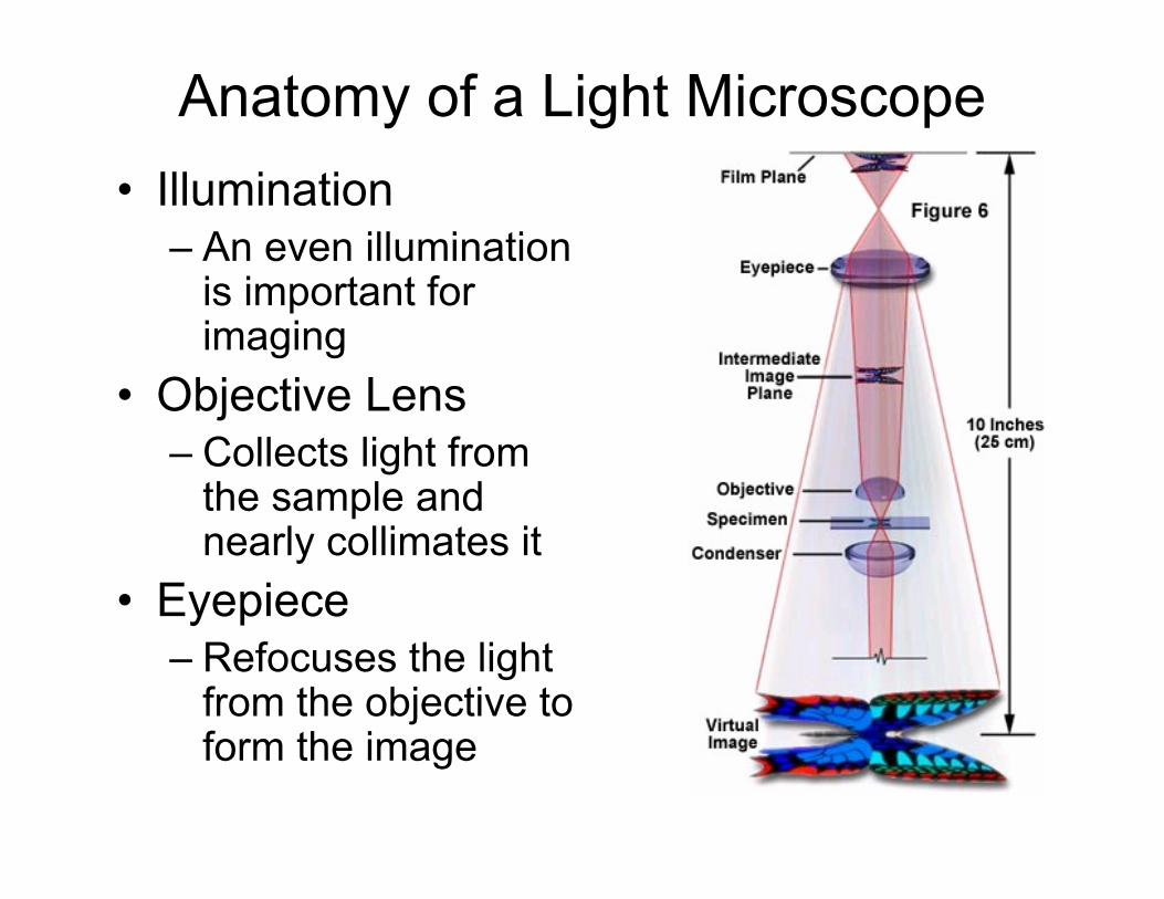
Anatomy of a Light Microscope• Illumination
– An even illumination is important for imaging
• Objective Lens– Collects light from
the sample and nearly collimates it
• Eyepiece– Refocuses the light
from the objective to form the image
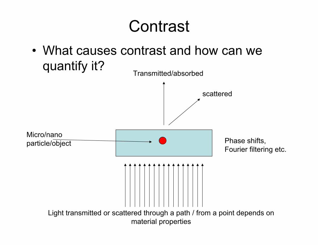
Contrast• What causes contrast and how can we
quantify it?
Micro/nanoparticle/object
Transmitted/absorbed
scattered
Phase shifts,Fourier filtering etc.
Light transmitted or scattered through a path / from a point depends on material properties
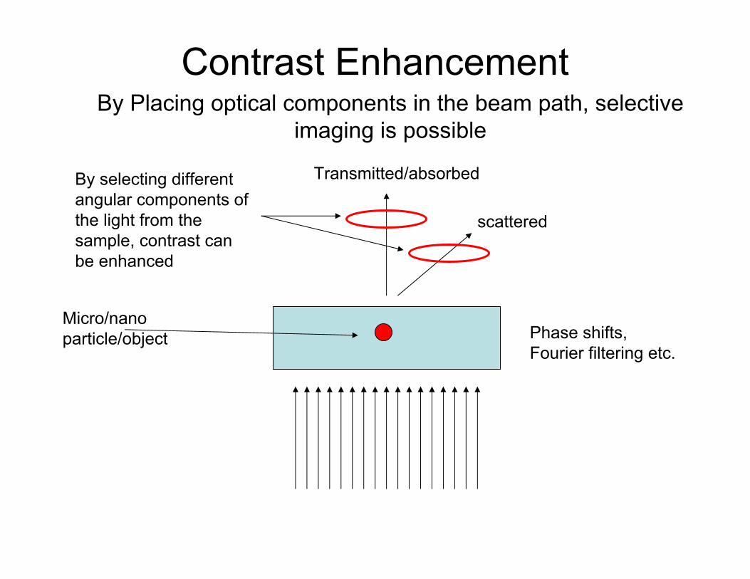
Contrast Enhancement
Micro/nanoparticle/object
Transmitted/absorbed
scattered
Phase shifts,Fourier filtering etc.
By selecting different angular components of the light from the sample, contrast can be enhanced
By Placing optical components in the beam path, selective imaging is possible
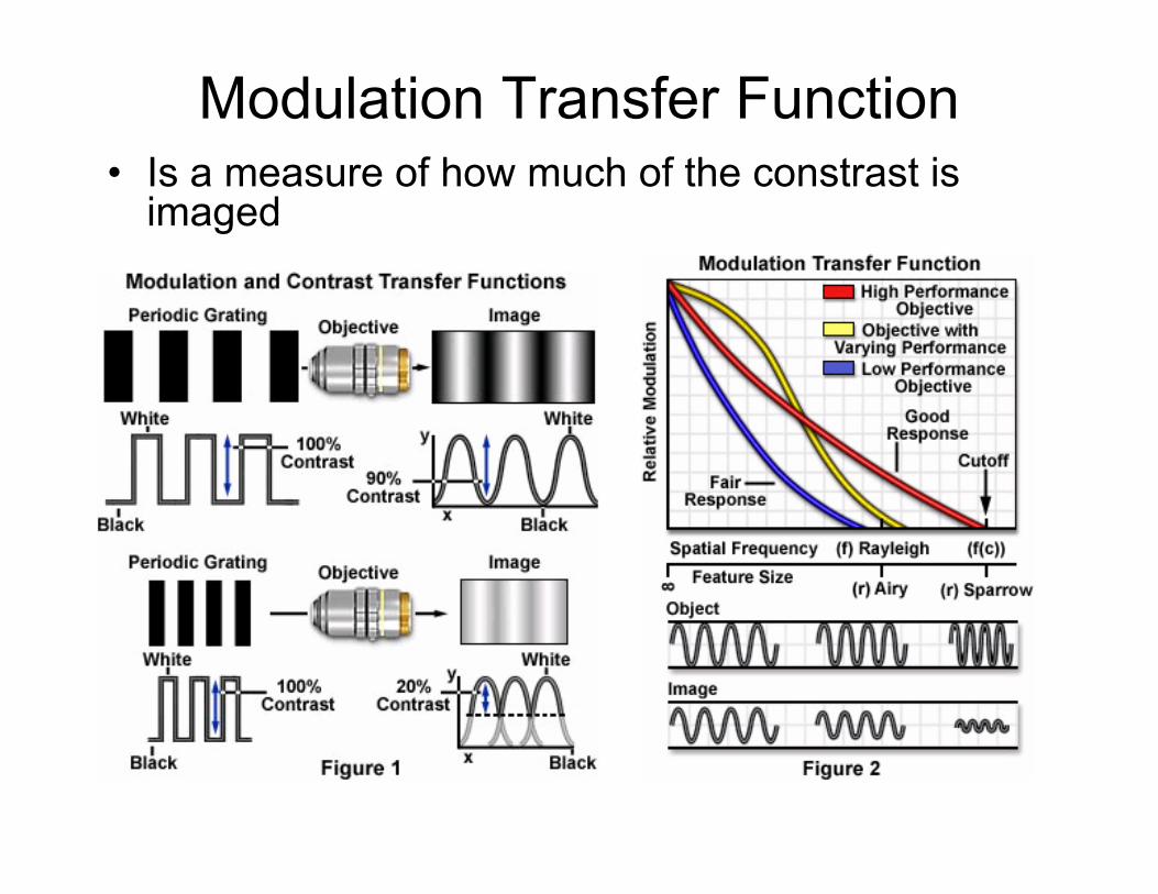
Modulation Transfer Function• Is a measure of how much of the constrast is
imaged
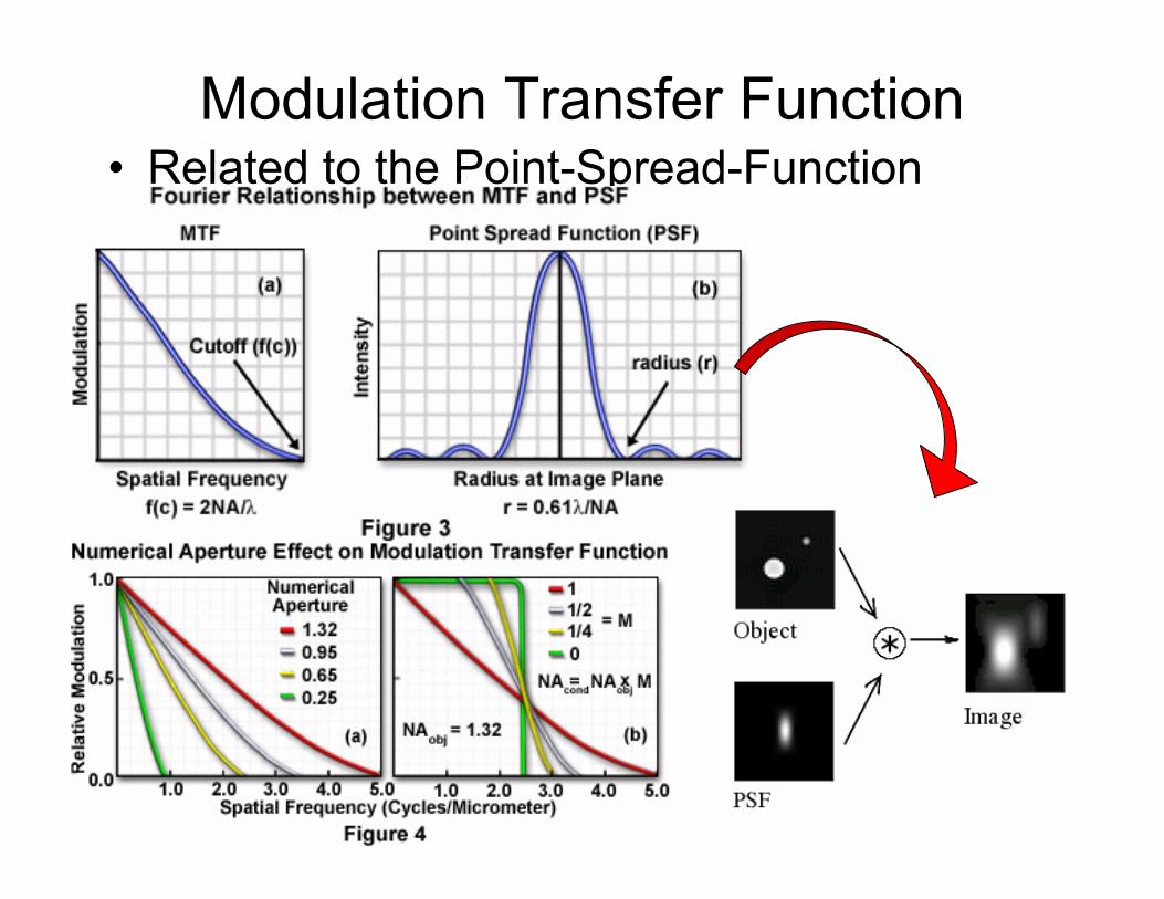
Modulation Transfer Function• Related to the Point-Spread-Function
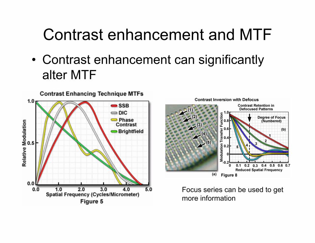
Contrast enhancement and MTF• Contrast enhancement can significantly
alter MTF
Focus series can be used to get more information
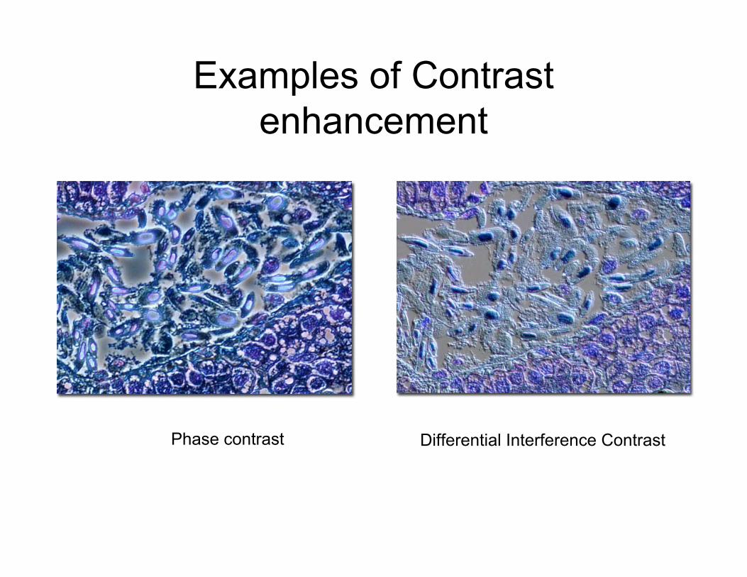
Examples of Contrast enhancement
Phase contrast Differential Interference Contrast
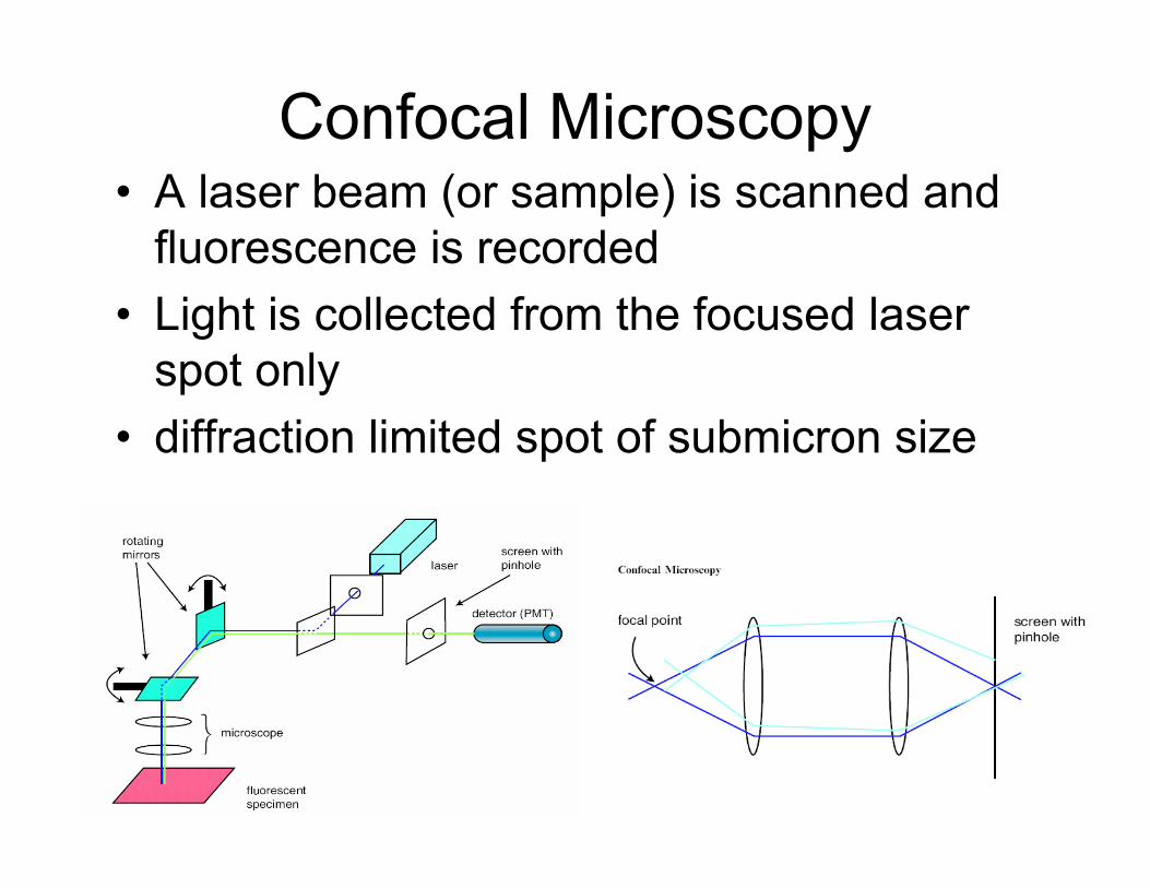
Confocal Microscopy• A laser beam (or sample) is scanned and
fluorescence is recorded• Light is collected from the focused laser
spot only• diffraction limited spot of submicron size
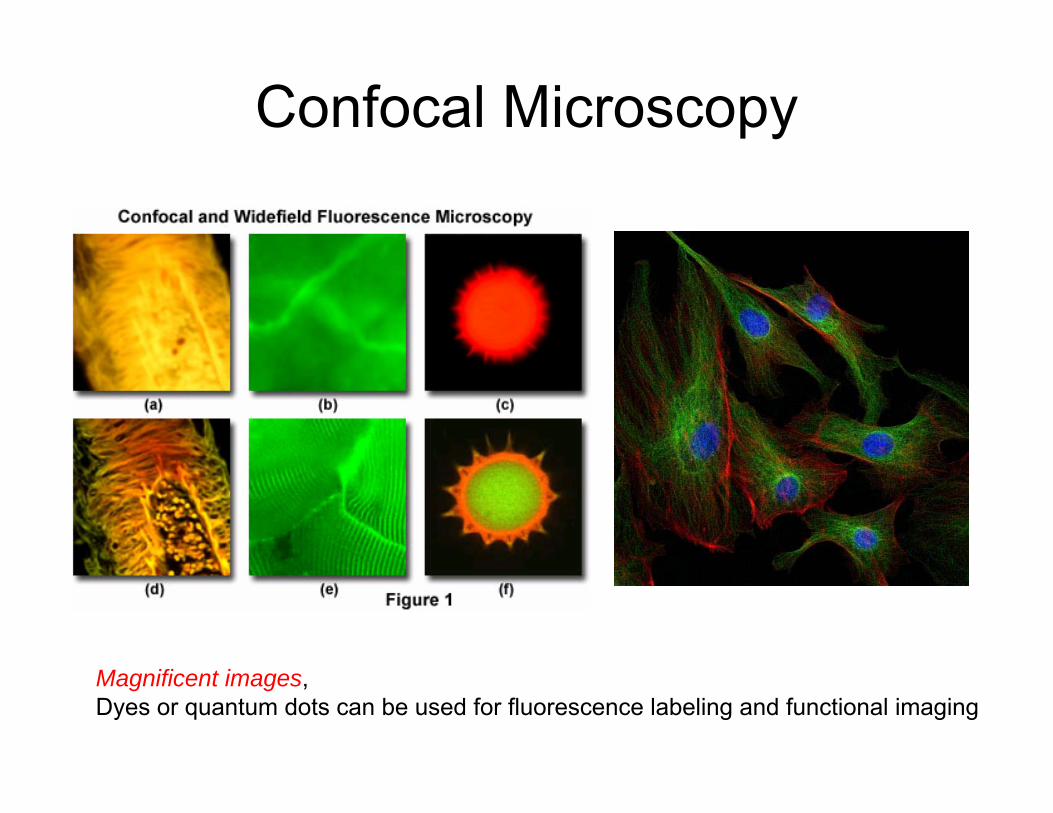
Confocal Microscopy
Magnificent images, Dyes or quantum dots can be used for fluorescence labeling and functional imaging
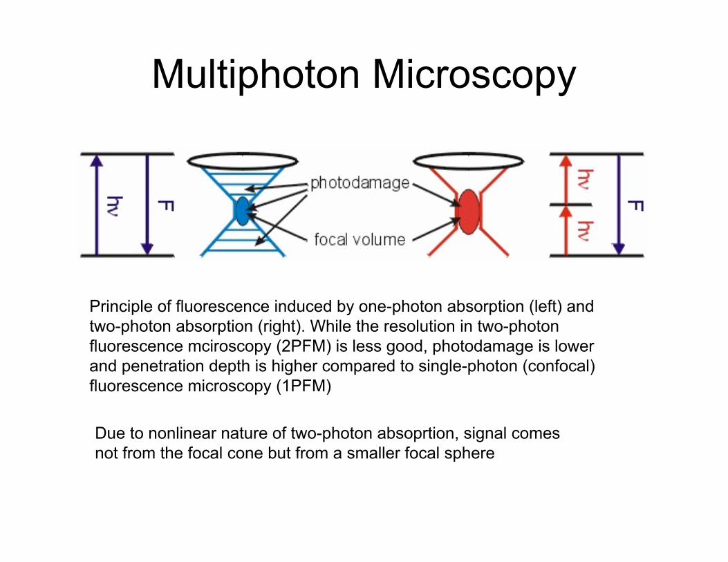
Multiphoton Microscopy
Principle of fluorescence induced by one-photon absorption (left) and two-photon absorption (right). While the resolution in two-photon fluorescence mciroscopy (2PFM) is less good, photodamage is lower and penetration depth is higher compared to single-photon (confocal) fluorescence microscopy (1PFM)
Due to nonlinear nature of two-photon absoprtion, signal comes not from the focal cone but from a smaller focal sphere
Why electron microscopy
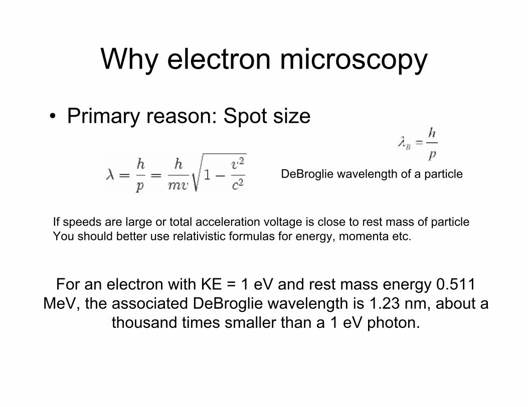
• Primary reason: Spot size
DeBroglie wavelength of a particle
If speeds are large or total acceleration voltage is close to rest mass of particleYou should better use relativistic formulas for energy, momenta etc.
For an electron with KE = 1 eV and rest mass energy 0.511 MeV, the associated DeBroglie wavelength is 1.23 nm, about a
thousand times smaller than a 1 eV photon.
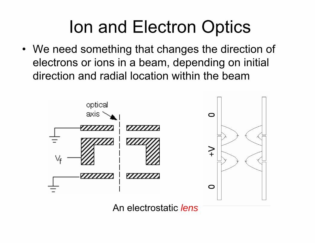
Ion and Electron Optics• We need something that changes the direction of
electrons or ions in a beam, depending on initial direction and radial location within the beam
An electrostatic lens
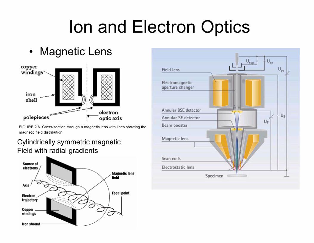
Ion and Electron Optics• Magnetic Lens
Cylindrically symmetric magneticField with radial gradients
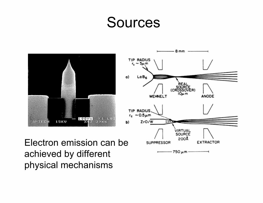
Sources
Electron emission can be achieved by different physical mechanisms
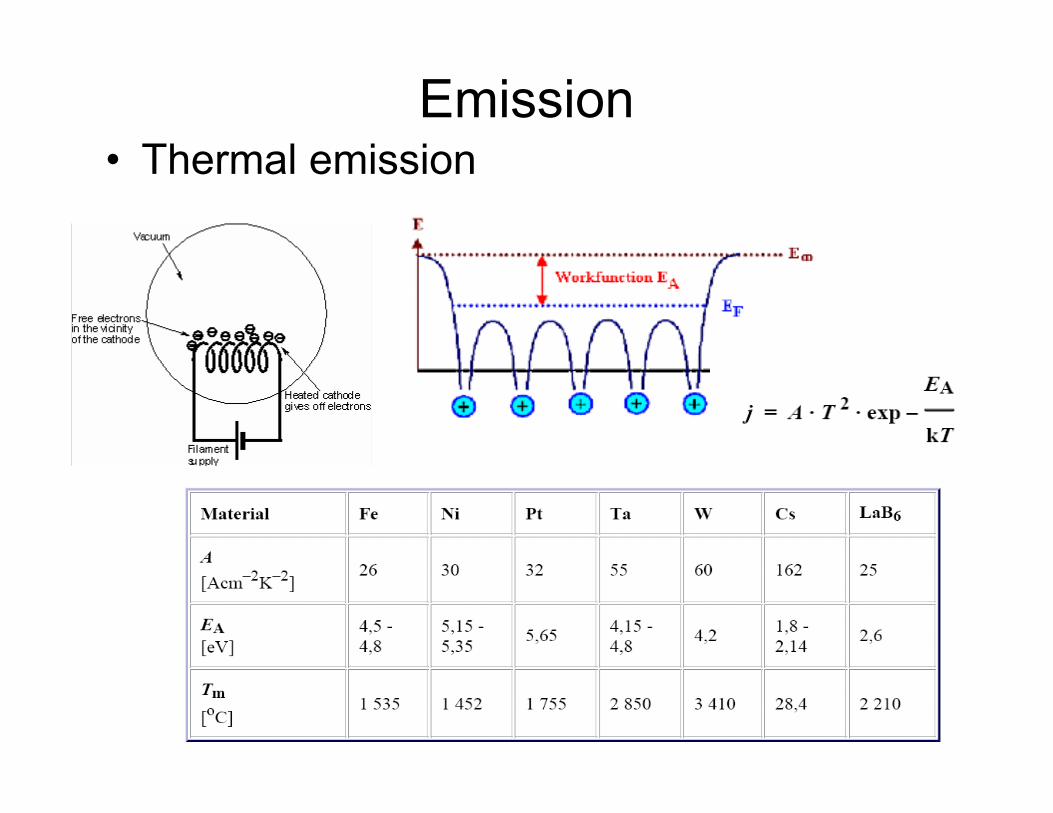
Emission• Thermal emission
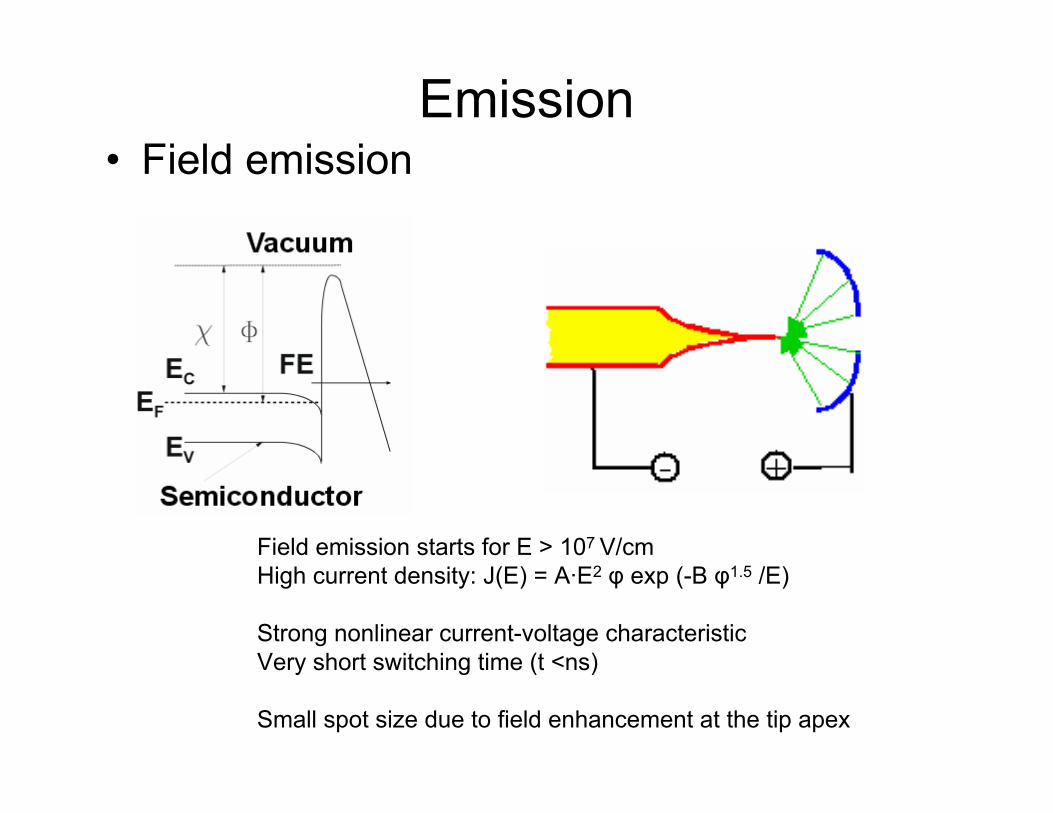
Emission• Field emission
Field emission starts for E > 107 V/cm High current density: J(E) = A·E2 φ exp (-B φ1.5 /E)
Strong nonlinear current-voltage characteristic Very short switching time (t <ns)
Small spot size due to field enhancement at the tip apex
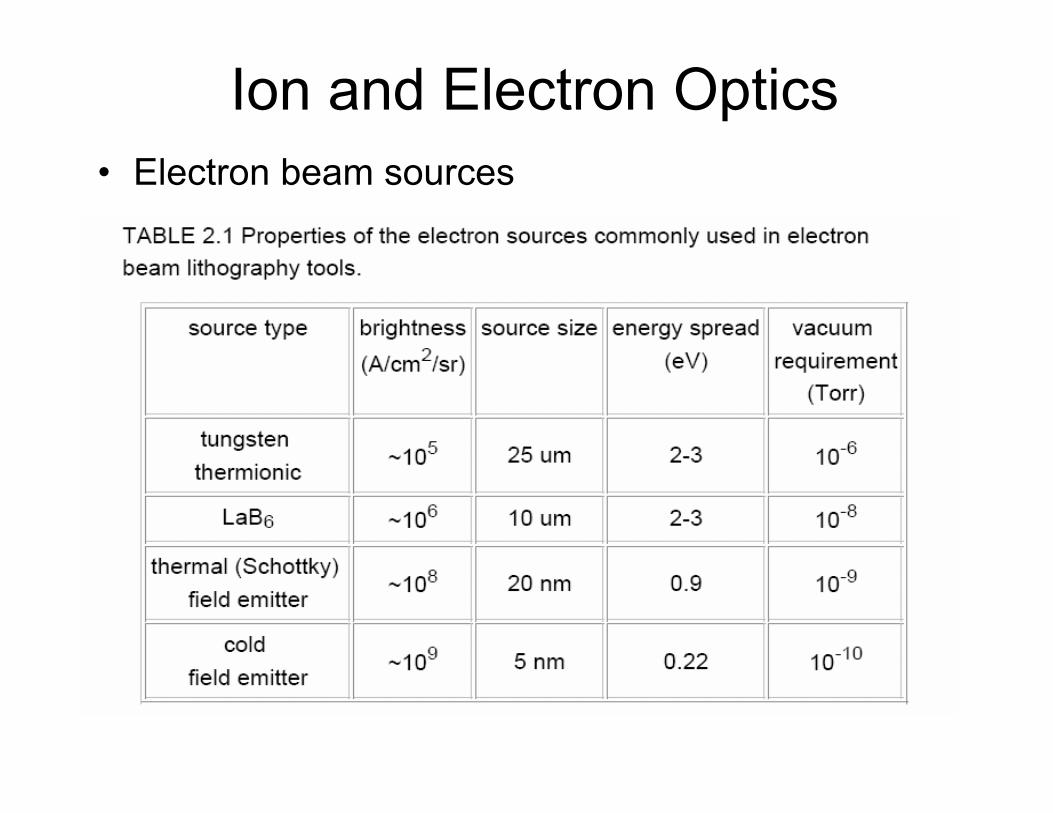
Ion and Electron Optics• Electron beam sources
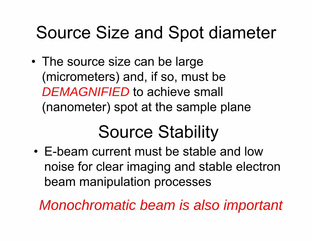
Source Size and Spot diameter• The source size can be large
(micrometers) and, if so, must be DEMAGNIFIED to achieve small (nanometer) spot at the sample plane
Source Stability• E-beam current must be stable and low
noise for clear imaging and stable electron beam manipulation processes
Monochromatic beam is also important
Scanning Electron Microscope
• Sequential imaging similar to the optical scanning confocal microscope
• Can be used in reflection or transmission modes (STEM)
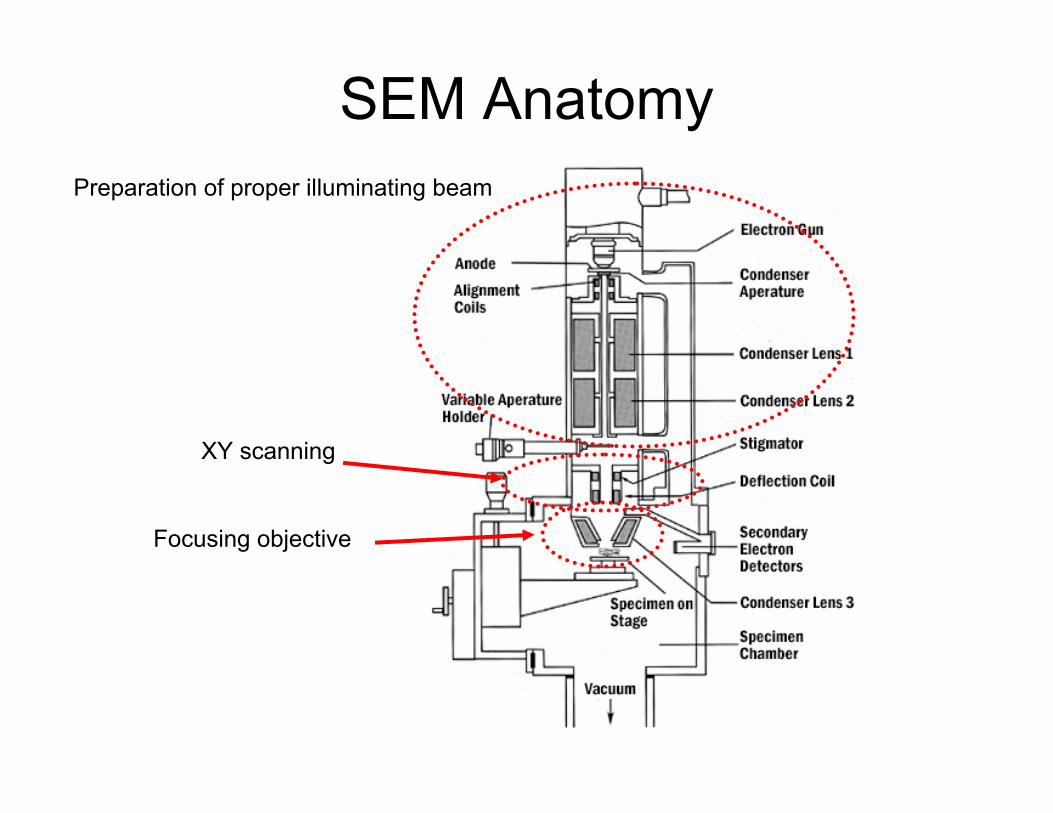
SEM AnatomyPreparation of proper illuminating beam
XY scanning
Focusing objective
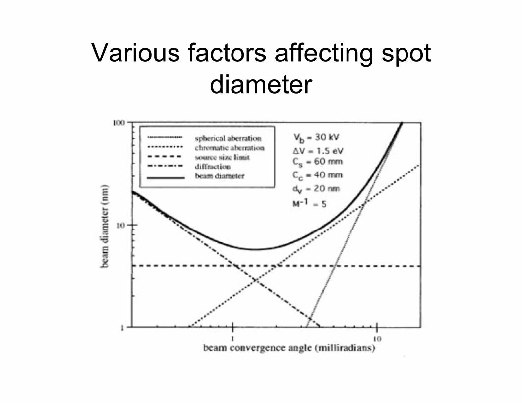
Various factors affecting spot diameter
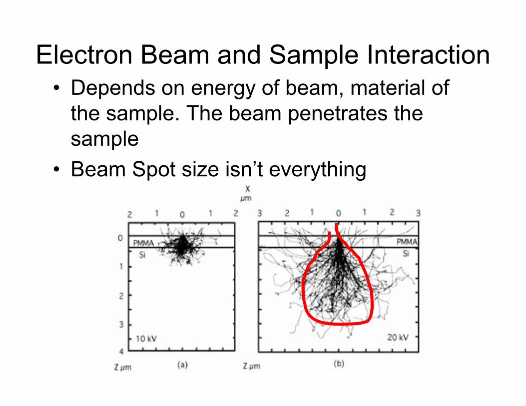
Electron Beam and Sample Interaction• Depends on energy of beam, material of
the sample. The beam penetrates the sample
• Beam Spot size isn’t everything
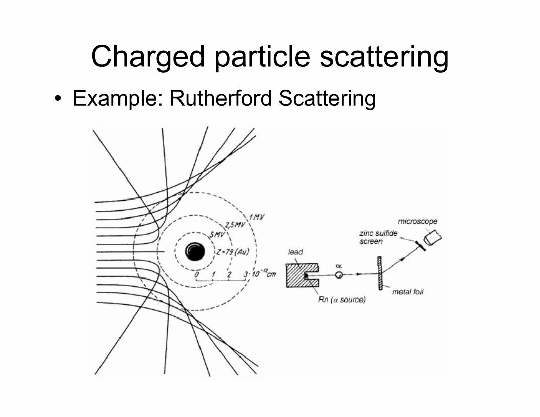
Charged particle scattering• Example: Rutherford Scattering
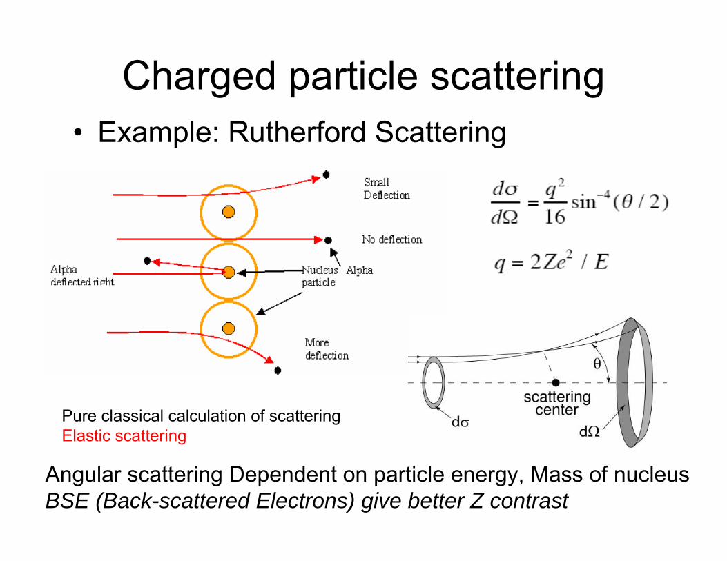
Charged particle scattering• Example: Rutherford Scattering
Angular scattering Dependent on particle energy, Mass of nucleusBSE (Back-scattered Electrons) give better Z contrast
Pure classical calculation of scatteringElastic scattering
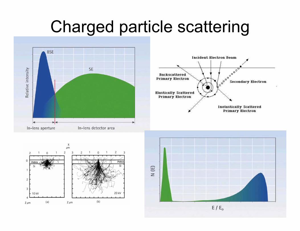
Charged particle scattering
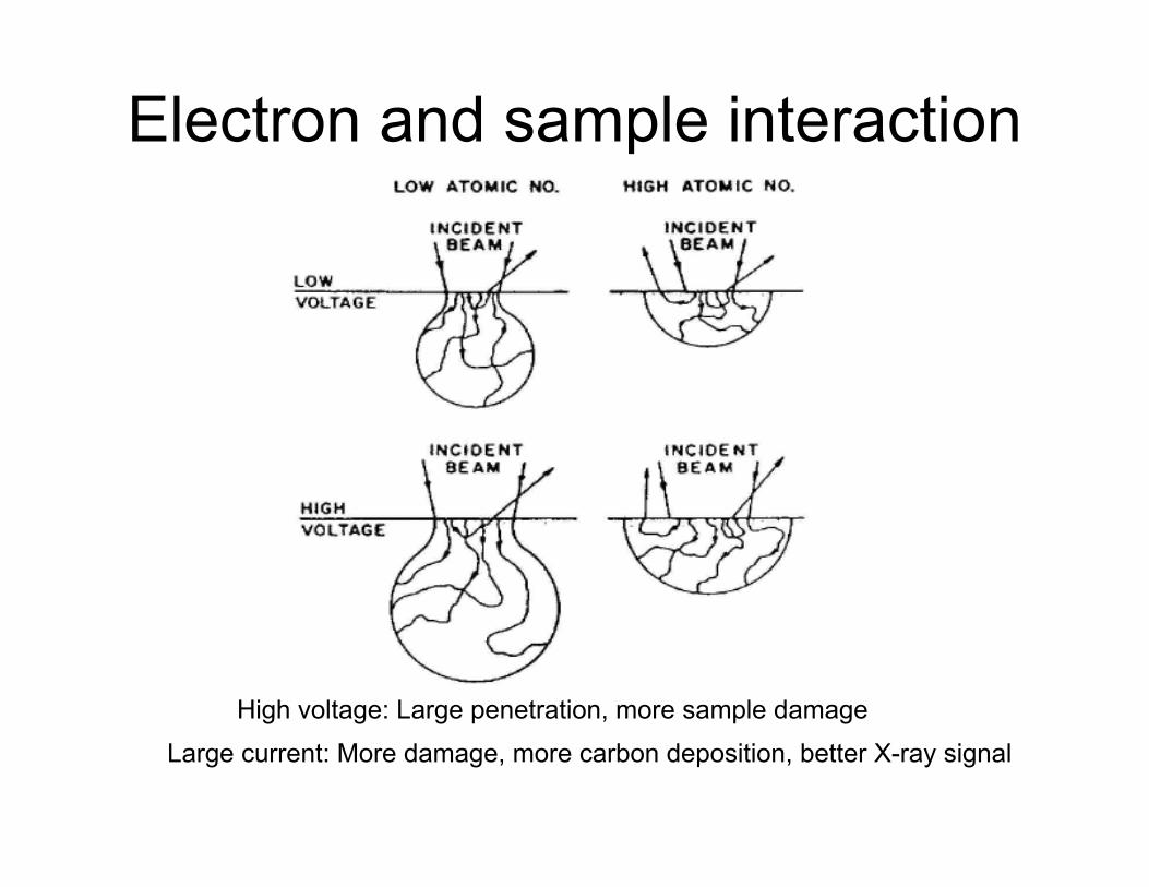
Electron and sample interaction
High voltage: Large penetration, more sample damage
Large current: More damage, more carbon deposition, better X-ray signal
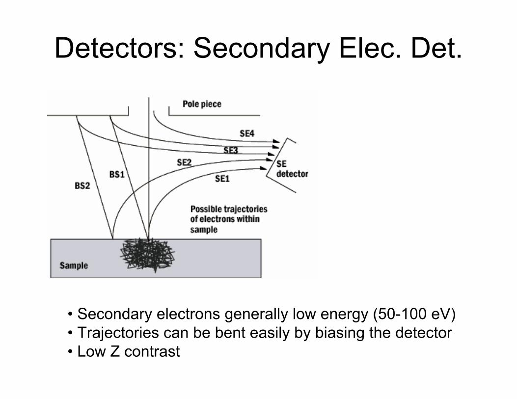
Detectors: Secondary Elec. Det.
• Secondary electrons generally low energy (50-100 eV)• Trajectories can be bent easily by biasing the detector• Low Z contrast
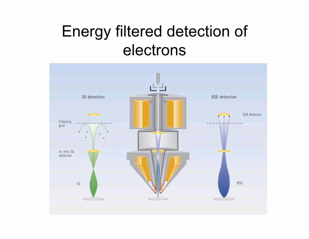
Energy filtered detection of electrons
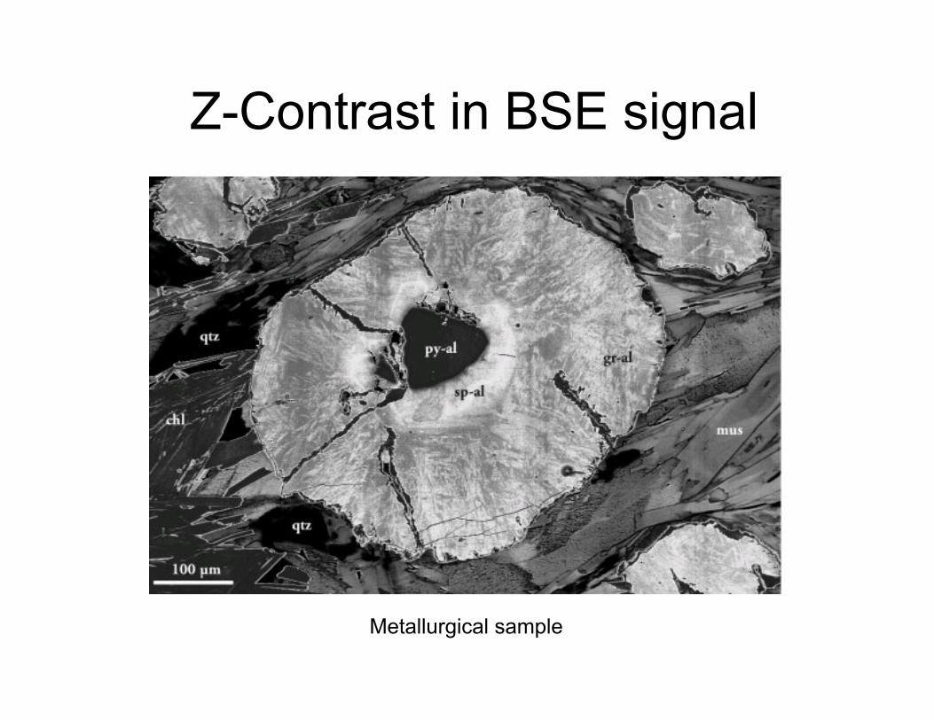
Z-Contrast in BSE signal
Metallurgical sample
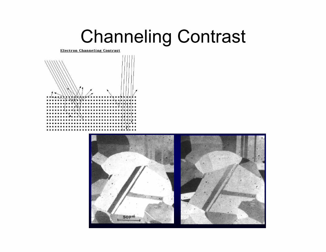
Channeling Contrast
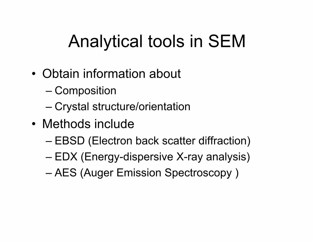
Analytical tools in SEM
• Obtain information about– Composition– Crystal structure/orientation
• Methods include– EBSD (Electron back scatter diffraction)– EDX (Energy-dispersive X-ray analysis)– AES (Auger Emission Spectroscopy )
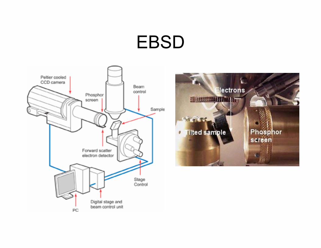
EBSD
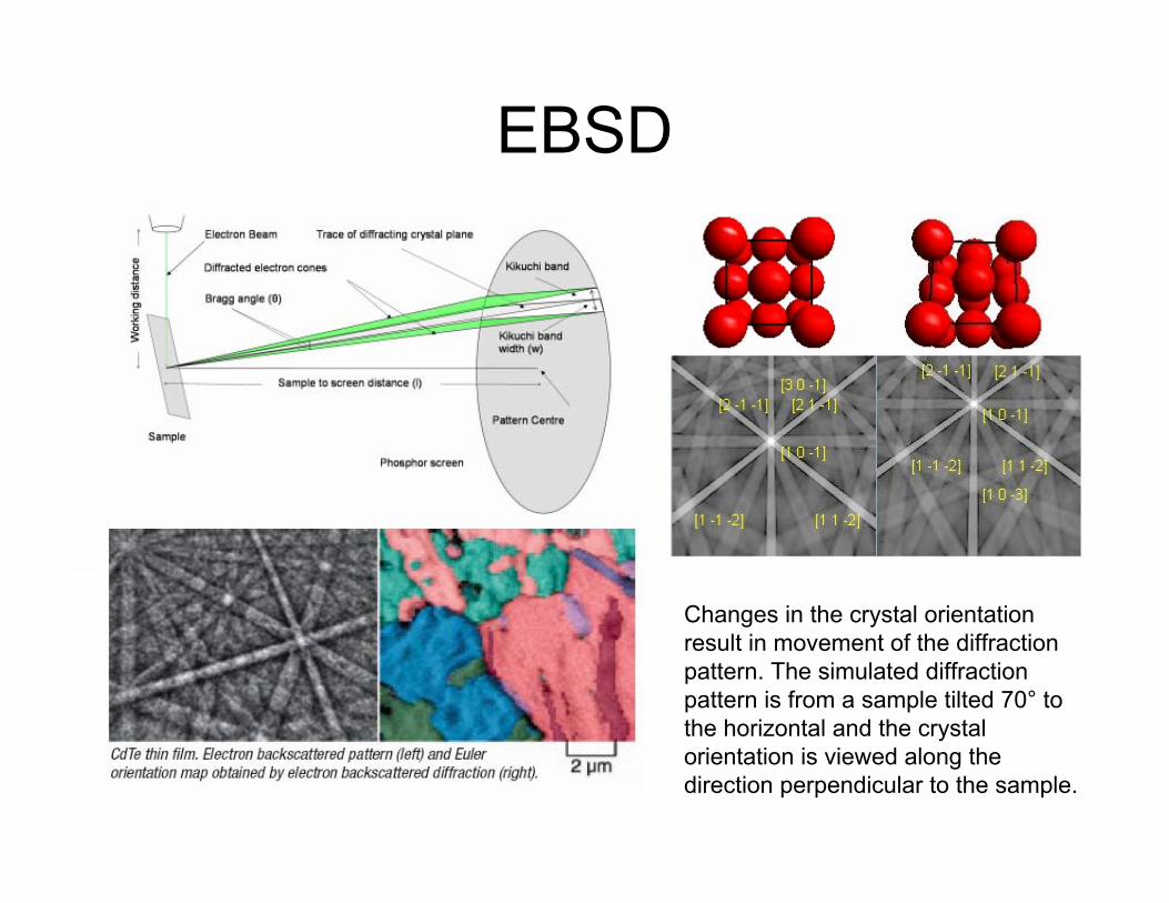
EBSD
Changes in the crystal orientation result in movement of the diffraction pattern. The simulated diffraction pattern is from a sample tilted 70° to the horizontal and the crystal orientation is viewed along the direction perpendicular to the sample.
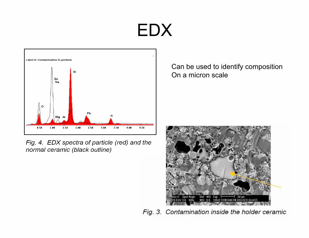
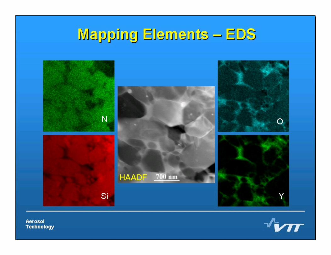
EDX
Can be used to identify compositionOn a micron scale
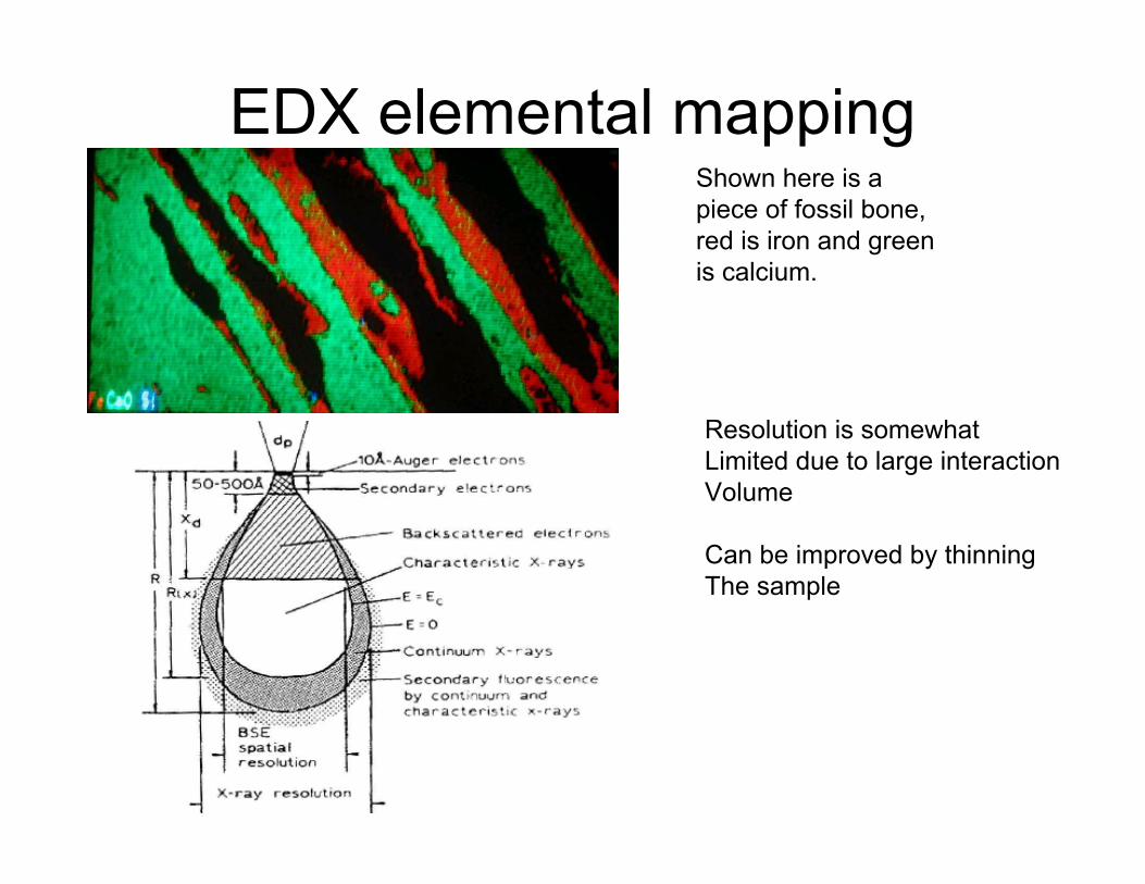
EDX elemental mappingShown here is a piece of fossil bone, red is iron and green is calcium.
Resolution is somewhatLimited due to large interactionVolume
Can be improved by thinning The sample
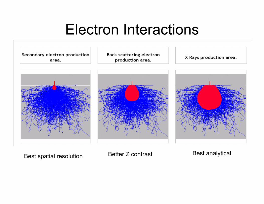
Electron Interactions
Best spatial resolution Better Z contrast Best analytical
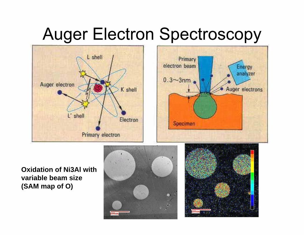
Auger Electron Spectroscopy
Oxidation of Ni3Al with variable beam size (SAM map of O)
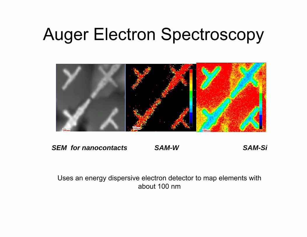
Auger Electron Spectroscopy
SEM for nanocontacts SAM-W SAM-Si
Uses an energy dispersive electron detector to map elements withabout 100 nm
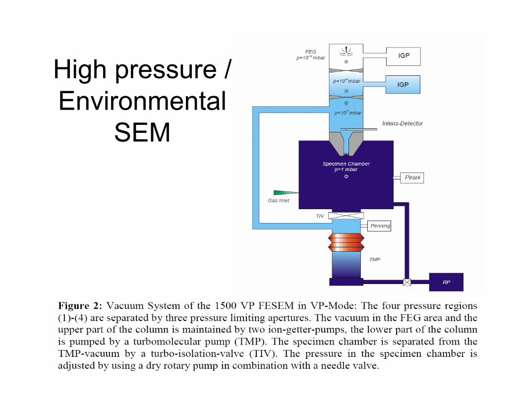
High pressure / Environmental
SEM
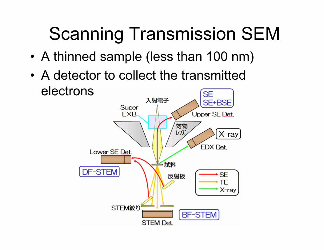
Scanning Transmission SEM• A thinned sample (less than 100 nm)• A detector to collect the transmitted
electrons

Scanning Transmission SEM• For small particulate samples
(biomolecules etc.), use TEM grids
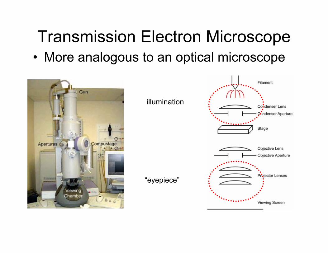
Transmission Electron Microscope• More analogous to an optical microscope
illumination
“eyepiece”
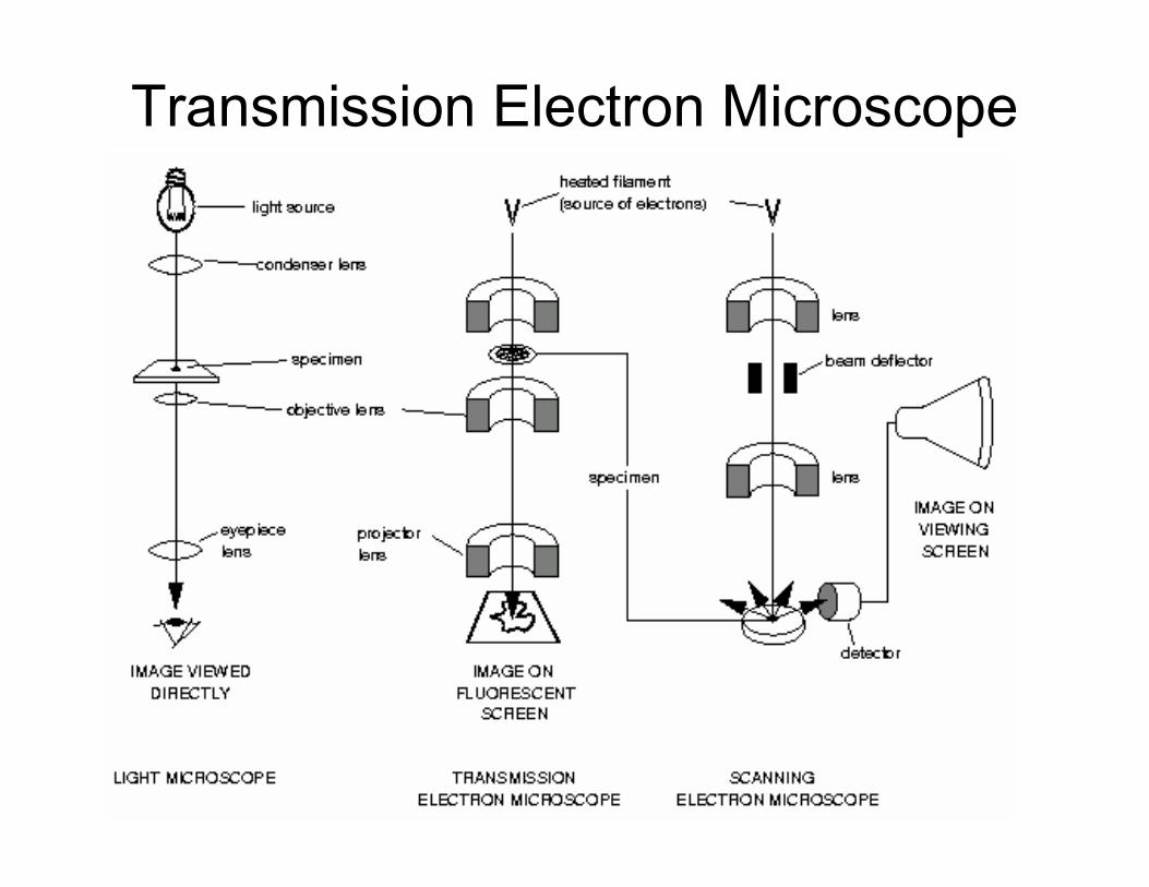
Transmission Electron Microscope
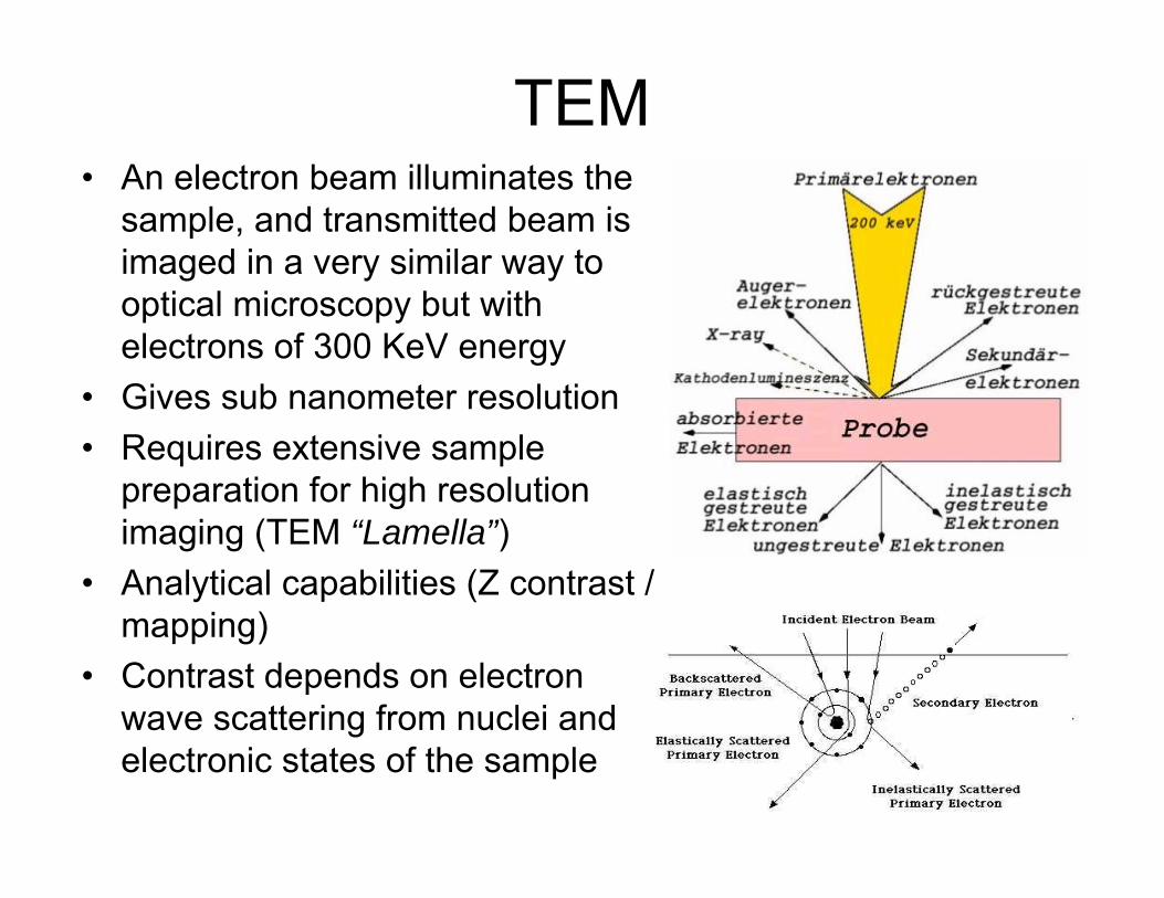
TEM • An electron beam illuminates the
sample, and transmitted beam is imaged in a very similar way to optical microscopy but with electrons of 300 KeV energy
• Gives sub nanometer resolution• Requires extensive sample
preparation for high resolution imaging (TEM “Lamella”)
• Analytical capabilities (Z contrast / mapping)
• Contrast depends on electron wave scattering from nuclei and electronic states of the sample
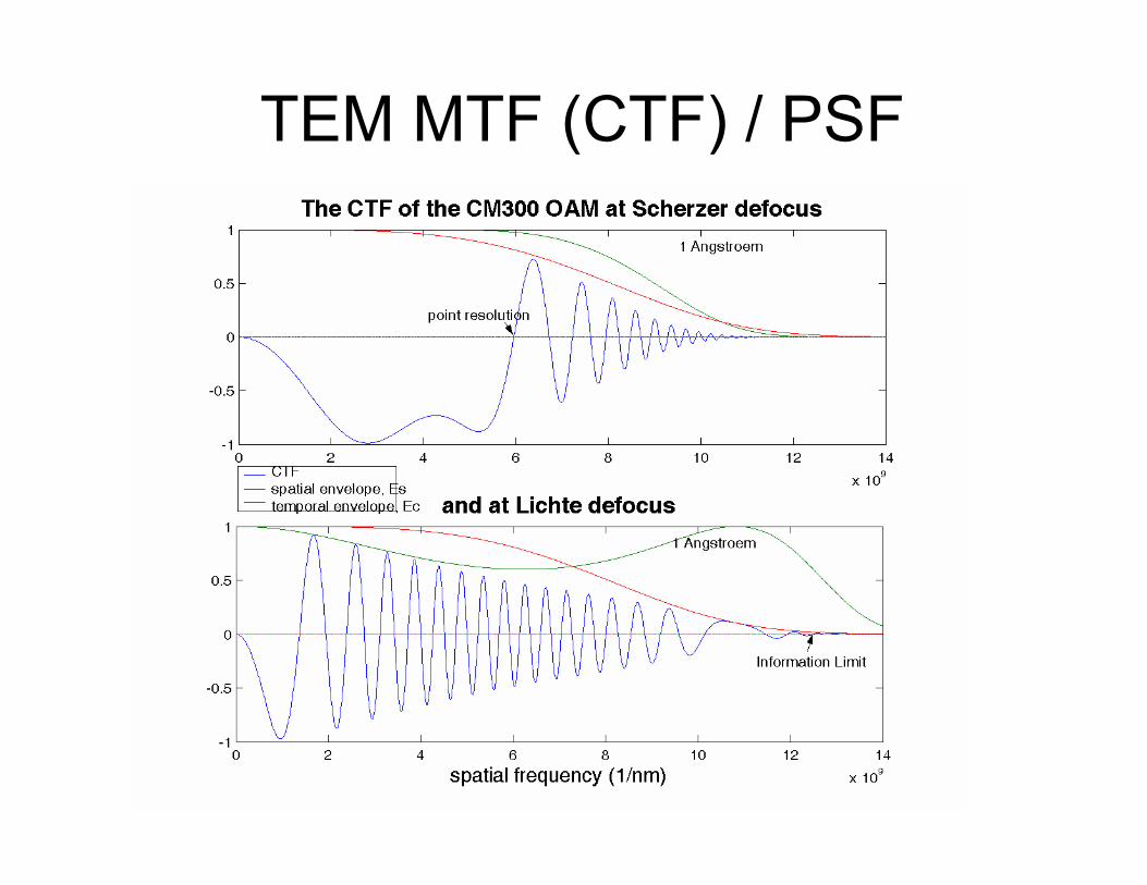
TEM MTF (CTF) / PSF
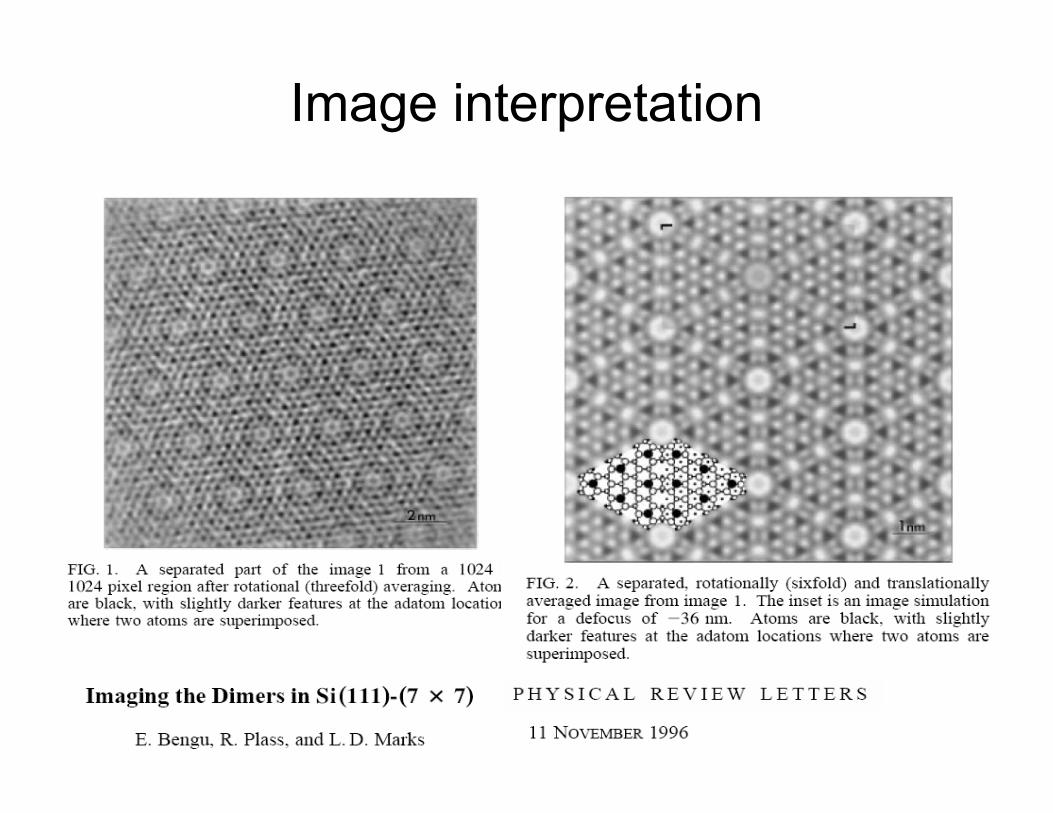
Image interpretation
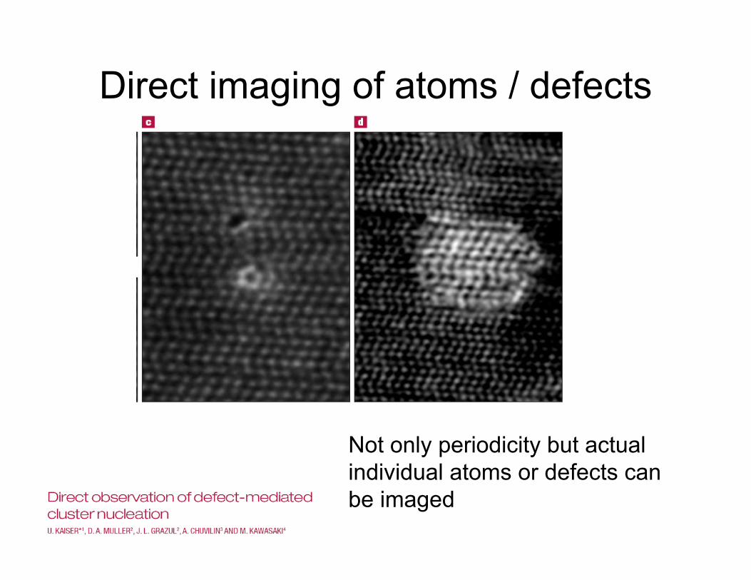
Direct imaging of atoms / defects
Not only periodicity but actual individual atoms or defects can be imaged
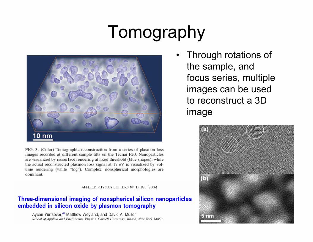
Tomography• Through rotations of
the sample, and focus series, multiple images can be used to reconstruct a 3D image

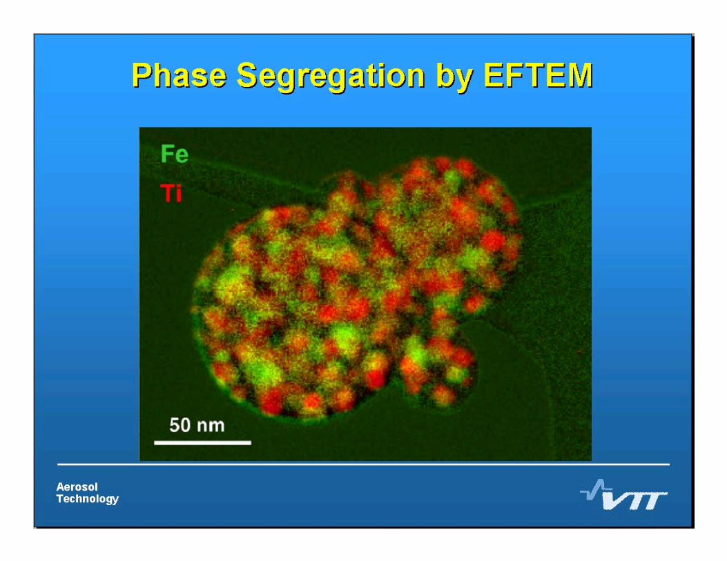
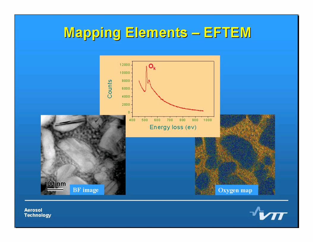
Energy Contrast• Energy loss due to characteristic
electronic properties of material under the beam– Zero-loss– Plasmonic– Core excitations
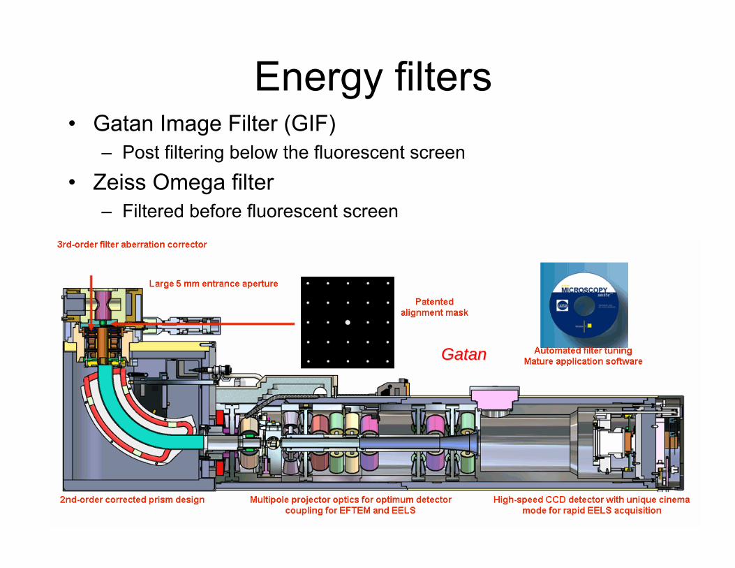
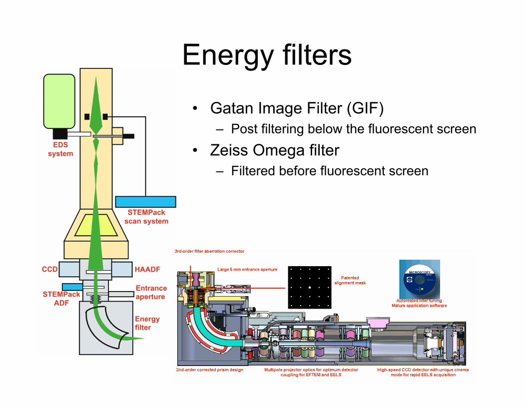
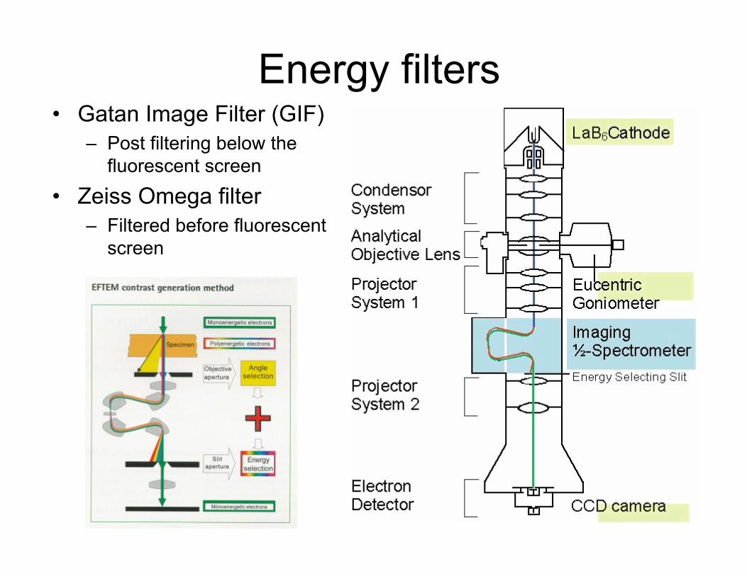
Energy filters• Gatan Image Filter (GIF)
– Post filtering below the fluorescent screen
• Zeiss Omega filter– Filtered before fluorescent screen
GatanGatan
Energy filters
• Gatan Image Filter (GIF)– Post filtering below the fluorescent screen
• Zeiss Omega filter– Filtered before fluorescent screen
Energy filters• Gatan Image Filter (GIF)
– Post filtering below the fluorescent screen
• Zeiss Omega filter– Filtered before fluorescent
screen
Alternative Analytical Tools to EFTEM
• X-Rays!• EDX can be fitted on to a TEM• TEM is operated in a scanning fashion (STEM)
and at each point the X-ray spectrum is recorded to construct an image of elements
• STEM provides better resolution because the sample is already very thin
• Damage to the sample is possible at high energy and high current density
TEM Sample Preparation
• Ultrasonic disk cutters• Abrasive Dimplers• Argon ion gun thinners• Plasma cleaners (to clean thin lamella
surface)• Time consuming process, handwork
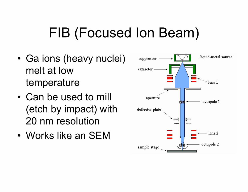
FIB (Focused Ion Beam)
• Ga ions (heavy nuclei) melt at low temperature
• Can be used to mill (etch by impact) with 20 nm resolution
• Works like an SEM
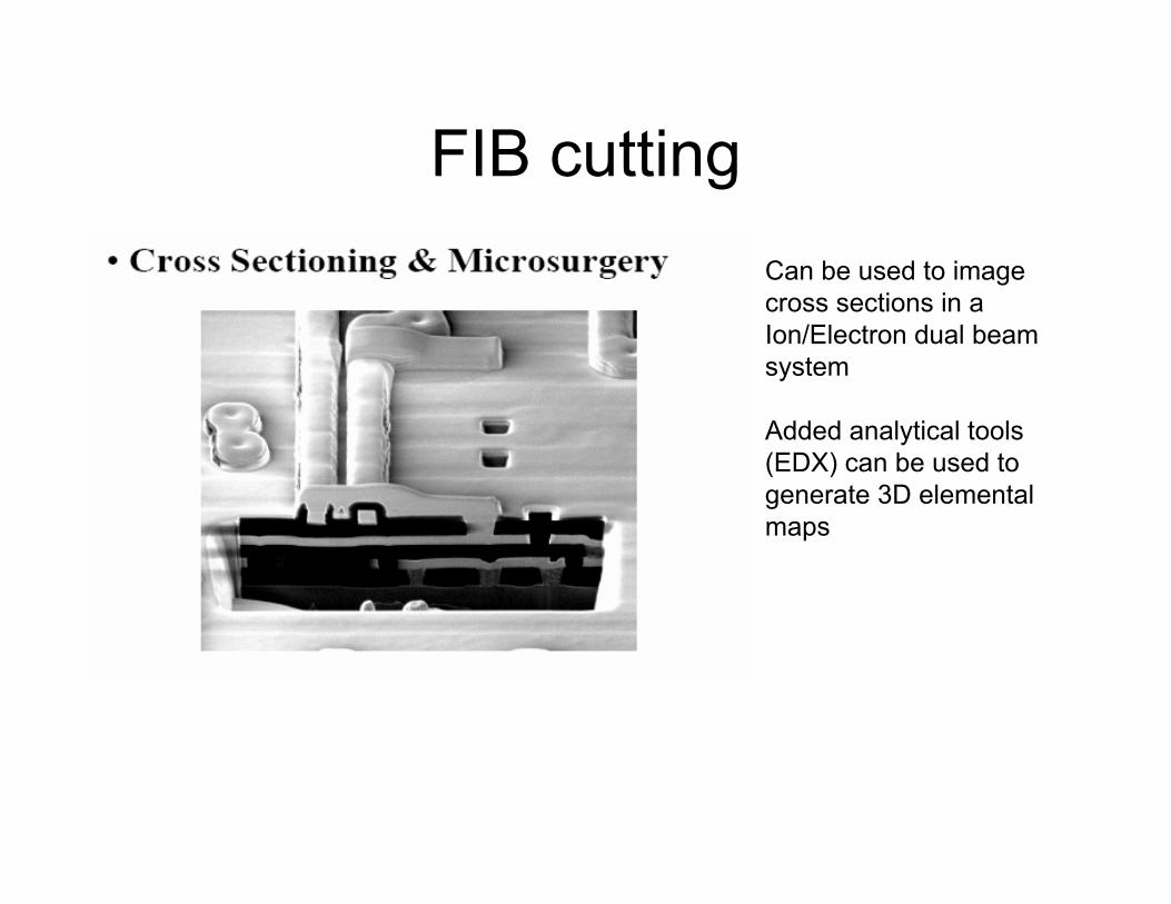
FIB cuttingCan be used to image cross sections in a Ion/Electron dual beam system
Added analytical tools (EDX) can be used to generate 3D elemental maps
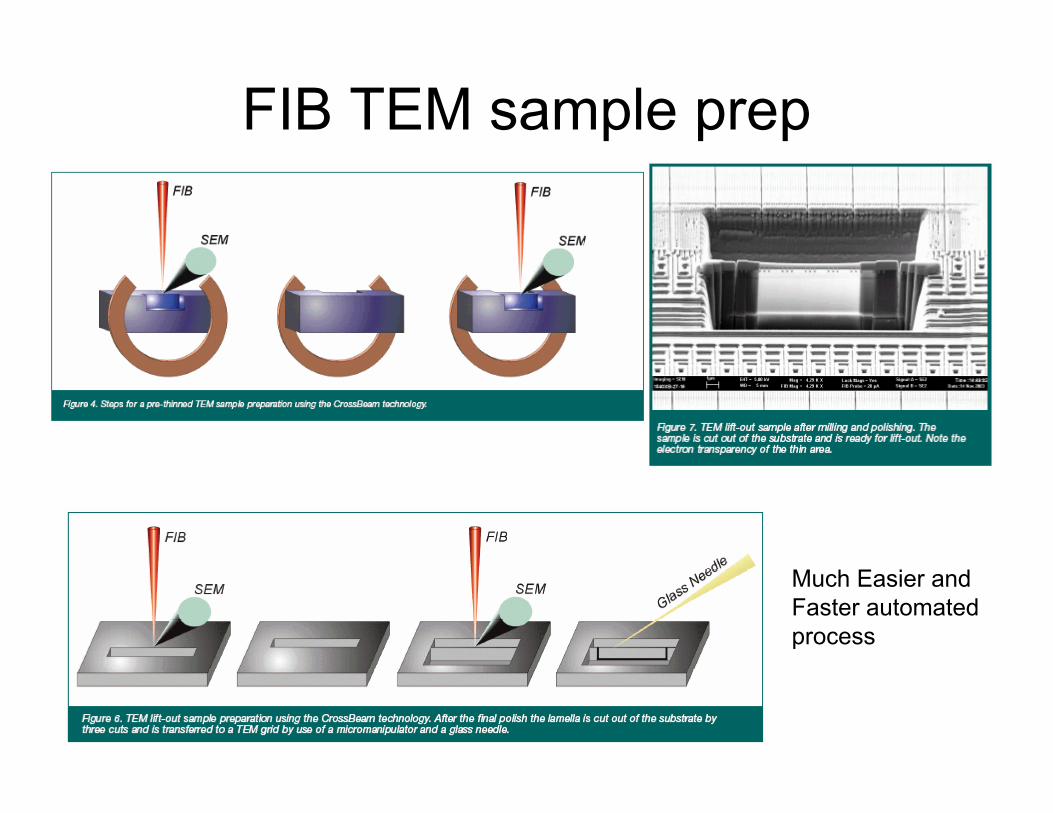
FIB TEM sample prep
Much Easier andFaster automatedprocess
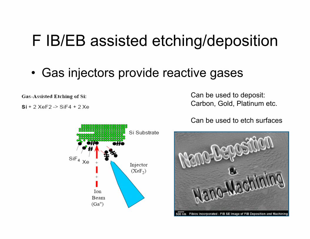
F IB/EB assisted etching/deposition
• Gas injectors provide reactive gasesCan be used to deposit:Carbon, Gold, Platinum etc.
Can be used to etch surfaces
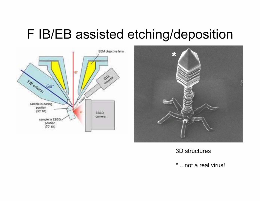
F IB/EB assisted etching/deposition
3D structures
* .. not a real virus!
*
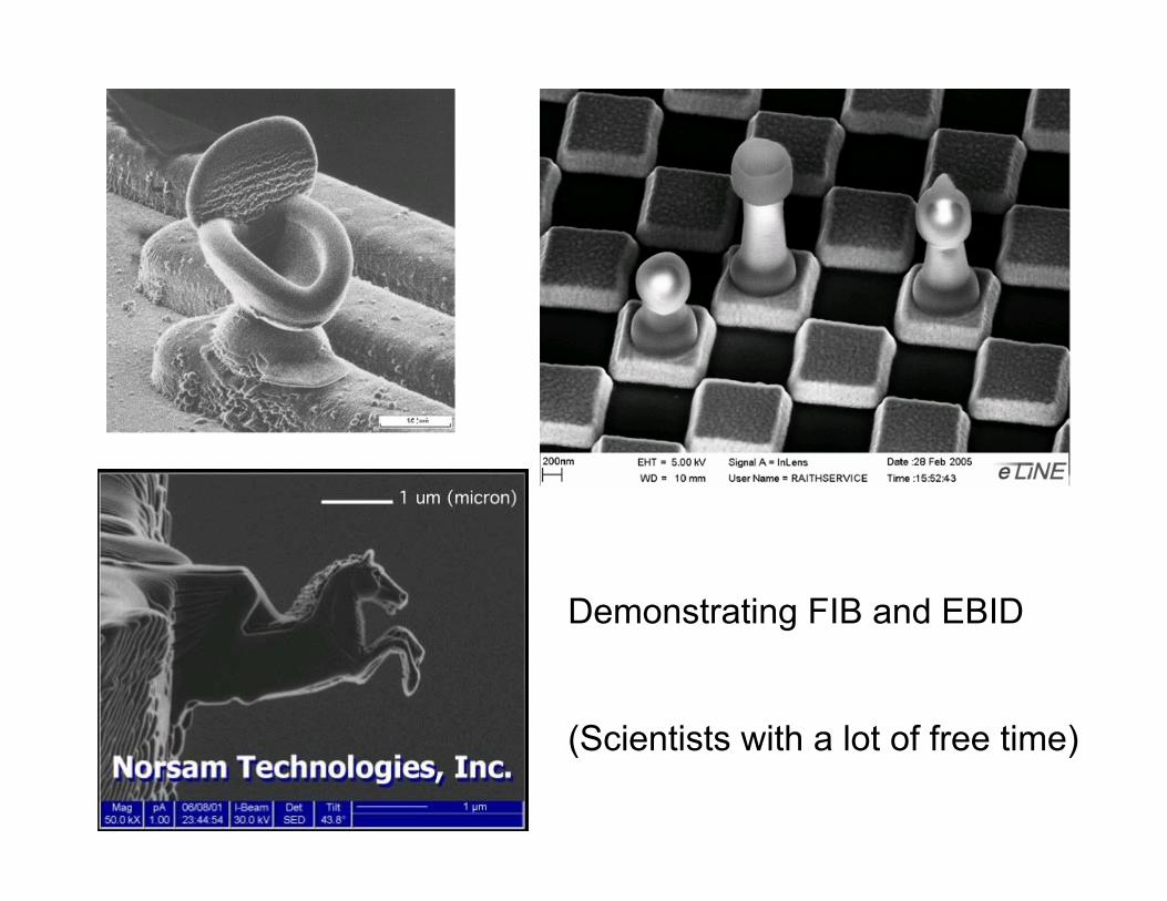
Demonstrating FIB and EBID
(Scientists with a lot of free time)
Recommended