One-Pin 32 kHz Low-Power Crystal Oscillator
A Senior Project
presented to
the Faculty of the Electrical Engineering
California Polytechnic State University, San Luis Obispo
In Partial Fulfillment
of the Requirements for the Degree
Bachelor of Science
by
Aaron Plata-Ruiz
June, 2011
© 2011 Aaron Plata-Ruiz
Plata-Ruiz I
TABLE OF CONTENTS Section Page
I. Introduction .............................................................................................................................. 1 II. Background .......................................................................................................................... 3
A. Oscillator Circuits ................................................................................................................ 3 B. Barkhausen Criteria for Oscillation ..................................................................................... 3 C. RC and LC Tuned Oscillators .............................................................................................. 4 D. Crystal Oscillators ................................................................................................................ 5
III. Requirements ....................................................................................................................... 8 IV. Design .................................................................................................................................. 9
A. Crystal Oscillator System .................................................................................................... 9 B. Crystal Oscillator Subcircuit ................................................................................................ 9
1. Crystal Component Modeling .......................................................................................... 9 2. Crystal Oscillator Circuit Configuration ........................................................................ 12 3. Crystal Oscillator Impedance Analysis .......................................................................... 15 4. Crystal Oscillator Small Signal Analysis ....................................................................... 18 5. Crystal Oscillator Large Signal Analysis ....................................................................... 21
C. Computer Simulation ......................................................................................................... 23 V. Test Plan............................................................................................................................. 30 VI. Development and Construction.......................................................................................... 31 VII. Integration and Test Results ............................................................................................... 33 VIII. Conclusion and Recomendations ................................................................................... 35 IX. Bibliography ...................................................................................................................... 36 X. Appendices ......................................................................................................................... 37
A. Schematic ........................................................................................................................... 38 B. Part List, Cost, and Time Schedule Allocation .................................................................. 39 C. Circuit Layout .................................................................................................................... 41 D. Program Listing ................................................................................................................. 49
Plata-Ruiz II
LIST OF TABLES AND FIGURES LIST OF TABLES Table 1 Crystal Component Parameters ....................................................................................................................... 9 Table 2 Calculated crystal model parameters. ............................................................................................................ 12 Table 3 Calculated crystal impedances ideal circuit impedances. .............................................................................. 18 Table 4 Calculated small signal model parameters. .................................................................................................... 21 Table 5 Calculated large signal crystal model parameters. ......................................................................................... 22 Table 6 Calculated circuit bias current at adjusted transconductance. ........................................................................ 29 LIST OF FIGURES Figure 1 Basic Feedback Circuit ................................................................................................................................... 3 Figure 2 One-Pin Connection Configuration ................................................................................................................ 6 Figure 3 One-Pin Circuit with XTAL Model ............................................................................................................... 6 Figure 4 Ideal Condition for Oscillation ....................................................................................................................... 7 Figure 5 Crystal Oscillator System ............................................................................................................................... 9 Figure 6 Fundamental mode crystal circuit model ..................................................................................................... 10 Figure 7 Crystal model with component values. ........................................................................................................ 11 Figure 8 Simulation of crystal model between series and parallel frequencies. ......................................................... 12 Figure 9 Basic Colpitts oscillator configuration for NMOS ....................................................................................... 13 Figure 10 Basic Colpitts oscillator configuration for PMOS ...................................................................................... 14 Figure 11 Colpitts oscillator NMOS configuration with biasing circuit. .................................................................... 14 Figure 12 Colpitts oscillator configuration with crystal model. ................................................................................. 15 Figure 13 Colpitts oscillator with crystal model and circuit transconductance. ......................................................... 17 Figure 14 Crystal oscillator small signal model. ........................................................................................................ 18 Figure 15 Crystal oscillator small signal model expanded. ........................................................................................ 19 Figure 16 Simplified crystal oscillator small signal model. ........................................................................................ 19 Figure 17 Complex loop gain root locust at critical transconductance. ...................................................................... 23 Figure 18 Loop gain and total loop phase shift at critical transconductance. ............................................................. 24 Figure 19 Complete crystal oscillator schematic. ....................................................................................................... 25 Figure 20 Crystal oscillator initial -second simulation. .............................................................................................. 25 Figure 21 Crystal oscillator simulation at resonance transition region. ...................................................................... 26 Figure 22 Crystal oscillator simulation at startup. ...................................................................................................... 26 Figure 23 Crystal oscillator simulation at steady state. .............................................................................................. 27 Figure 24 Loop gain vs transconductance at critical transconductance. ..................................................................... 27 Figure 25 Loop gain vs transconductance at adjusted transconductance. ................................................................... 28 Figure 26 Complex loop gain root locust at adjusted transconductance. .................................................................... 28 Figure 27 Loop gain and total loop phase shift at adjusted transconductance. ........................................................... 29 Figure 28 Crystal oscillator circuit implemented on a breadboard. ............................................................................ 32 Figure 29 Crystal oscillator circuit implemented on a copper ground plane. ............................................................. 32 Figure 30 Crystal oscillator test setup. ........................................................................................................................ 33 Figure 31 Lab test setup. ............................................................................................................................................. 34

Plata-Ruiz III
ACKNOWLEDGEMENTS
I would like to thank first of all my wife Claudia for all her patience, understanding, and
sacrifice, so I could complete this project on time. I would also like to thank Ali E. Zadeh for
mentoring me and giving me the original idea for this project in order to learn about crystal
oscillators. I would like to also thank St. Jude Medical management, including Jonathan Losk,
Dro Darbidian, Gabriel Mouchawar, and Ariel Kopelioff for their support and encouragement to
finish my EE degree. And last but not least, I would like to thank Dr. Dennis Derickson for
accepting me as my senior advisor and encouraging me to pursue a Senior Project topic with
substance that would benefit my career.
Plata-Ruiz IV
ABSTRACT
For this senior project, I designed a one-pin, 32 kHz, low-power, crystal oscillator suitable for
battery-operated systems. The design is based on a design published by Ali E Zadeh, “A
Micropower, Battery-Operated, One-Pin Crystal Oscillator”, but redesigned for standard positive
power supply configuration, which is suitable for typical n-well CMOS process. Yet, due to time
constraints, the design was implemented using off-the-shelf discrete CMOS components. The
activities required for this project included research, requirements definition, design and
simulation, assembly, test design implementation. The skills required included but were not
limited to small-signal and large-signal circuit model analysis, control circuit analysis, time-
domain analysis, and frequency-domain analysis.
Plata-Ruiz 1
I. Introduction
One of the most ubiquitous and essential components modern computing systems is the real time
clock circuit, which is used to track time and in some occasions is realized using a crystal
oscillator and a comparator. For most applications, the clock must be highly accurate and should
keep that accuracy regardless of fluctuations in electrical power, temperature, mechanical
disturbances, electromagnetic noise, etc. In addition, the clock must be able to reliably start
every single time upon system power up and be ready within a reasonable short time.
Furthermore, for portable, battery-operated applications, it is desirable that the clock circuitry
minimizes power consumption down to the micro-power range, if not even lower. Last but not
least, to optimize manufacturability and maximize reliability, it is also desired to have a clock
circuit that minimizes its component count, its system footprint, and its connection count.
The heart of the clock circuit is the crystal oscillator. Therefore, the main purpose of this report
is to document the process of defining, designing, developing, implementing, integrating, and
testing a one-pin, 32 kHz, low-power crystal oscillator that is suitable for battery operation and
that could be implemented using a standard n-well CMOS process. The circuit implementation
for this Senior Project was limited to the prototype level using MOSFET discrete devices to meet
the requirement that a circuit be built for demonstration purposes within the time frame of the
project.
This document is organized in seven main sections: the Background, which briefly describes the
basic theory behind crystal oscillators within the perspective of this project; the Requirements
section, which defines the minimum set of requirements that the product should meet; the
Design section, which documents the decisions made to synthesize the requirements into a

Plata-Ruiz 2
system; the Test Plan section, which describes the set of tests required to verify the system’s
performance against the requirements; the Development and Construction section, which
documents the process to realize the system into a physical product; the Integration and Test
Results section, which documents the product’s test verification results; and the Conclusion
section, which documents the product’s overall analysis and recommendations for future
implementations.
Plata-Ruiz 3
II. Background
A. Oscillator Circuits
Oscillators are signal-generating, feedback circuits that can be classified [4] in two general
classes: Tuned Oscillators and Un-tuned Oscillators. Tuned Oscillators are circuits designed to
oscillate, or resonate, to one particular frequency, and include RC, LC, and Crystal Oscillators.
These circuits are suitable for accurate time-base applications such as a clock signal sources for
computer systems. Un-tuned Oscillators include Triangle, Sinusoidal, and Squarewave
Oscillators, all of which have diverse applications. For example, a sinusoidal oscillator circuit
may be designed so the output frequency is a function of an input voltage; such a circuit is
known as a Voltage Controlled Oscillators (VCO) and it has many applications in
communication systems.
B. Barkhausen Criteria for Oscillation
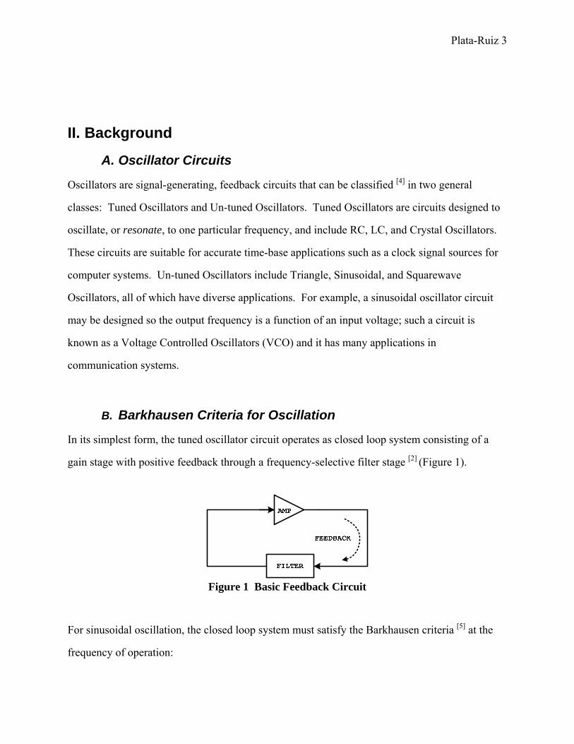
In its simplest form, the tuned oscillator circuit operates as closed loop system consisting of a
gain stage with positive feedback through a frequency-selective filter stage [2] (Figure 1).
Figure 1 Basic Feedback Circuit
For sinusoidal oscillation, the closed loop system must satisfy the Barkhausen criteria [5] at the
frequency of operation:

Plata-Ruiz 4
The loop gain must be unity for ideal sinusoidal oscillation.
The total loop phase shift must be equal to 0° or even multiples of 360°.
Ideally, at the frequency of operation, the amplifier stage provides the unity gain plus the first
180° in loop phase shift, while the positive feedback filter stage provides the second 180° in loop
phase shift. In addition, ideal sinusoidal oscillation occurs with unity loop gain; whereas any
loop gain higher than unity causes distortion of the sinusoidal output. Nevertheless, in practice,
the loop gain must be set slightly higher than unity to compensate for resistive losses in the
circuit but not as high to minimize signal distortion.
Oscillation in real circuits is spontaneously initiated by the by tiny transient signals and/or noise
generated during the power up event. The frequency-selective circuit resonates with the signal at
the frequency of operation and amplifies it many times around the loop until non-linear effects in
the circuit limit the amplitude. At this point the oscillation reaches steady-state.
C. RC and LC Tuned Oscillators
As its name suggests, the RC or LC tuned oscillator uses capacitors, inductors, and/or resistors in
the frequency-selective filter network, which ideally resonates to the desired frequency of
operation. In practice, this resonance may occur within a very narrow frequency bandwidth
determined by the filter’s figure of merit, or quality factor, Q, which quantifies the resistive
energy loss and is defined as the ratio of the filter’s reactance to its resistance. For quality
factors of 10 or greater, this bandwidth can be found by the calculating the ratio of the frequency
of operation to the quality factor [2].
There are many basic tuned oscillator circuit topographies available, including countless of
iterations. Tuned RC oscillator circuits are suitable for low frequency operation and may
Plata-Ruiz 5
incorporate op-amps for gain; examples of classic RC oscillator circuits include Wien-Bridge,
Quadrature, and Phase-Shift oscillator topographies. Tuned LC oscillator circuits are realized
with individual transistors for gain, and due to the high-Q frequency-selective feedback filter
network, they are suitable for higher frequencies; examples of classic LC oscillator circuits
include Colpitts, Hartley, and Pierce oscillator topographies. It is worth to mention that one
main disadvantage of RC/LC tuned oscillators is that the frequency of oscillation may drift due
to changes in temperature, power supply voltage, or mechanical disturbances. For this reason,
these circuits usually require manual tuning [2].
D. Crystal Oscillators
The Crystal Oscillator can be considered as a type of tuned LC oscillator in which a two-lead
quartz crystal component is incorporated by the frequency-selective LC filter network [5]. The
quartz crystal is a material with piezoelectric properties that exhibits a very high quality factor,
Q > 10,000, at the frequency of operation. A piezoelectric material is one that converts electrical
energy from an applied electric field into mechanical energy as a displacement. When the field
is removed, the stored mechanical energy is converted back to electrical energy as an electric
field. With respect to the crystal oscillator circuit operation, when a DC voltage is applied across
the crystal it vibrates with a frequency determined by the crystal’s characteristics and this
vibration is seen by the circuit as a small AC oscillation. Therefore, the circuit is designed to
resonate to this frequency and maintain the oscillation at steady state.
The circuit set up below (Figure 2) shows the quartz crystal component connected with one lead
connected to ground and the other connected to the circuit at a one-pin connection.
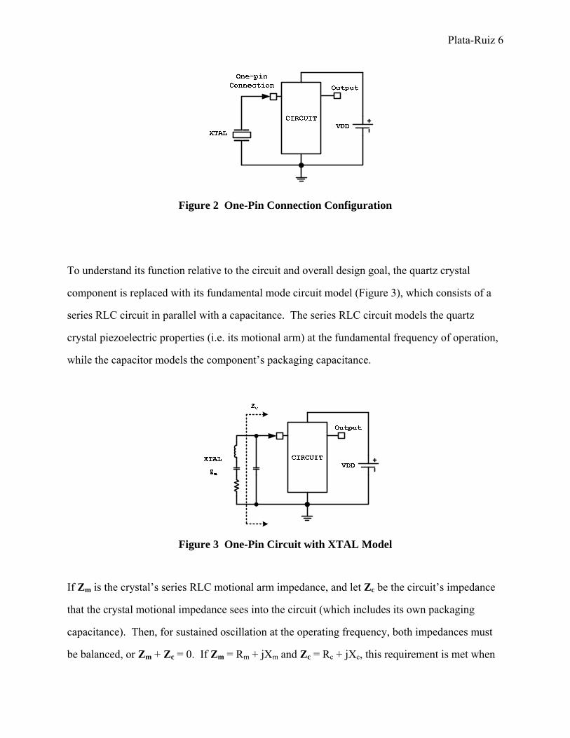
Plata-Ruiz 6
Figure 2 One-Pin Connection Configuration
To understand its function relative to the circuit and overall design goal, the quartz crystal
component is replaced with its fundamental mode circuit model (Figure 3), which consists of a
series RLC circuit in parallel with a capacitance. The series RLC circuit models the quartz
crystal piezoelectric properties (i.e. its motional arm) at the fundamental frequency of operation,
while the capacitor models the component’s packaging capacitance.
Figure 3 One-Pin Circuit with XTAL Model
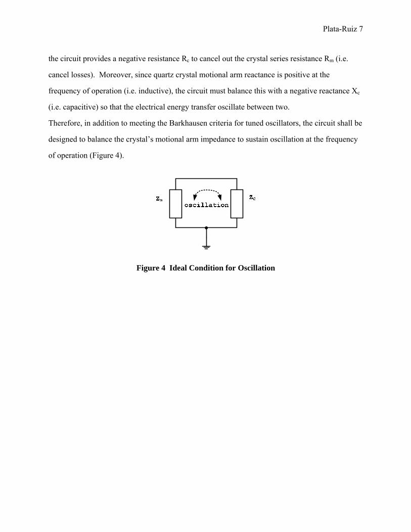
If Zm is the crystal’s series RLC motional arm impedance, and let Zc be the circuit’s impedance
that the crystal motional impedance sees into the circuit (which includes its own packaging
capacitance). Then, for sustained oscillation at the operating frequency, both impedances must
be balanced, or Zm + Zc = 0. If Zm = Rm + jXm and Zc = Rc + jXc, this requirement is met when
Plata-Ruiz 7
the circuit provides a negative resistance Rc to cancel out the crystal series resistance Rm (i.e.
cancel losses). Moreover, since quartz crystal motional arm reactance is positive at the
frequency of operation (i.e. inductive), the circuit must balance this with a negative reactance Xc
(i.e. capacitive) so that the electrical energy transfer oscillate between two.
Therefore, in addition to meeting the Barkhausen criteria for tuned oscillators, the circuit shall be
designed to balance the crystal’s motional arm impedance to sustain oscillation at the frequency
of operation (Figure 4).
Figure 4 Ideal Condition for Oscillation
Plata-Ruiz 8
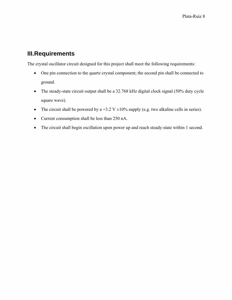
III. Requirements
The crystal oscillator circuit designed for this project shall meet the following requirements:
One pin connection to the quartz crystal component; the second pin shall be connected to
ground.
The steady-state circuit output shall be a 32.768 kHz digital clock signal (50% duty cycle
square wave).
The circuit shall be powered by a +3.2 V ±10% supply (e.g. two alkaline cells in series).
Current consumption shall be less than 250 nA.
The circuit shall begin oscillation upon power up and reach steady-state within 1 second.
Plata-Ruiz 9
IV. Design
A. Crystal Oscillator System
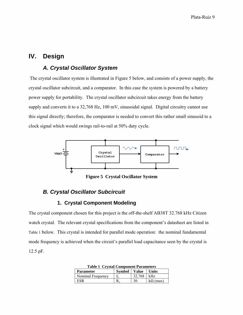
The crystal oscillator system is illustrated in Figure 5 below, and consists of a power supply, the
crystal oscillator subcircuit, and a comparator. In this case the system is powered by a battery
power supply for portability. The crystal oscillator subcircuit takes energy from the battery
supply and converts it to a 32,768 Hz, 100 mV, sinusoidal signal. Digital circuitry cannot use
this signal directly; therefore, the comparator is needed to convert this rather small sinusoid to a
clock signal which would swings rail-to-rail at 50% duty cycle.
Figure 5 Crystal Oscillator System
B. Crystal Oscillator Subcircuit
1. Crystal Component Modeling
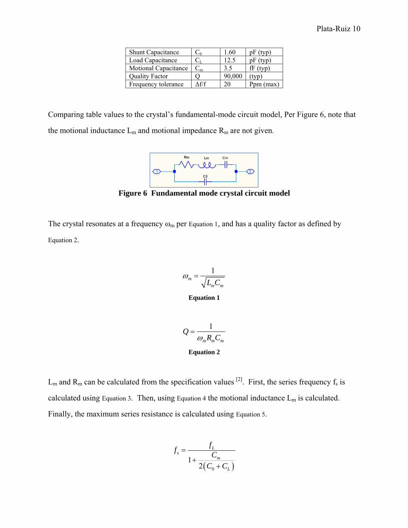
The crystal component chosen for this project is the off-the-shelf AB38T 32.768 kHz Citizen
watch crystal. The relevant crystal specifications from the component’s datasheet are listed in
Table 1 below. This crystal is intended for parallel mode operation: the nominal fundamental
mode frequency is achieved when the circuit’s parallel load capacitance seen by the crystal is
12.5 pF.
Table 1 Crystal Component Parameters
Parameter Symbol Value Units Nominal Frequency fL 32.768 kHz ESR Rs 30 kΩ (max)
Crystal Oscillator
ComparatorVBAT
Plata-Ruiz 10
Shunt Capacitance C0 1.60 pF (typ) Load Capacitance CL 12.5 pF (typ) Motional Capacitance Cm 3.5 fF (typ) Quality Factor Q 90,000 (typ) Frequency tolerance Δf/f 20 Ppm (max)
Comparing table values to the crystal’s fundamental-mode circuit model, Per Figure 6, note that
the motional inductance Lm and motional impedance Rm are not given.
Figure 6 Fundamental mode crystal circuit model
The crystal resonates at a frequency ωm per Equation 1, and has a quality factor as defined by
Equation 2.
1m
m mL C
Equation 1
1
m m m
QR C
Equation 2
Lm and Rm can be calculated from the specification values [2]. First, the series frequency fs is
calculated using Equation 3. Then, using Equation 4 the motional inductance Lm is calculated.
Finally, the maximum series resistance is calculated using Equation 5.
0
12
Ls
m
L
ff
C
C C
Plata-Ruiz 11
Equation 3
2
1 1
(2 )2s m
m sm m
f LC fL C
Equation 4
minmin min
1 1 1
2mCm m Cm s m
Q RX R X Q f C Q
Equation 5
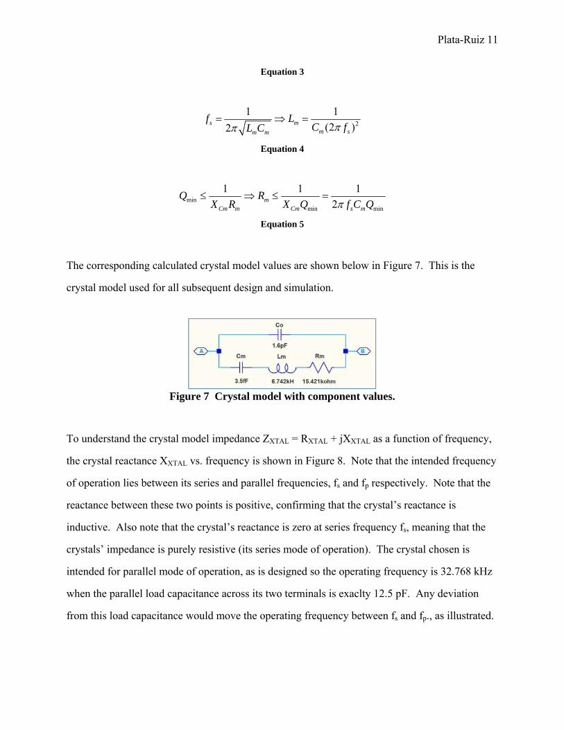
The corresponding calculated crystal model values are shown below in Figure 7. This is the
crystal model used for all subsequent design and simulation.
Figure 7 Crystal model with component values.
To understand the crystal model impedance ZXTAL = RXTAL + jXXTAL as a function of frequency,
the crystal reactance XXTAL vs. frequency is shown in Figure 8. Note that the intended frequency
of operation lies between its series and parallel frequencies, fs and fp respectively. Note that the
reactance between these two points is positive, confirming that the crystal’s reactance is
inductive. Also note that the crystal’s reactance is zero at series frequency fs, meaning that the
crystals’ impedance is purely resistive (its series mode of operation). The crystal chosen is
intended for parallel mode of operation, as is designed so the operating frequency is 32.768 kHz
when the parallel load capacitance across its two terminals is exaclty 12.5 pF. Any deviation
from this load capacitance would move the operating frequency between fs and fp., as illustrated.
Plata-Ruiz 12
Figure 8 Simulation of crystal model between series and parallel frequencies.
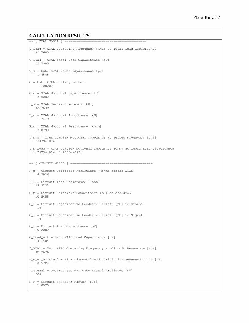
Table 2 below summarizes all the calculated model parameters for the AB38T 32.768 kHz Citizen
watch crystal.
Table 2 Calculated crystal model parameters.
Parameter Symbol Test Condition Min Typ / Est (±10%) Max Units
Frequency fL CL = 12.5pF - 32.768 - kHz
Frequency Tolerance Δf/f - - - 25 ±PPM
Quality Factor Q - 90,000 100,000 - -
Series Resistance Rs - - 27.3 30.0 kΩ
Motional Capacitance Cm - - 3.5 - fF
Shunt Capacitance C0 - - 1.5 1.6 pF
Load Capacitance CL - - 12.5 - pF
Series Frequency fs - - 32.764 - kHz
Frequency Pull Δf/f - - 125 - PPM
Motional Inductance Lm - - 6.742 - kH
Motional Resistance Rm - - 13.879 15.421 kΩ
2. Crystal Oscillator Circuit Configuration
The CMOS one-pin crystal oscillator crystal oscillator design by Ali Zadeh [1], was intended for a
standard p-well CMOS process, in which the power supply rail is negative. Ignoring the biasing
Plata-Ruiz 13
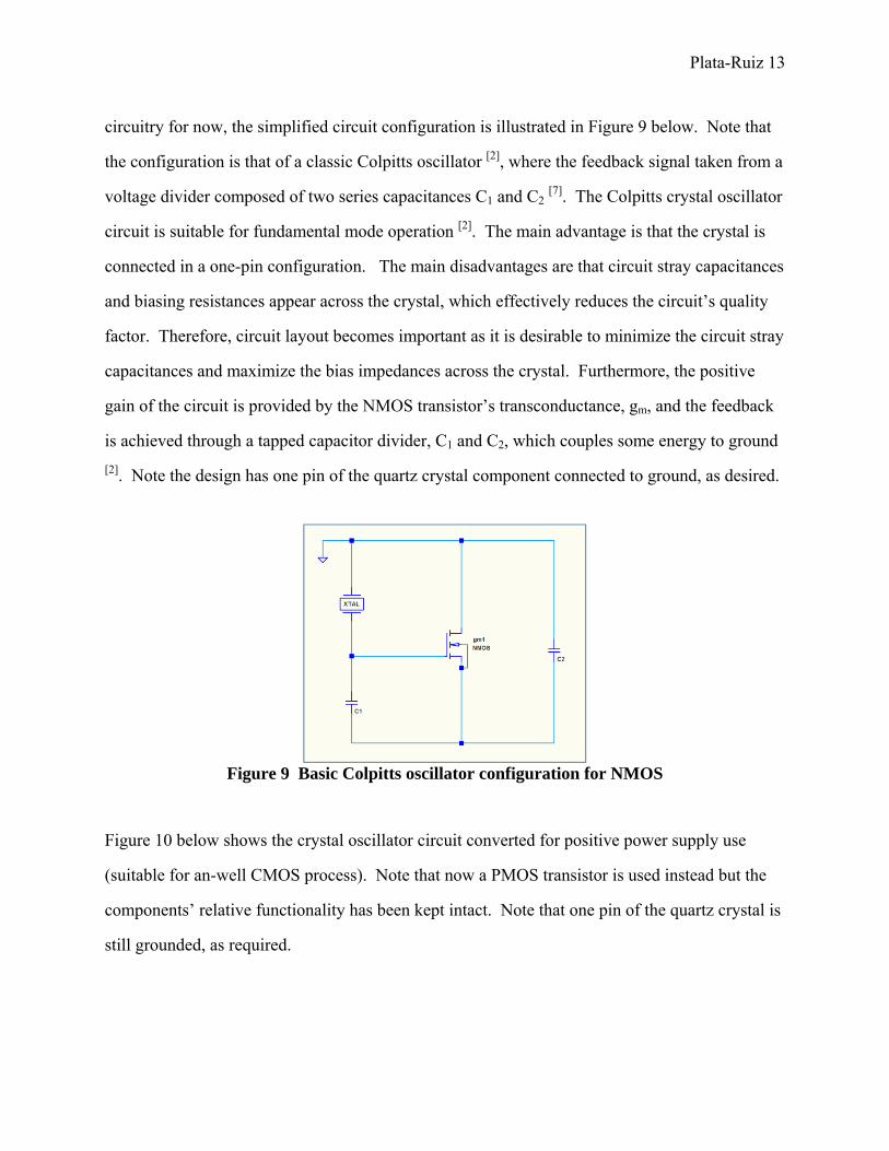
circuitry for now, the simplified circuit configuration is illustrated in Figure 9 below. Note that
the configuration is that of a classic Colpitts oscillator [2], where the feedback signal taken from a
voltage divider composed of two series capacitances C1 and C2 [7]. The Colpitts crystal oscillator
circuit is suitable for fundamental mode operation [2]. The main advantage is that the crystal is
connected in a one-pin configuration. The main disadvantages are that circuit stray capacitances
and biasing resistances appear across the crystal, which effectively reduces the circuit’s quality
factor. Therefore, circuit layout becomes important as it is desirable to minimize the circuit stray
capacitances and maximize the bias impedances across the crystal. Furthermore, the positive
gain of the circuit is provided by the NMOS transistor’s transconductance, gm, and the feedback
is achieved through a tapped capacitor divider, C1 and C2, which couples some energy to ground
[2]. Note the design has one pin of the quartz crystal component connected to ground, as desired.
Figure 9 Basic Colpitts oscillator configuration for NMOS
Figure 10 below shows the crystal oscillator circuit converted for positive power supply use
(suitable for an-well CMOS process). Note that now a PMOS transistor is used instead but the
components’ relative functionality has been kept intact. Note that one pin of the quartz crystal is
still grounded, as required.
Plata-Ruiz 14
Figure 10 Basic Colpitts oscillator configuration for PMOS
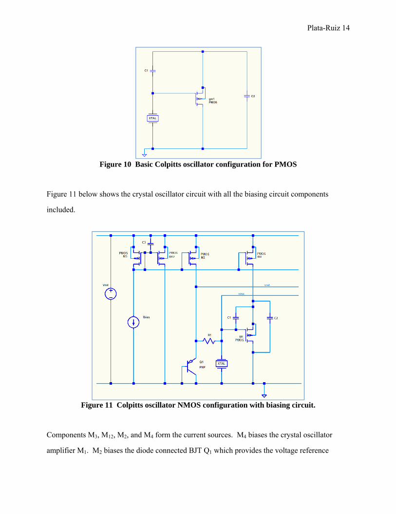
Figure 11 below shows the crystal oscillator circuit with all the biasing circuit components
included.
Figure 11 Colpitts oscillator NMOS configuration with biasing circuit.
Components M3, M12, M2, and M4 form the current sources. M4 biases the crystal oscillator
amplifier M1. M2 biases the diode connected BJT Q1 which provides the voltage reference
Plata-Ruiz 15
(about 0.5 V) for the gate of M1 through the protection resistor R1. The W/L ratio of the current
source transistors need to be adjusted to scale the proper level of Ibias needed to bias the
corresponding component. M12 is used as dummy current source to externally monitor the
biasing current through M1. Therefore, M12 would have to be matched to M4. The oscillation
signal is sampled across R1. This is the output of the crystal oscillator subcircuit.
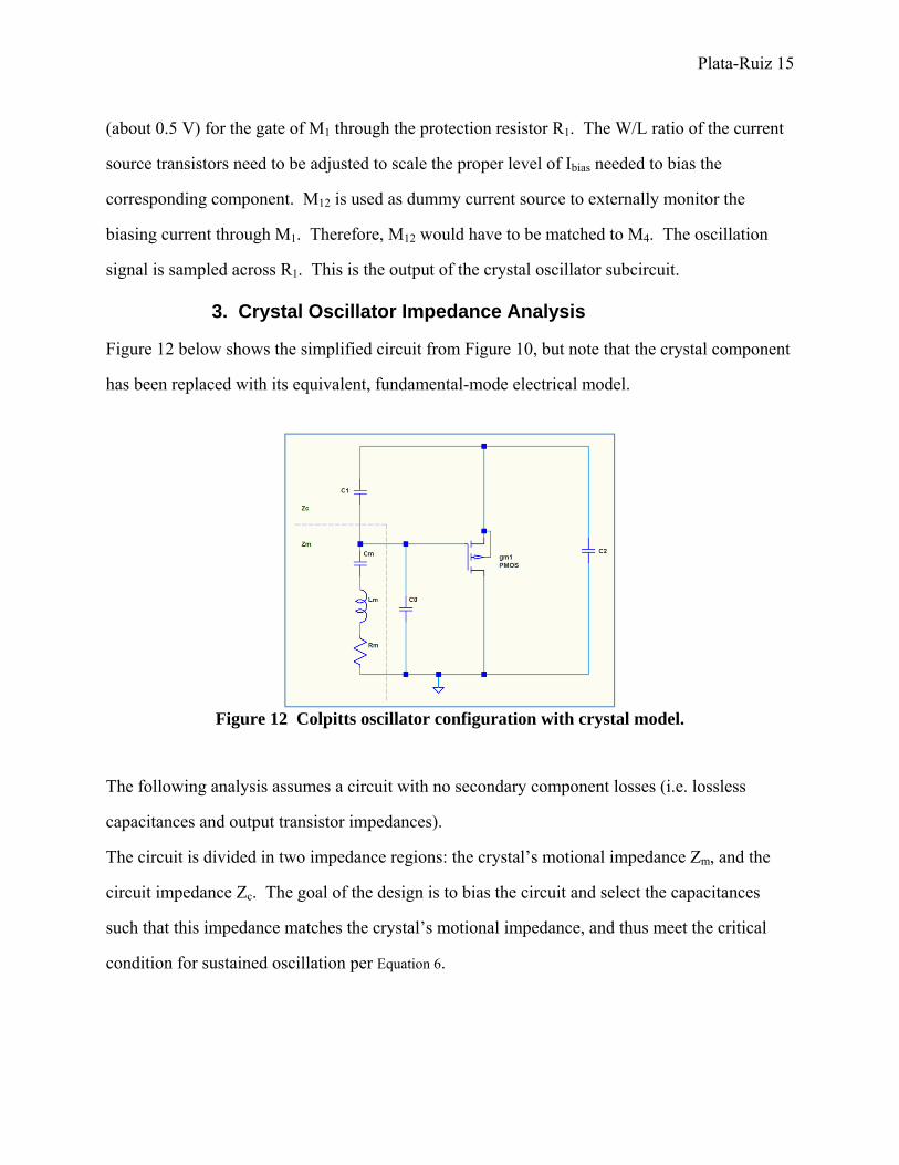
3. Crystal Oscillator Impedance Analysis
Figure 12 below shows the simplified circuit from Figure 10, but note that the crystal component
has been replaced with its equivalent, fundamental-mode electrical model.
Figure 12 Colpitts oscillator configuration with crystal model.
The following analysis assumes a circuit with no secondary component losses (i.e. lossless
capacitances and output transistor impedances).
The circuit is divided in two impedance regions: the crystal’s motional impedance Zm, and the
circuit impedance Zc. The goal of the design is to bias the circuit and select the capacitances
such that this impedance matches the crystal’s motional impedance, and thus meet the critical
condition for sustained oscillation per Equation 6.
Plata-Ruiz 16
0C mZ Z
Equation 6
The motional impedance of the crystal is given by Equation 7. Due to the crystal’s high Q, the
crystal’s operating frequency ω is usually very close to the resonant frequency ωm, and this
difference is defined as the frequency pull, or Δω [1]. Therefore, Equation 7 can be approximated
by Equation 8 as a function of the frequency pull of the design.
m m mm
jZ R j L
C
Equation 7
2
2m m
m
Z R jC
Equation 8
On the circuit’s side, the circuit’s impedance Zc can be broken down by its real and imaginary
parts, per Equation 9.
Re ImC C CZ Z j Z
Equation 9
Therefore, the sustained oscillation condition (Equation 6) is met when:
Re 0m cR Z
Equation 10
2
2Im c
m
ZC
Equation 11
Plata-Ruiz 17
According to Ali Zadeh, if –ReRc > Rm , the frequency of amplitude increases until it is
limited by circuit nonlinear effects, at which distortion my occur.
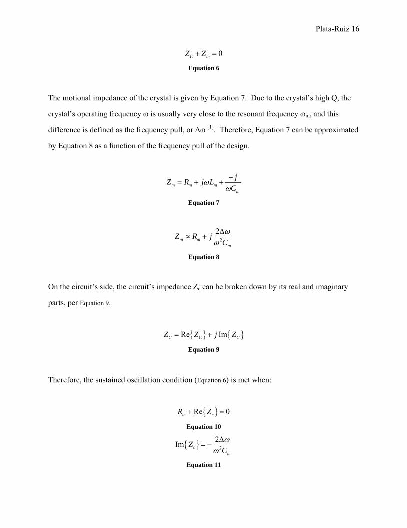
Figure 13 shows the updated simplified oscillator circuit with a parallel capacitance Cp across the
crystal motional impedance. This capacitance models both the crystal’s shunt capacitance C0,
and any other parallel stray capacitance introduced by the circuit’s layout.
Figure 13 Colpitts oscillator with crystal model and circuit transconductance.
Referencing the circuit from Figure 13, the real part of Equation 9 is given by Equation 12 and the
imaginary part is given by Equation 13.
1 22 2 2
1 2 2 1
Re( )
mC
m p p p
g C CZ
g C C C C C C C
Equation 12
2 21 2 1 2 2 1
2 2 21 2 2 1
( )Im
( )
m p p pC
m p p p
g C C C C C C C C CZ
g C C C C C C C
Equation 13
Plata-Ruiz 18
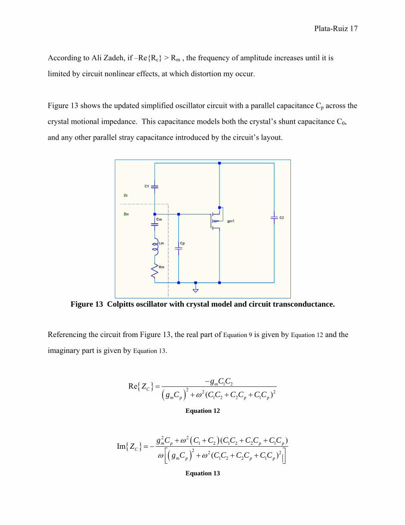
Table 3 below shows all the calculated values for the ideal lossless circuit design values using the
impedance analysis approach just presented [1].
Table 3 Calculated crystal impedances ideal circuit impedances.
Parameter Symbol Typ Units
XTAL Impedance Zm 13.879+348.080j kΩ
Desired Circuit Impedance Zc -13.879-348.080j kΩ
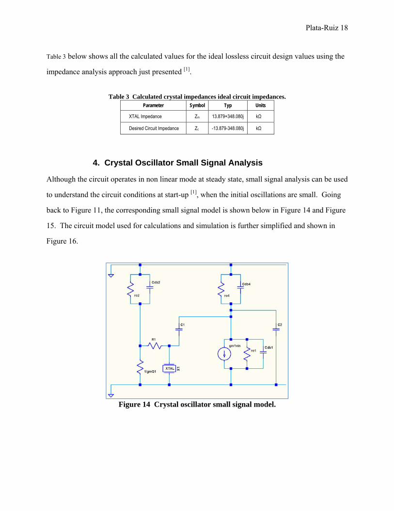
4. Crystal Oscillator Small Signal Analysis
Although the circuit operates in non linear mode at steady state, small signal analysis can be used
to understand the circuit conditions at start-up [1], when the initial oscillations are small. Going
back to Figure 11, the corresponding small signal model is shown below in Figure 14 and Figure
15. The circuit model used for calculations and simulation is further simplified and shown in
Figure 16.
Figure 14 Crystal oscillator small signal model.
Plata-Ruiz 19
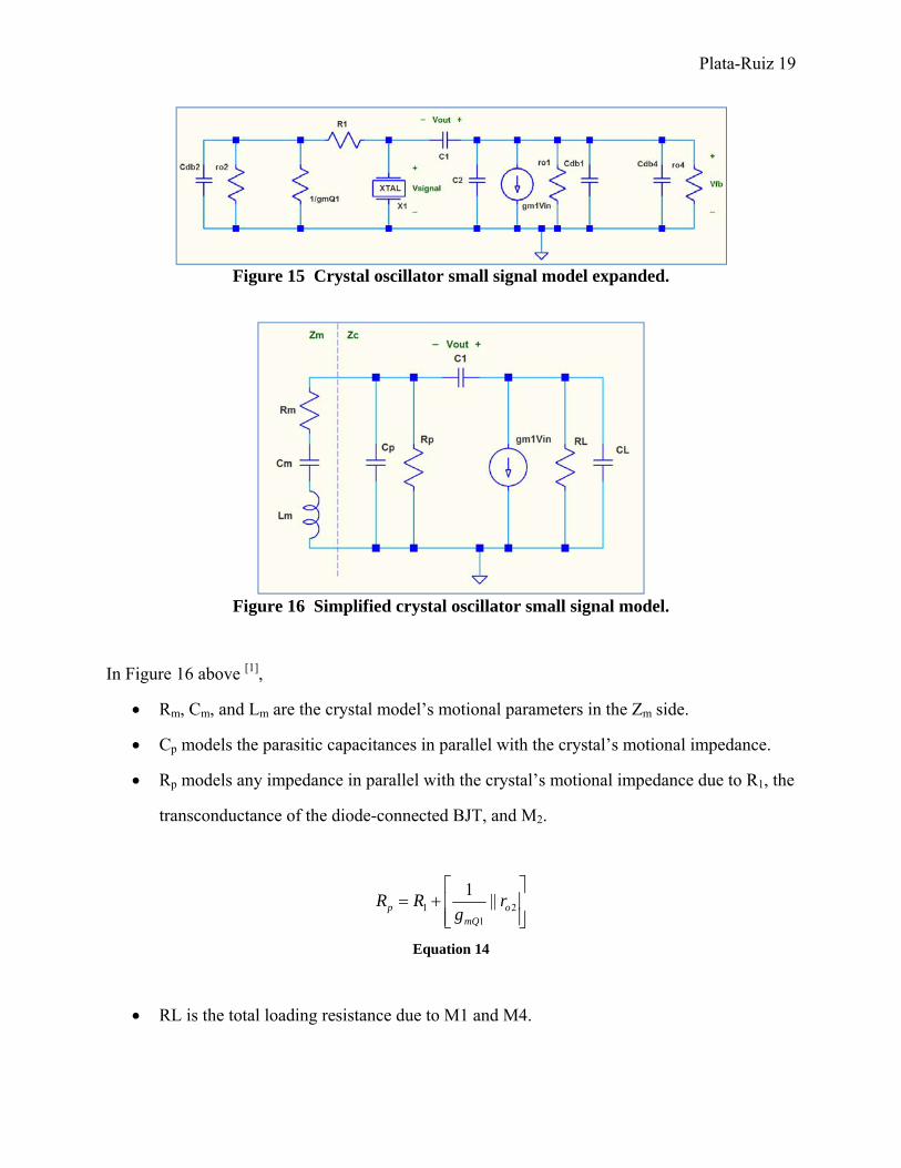
Figure 15 Crystal oscillator small signal model expanded.
Figure 16 Simplified crystal oscillator small signal model.
In Figure 16 above [1],
Rm, Cm, and Lm are the crystal model’s motional parameters in the Zm side.
Cp models the parasitic capacitances in parallel with the crystal’s motional impedance.
Rp models any impedance in parallel with the crystal’s motional impedance due to R1, the
transconductance of the diode-connected BJT, and M2.
1 21
1||p o
mQ
R R rg
Equation 14
RL is the total loading resistance due to M1 and M4.
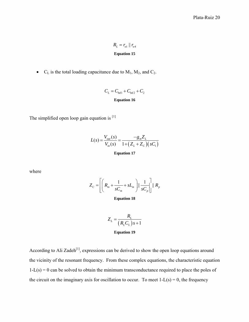
Plata-Ruiz 20
1 4||L o oR r r Equation 15
CL is the total loading capacitance due to M1, M2, and C2.
1 2 2L bd bdC C C C Equation 16
The simplified open loop gain equation is [1]
1
( )( )
( ) 1out m L
in L C
V s g ZL s
V s Z Z sC
Equation 17
where
1 1|| ||C m m p
m p
Z R sL RsC sC
Equation 18
1L
LL L
RZ
R C s
Equation 19
According to Ali Zadeh[1], expressions can be derived to show the open loop equations around
the vicinity of the resonant frequency. From these complex equations, the characteristic equation
1-L(s) = 0 can be solved to obtain the minimum transconductance required to place the poles of
the circuit on the imaginary axis for oscillation to occur. To meet 1-L(s) = 0, the frequency
Plata-Ruiz 21
pulling is given by Equation 20 and the critical transconductance is given by Equation 21. The
relative frequency pulling can be reduced by increasing the capacitances, but the current
consumption will be increased [1]. Also, it is recommended to decrease gmin(critical) at a given
frequency, decrease Rm and Cp, while making C1 = C2.
1
1 1
11
2m L
mL p L p
C C C
C C C C C C
Equation 20
221 1
min( )1
m L p L p
criticalL
R C C C C C Cg
C C
Equation 21
Assuming Ibias = 20nA and C1 = C2 = 10 pF, Table 4 below summarizes the calculations for the
method presented in this section.
Table 4 Calculated small signal model parameters.
Parameter Symbol Typ Units
Parasitic Resistance Rp 6.293 MΩ
Load Resistance RL 83.3 TΩ
Load Capacitance CL 10.2 pF
Parasitic Capacitance Cp 10.5 pF
M1 Fundamental Mode Critical Transconductance
gm(critical) 0.572 µS
Operating Frequency f 32.768 µS
5. Crystal Oscillator Large Signal Analysis
The crystal oscillator generates a signal that initially increases due to positive feedback and then
it gets limited to certain amplitude by non linear effects. At the operating frequency, if 1-
L(s) = 0, the poles are at the the imaginary axis, and the circuit meets the Barkhausen criteria.
Plata-Ruiz 22
At this point in steady state, the transconductance of the amplifier M1 equals the minimum
transconductance. Equation 25 through Equation 25 allow to estimate the M1 dc transconductance in
the weak inversion region [1]. Note that I0 and I1 in Equation 25 are modified Bessel functions of
the first kind, of order 0 and 1, respectively [1].
( ) 0
( ) 12m dc
m critical
g I
g I
Equation 22
1signalF
F T
VN
N nV
Equation 23
LF
m
CN
C
Equation 24
( )( )
s dcm dc
T
Ig
nV
Equation 25
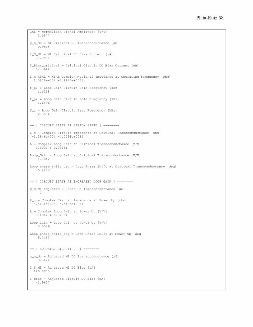
Table 5 below summarizes all the calculations for the crystal oscillator circuit when the
Barkhausen criterion has been met at a minimum (Loop Gain = 1, Loop Phase Shift = 0°).
Table 5 Calculated large signal crystal model parameters.
Parameter Symbol Typ Units
Boltzmann constant k 13.807E-24 JK-1
Temperature (room) T 300 K
Electron Charge q 160.218E-21 C
Thermal Voltage VT 25.85 mV
Transistor Slope Factor n 1.5 -
Plata-Ruiz 23
Desired Amplitude Vsignal 250.0 mV
Feedback Factor NF 1.007 -
Normalized Amplitude χ 2.588 -
DC to Critical Transconductance
gm(DC) /gm(critical)
5.840 -
Critical Transconductance gm(critical) 0.572 µS
DC Transconductance gm(DC) 0.957 µS
M1 DC Bias current Is(DC) 37 nA
DC Total Bias current Is(DC) 12 nA
C. Computer Simulation
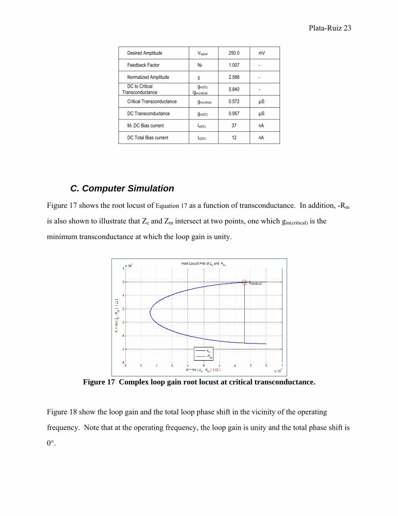
Figure 17 shows the root locust of Equation 17 as a function of transconductance. In addition, -Rm
is also shown to illustrate that Zc and Zm intersect at two points, one which gm(critical) is the
minimum transconductance at which the loop gain is unity.
Figure 17 Complex loop gain root locust at critical transconductance.
Figure 18 show the loop gain and the total loop phase shift in the vicinity of the operating
frequency. Note that at the operating frequency, the loop gain is unity and the total phase shift is
0°.
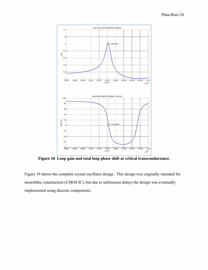
Plata-Ruiz 24
Figure 18 Loop gain and total loop phase shift at critical transconductance.
Figure 19 shows the complete crystal oscillator design. This design was originally intended for
monolithic construction (CMOS IC), but due to unforeseen delays the design was eventually
implemented using discrete components.
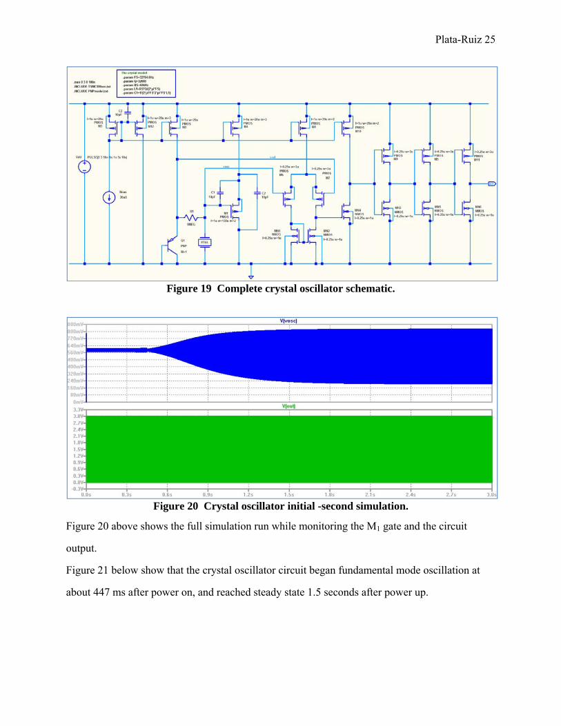
Plata-Ruiz 25
Figure 19 Complete crystal oscillator schematic.
Figure 20 Crystal oscillator initial -second simulation.
Figure 20 above shows the full simulation run while monitoring the M1 gate and the circuit
output.
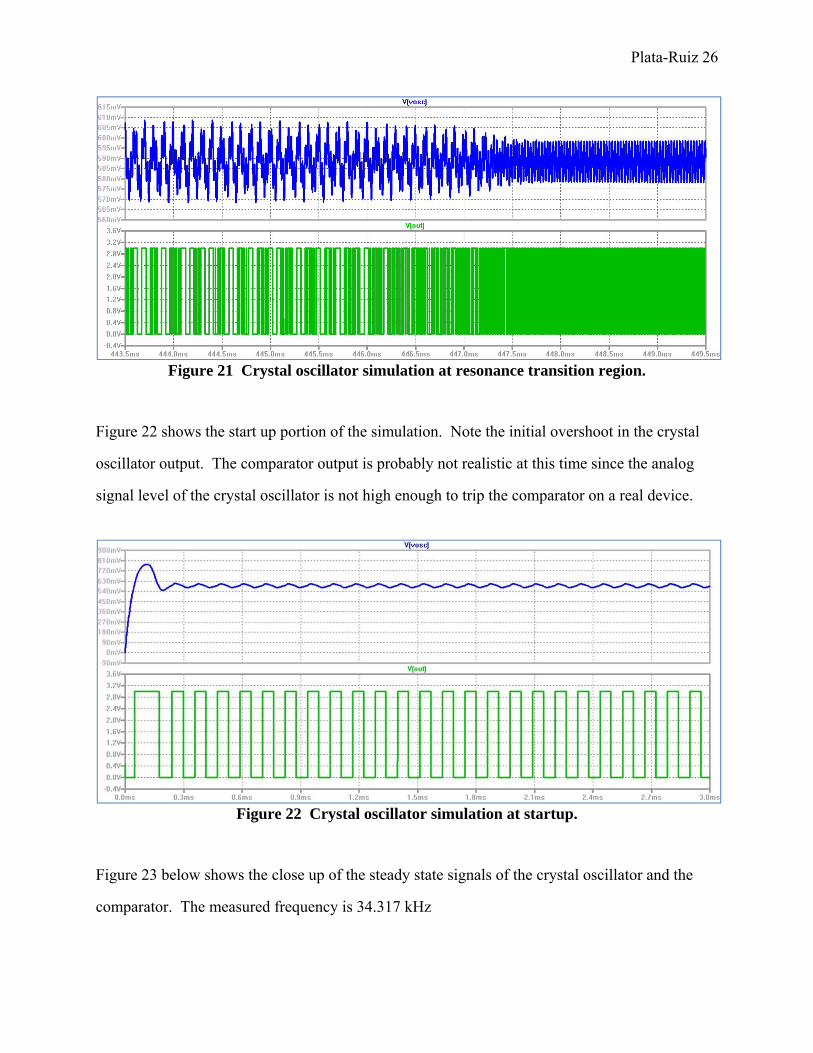
Figure 21 below show that the crystal oscillator circuit began fundamental mode oscillation at
about 447 ms after power on, and reached steady state 1.5 seconds after power up.
Plata-Ruiz 26
Figure 21 Crystal oscillator simulation at resonance transition region.
Figure 22 shows the start up portion of the simulation. Note the initial overshoot in the crystal
oscillator output. The comparator output is probably not realistic at this time since the analog
signal level of the crystal oscillator is not high enough to trip the comparator on a real device.
Figure 22 Crystal oscillator simulation at startup.
Figure 23 below shows the close up of the steady state signals of the crystal oscillator and the
comparator. The measured frequency is 34.317 kHz
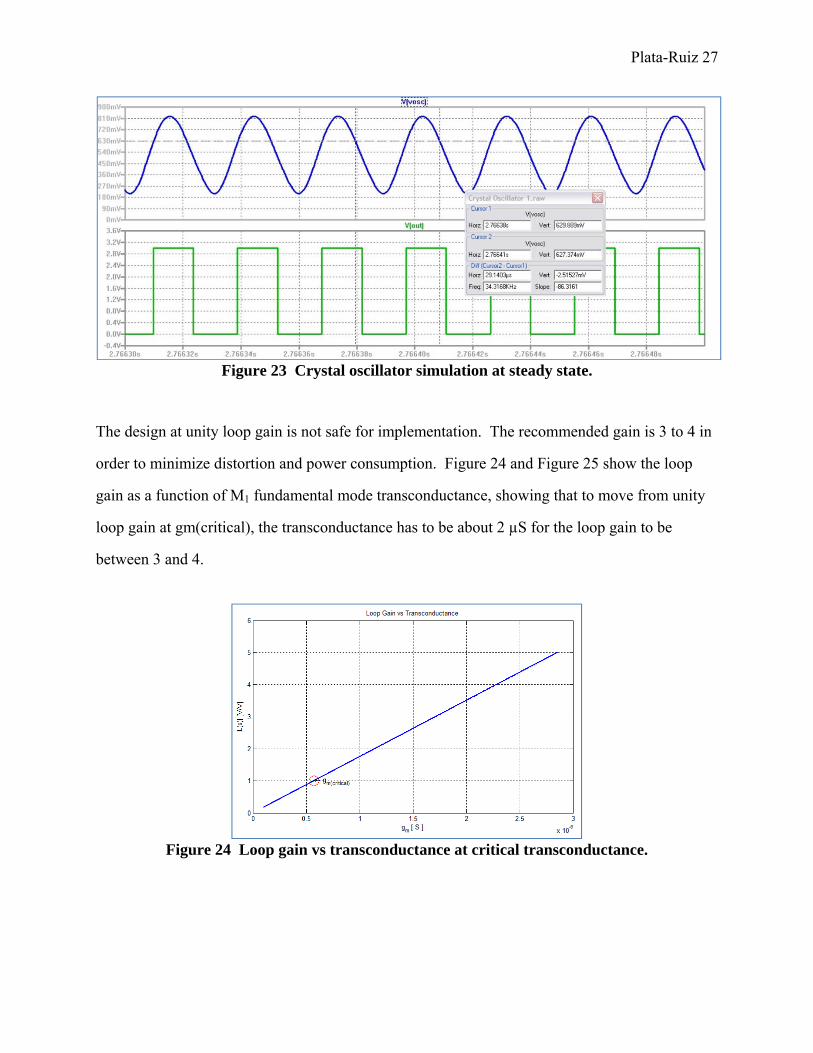
Plata-Ruiz 27
Figure 23 Crystal oscillator simulation at steady state.
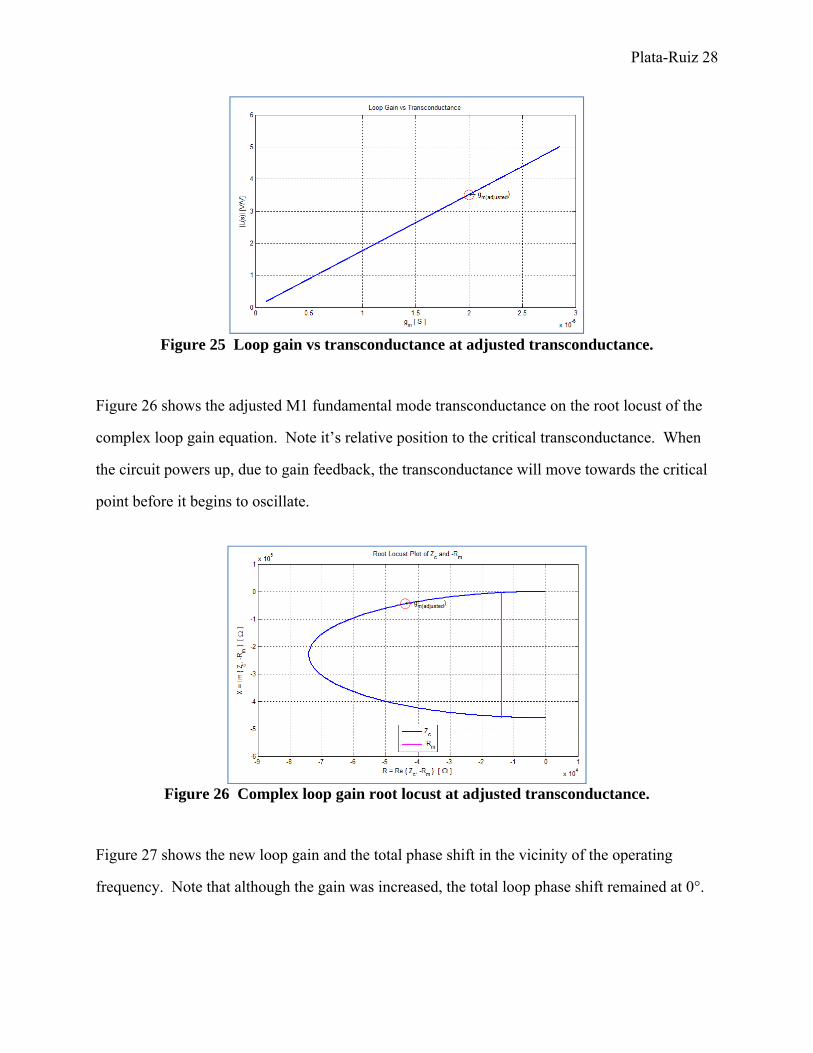
The design at unity loop gain is not safe for implementation. The recommended gain is 3 to 4 in
order to minimize distortion and power consumption. Figure 24 and Figure 25 show the loop
gain as a function of M1 fundamental mode transconductance, showing that to move from unity
loop gain at gm(critical), the transconductance has to be about 2 µS for the loop gain to be
between 3 and 4.
Figure 24 Loop gain vs transconductance at critical transconductance.
Plata-Ruiz 28
Figure 25 Loop gain vs transconductance at adjusted transconductance.
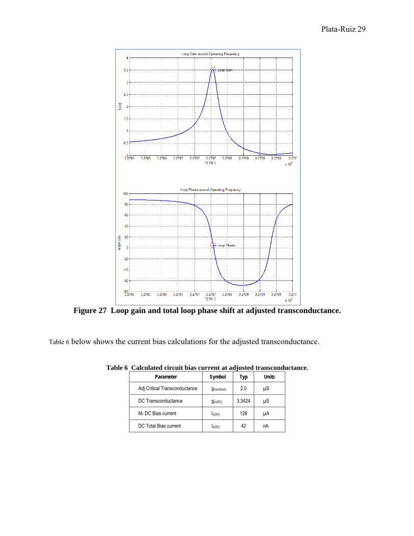
Figure 26 shows the adjusted M1 fundamental mode transconductance on the root locust of the
complex loop gain equation. Note it’s relative position to the critical transconductance. When
the circuit powers up, due to gain feedback, the transconductance will move towards the critical
point before it begins to oscillate.
Figure 26 Complex loop gain root locust at adjusted transconductance.
Figure 27 shows the new loop gain and the total phase shift in the vicinity of the operating
frequency. Note that although the gain was increased, the total loop phase shift remained at 0°.
Plata-Ruiz 29
Figure 27 Loop gain and total loop phase shift at adjusted transconductance.
Table 6 below shows the current bias calculations for the adjusted transconductance.
Table 6 Calculated circuit bias current at adjusted transconductance.
Parameter Symbol Typ Units
Adj Critical Transconductance gm(critical) 2.0 µS
DC Transconductance gm(DC) 3.3424 µS
M1 DC Bias current Is(DC) 126 µA
DC Total Bias current Is(DC) 42 nA

Plata-Ruiz 30
V. Test Plan
The circuit shall be tested for design verification.
Power Up: Verify that the device under test (DUT) runs every time after power up.
Frequency: Verify that the frequency is 32.768 kHz ± 20 PPM.
Duty Cycle: Verify that the duty cycle is 50%.
Time to Steady State: Verify that the time to steady state is within 1 seconds.
The circuit shall be tested for design characterization.
Minimum bias current: use an SMU to determine the minimum bias current that
would start up the oscillations. Start from 100 nA and decrease the current by 5 nA
until the circuit no longer starts up.
Minimum supply voltage: use a programmable power supply to determine the lowest
power level that would start up the oscillations. Start from 3.5 V and decrease the
supply voltage by 0.1 V until the circuit no longer starts up. Repeat the test while the
circuit is running to determine the minimum supply level that will sustain oscillations.
Output load: Use a pot resistance to determine the largest load that the circuit can
sustain without affecting the oscillation waveform characteristics.

Plata-Ruiz 31
VI. Development and Construction
The circuit design was originally intended for n-well CMOS IC implementation. Nevertheless,
for reasons outside of my control, it was determined that this approach was not feasible and I
decided to implement on a breadboard at the discrete level. I chose the Advanced Linear
Devices ADL11XX MOSFET series of devices, which feature matched pair/quad transistors and
I thought were suitable for the design construction. I was aware of the disadvantages of
implementing the design with discrete components from the beginning:
The geometries of the components are fixed. The detailed analysis that went into setting
the relative geometry rations is not possible with such components.
The component’s process characteristics are unknown and must be inferred from the
specification documentation.
Building a low-power circuit with discrete components on a breadboard is risky because
of the stray capacitances that plague breadboards which are probably also greater than the
circuit component values.
Nevertheless, since the best way to determine whether an idea works or not is by actually trying
it. Figure 28 shows the initial breadboard implementation.
As expected, I encountered problems running and testing the breadboarded circuit. After talking
to Dr. Dennis, he suggested I rebuild the circuit on a copper plate to minimize stray capacitances.
The rebuilt circuit is shown below in Figure 29 below.

Plata-Ruiz 32
Figure 28 Crystal oscillator circuit implemented on a breadboard.
Figure 29 Crystal oscillator circuit implemented on a copper ground plane.
Plata-Ruiz 33
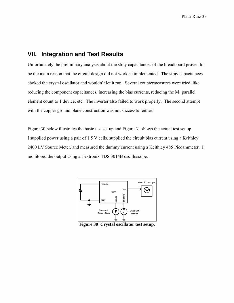
VII. Integration and Test Results
Unfortunately the preliminary analysis about the stray capacitances of the breadboard proved to
be the main reason that the circuit design did not work as implemented. The stray capacitances
choked the crystal oscillator and wouldn’t let it run. Several countermeasures were tried, like
reducing the component capacitances, increasing the bias currents, reducing the M1 parallel
element count to 1 device, etc. The inverter also failed to work properly. The second attempt
with the copper ground plane construction was not successful either.
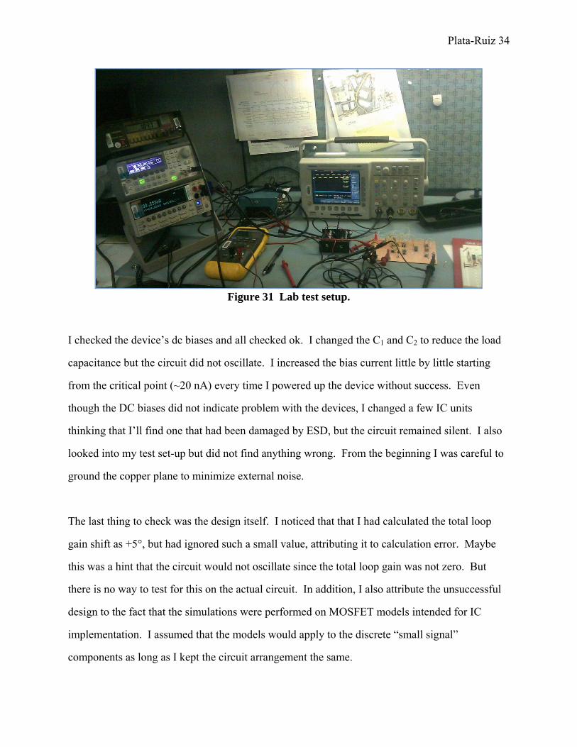
Figure 30 below illustrates the basic test set up and Figure 31 shows the actual test set up.
I supplied power using a pair of 1.5 V cells, supplied the circuit bias current using a Keithley
2400 LV Source Meter, and measured the dummy current using a Keithley 485 Picoammeter. I
monitored the output using a Tektronix TDS 3014B oscilloscope.
DUT
A
Oscilloscope
Current Meter
Current Bias Sink
VBAT+
GND
IBIAS
ISENSE
OUT
Figure 30 Crystal oscillator test setup.
Plata-Ruiz 34
Figure 31 Lab test setup.
I checked the device’s dc biases and all checked ok. I changed the C1 and C2 to reduce the load
capacitance but the circuit did not oscillate. I increased the bias current little by little starting
from the critical point (~20 nA) every time I powered up the device without success. Even
though the DC biases did not indicate problem with the devices, I changed a few IC units
thinking that I’ll find one that had been damaged by ESD, but the circuit remained silent. I also
looked into my test set-up but did not find anything wrong. From the beginning I was careful to
ground the copper plane to minimize external noise.
The last thing to check was the design itself. I noticed that that I had calculated the total loop
gain shift as +5°, but had ignored such a small value, attributing it to calculation error. Maybe
this was a hint that the circuit would not oscillate since the total loop gain was not zero. But
there is no way to test for this on the actual circuit. In addition, I also attribute the unsuccessful
design to the fact that the simulations were performed on MOSFET models intended for IC
implementation. I assumed that the models would apply to the discrete “small signal”
components as long as I kept the circuit arrangement the same.

Plata-Ruiz 35
VIII. Conclusion and Recomendations
Designing crystal oscillators is quite challenging but at the same time it is one of the best
opportunities to revisit all areas of circuit design: from integrated circuit design, to control
theory, small signal and large signal modeling circuit modeling, solid state electronics, low
power design, and many more.
Coming up with a unsuccessful design is the best learning tool for the practicing engineer, as it
first teaches humility, forces the engineer to review all steps in much more detail, and provides
for new ideas for the next attempt.
The design, simulation, and prototyping activities should be kept in agreement at all times. Any
decision in one area should be modeled in the other as to anticipate performance issue ahead of
time. Simulation is as good as the model and successful simulation does not guarantee a
successful product. Spend more time at the design stage developing the circuit model. Make
sure that the simulations agree with prototype performance. Adjust model and iterate circuit
designs.
Plata-Ruiz 36
IX. Bibliography
Works Cited
[1] Zadeh, Ali E. “A Micropower Battery-Operated One-Pin Crystal Oscillator.” Circuits and
Systems, 1993, Proceedings of the 36th Midwest Symposium on Circuits and Systems Aug.
1993: 1382–1387.
<http://ieeexplore.ieee.org/xpls/abs_all.jsp?arnumber=343363&tag=1>
[2] Bible, Steven. “Crystal Oscillator Basics and Crystal Selection for rfPICTM and
PICmicro® Devices.” Application Notes, AN826, Microchip Technology, Inc, Jan. 2002.
< http://www.microchip.com/stellent/idcplg?IdcService=SS_GET_PAGE&nodeId=1824&appnote=en011973 >
[3] Williams, Tim. The Circuit Designer’s Companion; second edition. Chichester, UK:
Elsevier Ltd, 2005.
[4] Allen, Phyllip E., Douglas R. Holberg. CMOS Analog Circuit Design. Philadelphia:
Saunders College Publishing, 1987
[5] Jaeger, Richard C. Microelectronic Circuit Design. New York: McGraw-Hill Companies,
Inc., 1997.
[6] Crystal oscillator. Wikipedia, the free encyclopedia. Wikimedia Foundation, Inc., March
2011.
< http://en.wikipedia.org/wiki/Crystal_oscillator >
[7] Colpitts oscillator. Wikipedia, the free encyclopedia. Wikimedia Foundation, Inc., March
2011.
< http://en.wikipedia.org/wiki/Colpitts_oscillator >

Plata-Ruiz 37
X. Appendices
Plata-Ruiz 38
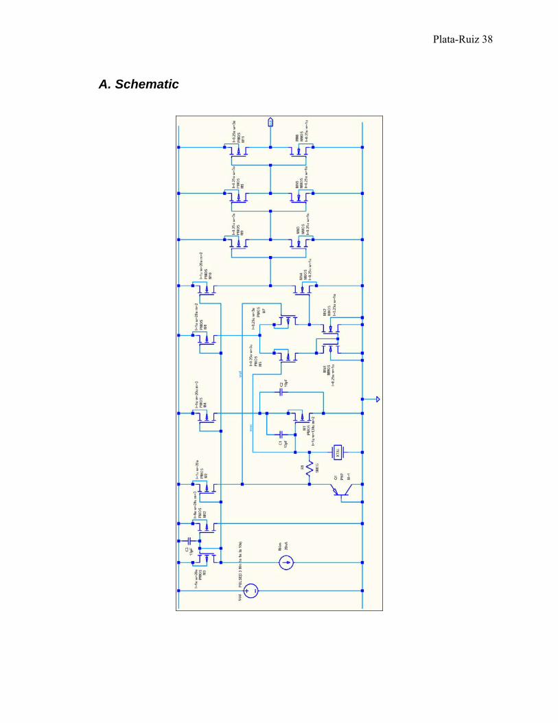
A. Schematic
Plata-Ruiz 39
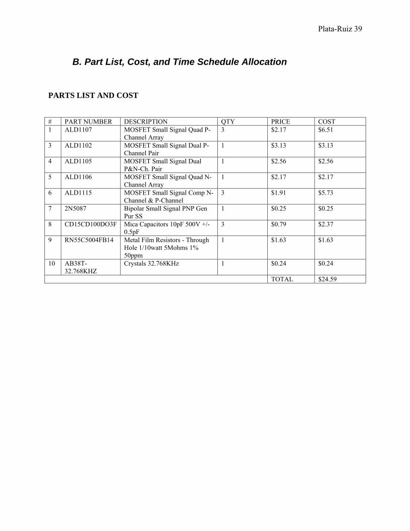
B. Part List, Cost, and Time Schedule Allocation
PARTS LIST AND COST
# PART NUMBER DESCRIPTION QTY PRICE COST 1 ALD1107 MOSFET Small Signal Quad P-
Channel Array 3 $2.17 $6.51
3 ALD1102 MOSFET Small Signal Dual P-Channel Pair
1 $3.13 $3.13
4 ALD1105 MOSFET Small Signal Dual P&N-Ch. Pair
1 $2.56 $2.56
5 ALD1106 MOSFET Small Signal Quad N-Channel Array
1 $2.17 $2.17
6 ALD1115 MOSFET Small Signal Comp N-Channel & P-Channel
3 $1.91 $5.73
7 2N5087 Bipolar Small Signal PNP Gen Pur SS
1 $0.25 $0.25
8 CD15CD100DO3F Mica Capacitors 10pF 500V +/-0.5pF
3 $0.79 $2.37
9 RN55C5004FB14 Metal Film Resistors - Through Hole 1/10watt 5Mohms 1% 50ppm
1 $1.63 $1.63
10 AB38T-32.768KHZ
Crystals 32.768KHz 1 $0.24 $0.24
TOTAL $24.59
Plata-Ruiz 40
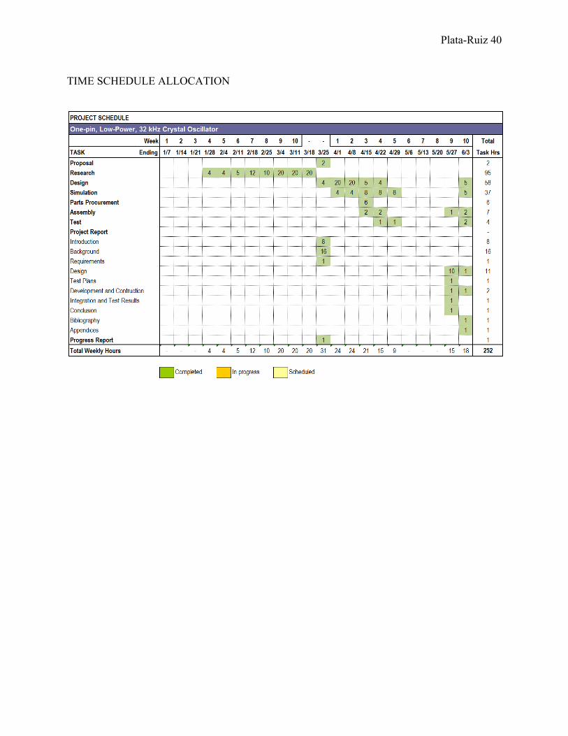
TIME SCHEDULE ALLOCATION
Plata-Ruiz 41
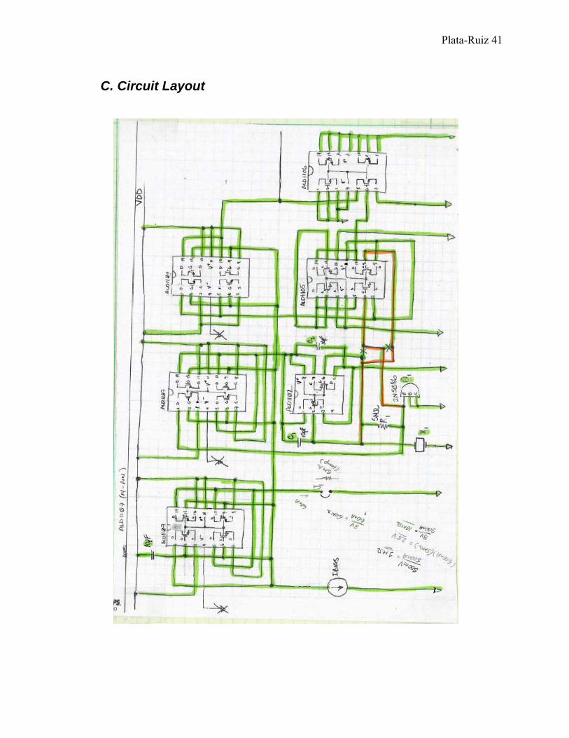
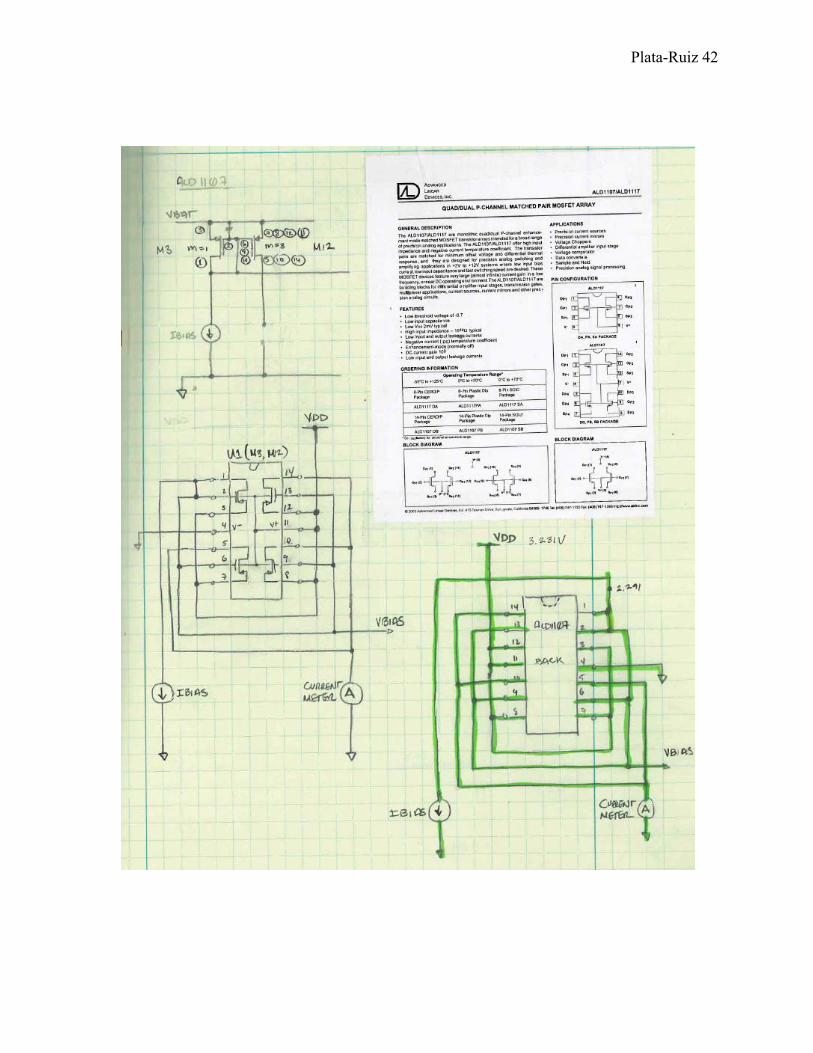
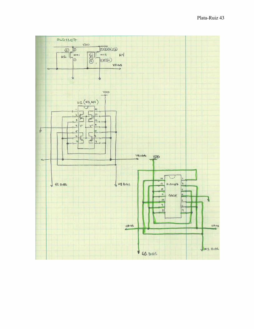
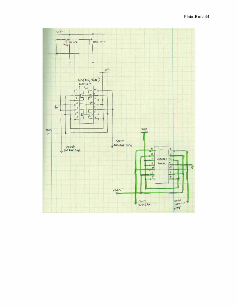
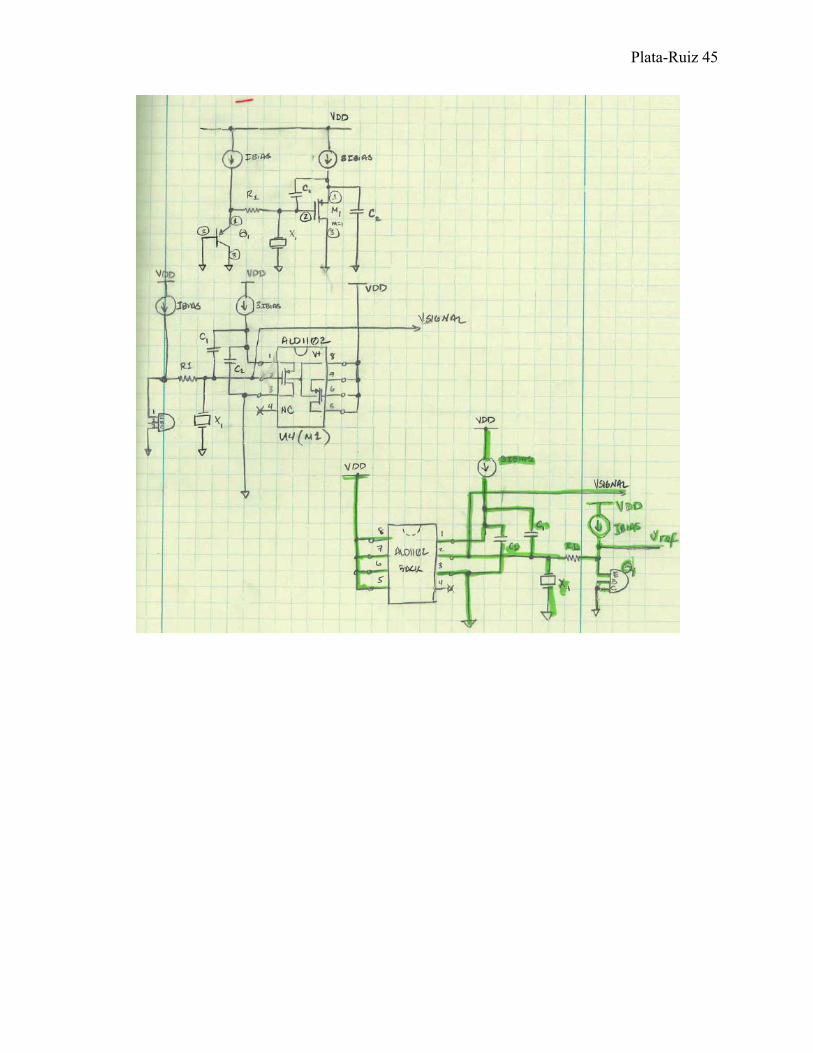
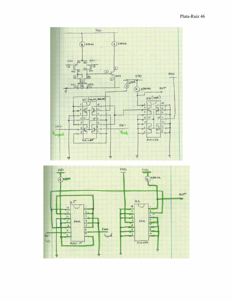
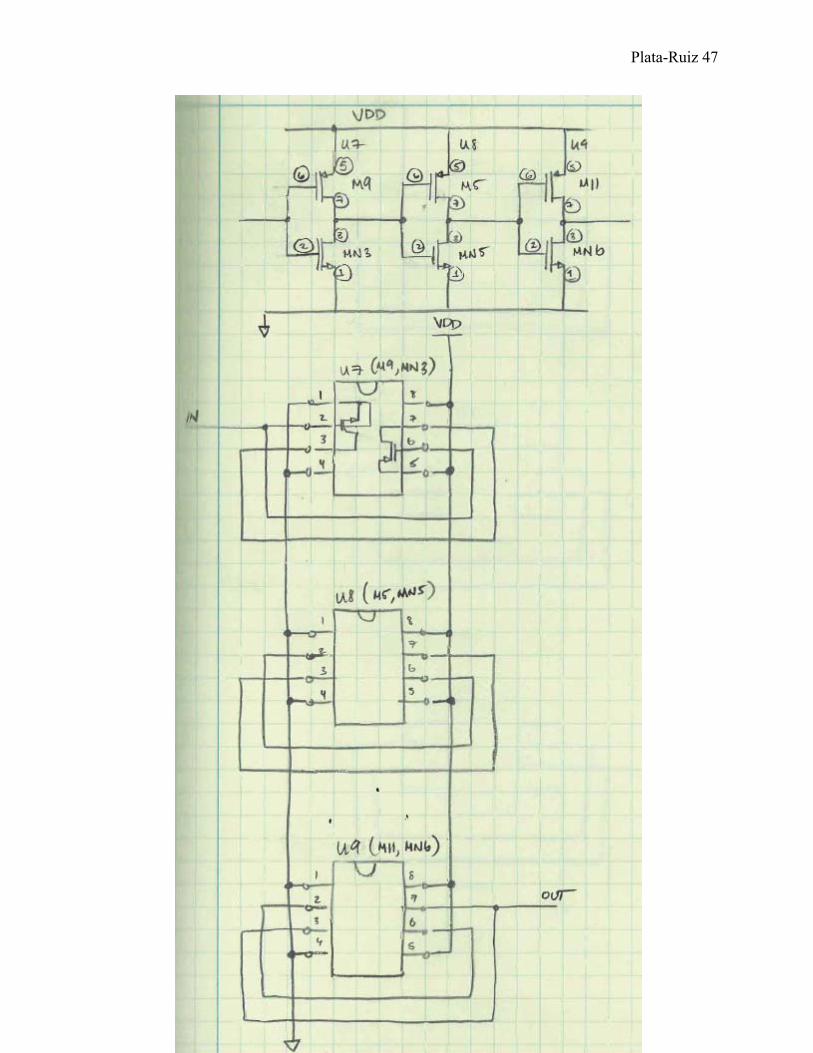
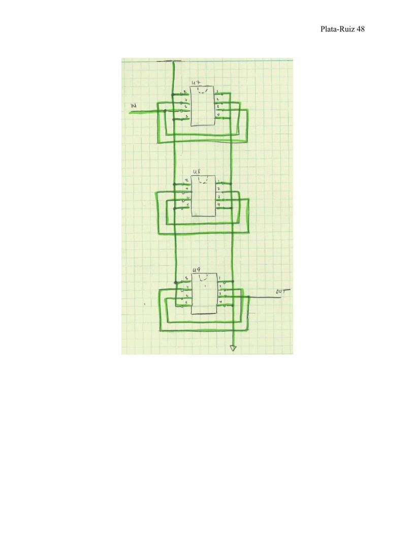
C. Circuit Layout
Plata-Ruiz 42
Plata-Ruiz 43
Plata-Ruiz 44
Plata-Ruiz 45
Plata-Ruiz 46
Plata-Ruiz 47
Plata-Ruiz 48
Plata-Ruiz 49
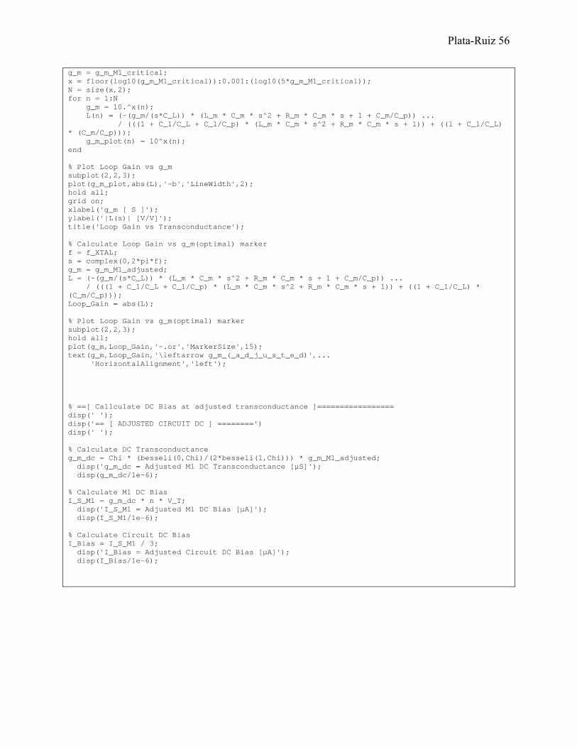
D. Program Listing
MATLAB PROGRAM FOR CALCULATIONS AND ROOT LOCUST ANALYSIS % CRYSTAL OSCILLATOR DESIGN CALCULATIONS % AARON PLATA_RUIZ % CAL POLY SENIOR PROJECT (SPRING 2011) clear clc % SMALL SIGNAL ANALYSIS % ==[ XTAL MODEL ]============================ disp('== [ XTAL MODEL ] ==========================================') disp(' '); f_Load = 32768; % [Hz] Nominal Operational Frequency @ C_Load = 12.5 pF disp('f_Load = XTAL Operating Frequency [kHz] at ideal Load Capacitance'); disp(f_Load/1e3); C_Load = 12.5e-12; %[F] Nominal Load Capacitance disp('C_Load = XTAL ideal Load Capacitance [pF]'); disp(C_Load/1e-12); C_0_max = 1.6e-12; % [F] Maximum Shunt Capacitance C_0 = C_0_max / (1 + 0.10); % [F] Estimated Shunt Capacitance disp('C_0 = Est. XTAL Shunt Capacitance [pF]'); disp(C_0/1e-12); f_Tol = 25; % [ppm] Frequency Tolerance (DF/F) Q_min = 90000; % Minimum Quality Factor Q = Q_min / (1 - 0.10); % Estimated Nominal Quality Factor disp('Q = Est. XTAL Quality Factor'); disp(Q); R_ESR_max = 30000; % [Ohm] Maximum Series Resistance R_ESR = R_ESR_max / (1 + 0.10); % [Ohm] Estimated Series Resistance C_m = 3.5e-15; % [F] Typical Motional Capacitance disp('C_m = XTAL Motional Capacitance [fF]'); disp(C_m/1e-15); % XTAL Model Calculations f_s = f_Load / (1 + (C_m / (2*(C_0 + C_Load)))); % [Hz] Series Frequency disp('f_s = XTAL Series Frequency [kHz]'); disp(f_s/1e3); k_f_pull = (f_Load - f_s)/ f_s * 1e6; % Relative frequency pull L_m = 1 / (C_m * (2*pi*f_s)^2); % [H] Motional Inductance disp('L_m = XTAL Motional Inductance [kH]'); disp(L_m/1e3); R_m = 1 / (2*pi*f_s*C_m*Q); % [ohm] Motional Resistance disp('R_m = XTAL Motional Resistance [kohm]'); disp(R_m/1e3); % XTAL Impedance Model Calculations at f_s f = f_s; % [Hz] Z_m_s = R_m + complex(0,2*pi*f*L_m) + complex(0,-1/(2*pi*f*C_m)); % [ohm] disp('Z_m_s = XTAL Complex Motional Impedance at Series Frequency [ohm]'); disp(Z_m_s); % XTAL Impedance Model Calculations at f_load f = f_Load; % [Hz] Z_m_Load = R_m + complex(0,2*pi*f*L_m) + complex(0,-1/(2*pi*f*C_m)); % [ohm] disp('Z_m_Load = XTAL Complex Motional Impedance [ohm] at ideal Load Capacitance');
Plata-Ruiz 50
disp(Z_m_Load); disp(' '); % ==[ CIRCUIT MODEL ]============================ disp('== [ CIRCUIT MODEL ] ==========================================') disp(' '); I_bias = 20e-9; % [A] DC Ckt Bias current (estimated) I_E_Q1 = I_bias; % [A] Q1 DC bias current I_S_M1 = 3 * I_bias; % [A] M1 DC Bias Current % Process Parameter Lambda = 0.1e-6; % [m/V] n = 1.5; % Transistor slope factor % Calculate Termal Voltage k_B = 1.3806504E-23; % [JK^-1] Boltzman constant T = 300; % [K] Temperature, room q_e = 1.602176487E-19; % [C] Electron charge V_T = k_B * T / q_e; % [V] Thermal Voltage % Calculate Circuit Model R_1 = 5e6; % [ohm] Input bias resistor g_m_Q1 = I_E_Q1 / V_T; % [S] Bias PNP BJT Transconductance I_S_M2 = I_E_Q1; % [A] M2 DC Bias r_o_M2 = 1 / (Lambda * I_S_M2); % [ohm] M2 small signal output impedance % Calculate Parasitic Resistance R_p = R_1 + [((1/g_m_Q1) * r_o_M2) / ((1/g_m_Q1) + r_o_M2)]; % [ohm] disp('R_p = Circuit Parasitic Resistance [Mohm] across XTAL'); disp(R_p/1e6); I_S_M4 = I_S_M1; % [A] M2 DC Bias r_o_M1 = 1 / (Lambda * I_S_M1); % [ohm] M1 small signal ouput impedance r_o_M4 = 1 / (Lambda * I_S_M4); % [ohm] M4 small signal ouput impedance % Calculate Loading Resistance R_L = (r_o_M1 * r_o_M4) / (r_o_M1 + r_o_M4); % [ohm] disp('R_L = Circuit Load Resistance [Tohm]'); disp(R_L/1e12); C_ISS_M1_max = 10.0e-12; % [F] M1 maximum input capacitance C_ISS_M1 = C_ISS_M1_max / (1 + 0.10); % [F] Calculate nominal input capacitance C_p = C_0 + C_ISS_M1; % [F] Parasitic impedance across XTAL (minimize to minimize transconductance for micropower operation) disp('C_p = Circuit Parasitic Capacitance [pF] across XTAL'); disp(C_p/1e-12); % Calculate Capacitative Reactance Feedback C_2 = 10.0e-12; % [F] disp('C_2 = Circuit Capacitative Feedback Divider [pF] to Ground'); disp(C_2/1e-12); %C_1_calc = (C_2 * C_p) / (C_2 + C_p); % [F] %C_1 = C_1_calc % [F] Capacitative Divider (Feedback) C_1 = C_2; % [F] Make equal to minimize transconductance for micropower operation disp('C_1 = Circuit Capacitative Feedback Divider [pF] to Signal'); disp(C_1/1e-12); C_bd_M1 = 100e-15; % [F] M1 body-to-drain capacitance (est) C_bd_M4 = 100e-15; % [F] M4 body-to-drain capacitance (est) C_L = C_bd_M1 + C_bd_M4 + C_2; % Total Loading Capacitance disp('C_L = Circuit Load Capacitance [pF]'); disp(C_L/1e-12); C_Load_eff = ((C_1 * C_L)/(C_1 + C_L)) + C_ISS_M1; % [F] Effective load capacitance across crystal. disp('C_Load_eff = Est. XTAL Load Capacitance [pF]'); disp(C_Load_eff/1e-12); % Estimate operating Frequency f_XTAL = (1 + (1/2) * (C_m * (C_1 + C_L)) / (C_1 * C_L + C_1 * C_p + C_L * C_p)) * f_s; disp('f_XTAL = Est. XTAL Operating Frequency at Circuit Resonance [kHz]'); disp(f_XTAL/1e3);
Plata-Ruiz 51
% Calculate Critical Transconductance for oscillation at f_XTAL g_m_M1_critical = R_m * (2*pi*f_XTAL)^2 ... * ((C_1 * C_L + C_1 * C_p + C_L * C_p)^2 / (C_1 * C_L)); disp('g_m_M1_critical = M1 Fundamental Mode Cricical Transconductance [µS]'); disp(g_m_M1_critical/1e-6); % Calculate DC Transconductance at desired output amplitude V_signal = 200e-3; % [V] Desired output signal steady-state amplitude disp('V_signal = Desired Steady State Signal Amplitude [mV]'); disp(V_signal/1e-3); % Calculate Feedback Factor N_F = sqrt(((1 - (f_XTAL/f_s)^2 + C_m/C_p)^2 + (f_XTAL/(Q*f_s))^2)... / (((1 - (f_XTAL/f_s)^2) * (1 + C_1/C_p) + C_m/C_p)^2 + ((1 + C_1/C_p) * (f_XTAL/(Q*f_s)))^2)); %N_F = C_L / C_1; disp('N_F = Circuit Feedback Factor [F/F]'); disp(N_F); % Calculate Normalized Amplitude of the Signal Chi = (N_F/(N_F + 1)) * (V_signal)/(n * V_T); disp('Chi = Normalized Signal Amplitude [V/V]'); disp(Chi); % Calculate DC Transconductance g_m_dc = Chi * (besseli(0,Chi)/(2*besseli(1,Chi))) * g_m_M1_critical; disp('g_m_dc = M1 Critical DC Transconductance [µS]'); disp(g_m_dc/1e-6); % Calculate M1 DC Bias at Critical Transconductance I_S_M1 = g_m_dc * n * V_T; disp('I_S_M1 = M1 Crictical DC Bias Current [nA]'); disp(I_S_M1/1e-9); % Calculate Circuit DC Bias at Critical Transconductance I_Bias_critical = I_S_M1 / 3; disp('I_Bias_critical = Critical Circuit DC Bias Current [nA]'); disp(I_Bias_critical/1e-9); % ==[ XTAL IMPEDANCE ]============================ % XTAL Impedance Model Calculations at f_XTAL f = f_XTAL; % [Hz] Z_m = R_m + complex(0,2*pi*f*L_m) + complex(0,-1/(2*pi*f*C_m)); % [ohm] Z_m_XTAL = Z_m; disp('Z_m_XTAL = XTAL Complex Motional Impedance at Operating Frequency [ohm]'); disp(Z_m_XTAL); % ==[ CALCULATE IMPEDANCE CONDITION FOR OSCILLATION ]=============== % Calculate Resistance condition error % Calculate Reactance equivalents for Xm and Xc % ==[ CALCULATE L(s) poles and zeros ]============================ f_p1 = -(-(C_L + C_1) / (R_p * (C_1 * C_p + C_1 * C_L + C_L * C_p)))/(2*pi); disp('f_p1 = Loop Gain Circuit Pole Frequency [kHz]'); disp(f_p1/1e3); f_p2 = -(-(C_p + C_1) / (R_p * (C_1 * C_p + C_1 * C_L + C_L * C_p)))/(2*pi); disp('f_p2 = Loop Gain Circuit Pole Frequency [kHz]'); disp(f_p2/1e3); f_z = -(-1/(R_p*C_p))/(2*pi); disp('f_z = Loop Gain Circuit Zero Frequency [kHz]'); disp(f_z/1e3); disp(' '); % ==[ PLOT ROOT LOCUST g_m(critical)]============================ disp('== [ CIRCUIT STATE AT STEADY STATE ] ========') disp(' '); x = -8:0.01:0; % logarithmic scale N = size(x,2);
Plata-Ruiz 52
% Calculate root locust for n = 1:N g_m = 10.^x(n); Z_c_Re(n) = (-g_m * C_1 * C_2) / ((g_m * C_p)^2 + (2*pi*f)^2 * (C_1 * C_2 + C_2 * C_p + C_1 * C_p)^2); Z_c_Im(n) = -((g_m^2 * C_p + (2*pi*f) * (C_1 * C_2) * (C_1 * C_2 + C_2 * C_p + C_1 * C_p)) ... / ((2*pi*f)*((g_m * C_p)^2 + (2*pi*f)^2 * (C_1 * C_2 + C_2 * C_p + C_1 * C_p)^2))); Z_c(n) = complex(Z_c_Re(n),Z_c_Im(n)); Z_m_plot(n) = complex(-real(Z_m),imag(Z_c(n))); end % plot root locust figure; % New figure newplot; % new plot subplot(2,2,1); plot(Z_c,'-b','LineWidth',2); % plot Z_c hold all; plot(Z_m_plot,'-m','LineWidth',2); % plot Z_c grid on; xlabel('R = Re \ Z_c, -R_m \ [ \Omega ]'); ylabel('X = Im \ Z_c, -R_m \ [ \Omega ]'); title('Root Locust Plot of Z_c and -R_m'); % ==[ PLOT g_m(critical) & Z_c intersection marker ]==================== f = f_XTAL; g_m = g_m_M1_critical; % Calculate marker at f_XTAL and g_m_(critical) Z_c_Re = (-g_m * C_1 * C_2) / ((g_m * C_p)^2 + (2*pi*f)^2 * (C_1 * C_2 + C_2 * C_p + C_1 * C_p)^2); Z_c_Im = -((g_m^2 * C_p + (2*pi*f) * (C_1 * C_2) * (C_1 * C_2 + C_2 * C_p + C_1 * C_p)) ... / ((2*pi*f)*((g_m * C_p)^2 + (2*pi*f)^2 * (C_1 * C_2 + C_2 * C_p + C_1 * C_p)^2))); Z_c = complex(Z_c_Re,Z_c_Im); disp('Z_c = Complex Circuit Impedance at Critical Transconductance [ohm]'); disp(Z_c); plot(Z_c,'-.or','MarkerSize',15); % plot Z_c marker text(Z_c_Re,Z_c_Im,'\leftarrow g_m_(_c_r_i_t_i_c_a_l_)',... 'HorizontalAlignment','left'); legend('Z_c','-R_m', 'Location', 'South'); axis([-9e4 1e4 -6e5 1e5]); % ==[ PLOT L(s) in vicitnity of f_XTAL ]============================ f = 32765:0.01:32770; N = size(f,2); % calculate Loop Gain and Phase for n=1:N s = complex(0,2*pi*f(n)); L(n) = (-(g_m/(s*C_L)) * (L_m * C_m * s^2 + R_m * C_m * s + 1 + C_m/C_p)) ... / (((1 + C_1/C_L + C_1/C_p) * (L_m * C_m * s^2 + R_m * C_m * s + 1)) + ((1 + C_1/C_L) * (C_m/C_p))); end % plot Loop Gain subplot(2,2,2); plot(f,abs(L),'-b','LineWidth',2); hold all; grid on; xlabel('f [ Hz ]'); ylabel('|L(s)|'); title('Loop Gain around Operating Frequency');
Plata-Ruiz 53
% plot Loop Phase subplot(2,2,4); plot(f,angle(L)*180/pi,'-b','LineWidth',2); grid on; xlabel('f [ Hz ]'); ylabel('angle L(s)'); title('Loop Phase around Operating Frequency'); % Calculate Loop Gain and Loop Phase Markers f = f_XTAL; s = complex(0,2*pi*f); g_m = g_m_M1_critical; L = (-(g_m/(s*C_L)) * (L_m * C_m * s^2 + R_m * C_m * s + 1 + C_m/C_p)) ... / (((1 + C_1/C_L + C_1/C_p) * (L_m * C_m * s^2 + R_m * C_m * s + 1)) + ((1 + C_1/C_L) * (C_m/C_p))); disp('L = Complex Loop Gain at Critical Transconductance [V/V]'); disp(L); Loop_Gain = abs(L); disp('Loop_Gain = Loop Gain at Critical Transconductance [V/V]'); disp(Loop_Gain); Loop_phase_shift_deg = angle(L)*180/pi; disp('Loop_phase_shift_deg = Loop Phase Shift at Critical Transconductance [deg]'); disp(Loop_phase_shift_deg); % Plot Loop Gain Marker subplot(2,2,2); hold all; plot(f_XTAL,Loop_Gain,'-.or','MarkerSize',15); text(f_XTAL,Loop_Gain,'\leftarrow Loop Gain',... 'HorizontalAlignment','left'); % Plot Loop Gain Marker subplot(2,2,4); hold all; plot(f_XTAL,Loop_phase_shift_deg,'-.or','MarkerSize',15); text(f_XTAL,Loop_phase_shift_deg,'\leftarrow Loop Phase',... 'HorizontalAlignment','left'); % Calculate Loop Gain vs g_m f = f_XTAL; s = complex(0,2*pi*f); g_m = g_m_M1_critical; x = floor(log10(g_m_M1_critical)):0.001:(log10(5*g_m_M1_critical)); N = size(x,2); for n = 1:N g_m = 10.^x(n); L(n) = (-(g_m/(s*C_L)) * (L_m * C_m * s^2 + R_m * C_m * s + 1 + C_m/C_p)) ... / (((1 + C_1/C_L + C_1/C_p) * (L_m * C_m * s^2 + R_m * C_m * s + 1)) + ((1 + C_1/C_L) * (C_m/C_p))); g_m_plot(n) = 10^x(n); end % Plot Loop Gain vs g_m subplot(2,2,3); plot(g_m_plot,abs(L),'-b','LineWidth',2); hold all; grid on; xlabel('g_m [ S ]'); ylabel('|L(s)| [V/V]'); title('Loop Gain vs Transconductance'); % Calculate Loop Gain vs g_m(critical) marker f = f_XTAL; s = complex(0,2*pi*f); g_m = g_m_M1_critical; L = (-(g_m/(s*C_L)) * (L_m * C_m * s^2 + R_m * C_m * s + 1 + C_m/C_p)) ... / (((1 + C_1/C_L + C_1/C_p) * (L_m * C_m * s^2 + R_m * C_m * s + 1)) + ((1 + C_1/C_L) * (C_m/C_p))); Loop_Gain = abs(L);
Plata-Ruiz 54
% Plot Loop Gain vs g_m(critical) marker subplot(2,2,3); hold all; plot(g_m,Loop_Gain,'-.or','MarkerSize',15); text(g_m,Loop_Gain,'\leftarrow g_m_(_c_r_i_t_i_c_a_l_)',... 'HorizontalAlignment','left'); % ==[ PLOT ROOT LOCUST g_m_adjusted]============================ disp(' '); disp('== [ CIRCUIT STATE AT INCREASED LOOP GAIN ] ========') disp(' '); x = -8:0.01:0; % logarithmic scale N = size(x,2); g_m_M1_adjusted = 0.200e-5; disp('g_m_M1_adjusted = Power Up Transconductance [µS]'); disp(g_m_M1_adjusted/1e-6); % Calculate root locust for n = 1:N g_m = 10.^x(n); Z_c_Re(n) = (-g_m * C_1 * C_2) / ((g_m * C_p)^2 + (2*pi*f)^2 * (C_1 * C_2 + C_2 * C_p + C_1 * C_p)^2); Z_c_Im(n) = -((g_m^2 * C_p + (2*pi*f) * (C_1 * C_2) * (C_1 * C_2 + C_2 * C_p + C_1 * C_p)) ... / ((2*pi*f)*((g_m * C_p)^2 + (2*pi*f)^2 * (C_1 * C_2 + C_2 * C_p + C_1 * C_p)^2))); Z_c(n) = complex(Z_c_Re(n),Z_c_Im(n)); Z_m_plot(n) = complex(-real(Z_m),imag(Z_c(n))); end % plot root locust figure; % New figure newplot; % new plot subplot(2,2,1); plot(Z_c,'-b','LineWidth',2); % plot Z_c hold all; plot(Z_m_plot,'-m','LineWidth',2); % plot Z_c grid on; xlabel('R = Re \ Z_c, -R_m \ [ \Omega ]'); ylabel('X = Im \ Z_c, -R_m \ [ \Omega ]'); title('Root Locust Plot of Z_c and -R_m'); % ==[ PLOT g_m_optimal & Z_c intersection marker ]==================== f = f_XTAL; g_m = g_m_M1_adjusted; % Calculate marker at f_XTAL and g_m_(adjusted) Z_c_Re = (-g_m * C_1 * C_2) / ((g_m * C_p)^2 + (2*pi*f)^2 * (C_1 * C_2 + C_2 * C_p + C_1 * C_p)^2); Z_c_Im = -((g_m^2 * C_p + (2*pi*f) * (C_1 * C_2) * (C_1 * C_2 + C_2 * C_p + C_1 * C_p)) ... / ((2*pi*f)*((g_m * C_p)^2 + (2*pi*f)^2 * (C_1 * C_2 + C_2 * C_p + C_1 * C_p)^2))); Z_c = complex(Z_c_Re,Z_c_Im); disp('Z_c = Complex Circuit Impedance at Power Up [ohm]'); disp(Z_c); plot(Z_c,'-.or','MarkerSize',15); % plot Z_c marker text(Z_c_Re,Z_c_Im,'\leftarrow g_m_(_a_d_j_u_s_t_e_d)',... 'HorizontalAlignment','left');
Plata-Ruiz 55
legend('Z_c','-R_m', 'Location', 'South'); axis([-9e4 1e4 -6e5 1e5]); % ==[ PLOT L(s) in vicitnity of f_XTAL ]============================ f = 32765:0.01:32770; N = size(f,2); % calculate Loop Gain and Phase for n=1:N s = complex(0,2*pi*f(n)); L(n) = (-(g_m/(s*C_L)) * (L_m * C_m * s^2 + R_m * C_m * s + 1 + C_m/C_p)) ... / (((1 + C_1/C_L + C_1/C_p) * (L_m * C_m * s^2 + R_m * C_m * s + 1)) + ((1 + C_1/C_L) * (C_m/C_p))); end % plot Loop Gain subplot(2,2,2); plot(f,abs(L),'-b','LineWidth',2); hold all; grid on; xlabel('f [ Hz ]'); ylabel('|L(s)|'); title('Loop Gain around Operating Frequency'); % plot Loop Phase subplot(2,2,4); plot(f,angle(L)*180/pi,'-b','LineWidth',2); grid on; xlabel('f [ Hz ]'); ylabel('angle L(s)'); title('Loop Phase around Operating Frequency'); % Calculate Loop Gain and Loop Phase Markers f = f_XTAL; s = complex(0,2*pi*f); g_m = g_m_M1_adjusted; L = (-(g_m/(s*C_L)) * (L_m * C_m * s^2 + R_m * C_m * s + 1 + C_m/C_p)) ... / (((1 + C_1/C_L + C_1/C_p) * (L_m * C_m * s^2 + R_m * C_m * s + 1)) + ((1 + C_1/C_L) * (C_m/C_p))); disp('L = Complex Loop Gain at Power Up [V/V]'); disp(L); Loop_Gain = abs(L); disp('Loop_Gain = Loop Gain at Power Up [V/V]'); disp(Loop_Gain); Loop_phase_shift_deg = angle(L)*180/pi; disp('Loop_phase_shift_deg = Loop Phase Shift at Power Up [deg]'); disp(Loop_phase_shift_deg); % Plot Loop Gain Marker subplot(2,2,2); hold all; plot(f_XTAL,Loop_Gain,'-.or','MarkerSize',15); text(f_XTAL,Loop_Gain,'\leftarrow Loop Gain',... 'HorizontalAlignment','left'); % Plot Loop Gain Marker subplot(2,2,4); hold all; plot(f_XTAL,Loop_phase_shift_deg,'-.or','MarkerSize',15); text(f_XTAL,Loop_phase_shift_deg,'\leftarrow Loop Phase',... 'HorizontalAlignment','left'); % Calculate Loop Gain vs g_m f = f_XTAL; s = complex(0,2*pi*f);
Plata-Ruiz 56
g_m = g_m_M1_critical; x = floor(log10(g_m_M1_critical)):0.001:(log10(5*g_m_M1_critical)); N = size(x,2); for n = 1:N g_m = 10.^x(n); L(n) = (-(g_m/(s*C_L)) * (L_m * C_m * s^2 + R_m * C_m * s + 1 + C_m/C_p)) ... / (((1 + C_1/C_L + C_1/C_p) * (L_m * C_m * s^2 + R_m * C_m * s + 1)) + ((1 + C_1/C_L) * (C_m/C_p))); g_m_plot(n) = 10^x(n); end % Plot Loop Gain vs g_m subplot(2,2,3); plot(g_m_plot,abs(L),'-b','LineWidth',2); hold all; grid on; xlabel('g_m [ S ]'); ylabel('|L(s)| [V/V]'); title('Loop Gain vs Transconductance'); % Calculate Loop Gain vs g_m(optimal) marker f = f_XTAL; s = complex(0,2*pi*f); g_m = g_m_M1_adjusted; L = (-(g_m/(s*C_L)) * (L_m * C_m * s^2 + R_m * C_m * s + 1 + C_m/C_p)) ... / (((1 + C_1/C_L + C_1/C_p) * (L_m * C_m * s^2 + R_m * C_m * s + 1)) + ((1 + C_1/C_L) * (C_m/C_p))); Loop_Gain = abs(L); % Plot Loop Gain vs g_m(optimal) marker subplot(2,2,3); hold all; plot(g_m,Loop_Gain,'-.or','MarkerSize',15); text(g_m,Loop_Gain,'\leftarrow g_m_(_a_d_j_u_s_t_e_d)',... 'HorizontalAlignment','left'); % ==[ Callculate DC Bias at adjusted transconductance ]================= disp(' '); disp('== [ ADJUSTED CIRCUIT DC ] ========') disp(' '); % Calculate DC Transconductance g_m_dc = Chi * (besseli(0,Chi)/(2*besseli(1,Chi))) * g_m_M1_adjusted; disp('g_m_dc = Adjusted M1 DC Transconductance [µS]'); disp(g_m_dc/1e-6); % Calculate M1 DC Bias I_S_M1 = g_m_dc * n * V_T; disp('I_S_M1 = Adjusted M1 DC Bias [µA]'); disp(I_S_M1/1e-6); % Calculate Circuit DC Bias I_Bias = I_S_M1 / 3; disp('I_Bias = Adjusted Circuit DC Bias [µA]'); disp(I_Bias/1e-6);
Plata-Ruiz 57
CALCULATION RESULTS == [ XTAL MODEL ] ========================================== f_Load = XTAL Operating Frequency [kHz] at ideal Load Capacitance 32.7680 C_Load = XTAL ideal Load Capacitance [pF] 12.5000 C_0 = Est. XTAL Shunt Capacitance [pF] 1.4545 Q = Est. XTAL Quality Factor 100000 C_m = XTAL Motional Capacitance [fF] 3.5000 f_s = XTAL Series Frequency [kHz] 32.7639 L_m = XTAL Motional Inductance [kH] 6.7419 R_m = XTAL Motional Resistance [kohm] 13.8790 Z_m_s = XTAL Complex Motional Impedance at Series Frequency [ohm] 1.3879e+004 Z_m_Load = XTAL Complex Motional Impedance [ohm] at ideal Load Capacitance 1.3879e+004 +3.4808e+005i == [ CIRCUIT MODEL ] ========================================== R_p = Circuit Parasitic Resistance [Mohm] across XTAL 6.2926 R_L = Circuit Load Resistance [Tohm] 83.3333 C_p = Circuit Parasitic Capacitance [pF] across XTAL 10.5455 C_2 = Circuit Capacitative Feedback Divider [pF] to Ground 10 C_1 = Circuit Capacitative Feedback Divider [pF] to Signal 10 C_L = Circuit Load Capacitance [pF] 10.2000 C_Load_eff = Est. XTAL Load Capacitance [pF] 14.1404 f_XTAL = Est. XTAL Operating Frequency at Circuit Resonance [kHz] 32.7676 g_m_M1_critical = M1 Fundamental Mode Cricical Transconductance [µS] 0.5724 V_signal = Desired Steady State Signal Amplitude [mV] 200 N_F = Circuit Feedback Factor [F/F] 1.0070
Plata-Ruiz 58
Chi = Normalized Signal Amplitude [V/V] 2.5877 g_m_dc = M1 Critical DC Transconductance [µS] 0.9565 I_S_M1 = M1 Crictical DC Bias Current [nA] 37.0931 I_Bias_critical = Critical Circuit DC Bias Current [nA] 12.3644 Z_m_XTAL = XTAL Complex Motional Impedance at Operating Frequency [ohm] 1.3879e+004 +3.1147e+005i f_p1 = Loop Gain Circuit Pole Frequency [kHz] 1.6218 f_p2 = Loop Gain Circuit Pole Frequency [kHz] 1.6496 f_z = Loop Gain Circuit Zero Frequency [kHz] 2.3984 == [ CIRCUIT STATE AT STEADY STATE ] ======== Z_c = Complex Circuit Impedance at Critical Transconductance [ohm] -1.3846e+004 -4.0591e+003i L = Complex Loop Gain at Critical Transconductance [V/V] 1.0000 + 0.0918i Loop_Gain = Loop Gain at Critical Transconductance [V/V] 1.0042 Loop_phase_shift_deg = Loop Phase Shift at Critical Transconductance [deg] 5.2453 == [ CIRCUIT STATE AT INCREASED LOOP GAIN ] ======== g_m_M1_adjusted = Power Up Transconductance [µS] 2 Z_c = Complex Circuit Impedance at Power Up [ohm] -4.4031e+004 -4.5105e+004i L = Complex Loop Gain at Power Up [V/V] 3.4942 + 0.3208i Loop_Gain = Loop Gain at Power Up [V/V] 3.5089 Loop_phase_shift_deg = Loop Phase Shift at Power Up [deg] 5.2453 == [ ADJUSTED CIRCUIT DC ] ======== g_m_dc = Adjusted M1 DC Transconductance [µS] 3.3424 I_S_M1 = Adjusted M1 DC Bias [µA] 125.8970 I_Bias = Adjusted Circuit DC Bias [µA] 41.9657

Plata-Ruiz 59
Recommended