Millimeterwave Receiver, 57 GHz to 64 GHz
Data Sheet HMC6301
Rev. A Document Feedback Information furnished by Analog Devices is believed to be accurate and reliable. However, no responsibility is assumed by Analog Devices for its use, nor for any infringements of patents or other rights of third parties that may result from its use. Specifications subject to change without notice. No license is granted by implication or otherwise under any patent or patent rights of Analog Devices. Trademarks and registered trademarks are the property of their respective owners.
One Technology Way, P.O. Box 9106, Norwood, MA 02062-9106, U.S.A.Tel: 781.329.4700 ©2016 Analog Devices, Inc. All rights reserved. Technical Support www.analog.com
FEATURES Frequency band: 57 GHz to 64 GHz Radio frequency (RF) signal modulation bandwidth: up to 1.8 GHz Noise figure (NF): 8 dB typical Receiver gain: 0 dB to 69 dB Digital and analog RF and intermediate frequency (IF) gain
control Programmable baseband gain and filter bandwidth Integrated frequency synthesizer Integrated image reject filter Partially external loop filter Support for external local oscillator (LO) On-chip temperature sensor Support for 256 quadrature amplitude modulation (QAM) Integrated AM and FM detectors Universal analog I/Q baseband interface 3-wire serial digital interface 75-ball, RoHS compliant, wafer level ball grid array
APPLICATIONS Small cell backhaul 60 GHz industrial, scientific, and medical (ISM) band
data transfer Multiple Gbps data communication WiGig/802.11ad radio High definition video transmission Radar/high resolution imaging
GENERAL DESCRIPTION The HMC6301 is a complete millimeterwave receiver integrated circuit in a 6 mm × 4 mm, RoHS compliant, wafer level ball grid array (WLBGA) that includes a low noise amplifier (LNA), an image reject filter, an RF to IF downconverter, an IF filter, an I/Q downconverter, and a frequency synthesizer. The receiver operates from 57 GHz to 64 GHz with up to 1.8 GHz of double-sided modulation bandwidth.
An integrated synthesizer provides tuning in 250 MHz, 500 MHz, or 540 MHz steps with excellent phase noise to support up to 64 QAM modulation. Optionally, an external LO can be injected allowing for user selectable LO characteristics or phase coherent transmit and receive operation, as well as modulation up to 256 QAM. Support for a wide variety of modulation formats is provided through a universal analog baseband I/Q interface.
The receiver device also contains AM and FM detectors to demodulate on-off keying (OOK), frequency-shift keying (FSK), or minimum-shift keying (MSK) modulation formats for lower cost and lower power serial data links without the need for high speed data converters.
Gain control is provided in the RF, IF, and baseband stages and a low 8 dB typical noise figure is supported at maximum gain. Together with the HMC6300 transmitter, a complete 60 GHz transmit/receive chipset is provided for multiple Gbps operation in the unlicensed 60 GHz ISM band.
FUNCTIONAL BLOCK DIAGRAM
VO
UT
_QM
SCANOUT
DATA
CLK
RFIN
VO
UT
_QP
VO
UT
_IM
VO
UT
_IP
INTERFACESERIAL BBVGA
MUX MUX
÷2
90°0°
DISCRFM
×3
AMDET
PFD
DIV CP
LPF
MUX
REFCLK_M
REFCLK_P
EXTLO_N
EXTLO_PAMP IFLNA
HMC6301
1442
4-00
1
Figure 1.

HMC6301 Data Sheet
Rev. A | Page 2 of 24
TABLE OF CONTENTS Features .............................................................................................. 1
Applications ....................................................................................... 1
General Description ......................................................................... 1
Functional Block Diagram .............................................................. 1
Revision History ............................................................................... 2
Specifications ..................................................................................... 3
Electrical Specifications ............................................................... 3
Recommended Operating Conditions ...................................... 4
Power Consumption .................................................................... 5
Absolute Maximum Ratings ............................................................ 6
ESD Caution...................................................................................6
Pin Configuration and Function Descriptions ..............................7
Typical Performance Characteristics ..............................................9
Theory of Operation ...................................................................... 12
Register Array Assignment and Serial Interface .................... 12
Receiver Register Array Assignments...................................... 13
Applications Information .............................................................. 21
Outline Dimensions ....................................................................... 24
Ordering Guide .......................................................................... 24
REVISION HISTORY 9/2016—v00.0716 to Rev. A Updated Format .................................................................. Universal Changes to Features Section............................................................ 1 Changes to Table 1 ............................................................................ 3 Changes to Parameter and Symbols Columns, Table 3 ............... 5 Changes to Figure 17 ...................................................................... 17 Added Ordering Guide .................................................................. 24 7/2016—Revision v00.0716: Initial Version

Data Sheet HMC6301
Rev. A | Page 3 of 24
SPECIFICATIONS TA = 25°C, reference frequency = 71.4286 MHz, gain settings = maximum, IF bandwidth = maximum, input impedance = 50 Ω single ended, output impedance = 100 Ω differential, unless otherwise noted.
ELECTRICAL SPECIFICATIONS
Table 1. Parameter Test Conditions/Comments Min Typ Max Unit FREQUENCY RANGE 57 64 GHz FREQUENCY STEP SIZE With 71.4286 MHz reference clock 250 MHz
With 142.857 MHz reference clock 500 MHz With 154.2857 MHz reference clock 540 MHz
MODULATION BANDWIDTH Maximum bandwidth setting 3 dB bandwidth 1.4 GHz 5 dB bandwidth 1.8 GHz GAIN
Maximum Receiver Gain 63 69 dB Minimum Receiver Gain 0 dB Baseband Gain Control High and low gain settings 41 dB IF Gain Control (Analog/Digital) 12/15 dB LNA Gain Control (Analog/Digital) 20/20 dB
NOISE FIGURE At maximum gain 8 13.5 dB INPUT Minimum LNA gain
For 1 dB Compression (P1dB) −19 dBm Third-Order Intercept (IP3) −9 dBm
TEMPERATURE SENSOR RANGE Four levels −40 +85 °C SUPPRESSION AND REJECTION
Image Rejection (3 × LO − IF) >35 dBc Sideband Suppression (I/Q Balance) 20 23 dBc
PHASE Phase Noise
@ 100 kHz Offset −75 dBc/Hz @1 MHz Offset −93 dBc/Hz @ 10 MHz Offset −114 dBc/Hz @ 100 MHz Offset −122 dBc/Hz
Phase-Locked Loop (PLL) Bandwidth Using internal filter 300 kHz POWER DISSIPATION
Single-Ended 0.82 W External LO 0.57 W

HMC6301 Data Sheet
Rev. A | Page 4 of 24
RECOMMENDED OPERATING CONDITIONS
Table 2. Parameter Symbol Min Typ Max Unit POWER SUPPLY
Buffer VCCBUF 2.565 2.7 2.835 V dc Low Noise Amplifier (LNA) VDDLNA 2.565 2.7 2.835 V dc Tripler VCCTRIP 2.565 2.7 2.835 V dc Divider VCCDIV 2.565 2.7 2.835 V dc Voltage Controlled Oscillator (VCO) VCCVCO 2.565 2.7 2.835 V dc Intermediate Frequency VCCIF 2.565 2.7 2.835 V dc Mixer VCCMIX 2.565 2.7 2.835 V dc Synthesizer VCCSYN 1.3 1.35 1.48 V dc Digital Circuit VDDD 1.3 1.35 1.48 V dc
INPUT VOLTAGE RANGE Serial Digital Interface DATA, ENABLE, CLK, RESET
Logic High 0.9 1.2 1.4 V Logic Low −0.05 +0.1 +0.3 V
REFERENCE CLOCK Reference Clock, Positive REFCLKP
LVPECL/LVDS 3.3/2.5 V CMOS 1.2 V
Reference Clock, Negative REFCLKN V LVPECL/LVDS 3.3/2.5 CMOS 1.2 V
BASEBAND I/Q In-Phase Baseband Input
Negative (Minus) VOUT_IM 10 50 200 mV p-p Positive VOUT_IP 10 50 200 mV p-p
Quadrature Baseband Input Negative (Minus) VOUT_QM 10 50 200 mV p-p Positive VOUT_QP 10 50 200 mV p-p
BASEBAND I/Q, COMMON MODE In-Phase Baseband Input
Negative (Minus) VOUT_IM 1.3 V Positive VOUT_IP 1.3 V
Quadrature Baseband Input Negative (Minus) VOUT_QM 1.3 V Positive VOUT_QP 1.3 V
ANALOG GAIN CONTROL Low Noise Amplifier ANACTRLLNA 0.1 2.0 V IF Variable Gain Amplifier ACTLIFVGA 0.1 2.25 V
EXTERNAL LO Positive EXTLO_P 0 3 6 dBm Negative EXTLO_N 0 3 6 dBm
DRAIN CURRENT 1.35 V <1 mA 2.7 V 300 mA

Data Sheet HMC6301
Rev. A | Page 5 of 24
POWER CONSUMPTION
Table 3. Parameter Voltage (V) Typical Current (mA) Typical Power Consumption (mW) VCCBUF 2.7 70 189 VCCLNA 2.7 15 41 VCCTRP 2.7 54 146 VCCDIV 2.7 46 124 VCCVCO 2.7 52 140 VCCIF 2.7 30 81 VCCMIX 2.7 32 86 VCCSYN 1.35 0.08 0.1 VCCD 1.35 10 13

HMC6301 Data Sheet
Rev. A | Page 6 of 24
ABSOLUTE MAXIMUM RATINGS Table 4. Parameter Rating VCCBUF 2.85 V VCCLNA 2.85 V VCCTRIP 2.85 V VCCDIV 2.85 V VCCVCO 2.85 V VCCIF 2.85 V VCCMIX 2.85 V VCCSYN 1.6 V VDDD 1.6 V Serial Digital Interface Input Voltage 1.5 V Baseband Outputs: BB, FM (Each) 0.75 V p-p RF Input Power 0 dBm External LO Power 10 dBm Thermal Resistance (RTH), Junction to
Ground Paddle 8.23°C/W
Storage Temperature −55°C to +150°C Operating Temperature −40°C to 85°C Reflow Temperature (Maximum Peak) 260°C ESD Sensitivity, Charged Device Model
(CDM) Class C3 (250 V)
Stresses above those listed under Absolute Maximum Ratings may cause permanent damage to the device. This is a stress rating only; functional operation of the device at these or any other conditions above those indicated in the operational section of this specification is not implied. Exposure to absolute maximum rating conditions for extended periods may affect device reliability.
ESD CAUTION

Data Sheet HMC6301
Rev. A | Page 7 of 24
PIN CONFIGURATION AND FUNCTION DESCRIPTIONS
GROUNDAREA
HMC6301TOP VIEW
(BALL SIDE DOWN)
A
B
C
D
E
F
G
H
1 2 3 4 5 6 7 8 9 10 11 12
CLK SCANOUT VOUT_QM VOUT_QP VCCBUF VOUT_IM VOUT_IP RESET VCCDIV VCCDIV VCCDIV VCCDIV
ENABLE DATA GND GND VDDD GND GND EXTFIL_P EXTFIL_N VCCDIV VCCDIV VCCDIV
GND VSSDIV VSSDIV VSSDIV VSSDIV
GND VSSLPF VSSLPF VSSLPF VSSLPF
RFIN VSSCP VSSCP REFCLKP
GND VDDSYN VSSREF VSSREF REFCLKN
ANACTRLLNA GND VCCMIX GND VCCTRIP VREGOUT VSSVCO VSSVCO VCCVCO VCCVCO VCORCAP VDDSYN
GND VCCLNA VCCIF ACTLIFVGA GND VSSVCO EXTLO_N EXTLO_P VSSVCO VSSVCO VSSVCO VSSVCO
1442
4-00
2
Figure 2. Pin Configuration Diagram
Table 5. Pin Function Descriptions Pin No. Mnemonic Description A1 CLK Serial Digital Interface Clock (1.2 V CMOS). A2 SCANOUT Serial Digital Interface Out (1.2 V CMOS). A3 VOUT_QM Quadrature Negative Baseband Input. This pin is dc-coupled and matched to 50 Ω. A4 VOUT_QP Quadrature Positive Baseband Input. This pin is dc-coupled and matched to 50 Ω. A5 VCCBUF Power Supply for the Buffer (2.7 V dc). A6 VOUT_IM In-Phase Negative Baseband Input. This pin is dc-coupled and matched to 50 Ω. A7 VOUT_IP In-Phase Positive Baseband Input. This pin is dc-coupled and matched to 50 Ω. A8 RESET Serial Digital Interface Reset (1.2 V CMOS). A9 to A12, B10 to B12 VCCDIV Power Supply for the Divider (2.7 V dc). B1 ENABLE Serial Digital Interface Enable (1.2 V CMOS). B2 DATA Serial Digital Interface Data (1.2 V CMOS). B3, B4, B6, B7, C1, D1, F1, G2, G4, H1, H5
GND Analog Ground Connect.
B5 VDDD Power Supply for the Digital Circuits (1.3 V dc). B8 EXTFIL_P External PLL Loop Filter (Positive). B9 EXTFIL_N External PLL Loop Filter (Negative).

HMC6301 Data Sheet
Rev. A | Page 8 of 24
Pin No. Mnemonic Description C9 to C12 VSSDIV Digital Ground for the Synthesizer Divider. D9 to D12 VSSLPF Digital Ground for the Synthesizer Low-Pass Filter. E1 RFIN Radio Frequency Input. This pin is ac-coupled and matched to 50 Ω. E10, E11 VSSCP Digital Ground for the Synthesizer Charge Pump. E12 REFCLKP External Reference Clock (Positive). This pin can be dc or ac matched to 50 Ω. F9, G12 VDDSYN Power Supply for the Synthesizer (1.3 V dc). F10, F11 VSSREF Digital Ground for the Synthesizer Reference. F12 REFCLKN External Reference Clock (Negative). This pin can be dc or ac matched to 50 Ω. G1 ANACTRLLNA Analog Gain Control for the Low Noise Amplifier. Leave this pin floating for digital control. G3 VCCMIX Power Supply for the Mixer (2.7 V dc). G5 VCCTRIP Power Supply for the Tripler (2.7 V dc). G6 VREGOUT Regulator Output for the Voltage Controlled Oscillator. G7, G8, H6, H9 to H12 VSSVCO Digital Ground to the Synthesizer Voltage Controlled Oscillator. G9, G10 VCCVCO Power Supply for the Voltage Controlled Oscillator (2.7 V dc). G11 VCCRCAP External Capacitor Connection for the Voltage Controlled Oscillator Regulator. H2 VCOLNA Power Supply for the Low Noise Amplifier (2.8 V dc). H3 VCCIF Power Supply for the Intermediate Frequency (2.8 V dc). H4 ACTLIFVGA Analog Gain Control for the IF Variable Gain Amplifier. Leave this pin floating for digital control. H7 EXTLO_N External Local Oscillator (Negative) Input. H8 EXTLO_P External Local Oscillator (Positive) Input.

Data Sheet HMC6301
Rev. A | Page 9 of 24
TYPICAL PERFORMANCE CHARACTERISTICS 80
40
50
45
55
65
75
60
70
57 58 59 6160 6362 64
GA
IN (
dB
)
FREQUENCY (GHz)
+85°C+25°C–40°C
1442
4-00
3Figure 3. Maximum Gain vs. Frequency over Temperature,
IF and RF Attenuation = 0 dBm
–5
250 0.40.2 0.6 0.8 1.0 1.2 2.01.81.4 1.6
AT
TE
NU
AT
ION
(d
B)
LNA CONTROL VOLTAGE (V)
+85°C+25°C–40°C
0
5
10
15
20
1442
4-00
4
Figure 4. LNA Attenuation vs. Analog Control Voltage over Temperature, Measurement Taken at 60 GHz, IF Attenuation = 0 dBm
0
250 1 2 3
AT
TE
NU
AT
ION
(d
B)
DIGITAL SETTING
+85°C+25°C–40°C
5
10
15
20
1442
4-00
5
Figure 5. LNA Attenuation vs. Digital Setting over Temperature, Measurement Taken at 60 GHz, IF Attenuation = 0 dBm
0
–4052 54 56 58 60 62 6664 68
RE
TU
RN
LO
SS
(d
B)
FREQUENCY (GHz)
–35
–30
–25
–20
–15
–10
–5
1442
4-00
6
Figure 6. Return Loss vs. Frequency
–2
162.4 0
AT
TE
NU
AT
ION
(d
B)
ANALOG CONTROL VOLTAGE (V)
+85°C+25°C–40°C
0
2
4
6
8
10
12
14
0.20.40.60.81.01.21.41.61.82.02.2
1442
4-00
7
Figure 7. IF Attenuation vs. Analog Control Voltage over Temperature, Measurement Taken at 60 GHz, RF Attenuation = 0 dBm
0
200 1 2 3 4 5 6 7 8 9 10 11 12 13 14 15
AT
TE
NU
AT
ION
(d
B)
DIGITAL SETTING
2
4
6
8
10
12
14
16
18+85°C+25°C–40°C
1442
4-00
8
Figure 8. IF Attenuation vs. Digital Setting over Temperature, Measurement Taken at 60 GHz, RF Attenuation = 0 dBm

HMC6301 Data Sheet
Rev. A | Page 10 of 24
0
400 6 12 18 3024 36
AT
TE
NU
AT
ION
(d
B)
ATTENUATION SETTING
5
10
15
20
25
30
35+85°C+25°C–40°C
1442
4-00
9Figure 9. Baseband Attenuation vs. Attenuation Setting over
Temperature, Measurement Taken at 60 GHz
0
–40
IIP
3 (d
Bm
)
–5
–10
–15
–20
–25
–30
–35+85°C+25°C–40°C
57 58 59 6160 6362 64
FREQUENCY (GHz) 1442
4-01
0
Figure 10. Input IP3 (IIP3) vs. Frequency over Temperature, Minimum LNA Gain, Measurement Taken at
Maximum IF Gain and Maximum Baseband Attenuation
0
–40
IIP
3 (d
Bm
)
–5
–10
–15
–20
–25
–30
–35
+85°C+25°C–40°C
57 58 59 6160 6362 64
FREQUENCY (GHz) 1442
4-01
1
Figure 11. Input IP3 (IIP3) vs. Frequency over Temperature, Minimum LNA Gain, Measurement Taken at
Maximum IF Gain and Maximum Baseband Attenuation
40
0
SID
EB
AN
D S
UP
PR
ES
SIO
N (
dB
c)
+85°C+25°C–40°C
57 58 59 6160 6362 64
FREQUENCY (GHz)
5
10
15
20
25
30
35
1442
4-01
2
Figure 12. Sideband Suppression vs. Frequency over Temperature, Measurement Taken at Maximum Gain
16
0
NO
ISE
FIG
UR
E (
dB
)
+85°C+25°C–40°C
57 58 59 6160 6362 64
FREQUENCY (GHz)
2
4
6
8
10
12
14
1442
4-01
3
Figure 13. Noise Figure vs. Frequency over Temperature
32
1–40 –14 –1 25 51 6438–27 12 77 90
SE
NS
OR
RE
AD
ING
TEMPERATURE (°C)
2
4
8
16
1442
4-01
4
Figure 14. Temperature Sensor Reading vs. Temperature

Data Sheet HMC6301
Rev. A | Page 11 of 24
–60
–1401k 10k 100k 1M 100M10M 1G
PH
AS
E N
OIS
E (
dB
c/H
z)
FREQUENCY (Hz)
–130
–120
–110
–100
–90
–80
–70
+85°C+25°C–40°C
1442
4-01
5
Figure 15. Phase Noise vs. Frequency Offset over Temperature, Internal LO, Measurement Taken at 60 GHz and Nominal Bias
–60
–1401k 10k 100k 1M 100M10M 1G
PH
AS
E N
OIS
E (
dB
c/H
z)
FREQUENCY (Hz)
–130
–120
–110
–100
–90
–80
–70
+85°C+25°C–40°C
1442
4-01
6
Figure 16. Phase Noise vs. Frequency Offset over Temperature, External LO, Measurement Taken at 60 GHz and Nominal Bias

HMC6301 Data Sheet
Rev. A | Page 12 of 24
THEORY OF OPERATION An integrated frequency synthesizer creates a low phase noise LO between 16.3 GHz and 18.3 GHz. The step size of the synthesizer equates to 250 MHz steps at RF when used with a 71.42857 MHz reference crystal or to 500 MHz if used with a 142.857 reference crystal. To support IEEE channels (ISM band) with a 540 MHz step size, use a 154.2857 MHz reference crystal.
A 57 GHz to 64 GHz signal enters the chip through a single-ended LNA input. The LNA provides 20 dB of variable gain. The LO is multiplied by three and mixed with the LNA output to downconvert to an 8.14 GHz to 9.1 GHz sliding IF. An integrated notch filter removes the image frequency at 40 GHz to 46 GHz. The IF signal is filtered and amplified with 14 dB of variable gain. If the chip is configured for I/Q baseband output, the IF signal feds into a quadrature demodulator using the LO/2 to downconvert to baseband. There are also options to use on-chip demodulators capable of demodulating AM/FM/FSK/MSK waveforms.
The phase noise and quadrature balance of the on-chip synthesizer is sufficient to support up to 64 QAM modulation. For higher order modulation up to 256 QAM or less than a 250 MHz step size, the HMC6301 can operate using an external LO.
The HMC6301 receiver is ideal for FDD operation along with the HMC6300 transmitter chip. However, both devices can support TDD operation by enabling and disabling the circuits. All of the enables are placed in Register Array 4, allowing full chip enable or disable in one SPI write.
There are no special power sequencing requirements for the HMC6301; apply all voltages simultaneously.
REGISTER ARRAY ASSIGNMENT AND SERIAL INTERFACE The register arrays for both the receiver and transmitter are organized into 32 rows of 8 bits. Using the serial interface, the arrays are written to or read from one row at a time, as shown in Figure 17 and Figure 18, respectively. Figure 17 shows the sequence of signals on the ENABLE, CLK, and DATA lines to write one 8-bit row of the register array. The ENABLE line goes low, the first of 18 data bits (Bit 0) is placed on the DATA line, and 2 ns or more after the DATA line stabilizes, the CLK line goes high to clock in Data Bit 0. The DATA line must remain stable for at least 2 ns after the rising edge of CLK.
A write operation requires 18 data bits and 18 clock pulses, as shown in Figure 17. The 18 data bits contain the 8-bit register array row data (the least significant bit (LSB) is clocked in first), followed by the register array row address (ROW0 through ROW23, 000000 to 001111, LSB first), the read/write bit (set to 1 to write), and finally, the receiver chip address, 111, LSB first).
The receiver IC serial interface was tested to 500 MHz, and the interface is 1.2 V CMOS levels.
Note that the register array row address is 6 bits but only four are used to designate 32 rows, the two most significant bits (MSBs) are 0.
After the 18th clock pulse of the write operation, the ENABLE line returns high to load the register array on the IC; prior to the rising edge of the ENABLE line, no data is written to the array. The CLK line should have stabilized in the low state at least 2 ns prior to the rising edge of the ENABLE line.
TIME = 0
ENABLE
CLK
1 18
0 1 2 3 4 5 6 7 8 9 10 11 12 13 14 15 16 17
DATA
LSB MSB LSB MSB LSB MSB
DATA ARRAY ADDRESSCHIP
ADDRESS
R/W = 1 1442
4-01
7
Figure 17. Timing Diagram for Writing a Row of the Receiver Serial Interface

Data Sheet HMC6301
Rev. A | Page 13 of 24
TIME = 0
ENABLE
CLK
1
0 1 2 3 4 5 6 7
0 1 2 3 4 5 6 7
8 9 10 11 12 13 14 15 16 17
DATA
SCAN OUT
LSB MSB LSB MSB LSB MSB LSB MSB
WRITE DATA = (xxxxxxxx) ARRAY ADDRESS
CHIPADDRESS
R/W = 0
27
READ DATA
1442
4-01
8
Figure 18. Timing Diagram for Reading a Row of the Receiver Serial Interface
RECEIVER REGISTER ARRAY ASSIGNMENTS All register arrays are read/write, unless otherwise noted.
Table 6. Receiver Register Array Assignments Register Array Row, Bit Internal Signal Name Signal Function ROW0
ROW0, Bit 7 lna_pwrdwn Active high to power down the LNA. ROW0, Bit 6 bbamp_pwrdn_i Active high to power down the baseband I channel. ROW0, Bit 5 bbamp_pwrdn_q Active high to power down the baseband Q channel. ROW0, Bit 4 divider_pwrdn Active high to power down the LO divider. ROW0, Bit 3 mixer_pwrdn Active high to power down the RF mixer. ROW0, Bit 2 ifmixer_pwrdn/ifmixer_pwrd
n_i Active high to power down the I channel IF mixer.
ROW0, Bit 1 tripler_pwrdn Active high to power down the LO tripler. ROW0, Bit 0 ifvga_pwrdn Active high to power down the IF VGA.
ROW1 ROW1, Bit 7 ipc_pwrdwn Active high to power down on-chip current reference generator. ROW1, Bit 6 ifmix_pwrdn_q Active high to power down the Q channel IF mixer. ROW1, Bit 5 if_bgmux_pwrdn Active high to power down one of the three on-chip band gap references (IF) and
associated mux. ROW1, Bit 4 ask_pwrdn Active high to power down the ASK demodulator. ROW1, Bit 3 bbamp_atten1_0 Controls first baseband attenuator; ROW1, Bits[2:3].
11 is 18 dB attenuation. 10 is 12 dB attenuation. 01 is 6 dB attenuation. 00 is 0 dB attenuation.
ROW1, Bit 2 bbamp_atten1_1
ROW1, Bit 1 bbamp_sell_ask Active high to multiplex the AM detector output into the I channel baseband amplifier input.
ROW1, Bit 0 bbamp_sigshort Active high to short the input to the I and Q channel baseband amplifiers.

HMC6301 Data Sheet
Rev. A | Page 14 of 24
Register Array Row, Bit Internal Signal Name Signal Function ROW2
ROW2, Bit 7 bbamp_attenfi_0 Controls I channel baseband fine attenuator; ROW2[5:7]. 101 is 5 dB attenuation. 100 is 4 dB attenuation. 011 is 3 dB attenuation. 010 is 2 dB attenuation. 001 is 1 dB attenuation. 000 is 0 dB attenuation.
ROW2, Bit 6 bbamp_attenfi_1 ROW2, Bit 5 bbamp_attenfi_2
ROW2, Bit 4 bbamp_attenfq_0 Controls Q channel baseband fine attenuator; ROW2[2:4]. 101 is 5 dB attenuation. 100 is 4 dB attenuation. 011 is 3 dB attenuation. 010 is 2 dB attenuation. 001 is 1 dB attenuation. 000 is 0 dB attenuation.
ROW2, Bit 3 bbamp_attenfq_1 ROW2, Bit 2 bbamp_attenfq_2
ROW2, Bit 1 bbamp_atten2_0 Controls second bandband attenuator; ROW2[0:1]. 11 is 18 dB attenuation. 10 is 12 dB attenuation. 01 is 6 dB attenuation. 00 is 0 dB attenuation.
ROW2, Bit 0 bbamp_atten2_1
ROW3 ROW3, Bit 7 bbamp_selbw0 Selects the low-pass corner of the baseband amplifiers; ROW3[6:7].
00 is ≈1.4 GHz. 01 is ≈500 MHz. 10 is ≈300 MHz. 11 is ≈200 MHz.
ROW3, Bit 6 bbamp_selbw1
ROW3, Bit 5 bbamp_selfastrec Selects the high-pass corner of the baseband amplifiers; ROW3[4:5]. 00 is ≈45 kHz. 01 is ≈350 kHz. 10 is ≈1.6 MHz.
ROW3, Bit 4 bbamp_selfastrec2
ROW3, Bit 3 bg_monitor_sel<1> For diagnostic purposes; ROW3[3:0] = 0011 for normal operation. ROW3, Bit 2 bg_monitor_sel<0> ROW3, Bit 1 if_refsel ROW3, Bit 0 lna_refsel
ROW4 ROW4, Bit 7 ifvga_bias<2> Controls bias and IF filter alignment in the IF variable gain amplifier;
ROW4[7:1] = 1001111 for normal operation ROW4, Bit 6 ifvga_bias<1> ROW4, Bit 5 ifvga_bias<0> ROW4, Bit 4 ifvga_tune<3> ROW4, Bit 3 ifvga_tune<2> ROW4, Bit 2 ifvga_tune<1> ROW4, Bit 1 ifvga_tune<0> ROW4, Bit 0 enDigVGA Active high to enable the digital control of the IF VGA gain
ROW5 ROW5, Bit 7 ifvga_vga_adj<3> Controls IF variable gain amplifier; ROW5[7:4].
0000 is the highest gain. 1111 is the lowest gain.
ROW5, Bit 6 ifvga_vga_adj<2> ROW5, Bit 5 ifvga_vga_adj<1> ROW5, Bit 4 ifvga_vga_adj<0> ROW5, Bit 3 rfmix_tune<3> Controls IF filter alignment in the RF mixer;
ROW5[3:0] = 1111 for normal operation. ROW5, Bit 2 rfmix_tune<2> ROW5, Bit 1 rfmix_tune<1> ROW5, Bit 0 rfmix_tune<0>
Data Sheet HMC6301
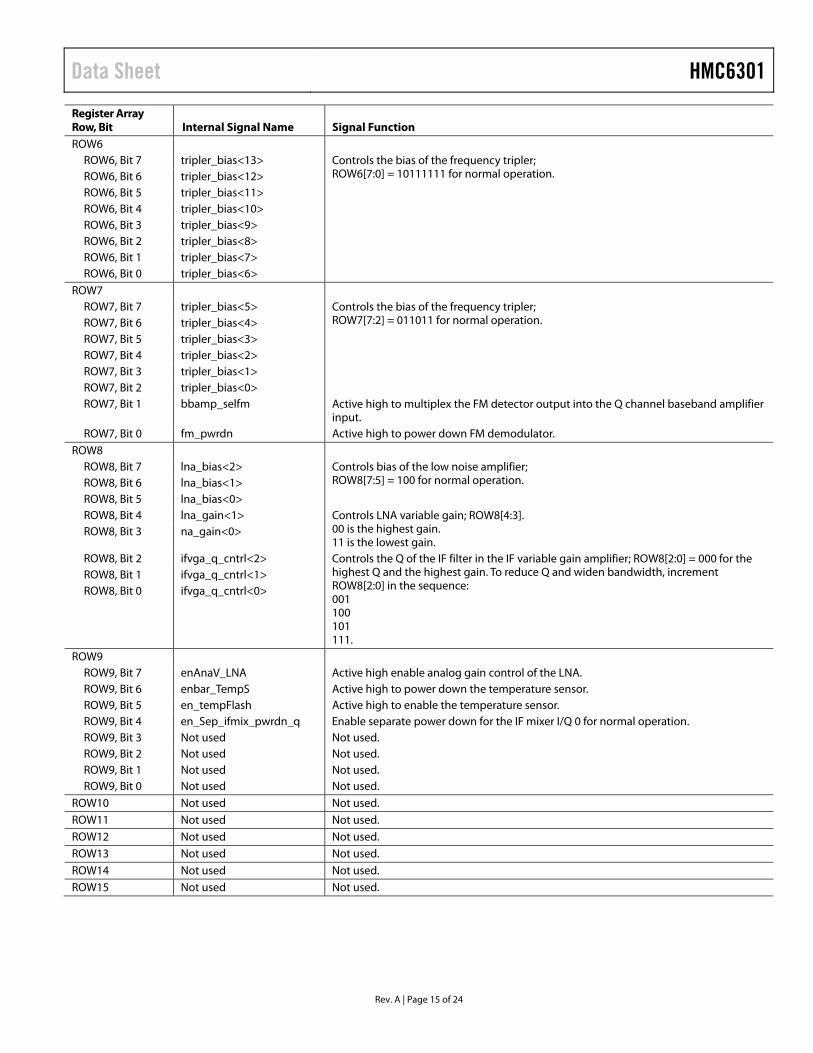
Rev. A | Page 15 of 24
Register Array Row, Bit Internal Signal Name Signal Function ROW6
ROW6, Bit 7 tripler_bias<13> Controls the bias of the frequency tripler; ROW6[7:0] = 10111111 for normal operation. ROW6, Bit 6 tripler_bias<12>
ROW6, Bit 5 tripler_bias<11> ROW6, Bit 4 tripler_bias<10> ROW6, Bit 3 tripler_bias<9> ROW6, Bit 2 tripler_bias<8> ROW6, Bit 1 tripler_bias<7> ROW6, Bit 0 tripler_bias<6>
ROW7 ROW7, Bit 7 tripler_bias<5> Controls the bias of the frequency tripler;
ROW7[7:2] = 011011 for normal operation. ROW7, Bit 6 tripler_bias<4> ROW7, Bit 5 tripler_bias<3> ROW7, Bit 4 tripler_bias<2> ROW7, Bit 3 tripler_bias<1> ROW7, Bit 2 tripler_bias<0> ROW7, Bit 1 bbamp_selfm Active high to multiplex the FM detector output into the Q channel baseband amplifier
input. ROW7, Bit 0 fm_pwrdn Active high to power down FM demodulator.
ROW8 ROW8, Bit 7 lna_bias<2> Controls bias of the low noise amplifier;
ROW8[7:5] = 100 for normal operation. ROW8, Bit 6 lna_bias<1> ROW8, Bit 5 lna_bias<0> ROW8, Bit 4 lna_gain<1> Controls LNA variable gain; ROW8[4:3].
00 is the highest gain. 11 is the lowest gain.
ROW8, Bit 3 na_gain<0>
ROW8, Bit 2 ifvga_q_cntrl<2> Controls the Q of the IF filter in the IF variable gain amplifier; ROW8[2:0] = 000 for the highest Q and the highest gain. To reduce Q and widen bandwidth, increment ROW8[2:0] in the sequence: 001 100 101 111.
ROW8, Bit 1 ifvga_q_cntrl<1> ROW8, Bit 0 ifvga_q_cntrl<0>
ROW9 ROW9, Bit 7 enAnaV_LNA Active high enable analog gain control of the LNA. ROW9, Bit 6 enbar_TempS Active high to power down the temperature sensor. ROW9, Bit 5 en_tempFlash Active high to enable the temperature sensor. ROW9, Bit 4 en_Sep_ifmix_pwrdn_q Enable separate power down for the IF mixer I/Q 0 for normal operation. ROW9, Bit 3 Not used Not used. ROW9, Bit 2 Not used Not used. ROW9, Bit 1 Not used Not used. ROW9, Bit 0 Not used Not used.
ROW10 Not used Not used. ROW11 Not used Not used. ROW12 Not used Not used. ROW13 Not used Not used. ROW14 Not used Not used. ROW15 Not used Not used.

HMC6301 Data Sheet
Rev. A | Page 16 of 24
Register Array Row, Bit Internal Signal Name Signal Function ROW16
ROW16, Bit 7 byp_synth_LDO Factory diagnostics, 0 for normal operation. ROW16, Bit 6 en_cpShort Factory diagnostics, 0 for normal operation. ROW16, Bit 5 en_cpCMFB Enables CMFB circuit for charge pump, set to 1 when synthesizer is in use. ROW16, Bit 4 en_cp_dump Enables auxiliary circuit for charge pump, set to 1 when synthesizer is in use. ROW16, Bit 3 en_cpTRIST Factory diagnostics, 0 for normal operation. ROW16, Bit 2 en_cp Enables charge pump, set to 1 when synthesizer is in use. ROW16, Bit 1 en_synth_LDO Enables LDO for synthesizer, set to 1 when synthesizer is in use. ROW16, Bit 0 enbar_synthBG Factory diagnostics, 0 for normal operation.
ROW17 ROW17, Bit 7 en_lockd_clk Enables lock detector for synthesizer, set to 1 when synthesizer is in use. ROW17, Bit 6 en_test_divOut Factory diagnostics, 0 for normal operation. ROW17, Bit 5 en_vtune_flash Enables flash ADCs for VCO vtune port, set to 1 when synthesizer is in use. ROW17, Bit 4 en_reBuf_DC Enables dc coupling for reference clock buffer. ROW17, Bit 3 en_refBuf Enables reference clock buffer, set to 1 when synthesizer is in use. ROW17, Bit 2 en_stick_div Factory diagnostics, 0 for normal operation. ROW17, Bit 1 en_FBDiv_cml2cmos Enables auxiliary circuit for the feedback divider chain, set to 1 when synthesizer is in use. ROW17, Bit 0 en_FBDiv Enables feedback divider chain, set to 1 when synthesizer is in use.
ROW18 ROW18, Bit 7 Not used. Not used. ROW18, Bit 6 en_nb250m Active high to enable 250 MHz channel step size. ROW18, Bit 5 byp_vco_LDO Factory diagnostics, 0 for normal operation. ROW18, Bit 4 en_extLO Enables external LO, set to 0 when synthesizer is in use. ROW18, Bit 3 en_vcoPk Factory diagnostics, 0 for normal operation. ROW18, Bit 2 en_vco Enables internal VCO, set to 1 when synthesizer is in use. ROW18, Bit 1 en_vco_reg Enables internal regulator for VCO, set to 1 when synthesizer is in use. ROW18, Bit 0 enbar_vcoGB Factory diagnostics, 0 for normal operation.
ROW19 ROW19, Bit 7 Not used Not used. ROW19, Bit 6 Not used Not used. ROW19, Bit 5 Not used Not used. ROW19, Bit 4 Not used Not used. ROW19, Bit 3 Not used Not used. ROW19, Bit 2 Not used Not used. ROW19, Bit 1 refsel_synthBG Factory diagnostics, 1 for normal operation. ROW19, Bit 0 muxRef Factory diagnostics, 0 for normal operation.
ROW20 ROW20, Bit 7 Not used Not used. ROW20, Bit 6 Fbdiv_code<6> Feedback divider ratio for the integer-N internal synthesizer based on Table 7, Table 8,
and Table 9. ROW20, Bit 5 Fbdiv_code<5> ROW20, Bit 4 Fbdiv_code<4> ROW20, Bit 3 Fbdiv_code<3> ROW20, Bit 2 Fbdiv_code<2> ROW20, Bit 1 Fbdiv_code<1> ROW20, Bit 0 Fbdiv_code<0>

Data Sheet HMC6301
Rev. A | Page 17 of 24
Register Array Row, Bit Internal Signal Name Signal Function ROW21
ROW21, Bit 7 Not used Not used. ROW21, Bit 6 Not used Not used. ROW21, Bit 5 Not used Not used. ROW21, Bit 4 refsel_vcoBG Factory diagnostics, 1 for normal operation. ROW21, Bit 3 vco_biasTrim<3> Sets VCO tank bias current ROW21[3:0] = 0010 for normal operation. ROW21, Bit 2 vco_biasTrim<2> ROW21, Bit 1 vco_biasTrim<1> ROW21, Bit 0 vco_biasTrim<0>
ROW22 ROW22, Bit 7 Not used Not used. ROW22, Bit 6 Not used Not used. ROW22, Bit 5 Not used Not used. ROW22, Bit 4 vco_bandSel<4> Set for desired frequency. Table 7, Table 8, and Table 9. contain approximate band
setting depending on reference clock frequency. ROW22[4:0] = valid range 00000-10011.
ROW22, Bit 3 vco_bandSel<3> ROW22, Bit 2 vco_bandSel<2> ROW22, Bit 1 vco_bandSel<1> ROW22, Bit 0 vco_bandSel<0>
ROW23 ROW23, Bit 7 ICP_BiasTrim<2> Sets charge pump current. ROW23[7:5] = 011 for normal operation. ROW23, Bit 6 ICP_BiasTrim<1> ROW23, Bit 5 ICP_BiasTrim<0> ROW23, Bit 4 vco_offset<0> Sets internal VCO output swing. ROW23[4:0] = 00010 for normal operation. ROW23, Bit 3 vco_offset<1> ROW23, Bit 2 vco_offset<2> ROW23, Bit 1 vco_offset<3> ROW23, Bit 0 vco_offset<4>
ROW24 (Read Only) ROW24, Bit 7 Not used Not used. ROW24, Bit 6 Not used Not used. ROW24, Bit 5 Not used Not used. ROW24, Bit 4 Not used Not used. ROW24, Bit 3 lockdet Monitor for lock detect, 1 indicates valid lock. ROW24, Bit 2 dn Monitor VCO amplitude. ROW24, Bit 1 up Monitor VCO amplitude. ROW24, Bit 0 center Monitor VCO amplitude.
ROW25 (Read Only) ROW25, Bit 7 vtune_flashp<7> VCO amplitude monitor (positive). ROW25, Bit 6 vtune_flashp<6> ROW25, Bit 5 vtune_flashp<5> ROW25, Bit 4 vtune_flashp<4> ROW25, Bit 3 vtune_flashp<3> ROW25, Bit 2 vtune_flashp<2> ROW25, Bit 1 vtune_flashp<1> ROW25, Bit 0 vtune_flashp<0>

HMC6301 Data Sheet
Rev. A | Page 18 of 24
Register Array Row, Bit Internal Signal Name Signal Function ROW26 (Read Only)
ROW26, Bit 7 vtune_flashn<7> VCO amplitude monitor (negative). ROW26, Bit 6 vtune_flashn<6> ROW26, Bit 5 vtune_flashn<5> ROW26, Bit 4 vtune_flashn<4> ROW26, Bit 3 vtune_flashn<3> ROW26, Bit 2 vtune_flashn<2> ROW26, Bit 1 vtune_flashn<1> ROW26, Bit 0 vtune_flashn<0>
ROW27 (Read Only) ROW27, Bit 7 Not used Not used. ROW27, Bit 6 Not used Not used. ROW27, Bit 5 Not used Not used. ROW27, Bit 4 tempS<4> Thermometer encoded temperature reading.
ROW27[4:0] = the following: 00000 is the lowest temperature. 11111 is the highest temperature.
ROW27, Bit 3 tempS<3> ROW27, Bit 2 tempS<2> ROW27, Bit 1 tempS<1> ROW27, Bit 0 tempS<0>
ROW28 Not used Not used. ROW29 Not used Not used. ROW30 Not used Not used. ROW31 Not used Not used.

Data Sheet HMC6301
Rev. A | Page 19 of 24
Synthesizer Settings
Table 7. Synthesizer Settings, IEEE Channels Using 154.2857 MHz Reference
Frequency (GHz) IEEE Channel Divider Setting, Fbdiv_Code<5:0>, ROW20, Bits[5:0]
Typical Band Setting, vco_bandSel<4:0>, ROW22, Bits[4:0]
57.24 001010 00001 57.78 001011 00010 58.32 Channel 1 001100 00010 58.86 001101 00010 59.40 001110 00011 59.94 001111 00011 60.48 Channel 2 010000 00100 61.02 010001 00100 61.56 010010 00101 62.10 010011 00101 62.64 Channel 3 010100 00101 63.18 010101 00110 63.72 010110 00110 64.26 010111 00110 64.8 Channel 4 011000 00111 65.34 011001 00111 65.88 011010 01000
Table 8. 500 MHz Channels Using 142.8571 MHz Reference Frequency (GHz) Divider Setting Typical Band Setting 56.5 010001 00001 57 010010 00001 57.5 010011 00010 58 010100 00010 58.5 010101 00010 59 010110 00011 59.5 010111 00011 60 011000 00100 60.5 011001 00100 61 011010 00101 61.5 011011 00101 62 011100 00101 62.5 011101 00110 63 011110 00110 63.5 011111 00110 64 100000 00111

HMC6301 Data Sheet
Rev. A | Page 20 of 24
Table 9. 250 MHz Channels Using 71.42857 MHz Reference Frequency (GHz) Divider Setting Typical Band Setting 56.5 0100010 00001 56.75 0100011 00001 57 0100100 00010 57.25 0100101 00010 57.5 0100110 00011 57.75 0100111 00011 58 0101000 00100 58.25 0101001 00100 58.5 0101010 00101 58.75 0101011 00101 59 0101100 00110 59.25 0101101 00110 59.5 0101110 00111 59.75 0101111 00111 60 0110000 01000 60.25 0110001 01000 60.5 0110010 01001 60.75 0110011 01001 61 0110100 01010 61.25 0110101 01010 61.5 0110110 01011 61.75 0110111 01011 62 0111000 01100 62.25 0111001 01100 62.5 0111010 01101 62.75 0111011 01101 63 0111100 01110 63.25 0111101 01110 63.5 0111110 01111 63.75 0111111 01111 64 1000000 01111

Data Sheet HMC6301
Rev. A | Page 21 of 24
APPLICATIONS INFORMATION For more information about the HMC6301 evaluation kit, see the EK1HMC6350 User Guide. The EK1HMC6350 contains all that is required to set up a simplex 60 GHz millimeterwave link using standard RF cable interfaces for baseband input and output. The kit comes with two motherboard printed circuit
boards (PCBs) that provide on-board crystals, USB interface, supply regulators, and SMA cables for connectorized I/Q interfaces. Software is supplied to allow the user to read from and write to all chip level registers using graphical user interface (GUI) or to upload previously saved register settings.
600-01362-00-1
RX IN
EXTLO_P EXTLO_N
RX MODULE
R3
C1
C2C7C14
R1
C13C11C9
C10R2
C4 C5C1
2C3C8
C6
J1
U1
J2J3
C15C16
1442
4-01
9
Figure 19. HMC6301 (600-01362-00-1) Evaluation PCB Daughter Board

HMC6301 Data Sheet
Rev. A | Page 22 of 24
RFIN
ANACTL_LNA
EXTFIL_PEXTFIL_N
EXTLO_NEXTLO_P
DATA
CLKENABLE
RESET
REF_CLKPREF_CLKN
VDDD
SCANOUT
VCC_BUFACTL_IFVGA
VCC_MIXVCC_IF
VCO_RCAP
VCC_TRIPVCC_LNA
VREG_OUT
VOUT_QMVOUT_QP
VOUT_IMVOUT_IP
GND
VCC_DIV
VDD_SYN
VSS_DIV
GNDGNDGNDGNDGNDGNDGNDGNDGND
GND
VSS_DIVVSS_DIVVSS_DIV
VDD_SYN
VCC_DIV
VCC_DIV
VCC_DIVVCC_DIV
VCC_DIVVSS_CPVSS_CP
VSS_LPFVSS_LPFVSS_LPFVSS_LPF
VSS_REFVSS_REF
VSS_VCOVSS_VCO
VCC_VCOVCC_VCO
VSS_VCOVSS_VCOVSS_VCOVSS_VCOVSS_VCO
VCC_DIV
R11kΩDEPOP
R21kΩDEPOP
92_MMPX-S50-0-1/111_NM-1
J5
EXTFL_P
RX_IN
GNDGNDGNDGNDGNDGNDGNDGNDGNDGNDGND
U1HMC6301
A12
H12H11H10
H9H6
G10G9
G8G7
F11F10
D12D11D10
D9
E11E10
A7A6
A10
A4A3
B3
G6
H2
B4D1B6B7F1G2G4H1H5
C1
C12C11C10C9
G12F9
B12B11B10
A11
G5
A9
G11
H3
G3
H4
A5
A2
B5
F12E12
A8
B1
A1
B2
H8H7
B9B8
G1
E1VOUT_QPVOUT_QM
VOUT_IPVOUT_IM
C21nF
C31nF
C41nF
C51nF
C61nF
C71nF
C81nF
100pF
C9
C10100nF
C11100nF
RX_VCC_LNA
ACTL_IFVGA
RX_VCC_DIV
RX_VCC_IF
RX_VCC_MIX
RX_VCC_BUFDATA
CLK
ENABLE
RESET
RX_REFCLKMRX_REFCLKP
RX_SCANOUT
ACTL_LNA
C121nF
C131nF RX_VDDD
EXTLO_P
EXTLO_N
RX_VDD_SYN
VSS_GND
VSS_GND
R3
0
RX_VCC_TRIP
RX_VCC_VCO
J2SMA
SMAJ3
VSS_GND
EXTFL_N
1nFC14
C11µF
DEPOP
13579
2468
101214161820
GR
OU
ND
BU
S34323028262422
59575553514947454341393735333129272523211917151311
QTH-030-01-F-D-AJ4
60585654525048464442403836
ACTL_IFVGA
GND
GND
GNDGNDGNDGNDGND
GNDGNDGNDGNDGNDGNDGNDGNDGNDGNDGND
GND
GND
GND
GND
ACTL_LNA
VOUT_QM
VOUT_QP
VOUT_IM
VOUT_IP
NC
GND
GNDGND
GNDGND
GND
GND
GND
GNDGND
GND
RX_VCC_BUF
RX_VDDD
RX_VCC_IF
RX_VCC_LNA
RX_VDD_SYN
RX_SCANOUTDATA
CLKENABLE
RESET
RX_VCC_DIV
RX_VCC_VCO
RX_VCC_TRIP
RX_VCC_MIX
RX_REFCLKP
RX_REFCLKM
1442
4-02
0
Figure 20. HMC6301 Evaluation PCB Schematic

Data Sheet HMC6301
Rev. A | Page 23 of 24
USB-LED
PWR-SUPPLY-LED
SEL1MUX
USB
5V SUPPLY
EXT CLOCK
VOUT IPVOUT IM
BB QP BB IM BB IP
VOUT QPVOUT QM
FMP Q FMM QFMM IFMP IBB QM
600-01205-00-2
MUXSEL0
121 2
RX MODULE
TX MODULE
DECT OUT
REF OUT
TX IFVGA
TX RFVGA
RX LNA CTL
RX IFVGA
60 GHz EVALUATION BOARD
1 26059
+
++
+
++
++
1260 59
R15
5
C82
R15
9
R88J28
C2
C9
J20
FB1
FB2 FB4
FB6
C1
C10 C11
C12
C13
C14
C21 C85
C88
C24C25
C26
C28
C3
C86
C4
C42
C43
C44
C45
C46
C47
C48
C49
C5
C50C51
C52
C6
C63
C64
C65
C66
C67
C68
C69
C7
C70
C89
C8
C58
C93
C90
C56
U3
U15
U16
D1
D4
D7
D8
J8
R119
R15
7
R161
R13
R15
R17
R19
R21R22
R23
R24
R56
R57R58
R69
R62
R63
R64R65
R66
R68
R67
R70
R71
R72
R73
R131
R82
R85
R86
R87R89
R90
R91R92
R93
R94
R95
R96
R97R98
R99
R167
R178
R12
3
R12
8R
129R
14R
16R
18R
20
R32
R59
R77
R103
R61
R79
J10J11 J12
J13J14J15 J16 J17 J18 J19
J21 J9
U19
J26
J27
J1
Y1
R180
R166
R169R168
R176
R183
R177
R172
R184
R181
R175R174
R170R171
C84
C87
Y4
Y3
U17
U18
U11
R15
3R
152
C79
R15
8
J30C80
C81
C83
C91
C92
C95
C94
R130
R15
4
R15
6
R160
R162
R163
R60
R165
R173
R182
R179
R164
U22
J31
J32
J33
J34
J29
C10
2
C101
C110
C96
C105
C99
C108
C10
3
C97
C10
6
C10
0
C10
9
U27
U26
U23
U24
R18
6
R19
5
R18
8R
189 R
187
R190
R19
1
R19
2R
193
U25
C104
C98
C107R194
R185
1442
4-02
1
Figure 21. HMC6301 Evaluation PCB Motherboard
HMC6301 Data Sheet
Rev. A | Page 24 of 24
OUTLINE DIMENSIONS
0.8150.7550.695
6.0506.0005.950
BOTTOM VIEW(BALL SIDE UP)
TOP VIEW(BALL SIDE DOWN)
SIDE VIEW
0.2200.1900.160
0.5950.5650.535
0.3100.2700.230
4.0504.0003.950
3.50REF
5.50 REF
5.75 REF
COPLANARITY0.10
SEATINGPLANE
01
-25
-201
6-A
0.50BSC
0.25BSC
0.25 BSC
PK
G-0
05
03
0
0.50 BSC
0.40 BSC
BALL A1IDENTIFIER 0.65
0.15
0.25 0.6350.485
GROUNDAREA
A
B
C
D
E
F
G
H
123456789101112
Figure 22. 75-Ball Wafer Level Ball Grid Array [WLBGA]
(BF-75-1) Dimensions shown in millimeters
ORDERING GUIDE
Model Temperature Range Chip Bump Composition
MSL Rating1 Package Description
Package Option Package Marking2
HMC6301BG46 −40°C to +85°C 96.5 Tin (Sn), 3.0 Silver (Ag), 0.5 Copper (Cu)
MSL1 75-Ball WLBGA BF-75-1 BBFZ
#YYWW
XXX XXXXX-XX
EV1HMC6301BG46 Evaluation Board, PCB Only EK1HMC6350 Evaluation Kit Assembly 1 Maximum peak reflow temperature of 260°C. The peak reflow temperature must not exceed the maximum temperature for which the package is qualified according
to the moisture sensitivity level (MSL1). 2 BBFZ indicates a Pb-free part, #YYWW indicates the year and week number, and the assembly lot number is indicated by XXX XXXXXX-XX.
©2016 Analog Devices, Inc. All rights reserved. Trademarks and registered trademarks are the property of their respective owners. D14424-0-9/16(A)
Recommended