Microprocessor-Based Systems
Dr. Randa Elanwar
Lecture 5

Lecture Content
• RISC and CISC architectures
• External memory
– memory segmentation
– memory address decoding
– Instruction codes
• Application examples
2Microprocessor-Based Systems Dr. Randa Elanwar

Microprocessor bus architecture and instruction sets
3Microprocessor-Based Systems Dr. Randa Elanwar
As we have seen so far: The execution unit of the microprocessor (EU) has 8 general purpose registers working as temporary storage (i.e., internal memory): AH, AL, BH, BL, CH, CL, DH and DL. They can be used individually (8 bit mode) or in couples (16 bit mode)
AL register is called the accumulator. It has some extra features not found in others.
The data stored in these registers (internal memory) is accessed much more quickly than being accessed if it is stored in the external memory

RISC vs. CISC• An important aspect of computer architecture is the design of the
instruction set for the processor. • The instruction set chosen for a particular computer determine
the way that machine language programs are constructed. • Early computers had small and simple instruction sets, forced
mainly by the need to minimize the hardware used to implement them.
• A computer with a large number of instructions is classified as a Complex Instruction Set Computer, abbreviated CISC.
• In the early 1980s, a number of computer designers recommended that computers use fewer instructions with simple constructs so they can be executed much faster within the CPU without having to use memory as often. This type of computer is classified as a Reduced Instruction Set Computer or RISC.
4Microprocessor-Based Systems Dr. Randa Elanwar

RISC vs. CISC• The essential goal of a CISC architecture is to attempt to provide a
single machine instruction for each statement that is written in a high-level language, in other words, try to be in almost no need of a compiler.
• The translation from high-level programming language to machine language programs is done by means of a compiler program.
• The major characteristics of CISC architecture are:• 1. A large number of instructions-typically from 100 to 250
instructions• 2. Some instructions that perform specialized tasks and are used
infrequently• 3. A large variety of addressing modes-typically from 5 to 20
different modes• 4. Variable-length instruction formats• 5. Instructions that manipulate operands in memory
5Microprocessor-Based Systems Dr. Randa Elanwar

RISC vs. CISC
• The concept of RISC architecture involves an attempt to reduce execution time by simplifying the instruction set of the computer.
• The major characteristics of a RISC processor are:
• 1. Relatively few instructions
• 2. Relatively few addressing modes
• 3. Memory access limited to load and store instructions
• 4. All operations done within the registers of the CPU
• 5. Fixed-length, easily decoded instruction format
• 6. Single-cycle instruction execution
• 7. Hardwired rather than microprogrammed control6Microprocessor-Based Systems Dr. Randa Elanwar

RISC vs. CISC
• A characteristic of RISC processors is their ability to execute one instruction per clock cycle. This is done by overlapping the fetch, decode and execute phases of two or three instructions by using a procedure referred to as pipelining.
• Other characteristics attributed to RISC architecture are:
• 1. A relatively large number of registers in the processor unit
• 2. Efficient instruction pipeline
• 3. Compiler support for efficient translation of high-level language programs into machine language programs.
7Microprocessor-Based Systems Dr. Randa Elanwar

External memory
• The external memory (outside the microprocessor) is composed of a large number of registers.
• If the memory has 4000 8-bits storage locations for example, it is referred to as 4K byte memory.
• The number of memory locations the can be addressed by the microprocessor is determined by the number of address lines it has.
• If the microprocessor 16 address lines bus (A0 to A15) it can address up to 216 locations (26*210) = 64K byte memory.
8Microprocessor-Based Systems Dr. Randa Elanwar
Memory address (Bin) (Hex) Stored data (Bin) (Hex)0000 0000 0000 0000 0000 0010 1011 2B
…. …. …. …. …. …. …. ….…. …. …. …. …. …. …. ….
1111 1111 1111 1111 FFFF 0000 0010 02

Memory Address decoding
• Decoders have n-inputs and 2n outputs, each input combination results in a single output line having a 1, all other lines have a 0 on the output.
• The memory decoder is connected to the CPU by the address bus.
• Each memory cell is connected to an input and output data bus, a read/write control, and the decoder which enables the memory cell when the appropriate address appears.
• The decoder ensures that only a single memory cell is activated at a time for either input or output.
9Microprocessor-Based Systems Dr. Randa Elanwar
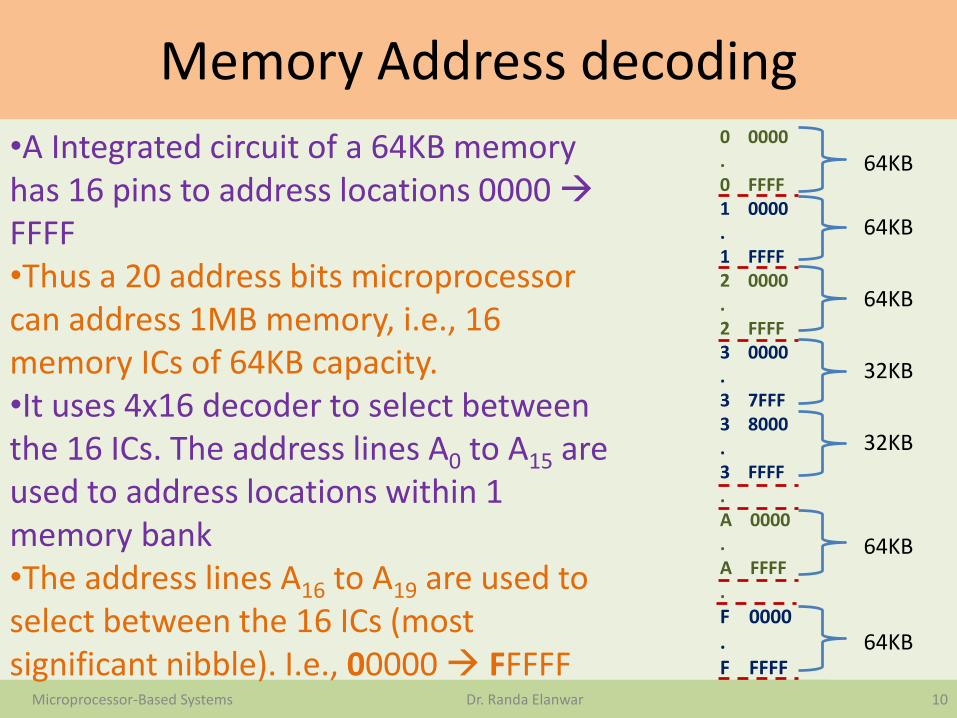
Memory Address decoding
10Microprocessor-Based Systems Dr. Randa Elanwar
•A Integrated circuit of a 64KB memory has 16 pins to address locations 0000 FFFF•Thus a 20 address bits microprocessor can address 1MB memory, i.e., 16 memory ICs of 64KB capacity.•It uses 4x16 decoder to select between the 16 ICs. The address lines A0 to A15 are used to address locations within 1 memory bank •The address lines A16 to A19 are used to select between the 16 ICs (most significant nibble). I.e., 00000 FFFFF
0 0000.0 FFFF1 0000.1 FFFF2 0000.2 FFFF3 0000.3 7FFF3 8000.3 FFFF.A 0000.A FFFF.
F 0000.F FFFF
64KB
64KB
64KB
64KB
64KB
32KB
32KB

Memory Address decoding
• If two Integrated circuit of a 32KB memory are used instead of a single Integrated circuit of a 64KB memory, the A15 address bit is used to select between them.
11Microprocessor-Based Systems Dr. Randa Elanwar
8088
0 00000 FFFF
64KBA0
.A15
MEMR
MEMW 1 00001 FFFF
64KB
2 00002 FFFF
64KB
3 00003 7FFF
32KB
3 80003 FFFF
32KB
4x16 decoder
A16
.A19
A15 A15
012.F
CS CS
CS CS

8088 address bus and Memory segmentation
• 8086 microprocessor has 16 bit internal bus and 16 bit external bus.
• 8088 microprocessor has 16 bit internal bus and 8 bit external bus.
12Microprocessor-Based Systems Dr. Randa Elanwar
Control LogicCreates the addresses
8088 microprocessor
Data bus
Memoryholds data and
instructions
Address lines
MEMR
MEMW

8088 address bus and Memory segmentation
• All memory locations are connected on the common bus such that only one location can output its content on the bus and all ALSU structure is isolated (i.e., only one location at a time).
• The memory locations addresses are usually included in arithmetic operations (specially INC operation).
• The 20 address lines give out address of 5 hex digits (00000 FFFFF).
• If address lines has 00000 and MEMR is low, then the first memory location is selected to output its content on the bus.
• Programs (instructions sequence) stored in memory are coded in binary/hex format to be transmitted on the data bus to the microprocessor EU so that it can be decoded and executed
13Microprocessor-Based Systems Dr. Randa Elanwar

Instruction codes
• Instruction Operation
• INC r16 increments the content of a 16 bit register,
r16 represent the register name
• Example:
• INC AX Code: 0100 0000 Hex: 40
• INC SI Code: 0100 0110 Hex: 46
14Microprocessor-Based Systems Dr. Randa Elanwar
Register 16 bit mode
8 bit mode
000 AX AL
001 CX CL
010 DX DL
011 BX BL
100 SP AH
101 BP CH
110 SI DH
111 DI BH
0 1 0 0 0
INC instruction code
Register name code

Instruction codes
• Instruction Operation
• INC r8 increments the content of a 8 bit register,
r8 represent the register name
• Example:
• INC AL Code: 1111 1110 1100 0000 Hex: FEC0
• INC AH Code: 1111 1110 1100 0110 Hex: FEC4
• Instruction codes can consist of one, two, three or four bytes.
15Microprocessor-Based Systems Dr. Randa Elanwar
1 1 0 0 0
INC instruction code
Register name code
1 1 1 1 1 1 1 0

Instruction codes
• MOV AL, [2FB70]
– This instruction reads the content of the memory location address 2FB70 and stores them in AL
– The content of the memory location address is 1 byte (2 hex digits).
– Address lines will hold: 0010 1111 1011 0111 0000
• MOV [2FB70], AL
– This instruction writes the content of AL into the memory location address 2FB70
• If we want to write a part of a program into the memory:
16Microprocessor-Based Systems Dr. Randa Elanwar
Memory Address Content
2B37E FE
2B37F C4
2B380 46
Data or instruction
INC AH
INC SI
Instruction codes
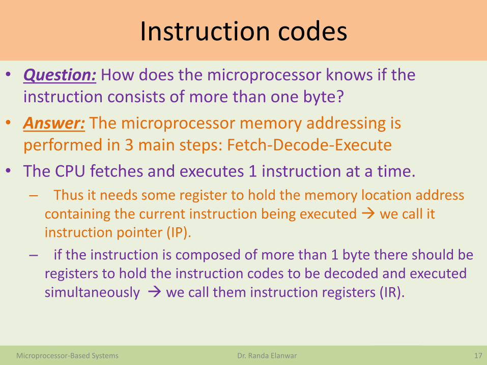
• Question: How does the microprocessor knows if the instruction consists of more than one byte?
• Answer: The microprocessor memory addressing is performed in 3 main steps: Fetch-Decode-Execute
• The CPU fetches and executes 1 instruction at a time.
– Thus it needs some register to hold the memory location address containing the current instruction being executed we call it instruction pointer (IP).
– if the instruction is composed of more than 1 byte there should be registers to hold the instruction codes to be decoded and executed simultaneously we call them instruction registers (IR).
17Microprocessor-Based Systems Dr. Randa Elanwar

Instruction codes
18Microprocessor-Based Systems Dr. Randa Elanwar
Control LogicCreates the addresses
8088 microprocessor
Data bus
Memoryholds data
and instructionsAddress
lines
MEMR
MEMW
IR1 IR0…
IP
IR4
1. The IP register content is output on the address lines
2. The control logic activates the read signal (MEMR is low)
3. The control logic clocks IR0 and stores the instruction first byte
4. The control logic reads the output of IR0 and determines whether or not the instruction is complete
5. If the instruction is not yet complete, IP is incremented
6. When the instruction is complete, the CPU checks the instruction table, decodes the instruction and executes it by operating ALSU
Memory segmentation, address decoding and direct access
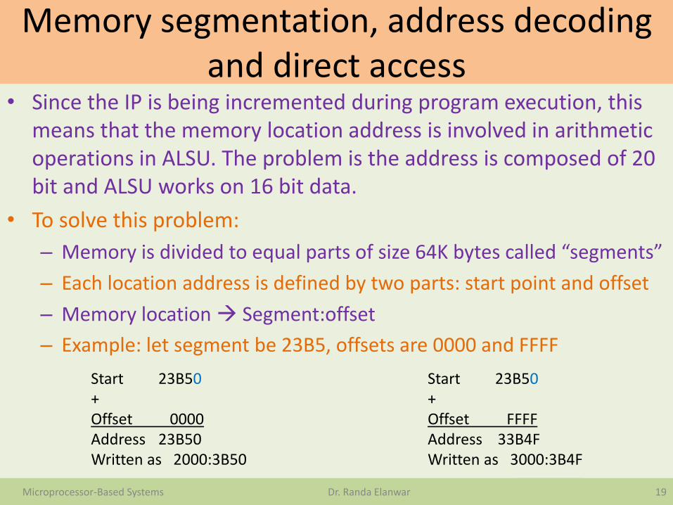
• Since the IP is being incremented during program execution, this means that the memory location address is involved in arithmetic operations in ALSU. The problem is the address is composed of 20 bit and ALSU works on 16 bit data.
• To solve this problem:
– Memory is divided to equal parts of size 64K bytes called “segments”
– Each location address is defined by two parts: start point and offset
– Memory location Segment:offset
– Example: let segment be 23B5, offsets are 0000 and FFFF
19Microprocessor-Based Systems Dr. Randa Elanwar
Start 23B50 Start 23B50+ +Offset 0000 Offset FFFFAddress 23B50 Address 33B4FWritten as 2000:3B50 Written as 3000:3B4F

Memory segmentation, address decoding and direct access
• Now it is easy to perform arithmetic operations on the address.
• Example:
• We have four segment registers in the BIU are used to hold the upper 4 bytes of the address:
– CS: Code segment register
– SS: Stack segment register
– ES: Extra segment register
– DS: Data segment register
20Microprocessor-Based Systems Dr. Randa Elanwar
Memory Address Content Seg:offset
2B37E FE 2000:B37E
2B37F C4 2000:B37F
2B380 46 2000:B380

Memory segmentation, address decoding and direct access
• The BIU always insert zeros for the lowest nibble of the 20 bit starting address for a segment.
21Microprocessor-Based Systems Dr. Randa Elanwar
RegisterName
Code Segment (CS)
Stack Segment (SS)
Extra Segment (ES)
Data Segment (DS)
Function
Holds the upper 16 bits of the startingaddress for the segment from which the BIU is currently fetching instruction codes
Holds the upper 16 bits of the starting address for the program stack (Stack stores program addresses and data while subprogram executes)
Holds the upper 16 bits of the starting address for the memory segment used for data storage
Holds the upper 16 bits of the starting address for the memory segment used for data storage

Memory segmentation, address decoding and direct access
22Microprocessor-Based Systems Dr. Randa Elanwar
CS
DS
ES
SS
IP
T3
BP
SP
Segment registers (16 bits)
Offset registers (16 bits)
MUX MUX
HA HA HA HA FA FA HA…
20 bit address latch
44444444
444 44c c c c c
A0
.
.A19
8088 microprocessor F0000-FFFFF
E0000-EFFFFD0000-DFFFFC0000-CFFFFB0000-BFFFFA0000-AFFFF90000-9FFFF80000-8FFFF70000-7FFFF60000-6FFFF50000-5FFFF40000-4FFFF30000-3FFFF20000-2FFFF10000-1FFFF00000-0FFFF
20 address lines 220 bytes 24+6+10
16 segments of external memory, each is 64K bytes

Memory segmentation, address decoding and direct access
• The micro-operations of memory access:
• Example: MOV AH, [BX]
– BX contains the offset only since DS has the segment start point
1. BX content is moved to T3
2. MUX is activated to add T3 and DS
3. The physical address comes out
4. MEMR signal goes low
5. The CLKAH goes low
23Microprocessor-Based Systems Dr. Randa Elanwar

Memory segmentation, address decoding and direct access
• The micro-operations of memory access:
• Example: MOV AH, [BX+SI-17]
1. BX content is added to SI and result is moved to T1
2. 17 is complemented and added to T1 and result is moved to T3 (now we have the offset)
3. MUX is activated to add T3 and DS
4. The physical address comes out
5. MEMR signal goes low
6. The CLKAH goes low
24Microprocessor-Based Systems Dr. Randa Elanwar

Application Examples
• Write a program to add a data byte located at offset 0500H in 2000H segment to another data byte available at 0600H in the same segment and store the result at 0700H in the same segment
25Microprocessor-Based Systems Dr. Randa Elanwar

Application Examples
• As the immediate data cannot be loaded into a segment register, the data is transferred to one of the general purpose resistors, say AX. and then the register general purpose registers, say AX, and then the register content is moved to the segment register DS. Thus the data segment register DS contains 2000H.
• The instruction MOV AX,[500H] signifies that the contents of the particular location, whose offset is specified in the brackets with the segment pointed to by DS as segment register, is to be moved to AX.
• The MOV [0700], AX instruction moves the contents of the register AX to an offset 0700H in DS (DS = 2000H).
26Microprocessor-Based Systems Dr. Randa Elanwar

Application Examples
• Write a program to move the contents of the memory location 0500H to register BX and also to CX. Add immediate byte 05H to the data residing in memory location, whose address is computed using DS=2000H and offset=0600H. Store the result of the addition in 0700H. Assume that the data is located in the segment specified by the data segment register which contain 2000H.
27Microprocessor-Based Systems Dr. Randa Elanwar

Application Examples
• The immediate data byte 05H is added to content of 0600H using the ADD instruction. The result will be in the destination operand 0600H. This is next stored at the location 0700H.
• In case of the 8086/8088 instruction set, there is no instruction for the direct transfer of data from the memory source operand to the memory destination operand except, the string instructions.
• Hence the result of addition which is present at 0600H, should be moved to any one of the general purpose registers, except BX and CX, otherwise the contents of CX and BX will be changed (We have selected DX).
• Thus the transfer of result from 0600H to 0700H is accomplished in two stages using successive MOV instructions i.e., first, the content of 0600H is DX and then the content of DX is moved to 0700H.
28Microprocessor-Based Systems Dr. Randa Elanwar
Application Examples
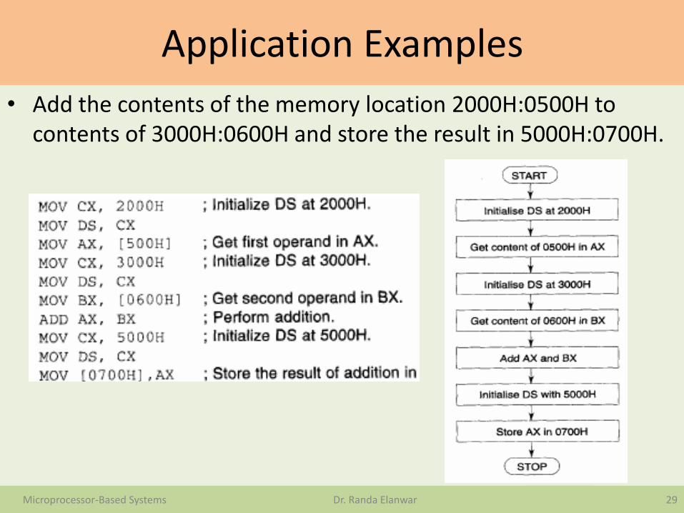
• Add the contents of the memory location 2000H:0500H to contents of 3000H:0600H and store the result in 5000H:0700H.
29Microprocessor-Based Systems Dr. Randa Elanwar

Application Examples
• Write a program for addition of two numbers
30Microprocessor-Based Systems Dr. Randa Elanwar
Beginning of data initialization
End of data initialization
Application Examples
• Write a program for addition of two numbers
31Microprocessor-Based Systems Dr. Randa Elanwar
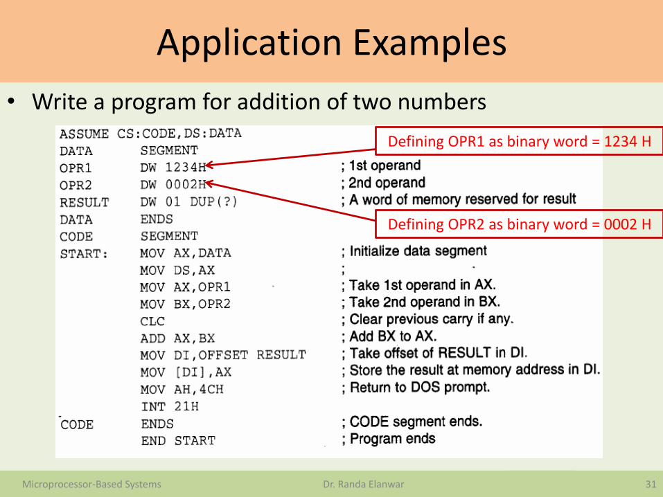
Defining OPR1 as binary word = 1234 H
Defining OPR2 as binary word = 0002 H
Application Examples
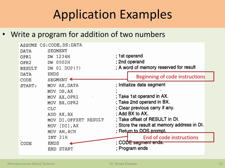
• Write a program for addition of two numbers
32Microprocessor-Based Systems Dr. Randa Elanwar
Beginning of code instructions
End of code instructions

Application Examples
• Write a program for addition of two numbers
33Microprocessor-Based Systems Dr. Randa Elanwar
Recommended