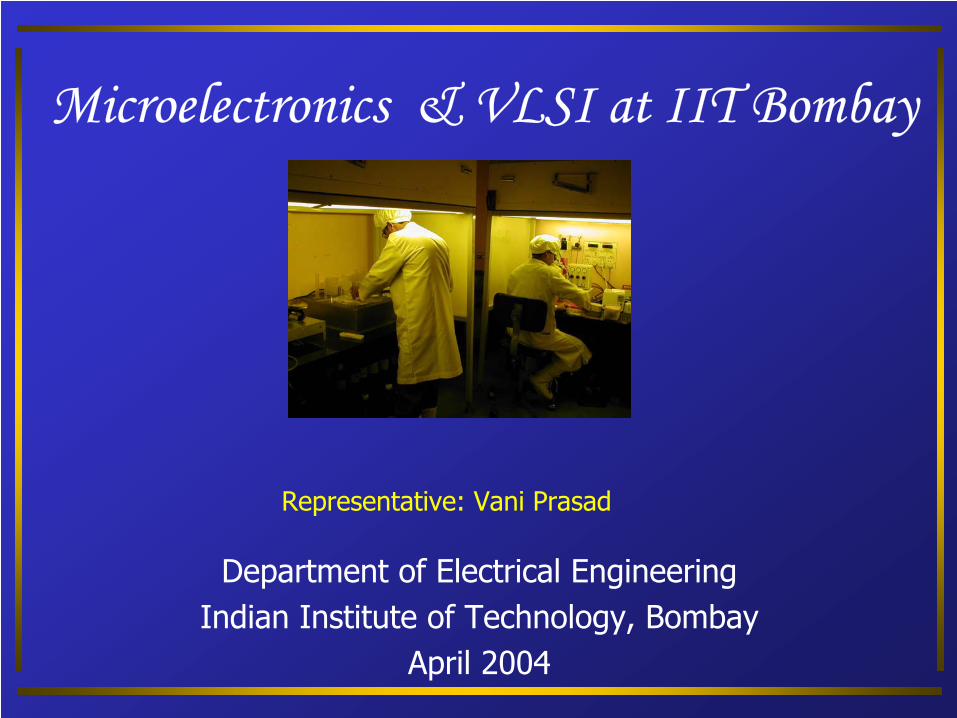
Microelectronics & VLSI at IIT Bombay
Department of Electrical EngineeringIndian Institute of Technology, Bombay
April 2004
Representative: Vani Prasad
Faculty
• P. R. Apte• A. N. Chandorkar• M. P. Desai• S. Duttagupta• B. Gadepally*• R. Lal• S. Mahapatra• H. Narayanan
• R. Parekhji* • M. B. Patil• R. Pinto• V. Ramgopal Rao• D. K. Sharma• S. D. Sherlekar*• J. Vasi
*Adjunct
Associated Faculty• A. Karandikar Elec. Engg.• D. Manjunath Elec. Engg.• H. Pillai Elec. Engg.• S. S. S. P. Rao Comp. Sci. & Engg.• S. Chakrabarty Comp. Sci. & Engg.• S. Patkar Maths• R. O. Dusane Met. Eng. & Mat. Sci.• R. Srinivasa Met. Eng. & Mat. Sci.• A. Contractor Chemistry• M. Ravikanth Chemistry• S. Mukherji Bio-medical
Areas of R & D
• Silicon CMOS physics and technology• MEMS, BioMEMS• New materials• Device modeling and simulation• VLSI design (digital, analog, mixed-mode)• VLSI CAD tool development• Interaction between VLSI technology and
design
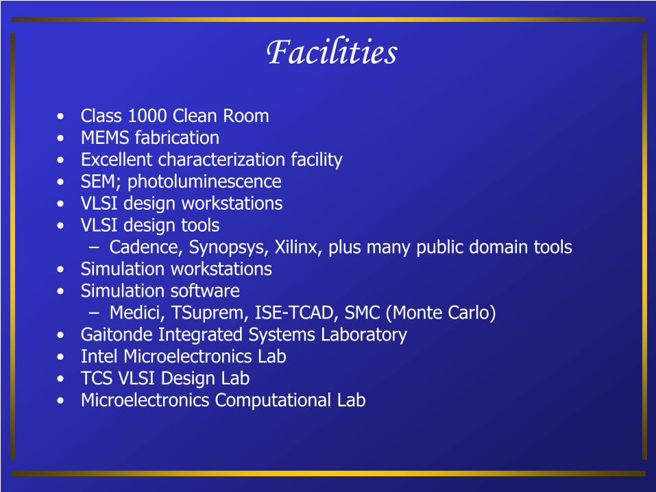
Facilities• Class 1000 Clean Room• MEMS fabrication • Excellent characterization facility• SEM; photoluminescence• VLSI design workstations• VLSI design tools
– Cadence, Synopsys, Xilinx, plus many public domain tools• Simulation workstations• Simulation software
– Medici, TSuprem, ISE-TCAD, SMC (Monte Carlo)• Gaitonde Integrated Systems Laboratory• Intel Microelectronics Lab• TCS VLSI Design Lab• Microelectronics Computational Lab

Some Ongoing Research topics:
1. Device Physics and Technology
2. Very Large Scale Integration (VLSI) Design
3. VLSI CAD
Device Physics and Technology
1) Non-Volatile Memories
• Flash Memory and SONOS• Close to an ideal memory and therefore useful for embedded
applications (BIOS, Cell phones, DigiCams)• Aim of the work is to understand the physics behind various
mechanisms and evaluate the device scalability and reliability prospects• Work involves characterization, process and device simulation• Collaboration with Agere, USA and Hitachi, Japan
Prof J. VasiProf S. MahapatraProf V. Ramgopal Rao
Deleep R. Nair (RS) (drnair@ee)P. Bharath Kumar (RS) (bharath@ee)Pradeep R. NairRavinder SharmaBhawna TomarAnupama Garg
2) Bias Temperature Instability (BTI) in MOS Devices
Characteristics of a MOS device (like Vth, Id, gm) drift gradually under the combination of high temperature and gate bias. Serious problem in analog circuits which require matched transistor pairs.Severe in PMOS under Negative Bias (NBTI) and becomes more serious with
scalingThis project aims at understanding the physics behind BTI, which is not yet fully known
Prof. J. VasiProf. V. Ramgopal RaoProf. S. Mahapatra
Neeraj K. JhaP. Bharath KumarTapas R. Dalei
3) MOS Reliability under Analog Operating Conditions
To characterise and model the degradation behaviour of analog circuits fabricated with different technologies under the CHC (Channel Hot Carrier) and NBTI (Negative Bias Temperature Instability) degradation under analog operating conditions
With the scaling of technology and the emergence of SoC (System-on-Chip) analog circuits require separate (from digital approach) reliability solutions.
Prof. V. R. RaoProf M.B. PatilProf D.K. Sharma
Neeraj K. Jha (RS) (neerajha@ee)P. S. Reddy
4) Effect of transistor scaling on mixed-signal circuit performance
Sub 100 nm devices drive the transistor cut-off frequencies in the range of RF, opening a corner for Si CMOS System-on-chip
Transistor scaling adversely affects the analog circuitperformance, more significantly on the output resistance.
It is observed from this work that channel engineering will boost the analog circuit performance making the CMOS technology suitable for mixed signal circuits.
This work is financially supported by Intel, USA.
Prof. V. Ramgopal RaoProf. Dinesh Sharma
Neeraj Jha (RS) (neerajha@ee )K. Narasimhulu (RS) (narsimha@ee )Abhishek JhaAbdul Haseeb
5) Application of look-up table approach to circuit simulation
Attractive alternative to the circuit simulation is Look-up Table (LUT) approachBasic Idea:
Extract the terminal currents and charges for a set of biases of interest and feed it to the LUT template. This template calculates the functions and derivatives w.r.t all the independent variables at any point using suitable interpolation scheme. The LUT program is implemented in SEQUEL (developed at IIT-Bombay) general purpose circuit simulator.
Prof. M.B. PatilProf. V. Ramgopal RaoProf J. Vasi
D. Vinay Kumar (RS) (vinay@ee)Saurabh N. AgarwalPalkesh Jain Abhishek Jha
6) Micro-mechanical systems (MEMS) Projects
iSens project work on hand-held heart attack sensors;Three appoaches: Cantilevers, Conducting polymers, Electrolyte-Insulator-Semiconductor (EIS) Capacitors.
Fabrication done at IITB.
* Fabrication and Characterization of Polysilicon/SU-8 Cantilevers for Biochemical Sensing – (detecting the cardiac marker)
Funding Agency: National Programme for Smart Materials, Sensors and Devices
Prof. V. Ramgopal RaoProf. R. O. Dusane
Nitin Kale (RS) (nsk@ee)
Ravi Kakkad, Naveen Bazar, Ruchin Sinha
7) Radiation-Hard CMOS Analog/Digital Design
To understand the damage caused by radiation on CMOS devices and to tolerate this damage by use of special (and novel) device/circuit/layout techniques. Some of these circuits (SRAM, high gain op-amps and variety of individual transistors) have been fabricated from TSMC in 0.35 um technology and their testing is on.
Prof J. VasiProf R. LalProf D.K. Sharma
Palkesh JainPrabha TomarTanuj KhandelwalRitesh Garg
Nano-technology project
MCIT sponsored project worth Rupees 50 crores
New processing facilities facility for making nano-structures ( a 5-storeyed bldg coming up behind EE annexe)
Many openings in this field ☺
VLSI Design and CAD
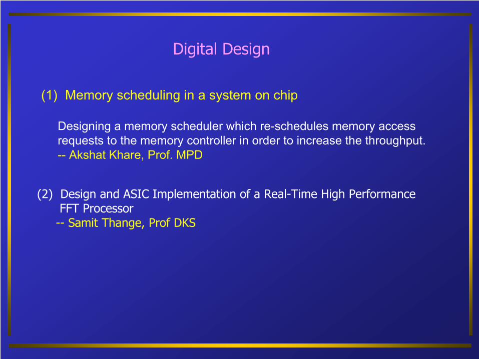
(1) Memory scheduling in a system on chip
Designing a memory scheduler which re-schedules memory access requests to the memory controller in order to increase the throughput.-- Akshat Khare, Prof. MPD
(2) Design and ASIC Implementation of a Real-Time High Performance FFT Processor
-- Samit Thange, Prof DKS
Digital Design
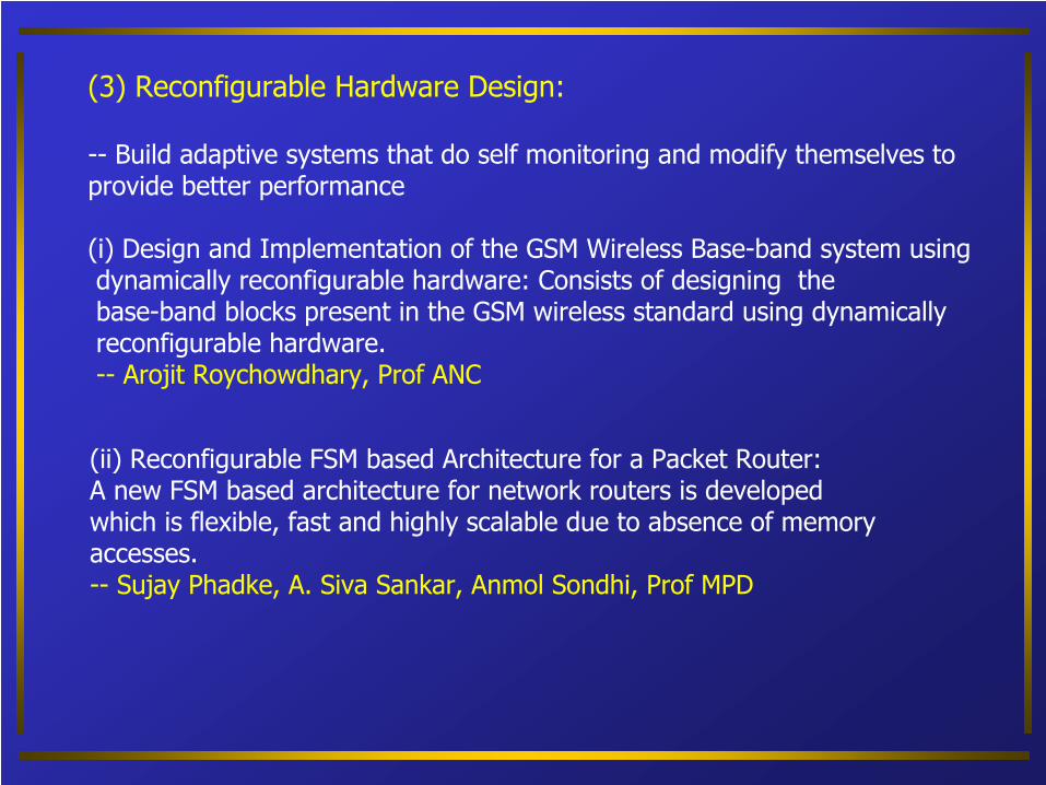
(ii) Reconfigurable FSM based Architecture for a Packet Router:A new FSM based architecture for network routers is developed which is flexible, fast and highly scalable due to absence of memory accesses.-- Sujay Phadke, A. Siva Sankar, Anmol Sondhi, Prof MPD
(3) Reconfigurable Hardware Design:
-- Build adaptive systems that do self monitoring and modify themselves toprovide better performance
(i) Design and Implementation of the GSM Wireless Base-band system using dynamically reconfigurable hardware: Consists of designing thebase-band blocks present in the GSM wireless standard using dynamically reconfigurable hardware.-- Arojit Roychowdhary, Prof ANC
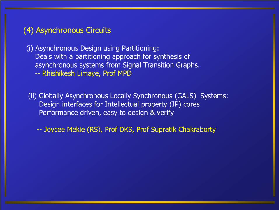
(4) Asynchronous Circuits
(i) Asynchronous Design using Partitioning:Deals with a partitioning approach for synthesis ofasynchronous systems from Signal Transition Graphs.-- Rhishikesh Limaye, Prof MPD
(ii) Globally Asynchronous Locally Synchronous (GALS) Systems:Design interfaces for Intellectual property (IP) coresPerformance driven, easy to design & verify
-- Joycee Mekie (RS), Prof DKS, Prof Supratik Chakraborty
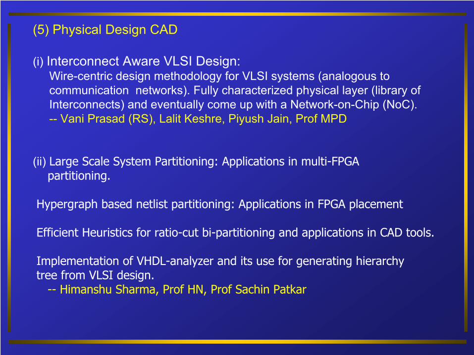
(5) Physical Design CAD
(i) Interconnect Aware VLSI Design:Wire-centric design methodology for VLSI systems (analogous to communication networks). Fully characterized physical layer (library of Interconnects) and eventually come up with a Network-on-Chip (NoC).-- Vani Prasad (RS), Lalit Keshre, Piyush Jain, Prof MPD
(ii) Large Scale System Partitioning: Applications in multi-FPGApartitioning.
Hypergraph based netlist partitioning: Applications in FPGA placement
Efficient Heuristics for ratio-cut bi-partitioning and applications in CAD tools.
Implementation of VHDL-analyzer and its use for generating hierarchy tree from VLSI design.
-- Himanshu Sharma, Prof HN, Prof Sachin Patkar
(6) Testability and Fault Simulation:
Fault Simulation on reconfigurable hardware.-- B. Kalyan Chakrabarty, Prof MPD
VLSI Computer Aided Design (CAD)
1) Algorithm to Chip: Architectural exploration in high level synthesisGenerating a specific hardware from C code
-- Hakim Raja, Prof MPD, (IT Dept – Sameer, Prof K. Arya)
2) Circuit Simulation Activities:DC Analysis of linear and non-linear circuits with Diodes, Resistors and Independent SourcesThe circuit simulator here is based upon Modified Two Graph Method of DC Analysis as well as Newton Raphson method and finds application in solution of Min-Cost Flow problem using electrical circuit analysis.-- Gaurav Trivedi (RS), Anshu Jain , Prof HN, Prof MPD
3) Circuit order reduction of VLSI interconnects (Reduction of simulation time at HF)-- Hanumant Singh Shekawat, Prof Harish Pillai
Analog and RF Design
(1) PLL Frequency Synthesizer (for ISM band range)Focus is on reducing phase noise and spurs using on-chip spiral inductors for complete integration. Synthesizer designed for transceiver application.-- Sachin Kanagude, Prof ANC
(2) Current mode low voltage low power Sigma Delta A/D converter(for base-band channel application) The focus is on reducing power.-- Brajesh Kumar, Prof ANC
High Speed Sigma-Delta converter for wide band CDMA applications-- S. Sudhakar, Prof ANC
Design of a High Performance Sigma-Delta A/D Converter:14-bits, 12.5MHz second order dual quantizer Sigma-Delta ADC.
-- Neeraj Shrivastava, Prof DKS
(3) Dual-Band RF transmitter and receiver design:Designing a transmitter and receiver IC that can work with 802.11a and 802.11b bands concurrently. Test chip fabricated for some of the RF blocksin the TX, RX.-- Rittu Sachdev, Saumitra Singh, Prof DKS
(5) Tunable Inductors for RF applications:Optimizing the performance of RF front end circuits by adjusting the center frequency of a band pass filter and tuning the oscillatorfrequency of a VCO -- N. Bheema Rao (RS), Prof ANC
(4) Design of 2.4-GHz RF Transmitter:Design a direct conversion RF transmitter for remote applications -- N. Nagaraju, Prof DKS

Interaction between technology and VLSI design
Possibility of Using DTMOS to Solve the Voltage Scaling Problem
DTMOS: Increase speed using “forward” body bias without increasing leakage
Areas of work:Body biasing schemes to offset the effect of body’s parasitic resistance and
capacitanceDevice redesign taking body’s parasitic components into accountConsidering the effect of body’s parasitic components in circuit design
-- B. Anand (RS), Prof MPD, Prof VRR
Let’s ponder…
• Most of the device/technology projects are funded by industries.
• No sponsorship for design projects!
• Need more faculty in VLSI Design/CAD
• uE group or Device Group?
Need interaction with the industries
So what r we looking for?
More feedback from faculty group projects
Acknowledgement
PhDs, Mtechs, DDs and BTechs of uE group


Challenges in a "synchronous" SoC design
a. Different Functional blocks on a single chipb. Clock Distributionc. Time to market (TTM) d. Performance issues e. Verification issues
Solution GALS
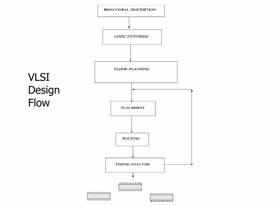
VLSI DesignFlow
Recommended