INSTITUTE of APPLIED PHYSICSFriedrich-Schiller University Jena
U.D. U.D. ZeitnerZeitnerFraunhofer Institut fFraunhofer Institut füür Angewandte Optik und Feinmechanikr Angewandte Optik und Feinmechanik
JenaJena
Micro- and Nano-Technology...... for Optics
3.1 Layer Deposition

INSTITUTE of APPLIED PHYSICSFriedrich-Schiller University Jena
2. Resist exposure with e-beam lithography
Typical Micro-Structuring Process
3. Resist development
4. Chromium etching (RIE)
5. Deep etching into substrate (ICP)
resist
Cr-layer
SiO2-Substrate
radiation1. Substrate coating

INSTITUTE of APPLIED PHYSICSFriedrich-Schiller University Jena
Thin Film Deposition Techniques
layer deposition
from vapor / gaseous phase from liquid phase
CVD PVD
thermal activation
plasma activation
sputtering thermal evaporation
• dip coating• spray coating• spin coating• galvanic layer
deposition

INSTITUTE of APPLIED PHYSICSFriedrich-Schiller University Jena
CVD – Thermal Activation

INSTITUTE of APPLIED PHYSICSFriedrich-Schiller University Jena
CVD – Plasma Enhanced (PECVD)

INSTITUTE of APPLIED PHYSICSFriedrich-Schiller University Jena
CVD – Plasma Enhanced (PECVD)
anode
cathode
HF-electrode
ground
reactor chamber
gas inlet
gas outlet
substrate
plasma

INSTITUTE of APPLIED PHYSICSFriedrich-Schiller University Jena
PVD Techniques
Source: Donald M. Mattox, SVC Educational Guides to Vacuum Coating Processing

INSTITUTE of APPLIED PHYSICSFriedrich-Schiller University Jena
Sputtering
anode
cathode
HF-electrode
ground
reactor chamber
gas inlet
gas outlet
substrate
plasma
target(layer material)
target atom

INSTITUTE of APPLIED PHYSICSFriedrich-Schiller University Jena
Thermal Evaporation
typical evaporation sources

INSTITUTE of APPLIED PHYSICSFriedrich-Schiller University Jena
Electron Beam Evaporation

INSTITUTE of APPLIED PHYSICSFriedrich-Schiller University Jena
Particle movement in vacuum
pressure [Pa]
mea
n fr
ee p
ath
leng
th [m
]atmospheric pressure: 101 kPa ≈ 105 Pa
INSTITUTE of APPLIED PHYSICSFriedrich-Schiller University Jena
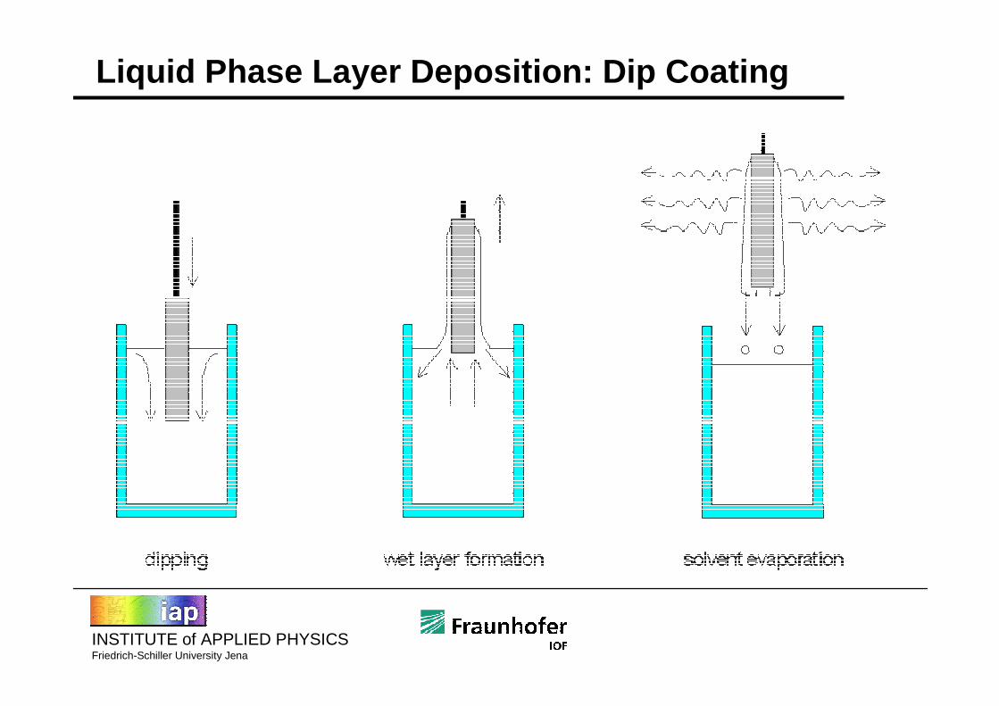
Liquid Phase Layer Deposition: Dip Coating

INSTITUTE of APPLIED PHYSICSFriedrich-Schiller University Jena
Liquid Phase Layer Deposition: Spin Coating
Recommended