Document No.: M-W2539AE-14.0
ANRITSU CORPORATION
MG3700A Vector Signal Generator
Operation Manual (Standard Waveform Pattern)
14th Edition
• For safety and warning information, please read this manual before attempting to use the equipment.
• Additional safety and warning information is provided within the MG3700A Vector Signal Generator Operation Manual (Mainframe). Please also refer to this document before using the equipment.
• Keep this manual with the equipment.
ii
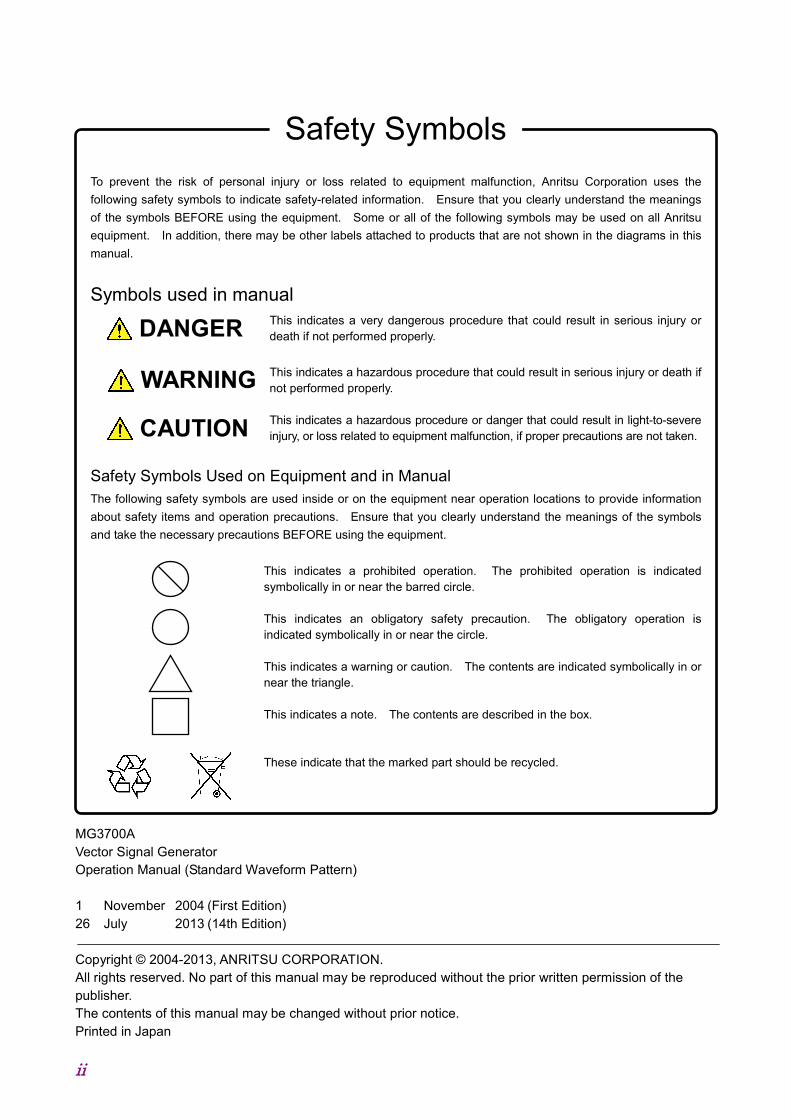
Safety Symbols To prevent the risk of personal injury or loss related to equipment malfunction, Anritsu Corporation uses the following safety symbols to indicate safety-related information. Ensure that you clearly understand the meanings of the symbols BEFORE using the equipment. Some or all of the following symbols may be used on all Anritsu equipment. In addition, there may be other labels attached to products that are not shown in the diagrams in this manual.
Symbols used in manual This indicates a very dangerous procedure that could result in serious injury or death if not performed properly.
This indicates a hazardous procedure that could result in serious injury or death if not performed properly. This indicates a hazardous procedure or danger that could result in light-to-severe injury, or loss related to equipment malfunction, if proper precautions are not taken.
Safety Symbols Used on Equipment and in Manual The following safety symbols are used inside or on the equipment near operation locations to provide information about safety items and operation precautions. Ensure that you clearly understand the meanings of the symbols and take the necessary precautions BEFORE using the equipment.
This indicates a prohibited operation. The prohibited operation is indicated symbolically in or near the barred circle.
This indicates an obligatory safety precaution. The obligatory operation is
indicated symbolically in or near the circle. This indicates a warning or caution. The contents are indicated symbolically in or
near the triangle. This indicates a note. The contents are described in the box. These indicate that the marked part should be recycled.
MG3700A Vector Signal Generator Operation Manual (Standard Waveform Pattern) 1 November 2004 (First Edition) 26 July 2013 (14th Edition) Copyright © 2004-2013, ANRITSU CORPORATION. All rights reserved. No part of this manual may be reproduced without the prior written permission of the publisher. The contents of this manual may be changed without prior notice. Printed in Japan
DANGER
WARNING
CAUTION
iii
Equipment Certificate Anritsu Corporation guarantees that this equipment was inspected at shipment and meets the published specifications.
Anritsu Warranty • During the warranty period, Anritsu Corporation will repair or exchange this
software free-of-charge if it proves defective when used as described in the operation manual.
• The warranty period is 6 months from the purchase date. • The warranty period after repair or exchange will remain 6 months from
the original purchase date, or 30 days from the date of repair or exchange, depending on whichever is longer.
• This warranty does not cover damage to this software caused by Acts of God, natural disasters, and misuse or mishandling by the customer.
In addition, this warranty is valid only for the original equipment purchaser. It is not transferable if the equipment is resold. Anritsu Corporation shall assume no liability for injury or financial loss of the customer due to the use of or a failure to be able to use this equipment.
Anritsu Corporation Contact In the event that this equipment malfunctions, contact an Anritsu Service and Sales office. Contact information can be found on the last page of the printed version of this manual, and is available in a separate file on the CD version.
iv
Notes On Export Management This product and its manuals may require an Export License/Approval by the Government of the product's country of origin for re-export from your country. Before re-exporting the product or manuals, please contact us to confirm whether they are export-controlled items or not. When you dispose of export-controlled items, the products/manuals need to be broken/shredded so as not to be unlawfully used for military purpose.
Trademark and Registered Trademark IQproducerTM is a registered trademark of Anritsu Corporation.
v
Software End-User License Agreement (EULA) Please read this Software End-User License Agreement (hereafter this EULA) carefully before using (includes executing, copying, registering, etc.) this software (includes programs, databases, scenarios, etc., used to operate, set, etc., Anritsu electronic equipment). By reading this EULA and using this software, you are agreeing to be bound by the terms of its contents and Anritsu Corporation (hereafter Anritsu) hereby grants you the right to use this Software with the Anritsu-specified equipment (hereafter Equipment) for the purposes set out in this EULA. 1. Grant of License and Limitations
1. Regardless of whether this Software was purchased from or provided free-of-charge by Anritsu, you agree not to rent, lease, lend, or otherwise distribute this Software to third parties and further agree not to disassemble, recompile, reverse engineer, modify, or create derivative works of this Software.
2. You may make one copy of this Software for backup purposes only.
3. You are not permitted to reverse engineer this software.
4. This EULA allows you to install one copy of this Software on one piece of Equipment.
2. Disclaimers To the extent not prohibited by law, in no
event shall Anritsu be liable for personal injury, or any incidental, special, indirect or consequential damages whatsoever, including, without limitation, damages for loss of profits, loss of data, business interruption or any other commercial damages or losses, arising out of or related to your use or inability to use this Software.
3. Limitation of Liability a. If a fault (bug) is discovered in this Software,
preventing operation as described in the operation manual or specifications whether or not the customer uses this software as described in the manual, Anritsu shall at its own discretion, fix the bug, or exchange the software, or suggest a workaround, free-of-charge. However, notwithstanding the above, the following items shall be excluded from repair and warranty.
i) If this Software is deemed to be used for purposes not described in the operation manual or specifications.
ii) If this Software is used in conjunction with other non-Anritsu-approved software.
iii) Recovery of lost or damaged data. iv) If this Software or the Equipment has been
modified, repaired, or otherwise altered without Anritsu's prior approval.
v) For any other reasons out of Anritsu's direct control and responsibility, such as but not limited to, natural disasters, software virus infections, etc.
b. Expenses incurred for transport, hotel, daily allowance, etc., for on-site repairs by Anritsu engineers necessitated by the above faults shall be borne by you.
c. The warranty period for faults listed in article 3a above covered by this EULA shall be either 6 months from the date of purchase of this Software or 30 days after the date of repair, whichever is longer.
vi
4. Export Restrictions You may not use or otherwise export or
re-export directly or indirectly this Software except as authorized by Japanese and United States law. In particular, this software may not be exported or re-exported (a) into any Japanese or US embargoed countries or (b) to anyone on the Japanese or US Treasury Department's list of Specially Designated Nationals or the US Department of Commerce Denied Persons List or Entity List. By using this Software, you warrant that you are not located in any such country or on any such list. You also agree that you will not use this Software for any purposes prohibited by Japanese and US law, including, without limitation, the development, design and manufacture or production of missiles or nuclear, chemical or biological weapons of mass destruction.
5. Termination Anritsu shall deem this EULA terminated if
you violate any conditions described herein. This EULA shall also be terminated if the conditions herein cannot be continued for any good reason, such as violation of copyrights, patents, or other laws and ordinances.
6. Reparations If Anritsu suffers any loss, financial or
otherwise, due to your violation of the terms of this EULA, Anritsu shall have the right to seek proportional damages from you.
7. Responsibility after Termination Upon termination of this EULA in
accordance with item 5, you shall cease all use of this Software immediately and shall as directed by Anritsu either destroy or return this Software and any backup copies, full or partial, to Anritsu.
8. Dispute Resolution If matters of dispute or items not covered by
this EULA arise, they shall be resolved by negotiations in good faith between you and Anritsu.
9. Court of Jurisdiction This EULA shall be interpreted in
accordance with Japanese law and any disputes that cannot be resolved by negotiation described in Article 8 shall be settled by the Japanese courts.
vii
Cautions against computer virus infection • Copying files and data Only files that have been provided directly from Anritsu or generated
using Anritsu equipment should be copied to the instrument. All other required files should be transferred by means of USB or
CompactFlash media after undergoing a thorough virus check. • Adding software Do not download or install software that has not been specifically
recommended or licensed by Anritsu. • Network connections Ensure that the network has sufficient anti-virus security protection in
place.

viii
I
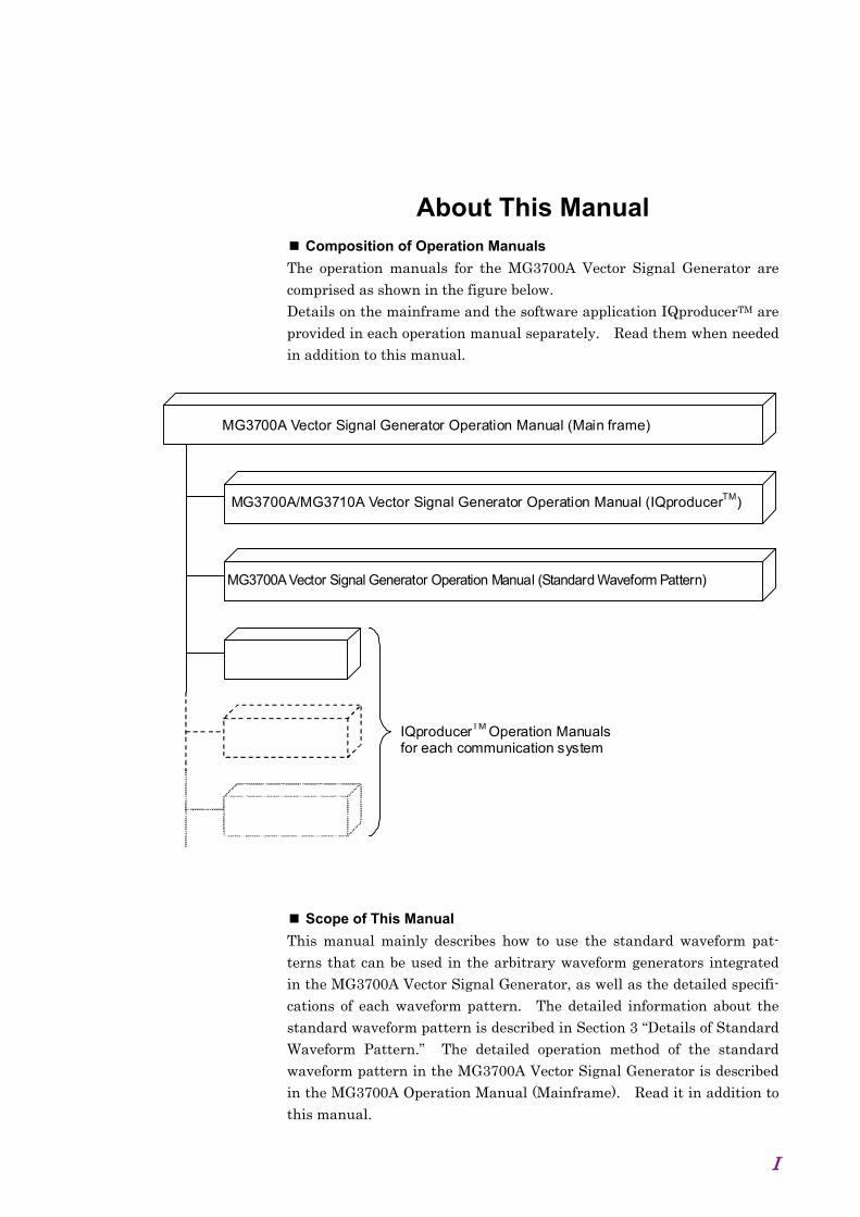
About This Manual Composition of Operation Manuals
The operation manuals for the MG3700A Vector Signal Generator are comprised as shown in the figure below. Details on the mainframe and the software application IQproducerTM are provided in each operation manual separately. Read them when needed in addition to this manual.
MG3700A Vector Signal Generator Operation Manual (Main frame)
MG3700A/MG3710A Vector Signal Generator Operation Manual (IQproducerTM)
MG3700A Vector Signal Generator Operation Manual (Standard Waveform Pattern)
IQproducerTM Operation Manuals for each communication system
Scope of This Manual
This manual mainly describes how to use the standard waveform pat-terns that can be used in the arbitrary waveform generators integrated in the MG3700A Vector Signal Generator, as well as the detailed specifi-cations of each waveform pattern. The detailed information about the standard waveform pattern is described in Section 3 “Details of Standard Waveform Pattern.” The detailed operation method of the standard waveform pattern in the MG3700A Vector Signal Generator is described in the MG3700A Operation Manual (Mainframe). Read it in addition to this manual.
II.
Table of Contents
About This Manual........................................ I
Section 1 Outline ....................................... 1-1 1.1 Outline of Product ......................................................... 1-2
Section 2 How to Use Standard Waveform
Pattern ....................................... 2-1 2.1 How to Use Standard Waveform Pattern ...................... 2-2
2.2 Configuration of Standard Waveform Pattern
Package ........................................................................ 2-4
2.3 Output Level Range of Standard Waveform Pattern .... 2-5
Section 3 Details of Standard Waveform
Pattern ....................................... 3-1 3.1 W-CDMA Waveform Pattern ......................................... 3-3 3.2 PDC Waveform Pattern ................................................ 3-58 3.3 PDC PACKET Waveform Pattern ................................. 3-62 3.4 PHS Waveform Pattern ................................................. 3-65 3.5 GSM Waveform Pattern ................................................ 3-69 3.6 CDMA2000 1X Waveform Pattern ................................ 3-74 3.7 CDMA2000 1xEV-DO Waveform Pattern ..................... 3-91 3.8 WLAN Waveform Pattern.............................................. 3-103 3.9 AWGN Waveform Pattern ............................................. 3-110 3.10 Digital Broadcast Waveform Pattern ............................. 3-111 3.11 Bluetooth® Waveform Pattern ....................................... 3-117 3.12 GPS Waveform Pattern ................................................ 3-128
Index .......................................................... Index-1

Section 1 Outline
1-1
This section provides an outline of the standard waveform pattern for the
MG3700A Vector Signal Generator.
1.1 Outline of Product ...................................................... 1-2
Section 1 Outline
1-2.
1.1 Outline of ProductThe standard waveform pattern for the MG3700A Vector SignalGenerator (hereafter referred to as “standard waveform pattern”) consistsof waveform patterns (see Note) that are used in a wide range ofapplications from research and development to manufacturing of thesystems, devices, and equipment in the field of digital mobile
communications.
The standard waveform pattern can be used in the MG3700A VectorSignal Generator (hereafter referred to as “MG3700A”) that integrates anarbitrary waveform generator.
Note:The waveform pattern described here indicates arbitrary waveformdata used for supporting various radio communication systems thatcan be used by the arbitrary waveform generator integrated in theMG3700A.The waveform pattern consists of two files: arbitrary waveform fileand waveform information file. The arbitrary waveform file is abinary-format file with the extension “.wvd”. The waveforminformation file is a text-format file with the extension “.wvi”, usedto control arbitrary waveform data and set the hardware forwaveform data output.
Waveform patterns that use two memories as shown below can beoperated easily by using a combination file that defines a combination oftwo waveform patterns to be loaded from memories A and B, and sets the
output level for memories.
• A waveform pattern that uses two memories to output one signal, suchas a W-CDMA downlink desired signal
• A waveform pattern that is generated by adding two signals, such as adesired wave used for receiver evaluation and an interference signal orAWGN, using the baseband
Section 2 How to Use Standard Waveform Pattern
2-1
This section describes how to use the standard waveform pattern and the
configuration of the standard waveform pattern package.
2.1 How to Use Standard Waveform Pattern .................. 2-22.2 Configuration of Standard Waveform Pattern
Package..................................................................... 2-42.3 Output Level Range of Standard Waveform Pattern. 2-5
Section 2 How to Use Standard Waveform Pattern
2-2
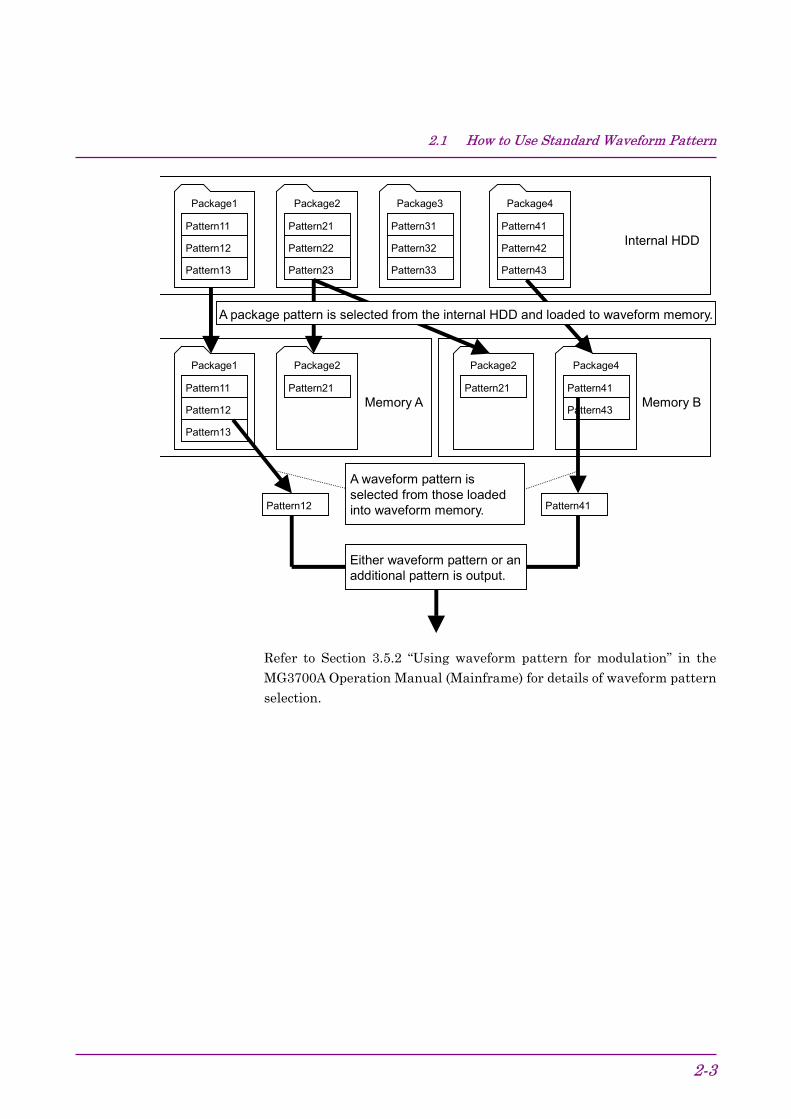
2.1 How to Use Standard Waveform PatternThe standard waveform pattern is shipped being stored in the internalhard disk of the MG3700A.The waveform pattern stored in the internal hard disk is reproduced bythe arbitrary waveform generator integrated in the MG3700A, and usedto perform vector modulation. The waveform patterns are classified bycommunication type and stored in a folder. This folder is called as apackage, and the standard waveform patterns classified bycommunication type are stored in each package with the correspondingcommunication system name. When reproducing a waveform pattern, itis necessary first to load the package pattern stored in the internal harddisk to a waveform memory in the MG3700A. The MG3700A has twowaveform memories A and B that have the I/Q 2-channel configuration.Waveform patterns are loaded to either or both of these two waveform
memories.
Then, select a waveform pattern to be output from the patterns loadedinto the waveform memory. Only one waveform pattern can be selectedfrom each memory. A waveform pattern selected from the waveformmemory A or B, or an additional waveform generated by adding twowaveform patterns selected from both waveform memories A and B isoutput.
2.1 How to Use Standard Waveform Pattern
2-3
Pattern11
Pattern12
Pattern13
Package1 Package2
Pattern21
Pattern22
Pattern23
Internal HDD
Memory B
Package3
Pattern31
Pattern32
Pattern33
Pattern11
Pattern12
Pattern13
Package1
Package4
Pattern41
Pattern42
Pattern43
Package2
Pattern21
Package4
Pattern41
Pattern43
Package2
Pattern21
A package pattern is selected from the internal HDD and loaded to waveform memory.
Pattern12 Pattern41
Memory A
A waveform pattern is selected from those loaded into waveform memory.
Either waveform pattern or an additional pattern is output.
Refer to Section 3.5.2 “Using waveform pattern for modulation” in theMG3700A Operation Manual (Mainframe) for details of waveform patternselection.
Section 2 How to Use Standard Waveform Pattern
2-4
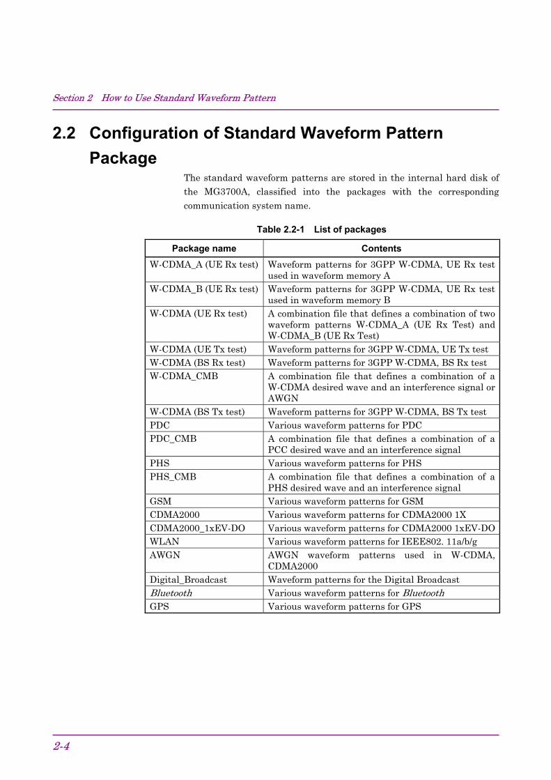
2.2 Configuration of Standard Waveform PatternPackage
The standard waveform patterns are stored in the internal hard disk ofthe MG3700A, classified into the packages with the corresponding
communication system name.
Table 2.2-1 List of packages
Package name ContentsW-CDMA_A (UE Rx test) Waveform patterns for 3GPP W-CDMA, UE Rx test
used in waveform memory AW-CDMA_B (UE Rx test) Waveform patterns for 3GPP W-CDMA, UE Rx test
used in waveform memory BW-CDMA (UE Rx test) A combination file that defines a combination of two
waveform patterns W-CDMA_A (UE Rx Test) andW-CDMA_B (UE Rx Test)
W-CDMA (UE Tx test) Waveform patterns for 3GPP W-CDMA, UE Tx testW-CDMA (BS Rx test) Waveform patterns for 3GPP W-CDMA, BS Rx testW-CDMA_CMB A combination file that defines a combination of a
W-CDMA desired wave and an interference signal orAWGN
W-CDMA (BS Tx test) Waveform patterns for 3GPP W-CDMA, BS Tx testPDC Various waveform patterns for PDCPDC_CMB A combination file that defines a combination of a
PCC desired wave and an interference signalPHS Various waveform patterns for PHSPHS_CMB A combination file that defines a combination of a
PHS desired wave and an interference signalGSM Various waveform patterns for GSMCDMA2000 Various waveform patterns for CDMA2000 1XCDMA2000_1xEV-DO Various waveform patterns for CDMA2000 1xEV-DOWLAN Various waveform patterns for IEEE802. 11a/b/gAWGN AWGN waveform patterns used in W-CDMA,
CDMA2000Digital_Broadcast Waveform patterns for the Digital BroadcastBluetooth Various waveform patterns for BluetoothGPS Various waveform patterns for GPS
2.3 Output Level Range of Standard Waveform Pattern
2-5
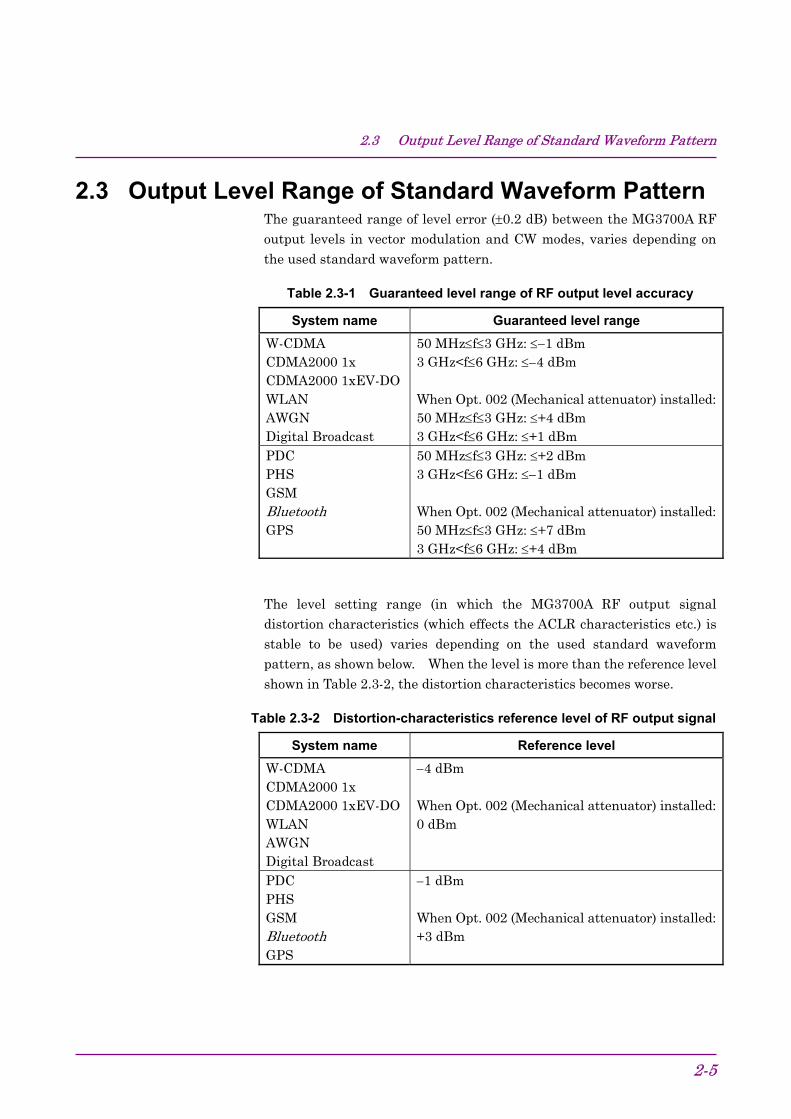
2.3 Output Level Range of Standard Waveform PatternThe guaranteed range of level error (±0.2 dB) between the MG3700A RFoutput levels in vector modulation and CW modes, varies depending on
the used standard waveform pattern.
Table 2.3-1 Guaranteed level range of RF output level accuracy
System name Guaranteed level rangeW-CDMACDMA2000 1xCDMA2000 1xEV-DOWLANAWGNDigital Broadcast
50 MHz≤f≤3 GHz: ≤−1 dBm3 GHz<f≤6 GHz: ≤−4 dBm
When Opt. 002 (Mechanical attenuator) installed:50 MHz≤f≤3 GHz: ≤+4 dBm3 GHz<f≤6 GHz: ≤+1 dBm
PDCPHSGSMBluetoothGPS
50 MHz≤f≤3 GHz: ≤+2 dBm3 GHz<f≤6 GHz: ≤−1 dBm
When Opt. 002 (Mechanical attenuator) installed:50 MHz≤f≤3 GHz: ≤+7 dBm3 GHz<f≤6 GHz: ≤+4 dBm
The level setting range (in which the MG3700A RF output signaldistortion characteristics (which effects the ACLR characteristics etc.) isstable to be used) varies depending on the used standard waveformpattern, as shown below. When the level is more than the reference level
shown in Table 2.3-2, the distortion characteristics becomes worse.
Table 2.3-2 Distortion-characteristics reference level of RF output signal
System name Reference levelW-CDMACDMA2000 1xCDMA2000 1xEV-DOWLANAWGNDigital Broadcast
−4 dBm
When Opt. 002 (Mechanical attenuator) installed:0 dBm
PDCPHSGSMBluetoothGPS
−1 dBm
When Opt. 002 (Mechanical attenuator) installed:+3 dBm

Section 2 How to Use Standard Waveform Pattern
2-6.
Section 3 Details of Standard Waveform Pattern
3-1
This section describes each standard waveform pattern in detail.
3.1 W-CDMA Waveform Pattern ......................................... 3-3 3.1.1 UL_RMCxxxkbps .............................................. 3-9 3.1.2 UL_AMR_TFCSx/UL_ISDN/UL_64kbps
_Packet ........................................................... 3-20 3.1.3 UL_Interferer .................................................. 3-27 3.1.4 DL_RMCxxxkbps ............................................ 3-28 3.1.5 DL_AMR_TFCSx/DL_ISDN/DL_384kbps
_Packet ........................................................... 3-38 3.1.6 DL_Interferer .................................................. 3-44 3.1.7 TestModel_x_xxDPCH ................................... 3-46 3.1.8 TestModel_5_xDPCH ..................................... 3-52 3.1.9 TestModel_5_xHSPDSCH ............................. 3-52 3.1.10 TestModel_6_xHSPDSCH ............................. 3-55
3.2 PDC Waveform Pattern .............................................. 3-58 3.2.1 Frame configuration ........................................ 3-60 3.2.2 Slot configuration ............................................ 3-61
3.3 PDC PACKET Waveform Pattern ............................... 3-62 3.3.1 Frame configuration ........................................ 3-63 3.3.2 Slot configuration ............................................ 3-64
3.4 PHS Waveform Pattern .............................................. 3-65 3.4.1 Frame configuration ........................................ 3-67 3.4.2 Slot configuration ............................................ 3-68
3.5 GSM Waveform Pattern .............................................. 3-69 3.5.1 Details of each pattern.................................... 3-70 3.5.2 Frame configuration ........................................ 3-71 3.5.3 Slot configuration ............................................ 3-72
3.6 CDMA2000 1X Waveform Pattern .............................. 3-74 3.6.1 1xRTT Reverse RC1 (RVS_RC1_FCH) ......... 3-75 3.6.2 1xRTT Reverse RC2 (RVS_RC2_FCH) ......... 3-77 3.6.3 1xRTT Reverse RC3 (1) (RVS_RC3_FCH) ... 3-79 3.6.4 1xRTT Reverse RC3 (2)
(RVS_RC3_FCH_SCH).................................. 3-81 3.6.5 1xRTT Reverse RC3 (3)
(RVS_RC3_DCCH) ........................................ 3-83 3.6.6 1xRTT Reverse RC4 (RVS_RC4_FCH) ......... 3-85 3.6.7 1xRTT Forward RC1, 2
(FWD_RC1-2 9channel) ................................. 3-87 3.6.8 1xRTT Forward RC3, 4, 5
(FWD_RC3-5 9channel) ................................. 3-89 3.7 CDMA2000 1xEV-DO Waveform Pattern ................... 3-91
Section 3 Details of Standard Waveform Pattern
3-2
3.7.1 1xEV-DO forward (excluding FWD_Idle)........ 3-94 3.7.2 1xEV-DO reverse ........................................... 3-99 3.7.3 1xEV-DO forward idle slot ............................ 3-102
3.8 WLAN Waveform Pattern ......................................... 3-103 3.8.1 IEEE802.11a ................................................ 3-106 3.8.2 IEEE802.11b ................................................ 3-108 3.8.3 IEEE802.11g ................................................ 3-109
3.9 AWGN Waveform Pattern ......................................... 3-110 3.10 Digital Broadcast Waveform Pattern......................... 3-111
3.10.1 Frame configuration ...................................... 3-114 3.11 Bluetooth® Waveform Pattern ................................... 3-117
3.11.1 Packet configuration for Basic Rate (BR) ..... 3-120 3.11.2 Packet configuration for Enhanced Data Rate
(EDR) ............................................................ 3-123 3.11.3 Packet configuration for BLE ........................ 3-125 3.11.4 Dirty Transmitter Signal ................................ 3-127
3.12 GPS Waveform Pattern ............................................ 3-128 3.12.1 Waveform format .......................................... 3-130
3.1 W-CDMA Waveform Pattern
3-3
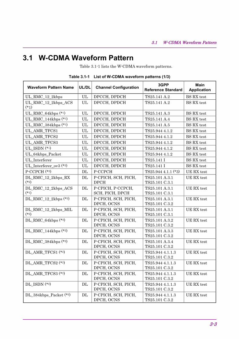
3.1 W-CDMA Waveform Pattern Table 3.1-1 lists the W-CDMA waveform patterns.
Table 3.1-1 List of W-CDMA waveform patterns (1/3)
Waveform Pattern Name UL/DL Channel Configuration 3GPP Reference Standard
Main Application
UL_RMC_12_2kbps UL DPCCH, DPDCH TS25.141 A.2 BS RX test UL_RMC_12_2kbps_ACS (*1)
UL DPCCH, DPDCH TS25.141 A.2 BS RX test
UL_RMC_64kbps (*1) UL DPCCH, DPDCH TS25.141 A.3 BS RX test UL_RMC_144kbps (*1) UL DPCCH, DPDCH TS25.141 A.4 BS RX test UL_RMC_384kbps (*1) UL DPCCH, DPDCH TS25.141 A.5 BS RX test UL_AMR_TFCS1 UL DPCCH, DPDCH TS25.944 4.1.2 BS RX test UL_AMR_TFCS2 UL DPCCH, DPDCH TS25.944 4.1.2 BS RX test UL_AMR_TFCS3 UL DPCCH, DPDCH TS25.944 4.1.2 BS RX test UL_ISDN (*1) UL DPCCH, DPDCH TS25.944 4.1.2 BS RX test UL_64kbps_Packet UL DPCCH, DPDCH TS25.944 4.1.2 BS RX test UL_Interferer UL DPCCH, DPDCH TS25.141 I BS RX test UL_Interferer_ov3 (*2) UL DPCCH, DPDCH TS25.141 I BS RX test P-CCPCH (*2) DL P-CCPCH TS25.944 4.1.1 (*3) UE RX test DL_RMC_12_2kbps_RX (*2)
DL P-CPICH, SCH, PICH, DPCH
TS25.101 A.3.1 TS25.101 C.3.1
UE RX test
DL_RMC_12_2kbps_ACS (*1)
DL P-CPICH, P-CCPCH, SCH, PICH, DPCH
TS25.101 A.3.1 TS25.101 C.3.1
UE RX test
DL_RMC_12_2kbps (*2) DL P-CPICH, SCH, PICH, DPCH, OCNS
TS25.101 A.3.1 TS25.101 C.3.2
UE RX test
DL_RMC_12_2kbps_MIL (*2)
DL P-CPICH, SCH, PICH, DPCH, OCNS
TS25.101 A.3.1 TS25.101 C.3.1
UE RX test
DL_RMC_64kbps (*2) DL P-CPICH, SCH, PICH, DPCH, OCNS
TS25.101 A.3.2 TS25.101 C.3.2
UE RX test
DL_RMC_144kbps (*2) DL P-CPICH, SCH, PICH, DPCH, OCNS
TS25.101 A.3.3 TS25.101 C.3.2
UE RX test
DL_RMC_384kbps (*2) DL P-CPICH, SCH, PICH, DPCH, OCNS
TS25.101 A.3.4 TS25.101 C.3.2
UE RX test
DL_AMR_TFCS1 (*2) DL P-CPICH, SCH, PICH, DPCH, OCNS
TS25.944 4.1.1.3 TS25.101 C.3.2
UE RX test
DL_AMR_TFCS2 (*2) DL P-CPICH, SCH, PICH, DPCH, OCNS
TS25.944 4.1.1.3 TS25.101 C.3.2
UE RX test
DL_AMR_TFCS3 (*2) DL P-CPICH, SCH, PICH, DPCH, OCNS
TS25.944 4.1.1.3 TS25.101 C.3.2
UE RX test
DL_ISDN (*2) DL P-CPICH, SCH, PICH, DPCH, OCNS
TS25.944 4.1.1.3 TS25.101 C.3.2
UE RX test
DL_384kbps_Packet (*2) DL P-CPICH, SCH, PICH, DPCH, OCNS
TS25.944 4.1.1.3 TS25.101 C.3.2
UE RX test
Section 3 Details of Standard Waveform Pattern
3-4
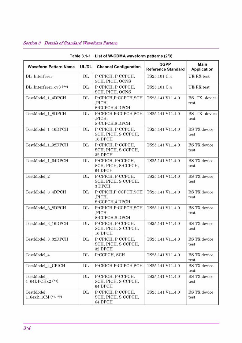
Table 3.1-1 List of W-CDMA waveform patterns (2/3)
Waveform Pattern Name UL/DL Channel Configuration 3GPP Reference Standard
Main Application
DL_Interferer DL P-CPICH, P-CCPCH, SCH, PICH, OCNS
TS25.101 C.4 UE RX test
DL_Interferer_ov3 (*6) DL P-CPICH, P-CCPCH, SCH, PICH, OCNS
TS25.101 C.4 UE RX test
TestModel_1_4DPCH DL P-CPICH,P-CCPCH,SCH,PICH, S-CCPCH,4 DPCH
TS25.141 V11.4.0 BS TX device test
TestModel_1_8DPCH DL P-CPICH,P-CCPCH,SCH,PICH, S-CCPCH,8 DPCH
TS25.141 V11.4.0 BS TX device test
TestModel_1_16DPCH DL P-CPICH, P-CCPCH, SCH, PICH, S-CCPCH, 16 DPCH
TS25.141 V11.4.0 BS TX device test
TestModel_1_32DPCH DL P-CPICH, P-CCPCH, SCH, PICH, S-CCPCH, 32 DPCH
TS25.141 V11.4.0 BS TX device test
TestModel_1_64DPCH DL P-CPICH, P-CCPCH, SCH, PICH, S-CCPCH, 64 DPCH
TS25.141 V11.4.0 BS TX device test
TestModel_2 DL P-CPICH, P-CCPCH, SCH, PICH, S-CCPCH, 3 DPCH
TS25.141 V11.4.0 BS TX device test
TestModel_3_4DPCH DL P-CPICH,P-CCPCH,SCH,PICH, S-CCPCH,4 DPCH
TS25.141 V11.4.0 BS TX device test
TestModel_3_8DPCH DL P-CPICH,P-CCPCH,SCH,PICH, S-CCPCH,8 DPCH
TS25.141 V11.4.0 BS TX device test
TestModel_3_16DPCH DL P-CPICH, P-CCPCH, SCH, PICH, S-CCPCH, 16 DPCH
TS25.141 V11.4.0 BS TX device test
TestModel_3_32DPCH DL P-CPICH, P-CCPCH, SCH, PICH, S-CCPCH, 32 DPCH
TS25.141 V11.4.0 BS TX device test
TestModel_4 DL P-CCPCH, SCH TS25.141 V11.4.0 BS TX device test
TestModel_4_CPICH DL P-CPICH,P-CCPCH,SCH TS25.141 V11.4.0 BS TX device test
TestModel_ 1_64DPCHx2 (*4)
DL P-CPICH, P-CCPCH, SCH, PICH, S-CCPCH, 64 DPCH
TS25.141 V11.4.0 BS TX device test
TestModel_ 1_64x2_10M (*4, *5)
DL P-CPICH, P-CCPCH, SCH, PICH, S-CCPCH, 64 DPCH
TS25.141 V11.4.0 BS TX device test
3.1 W-CDMA Waveform Pattern
3-5
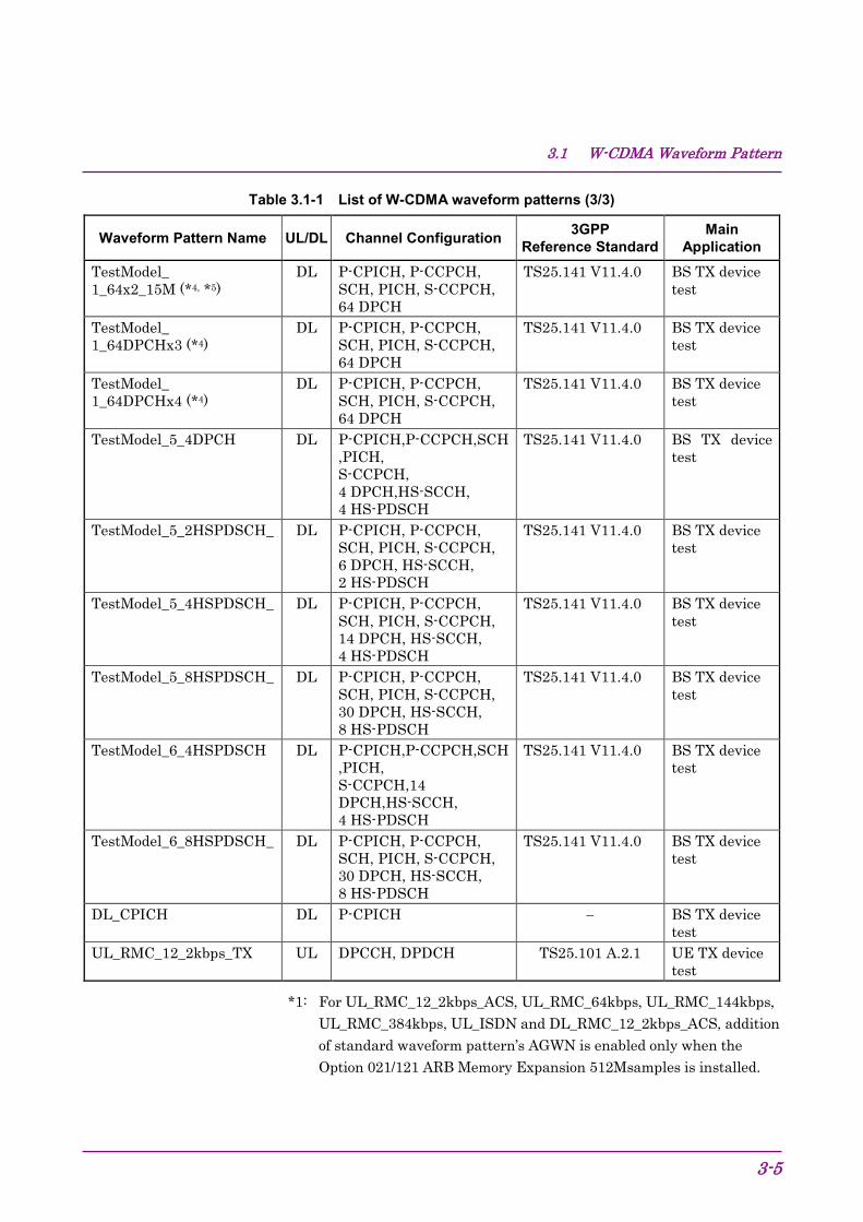
Table 3.1-1 List of W-CDMA waveform patterns (3/3)
Waveform Pattern Name UL/DL Channel Configuration 3GPP Reference Standard
Main Application
TestModel_ 1_64x2_15M (*4, *5)
DL P-CPICH, P-CCPCH, SCH, PICH, S-CCPCH, 64 DPCH
TS25.141 V11.4.0 BS TX device test
TestModel_ 1_64DPCHx3 (*4)
DL P-CPICH, P-CCPCH, SCH, PICH, S-CCPCH, 64 DPCH
TS25.141 V11.4.0 BS TX device test
TestModel_ 1_64DPCHx4 (*4)
DL P-CPICH, P-CCPCH, SCH, PICH, S-CCPCH, 64 DPCH
TS25.141 V11.4.0 BS TX device test
TestModel_5_4DPCH DL P-CPICH,P-CCPCH,SCH,PICH, S-CCPCH, 4 DPCH,HS-SCCH, 4 HS-PDSCH
TS25.141 V11.4.0 BS TX device test
TestModel_5_2HSPDSCH_ DL P-CPICH, P-CCPCH, SCH, PICH, S-CCPCH, 6 DPCH, HS-SCCH, 2 HS-PDSCH
TS25.141 V11.4.0 BS TX device test
TestModel_5_4HSPDSCH_ DL P-CPICH, P-CCPCH, SCH, PICH, S-CCPCH, 14 DPCH, HS-SCCH, 4 HS-PDSCH
TS25.141 V11.4.0 BS TX device test
TestModel_5_8HSPDSCH_ DL P-CPICH, P-CCPCH, SCH, PICH, S-CCPCH, 30 DPCH, HS-SCCH, 8 HS-PDSCH
TS25.141 V11.4.0 BS TX device test
TestModel_6_4HSPDSCH DL P-CPICH,P-CCPCH,SCH,PICH, S-CCPCH,14 DPCH,HS-SCCH, 4 HS-PDSCH
TS25.141 V11.4.0 BS TX device test
TestModel_6_8HSPDSCH_ DL P-CPICH, P-CCPCH, SCH, PICH, S-CCPCH, 30 DPCH, HS-SCCH, 8 HS-PDSCH
TS25.141 V11.4.0 BS TX device test
DL_CPICH DL P-CPICH − BS TX device test
UL_RMC_12_2kbps_TX UL DPCCH, DPDCH TS25.101 A.2.1 UE TX device test
*1: For UL_RMC_12_2kbps_ACS, UL_RMC_64kbps, UL_RMC_144kbps, UL_RMC_384kbps, UL_ISDN and DL_RMC_12_2kbps_ACS, addition of standard waveform pattern’s AGWN is enabled only when the Option 021/121 ARB Memory Expansion 512Msamples is installed.
Section 3 Details of Standard Waveform Pattern
3-6
*2: Since waveform patterns (excluding DL_RMC12_2kbps_ACS) for the UE RX test do not include P-CCPCH, they must be used in combination with a P-CCPCH waveform pattern. Refer Table 3.1-2 for the combination files in which these combinations are defined.
*3: An 11-bit SFN is added to the head of each BCH Transport block. *4: x2, x3, and x4 indicate the number of multicarriers 2, 3, and 4,
respectively. *5: 10M and 15M indicate the frequency spacing values of the
multi-carrier. *6: Select a waveform pattern generated using the W-CDMA waveform
pattern generation function of the MG3700A IQproducer or by the MX370101A HSDPA IQproducer (only the waveform patterns that can be configured using only one memory) for memory A on the MG3700A while selecting this pattern for memory B to output a signal that is generated by adding the desired signal and the interference signal using baseband.
3.1 W-CDMA Waveform Pattern
3-7
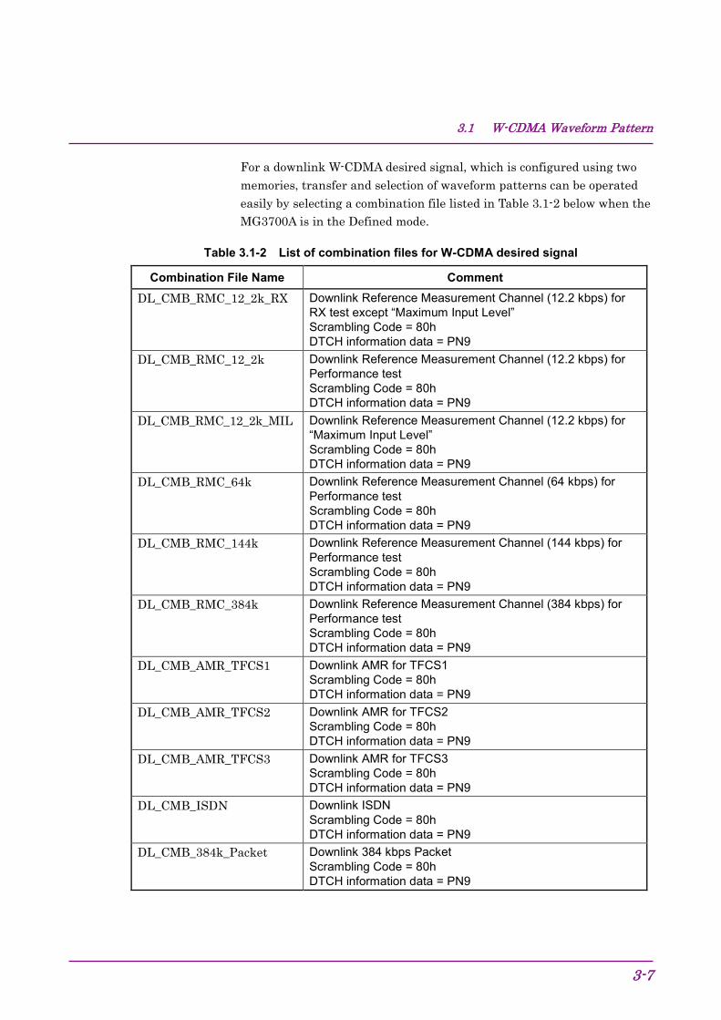
For a downlink W-CDMA desired signal, which is configured using two memories, transfer and selection of waveform patterns can be operated easily by selecting a combination file listed in Table 3.1-2 below when the MG3700A is in the Defined mode.
Table 3.1-2 List of combination files for W-CDMA desired signal
Combination File Name Comment DL_CMB_RMC_12_2k_RX Downlink Reference Measurement Channel (12.2 kbps) for
RX test except “Maximum Input Level” Scrambling Code = 80h DTCH information data = PN9
DL_CMB_RMC_12_2k Downlink Reference Measurement Channel (12.2 kbps) for Performance test Scrambling Code = 80h DTCH information data = PN9
DL_CMB_RMC_12_2k_MIL Downlink Reference Measurement Channel (12.2 kbps) for “Maximum Input Level” Scrambling Code = 80h DTCH information data = PN9
DL_CMB_RMC_64k Downlink Reference Measurement Channel (64 kbps) for Performance test Scrambling Code = 80h DTCH information data = PN9
DL_CMB_RMC_144k Downlink Reference Measurement Channel (144 kbps) for Performance test Scrambling Code = 80h DTCH information data = PN9
DL_CMB_RMC_384k Downlink Reference Measurement Channel (384 kbps) for Performance test Scrambling Code = 80h DTCH information data = PN9
DL_CMB_AMR_TFCS1 Downlink AMR for TFCS1 Scrambling Code = 80h DTCH information data = PN9
DL_CMB_AMR_TFCS2 Downlink AMR for TFCS2 Scrambling Code = 80h DTCH information data = PN9
DL_CMB_AMR_TFCS3 Downlink AMR for TFCS3 Scrambling Code = 80h DTCH information data = PN9
DL_CMB_ISDN Downlink ISDN Scrambling Code = 80h DTCH information data = PN9
DL_CMB_384k_Packet Downlink 384 kbps Packet Scrambling Code = 80h DTCH information data = PN9
Section 3 Details of Standard Waveform Pattern
3-8
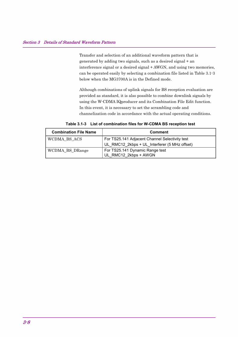
Transfer and selection of an additional waveform pattern that is generated by adding two signals, such as a desired signal + an interference signal or a desired signal + AWGN, and using two memories, can be operated easily by selecting a combination file listed in Table 3.1-3 below when the MG3700A is in the Defined mode.
Although combinations of uplink signals for BS reception evaluation are provided as standard, it is also possible to combine downlink signals by using the W-CDMA IQproducer and its Combination File Edit function. In this event, it is necessary to set the scrambling code and channelization code in accordance with the actual operating conditions.
Table 3.1-3 List of combination files for W-CDMA BS reception test
Combination File Name Comment
WCDMA_BS_ACS For TS25.141 Adjacent Channel Selectivity test UL_RMC12_2kbps + UL_Interferer (5 MHz offset)
WCDMA_BS_DRange For TS25.141 Dynamic Range test UL_RMC12_2kbps + AWGN
3.1 W-CDMA Waveform Pattern
3-9
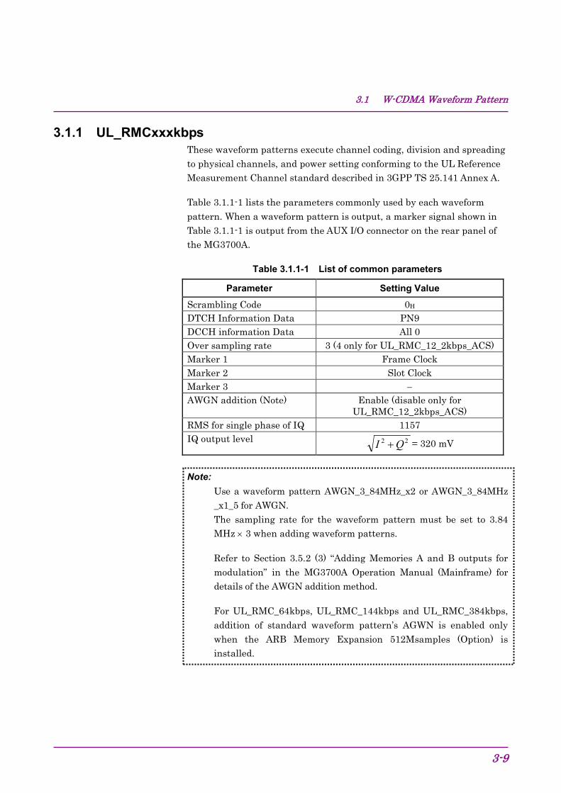
3.1.1 UL_RMCxxxkbps These waveform patterns execute channel coding, division and spreading to physical channels, and power setting conforming to the UL Reference Measurement Channel standard described in 3GPP TS 25.141 Annex A.
Table 3.1.1-1 lists the parameters commonly used by each waveform pattern. When a waveform pattern is output, a marker signal shown in Table 3.1.1-1 is output from the AUX I/O connector on the rear panel of the MG3700A.
Table 3.1.1-1 List of common parameters
Parameter Setting Value
Scrambling Code 0H DTCH Information Data PN9 DCCH information Data All 0 Over sampling rate 3 (4 only for UL_RMC_12_2kbps_ACS) Marker 1 Frame Clock Marker 2 Slot Clock Marker 3 − AWGN addition (Note) Enable (disable only for
UL_RMC_12_2kbps_ACS) RMS for single phase of IQ 1157 IQ output level 22 QI + = 320 mV
Note:
Use a waveform pattern AWGN_3_84MHz_x2 or AWGN_3_84MHz _x1_5 for AWGN. The sampling rate for the waveform pattern must be set to 3.84 MHz × 3 when adding waveform patterns.
Refer to Section 3.5.2 (3) “Adding Memories A and B outputs for modulation” in the MG3700A Operation Manual (Mainframe) for details of the AWGN addition method.
For UL_RMC_64kbps, UL_RMC_144kbps and UL_RMC_384kbps, addition of standard waveform pattern’s AGWN is enabled only when the ARB Memory Expansion 512Msamples (Option) is installed.
Section 3 Details of Standard Waveform Pattern
3-10
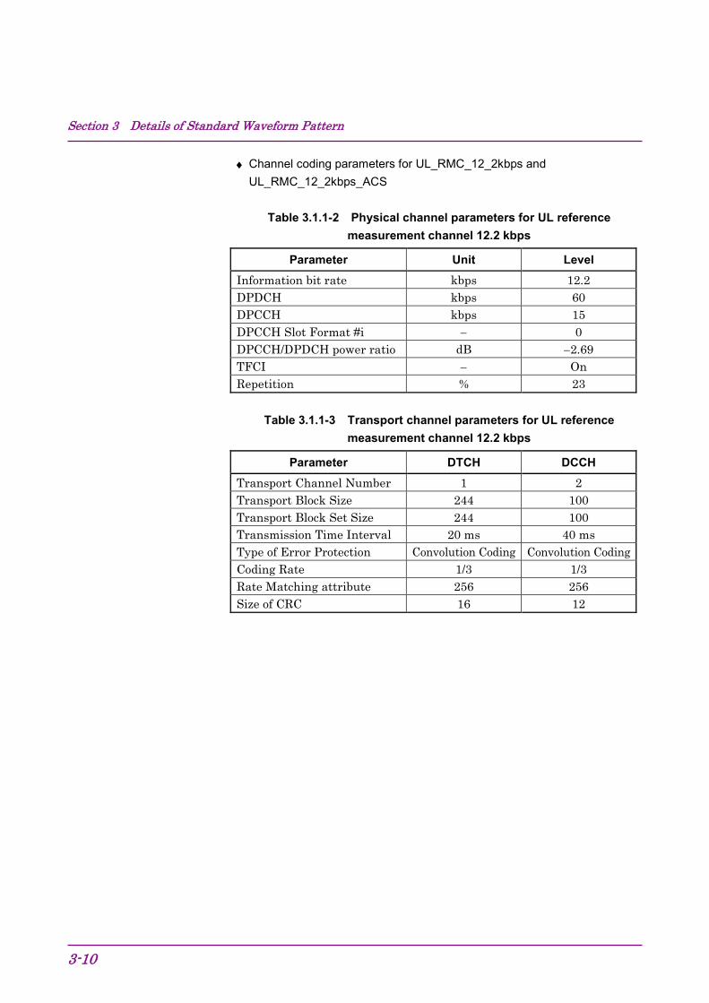
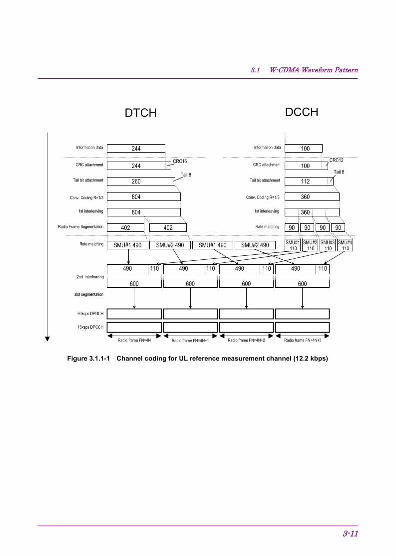
♦ Channel coding parameters for UL_RMC_12_2kbps and UL_RMC_12_2kbps_ACS
Table 3.1.1-2 Physical channel parameters for UL reference measurement channel 12.2 kbps
Parameter Unit Level Information bit rate kbps 12.2 DPDCH kbps 60 DPCCH kbps 15 DPCCH Slot Format #i − 0 DPCCH/DPDCH power ratio dB −2.69 TFCI − On Repetition % 23
Table 3.1.1-3 Transport channel parameters for UL reference measurement channel 12.2 kbps
Parameter DTCH DCCH Transport Channel Number 1 2 Transport Block Size 244 100 Transport Block Set Size 244 100 Transmission Time Interval 20 ms 40 ms Type of Error Protection Convolution Coding Convolution Coding Coding Rate 1/3 1/3 Rate Matching attribute 256 256 Size of CRC 16 12
3.1 W-CDMA Waveform Pattern
3-11
DCCHDTCH
15ksps DPCCH
Conv. Coding R=1/3
Radio frame FN=4N+1 Radio frame FN=4N+2 Radio frame FN=4N+3Radio frame FN=4N
Information data
CRC attachment
Radio Frame Segmentation
2nd interleaving600
490 110
804
804
260Tail 8
CRC16244
244
112Tail 8
100
CRC12
1st interleaving
Rate matching
slot segmentation
CRC attachment
Tail bit attachment
Conv. Coding R=1/3
SMU#1 490
Tail bit attachment
402 90Rate matching
1st interleaving
Information data
100
402
SMU#2 490 SMU#1 490 SMU#2 490
490 110 490 110 490 110
600 600 600
60ksps DPDCH
SMU#1 110
SMU#2 110
SMU#3 110
SMU#4 110
90 90 90
360
360
Figure 3.1.1-1 Channel coding for UL reference measurement channel (12.2 kbps)
Section 3 Details of Standard Waveform Pattern
3-12
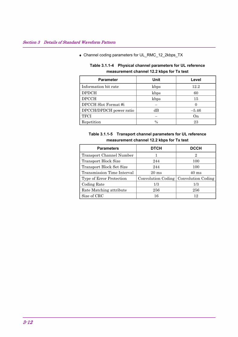
♦ Channel coding parameters for UL_RMC_12_2kbps_TX
Table 3.1.1-4 Physical channel parameters for UL reference measurement channel 12.2 kbps for Tx test
Parameter Unit Level Information bit rate kbps 12.2 DPDCH kbps 60 DPCCH kbps 15 DPCCH Slot Format #i − 0 DPCCH/DPDCH power ratio dB –5.46 TFCI − On Repetition % 23
Table 3.1.1-5 Transport channel parameters for UL reference
measurement channel 12.2 kbps for Tx test
Parameters DTCH DCCH Transport Channel Number 1 2 Transport Block Size 244 100 Transport Block Set Size 244 100 Transmission Time Interval 20 ms 40 ms Type of Error Protection Convolution Coding Convolution Coding Coding Rate 1/3 1/3 Rate Matching attribute 256 256 Size of CRC 16 12

3.1 W-CDMA Waveform Pattern
3-13
DCCHDTCH
15ksps DPCCH
Conv. Coding R=1/3
Radio frame FN=4N+1 Radio frame FN=4N+2 Radio frame FN=4N+3Radio frame FN=4N
Information data
CRC attachment
Radio Frame Segmentation
2nd interleaving600
490 110
804
804
260Tail 8
CRC16244
244
112Tail 8
100
CRC12
1st interleaving
Rate matching
slot segmentation
CRC attachment
Tail bit attachment
Conv. CodingR=1/3
SMU#1 490
Tail bit attachment
402 90Rate matching
1st interleaving
Information data
100
402
SMU#2 490 SMU#1 490 SMU#2 490
490 110 490 110 490 110
600 600 600
60ksps DPDCH
SMU#1 110
SMU#2 110
SMU#3 110
SMU#4 110
90 90 90
360
360
Figure 3.1.1-2 Channel coding for UL reference measurement channel (12.2 kbps)
Section 3 Details of Standard Waveform Pattern
3-14
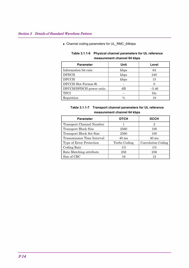
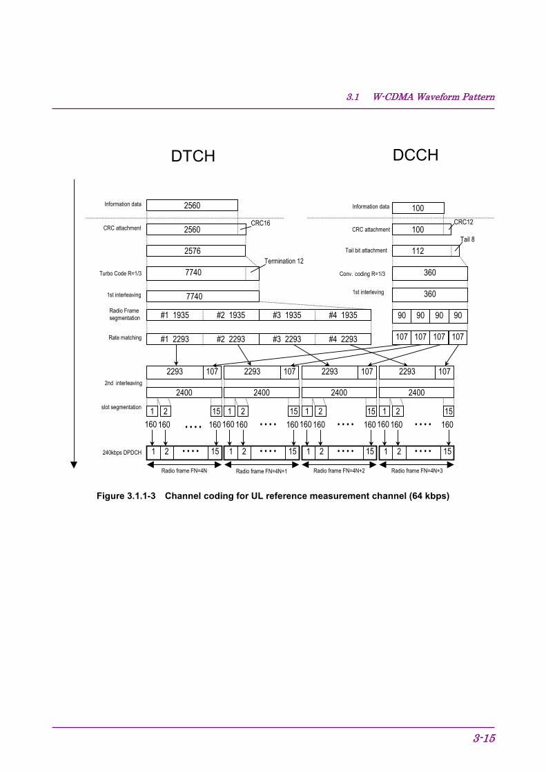
♦ Channel coding parameters for UL_RMC_64kbps
Table 3.1.1-6 Physical channel parameters for UL reference measurement channel 64 kbps
Parameter Unit Level Information bit rate kbps 64 DPDCH kbps 240 DPCCH kbps 15 DPCCH Slot Format #i − 0 DPCCH/DPDCH power ratio dB −5.46 TFCI − On Repetition % 18
Table 3.1.1-7 Transport channel parameters for UL reference measurement channel 64 kbps
Parameter DTCH DCCH Transport Channel Number 1 2 Transport Block Size 2560 100 Transport Block Set Size 2560 100 Transmission Time Interval 40 ms 40 ms Type of Error Protection Turbo Coding Convolution Coding Coding Rate 1/3 1/3 Rate Matching attribute 256 256 Size of CRC 16 12
3.1 W-CDMA Waveform Pattern
3-15
2293
DCCHDTCH
240kbps DPDCH
Turbo Code R=1/3
1 2 15
Radio frame FN=4N+1 Radio frame FN=4N+2 Radio frame FN=4N+3Radio frame FN=4N
Information data
CRC attachment
Rate matching
2nd interleaving2400
1601
• • • •
2293 107
2400 2400 2400
7740
7740
2576Termination 12
CRC162560
2560
112Tail 8
100CRC12
1st interleaving
Radio Framesegmentation
slot segmentation
CRC attachment
Tail bit attachment
Conv. coding R=1/3
1st interleving
#1 1935 90
• • • • • • • • • • • •
• • • •
#2 1935 #3 1935 #4 1935
#1 2293 #2 2293 #3 2293 #4 2293
2293 107 107 2293 107
107 107 107 107
90 90 90
360
360
2 15160 160 160
1 2 15160 160
1 2 15• • • •
1601 2 15
160 160
1 2 15• • • •
1601 2 15
160 160
1 2 15• • • •
100Information data
Figure 3.1.1-3 Channel coding for UL reference measurement channel (64 kbps)

Section 3 Details of Standard Waveform Pattern
3-16
♦ Channel coding parameters for UL_RMC_144kbps
Table 3.1.1-8 Physical channel parameters for UL reference measurement channel 144 kbps
Parameter Unit Level Information bit rate kbps 144 DPDCH kbps 480 DPCCH kbps 15 DPCCH Slot Format #i − 0 DPCCH/DPDCH power ratio dB −9.54 TFCI − On Repetition % 8
Table 3.1.1-9 Transport channel parameters for UL reference measurement channel 144 kbps
Parameter DTCH DCCH Transport Channel Number 1 2 Transport Block Size 2880 100 Transport Block Set Size 5760 100 Transmission Time Interval 40 ms 40 ms Type of Error Protection Turbo Coding Convolution Coding Coding Rate 1/3 1/3 Rate Matching attribute 256 256 Size of CRC 16 12
3.1 W-CDMA Waveform Pattern
3-17
4702
DCCHDTCH
480kbps DPDCH
Turbo Code R=1/3
1 2 15
Radio frame FN=4N+1 Radio frame FN=4N+2 Radio frame FN=4N+3Radio frame FN=4N
Information data
CRC attachment
Rate matching
2nd interleaving4800
3201
• • • •
4702 98
4800 4800 4800
17400
5792Termination 2x12
CRC16
2880
2880
112Tail 8
100CRC12
1st interleaving
Radio Framesegmentation
slot segmentation
CRC attachment
Tail bit attachment
Conv. coding R=1/3
1st interleving
#1 4350
• • • • • • • • • • • •
• • • •
#2 4350 #3 4350 #4 4350
#1 4702 #2 4702 #3 4702 #4 4702
4702 98 98 4702 98
#1 98
360
360
2 15320 320 320
1 2 15320 320
1 2 15• • • •
3201 2 15
320 320
1 2 15• • • •
3201 2 15
320 320
1 2 15• • • •
2880
2880CRC16
17400
#2 98 #3 98 #4 98
#1 90 #2 90 #3 90 #4 90
Information data 100
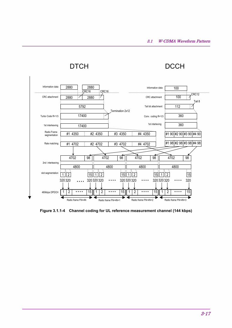
Figure 3.1.1-4 Channel coding for UL reference measurement channel (144 kbps)
Section 3 Details of Standard Waveform Pattern
3-18
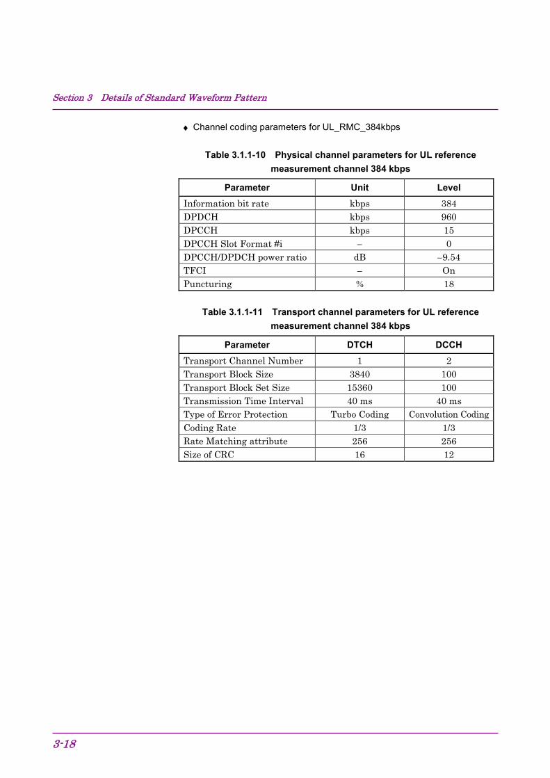
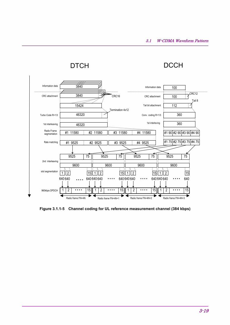
♦ Channel coding parameters for UL_RMC_384kbps
Table 3.1.1-10 Physical channel parameters for UL reference measurement channel 384 kbps
Parameter Unit Level Information bit rate kbps 384 DPDCH kbps 960 DPCCH kbps 15 DPCCH Slot Format #i − 0 DPCCH/DPDCH power ratio dB −9.54 TFCI − On Puncturing % 18
Table 3.1.1-11 Transport channel parameters for UL reference measurement channel 384 kbps
Parameter DTCH DCCH Transport Channel Number 1 2 Transport Block Size 3840 100 Transport Block Set Size 15360 100 Transmission Time Interval 40 ms 40 ms Type of Error Protection Turbo Coding Convolution Coding Coding Rate 1/3 1/3 Rate Matching attribute 256 256 Size of CRC 16 12
3.1 W-CDMA Waveform Pattern
3-19
9525
DCCHDTCH
960kbps DPDCH
Turbo Code R=1/3
1 2 15
Radio frame FN=4N+1 Radio frame FN=4N+2 Radio frame FN=4N+3Radio frame FN=4N
Information data
CRC attachment
Rate matching
2nd interleaving9600
6401
• • • •
9525 75
9600 9600 9600
46320
46320
15424Termination 4x12
CRC16
2560
112Tail 8
100CRC12
1st interleaving
Radio Framesegmentation
slot segmentation
CRC attachment
Tail bit attachment
Conv. coding R=1/3
1st interleving
#1 11580
• • • • • • • • • • • •
• • • •
#2 11580 #3 11580 #4 11580
#1 9525 #2 9525 #3 9525 #4 9525
9525 75 75 9525 75
#1 75
#1 90
360
360
2 15640 640 640
1 2 15640 640
1 2 15• • • •
6401 2 15
640 640
1 2 15• • • •
6401 2 15
640 640
1 2 15• • • •
256025603840
3840
#2 75
#2 90
#3 75
#3 90
#4 75
#4 90
100Information data
Figure 3.1.1-5 Channel coding for UL reference measurement channel (384 kbps)
Section 3 Details of Standard Waveform Pattern
3-20
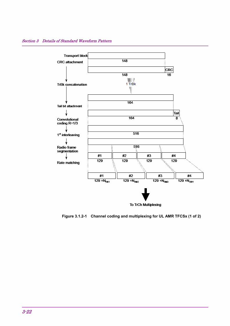
3.1.2 UL_AMR_TFCSx/UL_ISDN/UL_64kbps_Packet These waveform patterns execute channel coding, division and spreading to physical channels, and power setting conforming to the Channel coding and multiplexing example (Uplink) standard described in 3GPP TS 25.944 Section 4.1.2.
Table 3.1.2-1 lists the parameters commonly used by each waveform pattern When a waveform pattern is output, a marker signal shown in Table 3.1.2-1 is output from the AUX I/O connector on the rear panel of the MG3700A.
Table 3.1.2-1 List of common parameters
Parameter Setting Value
Scrambling Code 0H DTCH Information Data PN9 DCCH Information Data All 0 Over sampling rate 3 Marker 1 Frame Clock Marker 2 Slot Clock Marker 3 − AWGN addition (Note) Enable RMS for single phase of IQ 1157 IQ output level 22 QI + = 320 mV
Note:
Use a waveform pattern AWGN_3_84MHz_x2 or AWGN_3_84MHz _x1_5 for AWGN. The sampling rate for the waveform pattern must be set to 3.84 MHz × 3 when adding waveform patterns.
Refer to Section 3.5.2 (3) “Adding Memories A and B outputs for modulation” in the MG3700A Operation Manual (Mainframe) for details of the AWGN addition method.
For UL_ISDN, addition of standard waveform pattern’s AGWN is enabled only when the ARB Memory Expansion 512Msamples (Option) is installed.
3.1 W-CDMA Waveform Pattern
3-21
♦ Channel coding parameters for UL_AMR_TFCSx
Table 3.1.2-2 Physical channel parameters for UL_AMR_TFCSx
Parameter Unit Level DPDCH kbps 60 DPCCH kbps 15 DPCCH Slot Format #i − 0 DPCCH/DPDCH power ratio dB −2.69
Table 3.1.2-3 Parameters for 3.4 kbps data (DCCH)
Transport Block Size 148 bits Transport Block Set Size 148 bits Rate Matching attribute 160 CRC 16 bits Coding CC, coding rate = 1/3 TTI 40 ms
Section 3 Details of Standard Waveform Pattern
3-22
Figure 3.1.2-1 Channel coding and multiplexing for UL AMR TFCSx (1 of 2)
3.1 W-CDMA Waveform Pattern
3-23
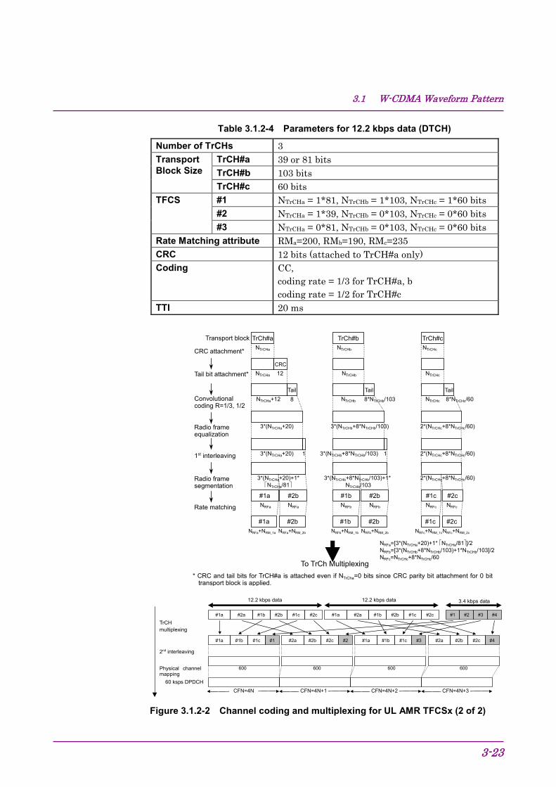
Table 3.1.2-4 Parameters for 12.2 kbps data (DTCH)
Number of TrCHs 3 Transport Block Size
TrCH#a 39 or 81 bits TrCH#b 103 bits TrCH#c 60 bits
TFCS #1 NTrCHa = 1*81, NTrCHb = 1*103, NTrCHc = 1*60 bits #2 NTrCHa = 1*39, NTrCHb = 0*103, NTrCHc = 0*60 bits #3 NTrCHa = 0*81, NTrCHb = 0*103, NTrCHc = 0*60 bits
Rate Matching attribute RMa=200, RMb=190, RMc=235 CRC 12 bits (attached to TrCH#a only) Coding CC,
coding rate = 1/3 for TrCH#a, b coding rate = 1/2 for TrCH#c
TTI 20 ms
TrCh#aTransport block
CRC attachment*
CRC
Tail bit attachment*
Convolutionalcoding R=1/3, 1/2
Rate matching
NTrCHa
NTrCHa
3*(NTrCHa+20)
Tail8NTrCHa+12
1st interleaving
12
Radio framesegmentation
#1a
To TrCh Multiplexing
TrCh#bNTrCHb
NTrCHb
3*(NTrCHb+8*NTrCHb/103)
Tail8*NTrCHb/103NTrCHb
TrCh#cNTrCHc
NTrCHc
2*(NTrCHc+8*NTrCHc/60)
Tail8*NTrCHc/60NTrCHc
#1c #2c
Radio frameequalization
3*(NTrCHa+20) 3*(NTrCHb+8*NTrCHb/103) 2*(NTrCHc+8*NTrCHc/60)1 1
#2b #1b #2b
3*(NTrCHa+20)+1*NTrCHa/81
3*(NTrCHb+8*NTrCHb/103)+1*NTrCHb/103
2*(NTrCHc+8*NTrCHc/60)
#1a
NRFa NRFa NRFb NRFb NRFc NRFc
#2b #1b #2b #1c #2cNRFa+NRM_1a NRFa+NRM_2b NRFb+NRM_1b NRFb+NRM_2b NRFc+NRM_1cNRFc+NRM_2c
NRFa=[3*(NTrCHa+20)+1* NTrCHa/81]/2NRFb=[3*(NTrCHb+8*NTrCHb/103)+1*NTrCHb/103]/2NRFc=NTrCHc+8*NTrCHc/60
* CRC and tail bits for TrCH#a is attached even if NTrCha=0 bits since CRC parity bit attachment for 0 bittransport block is applied.
12.2 kbps data 3.4 kbps data
TrCHmultiplexing
60 ksps DPDCH
2nd interleaving
Physical channelmapping
#1#1a #1c
CFN=4N CFN=4N+1
#1b #2#2a #2c#2b #3#1a #1c#1b #4#2a #2c#2b
#1a #2a #1b #2b #1c #2c #1a #2a #1b #2b #1c #2c #1 #2 #3 #4
600 600 600 600
12.2 kbps data
CFN=4N+2 CFN=4N+3
Figure 3.1.2-2 Channel coding and multiplexing for UL AMR TFCSx (2 of 2)
Section 3 Details of Standard Waveform Pattern
3-24
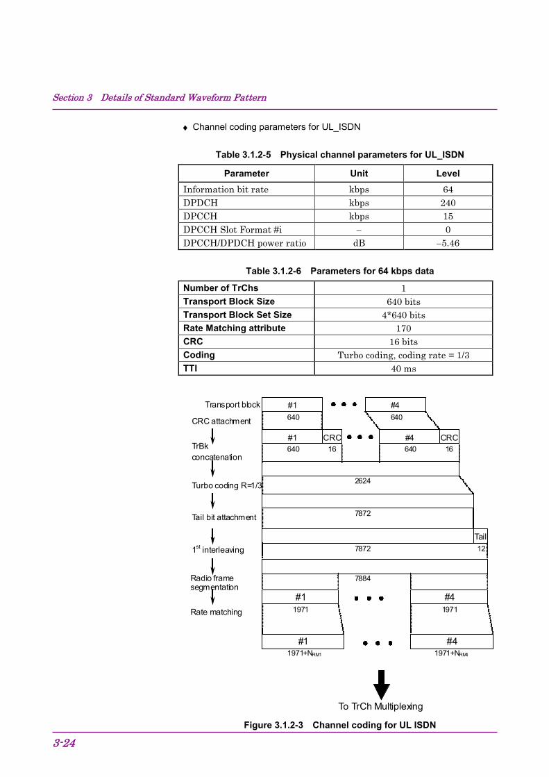
♦ Channel coding parameters for UL_ISDN
Table 3.1.2-5 Physical channel parameters for UL_ISDN
Parameter Unit Level Information bit rate kbps 64 DPDCH kbps 240 DPCCH kbps 15 DPCCH Slot Format #i − 0 DPCCH/DPDCH power ratio dB −5.46
Table 3.1.2-6 Parameters for 64 kbps data
Number of TrChs 1 Transport Block Size 640 bits Transport Block Set Size 4*640 bits Rate Matching attribute 170 CRC 16 bits Coding Turbo coding, coding rate = 1/3 TTI 40 ms
Turbo coding R=1/3
Rate matching
640 16
2624
640 16
7884
1st interleaving
Tail bit attachment
Tail 12
Radio frame segmentation
#1
1971+NRM1
#4
To TrCh Multiplexing
#1 #4
1971 1971
#1 Transport block
CRC attachment
#1 CRC
640 #4
#4 CRC
640
TrBk concatenation
1971+NRM4
7872
7872
Figure 3.1.2-3 Channel coding for UL ISDN
3.1 W-CDMA Waveform Pattern
3-25
#1
3.4 kbps data
#2 #3 #4
DPDCH
#1 #1 #2 #2 #1 #3 #2 #42nd interleaving
Physical channelmapping
#1 #2 #1 #2
64 kbps Packet data
CFN=4N
TrCHmultiplexing
64 kbps Packet data
CFN=4N+1 CFN=4N+2 CFN=4N+3
Figure 3.1.2-4 Multiplexing for UL ISDN
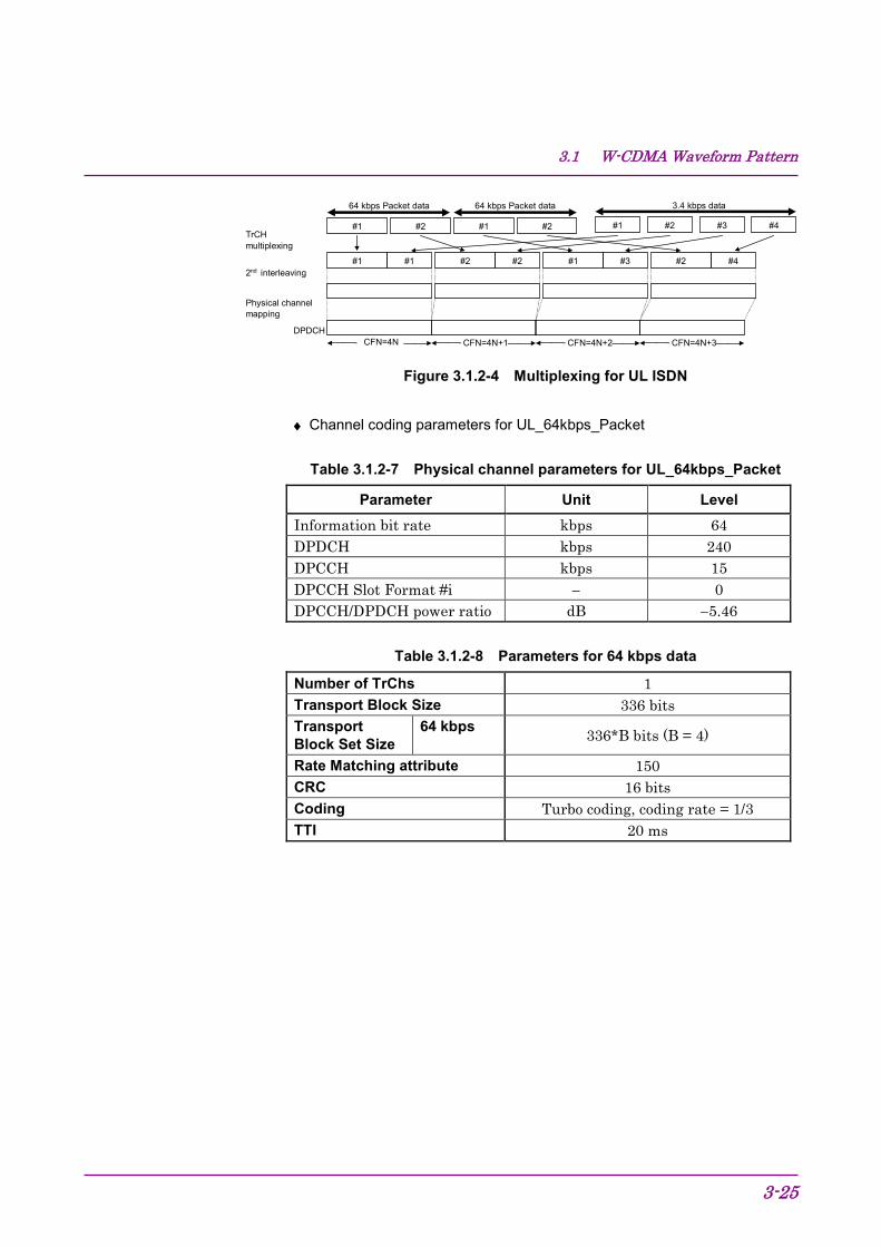
♦ Channel coding parameters for UL_64kbps_Packet
Table 3.1.2-7 Physical channel parameters for UL_64kbps_Packet
Parameter Unit Level Information bit rate kbps 64 DPDCH kbps 240 DPCCH kbps 15 DPCCH Slot Format #i − 0 DPCCH/DPDCH power ratio dB −5.46
Table 3.1.2-8 Parameters for 64 kbps data
Number of TrChs 1 Transport Block Size 336 bits Transport Block Set Size
64 kbps 336*B bits (B = 4)
Rate Matching attribute 150 CRC 16 bits Coding Turbo coding, coding rate = 1/3 TTI 20 ms
Section 3 Details of Standard Waveform Pattern
3-26
Transport block
CRC attachment
CRC
Turbo coding
Rate matching
336
336 16
352* B
1056* B +12*B/9
1st interleaving
1056* B Tail bit attachment
Tail 12*B/9 1056* B
#1
To TrCh Multiplexing
TrBk concatenation B TrBks (B= 4)
#2
Radio frame segmentation
(1056* B +12*B/9)/2 (1056* B +12*B/9)/2
#1 #2 (1056* B +12*B/9)/2+NRM1 (1056* B +12*B/9)/2+NRM2
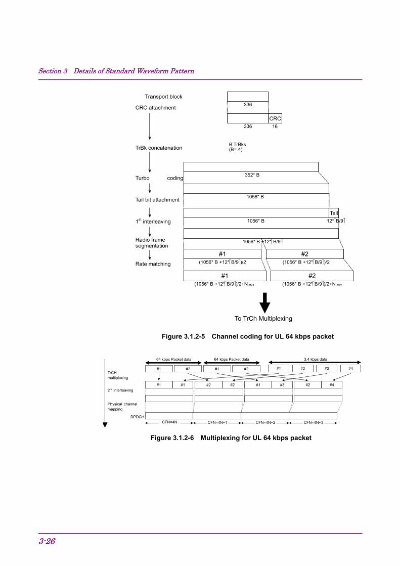
Figure 3.1.2-5 Channel coding for UL 64 kbps packet
#1
3.4 kbps data
#2 #3 #4
DPDCH
#1 #1 #2 #2 #1 #3 #2 #42nd interleaving
Physical channelmapping
#1 #2 #1 #2
64 kbps Packet data
CFN=4N
TrCHmultiplexing
64 kbps Packet data
CFN=4N+1 CFN=4N+2 CFN=4N+3
Figure 3.1.2-6 Multiplexing for UL 64 kbps packet
3.1 W-CDMA Waveform Pattern
3-27
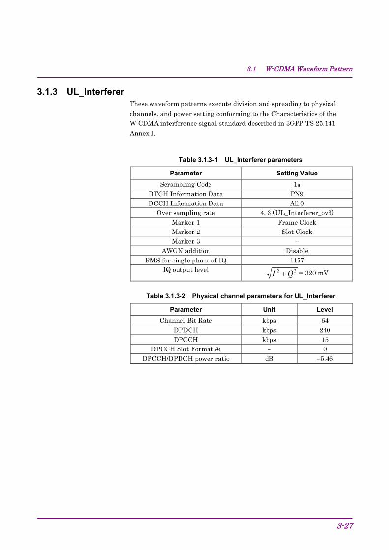
3.1.3 UL_Interferer These waveform patterns execute division and spreading to physical channels, and power setting conforming to the Characteristics of the W-CDMA interference signal standard described in 3GPP TS 25.141 Annex I.
Table 3.1.3-1 UL_Interferer parameters
Parameter Setting Value Scrambling Code 1H
DTCH Information Data PN9 DCCH Information Data All 0
Over sampling rate 4, 3 (UL_Interferer_ov3) Marker 1 Frame Clock Marker 2 Slot Clock Marker 3 −
AWGN addition Disable RMS for single phase of IQ 1157
IQ output level 22 QI + = 320 mV
Table 3.1.3-2 Physical channel parameters for UL_Interferer
Parameter Unit Level Channel Bit Rate kbps 64
DPDCH kbps 240 DPCCH kbps 15
DPCCH Slot Format #i − 0 DPCCH/DPDCH power ratio dB −5.46
Section 3 Details of Standard Waveform Pattern
3-28
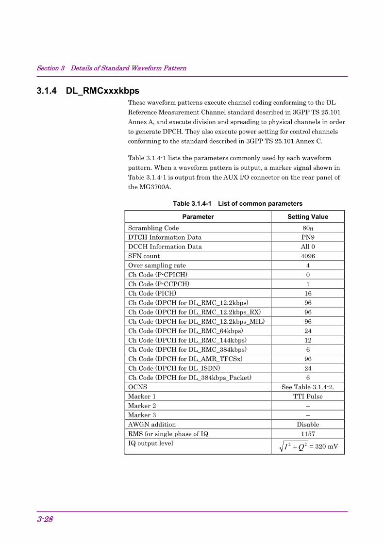
3.1.4 DL_RMCxxxkbps These waveform patterns execute channel coding conforming to the DL Reference Measurement Channel standard described in 3GPP TS 25.101 Annex A, and execute division and spreading to physical channels in order to generate DPCH. They also execute power setting for control channels conforming to the standard described in 3GPP TS 25.101 Annex C.
Table 3.1.4-1 lists the parameters commonly used by each waveform pattern. When a waveform pattern is output, a marker signal shown in Table 3.1.4-1 is output from the AUX I/O connector on the rear panel of the MG3700A.
Table 3.1.4-1 List of common parameters
Parameter Setting Value
Scrambling Code 80H DTCH Information Data PN9 DCCH Information Data All 0 SFN count 4096 Over sampling rate 4 Ch Code (P-CPICH) 0 Ch Code (P-CCPCH) 1 Ch Code (PICH) 16 Ch Code (DPCH for DL_RMC_12.2kbps) 96 Ch Code (DPCH for DL_RMC_12.2kbps_RX) 96 Ch Code (DPCH for DL_RMC_12.2kbps_MIL) 96 Ch Code (DPCH for DL_RMC_64kbps) 24 Ch Code (DPCH for DL_RMC_144kbps) 12 Ch Code (DPCH for DL_RMC_384kbps) 6 Ch Code (DPCH for DL_AMR_TFCSx) 96 Ch Code (DPCH for DL_ISDN) 24 Ch Code (DPCH for DL_384kbps_Packet) 6 OCNS See Table 3.1.4-2. Marker 1 TTI Pulse Marker 2 – Marker 3 – AWGN addition Disable RMS for single phase of IQ 1157 IQ output level 22 QI + = 320 mV
3.1 W-CDMA Waveform Pattern
3-29
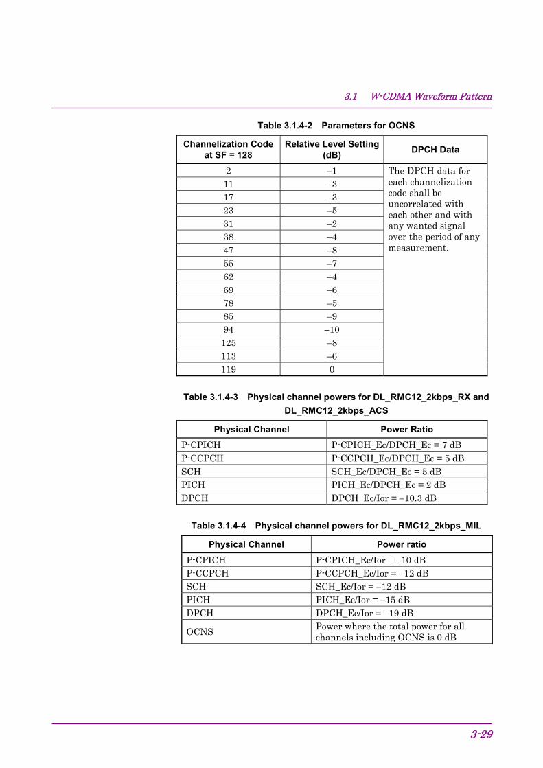
Table 3.1.4-2 Parameters for OCNS
Channelization Code at SF = 128
Relative Level Setting (dB) DPCH Data
2 −1 The DPCH data for each channelization code shall be uncorrelated with each other and with any wanted signal over the period of any measurement.
11 −3 17 −3 23 −5 31 −2 38 −4 47 −8 55 −7 62 −4 69 −6 78 −5 85 −9 94 −10 125 −8 113 −6 119 0
Table 3.1.4-3 Physical channel powers for DL_RMC12_2kbps_RX and
DL_RMC12_2kbps_ACS
Physical Channel Power Ratio P-CPICH P-CPICH_Ec/DPCH_Ec = 7 dB P-CCPCH P-CCPCH_Ec/DPCH_Ec = 5 dB SCH SCH_Ec/DPCH_Ec = 5 dB PICH PICH_Ec/DPCH_Ec = 2 dB DPCH DPCH_Ec/Ior = −10.3 dB
Table 3.1.4-4 Physical channel powers for DL_RMC12_2kbps_MIL
Physical Channel Power ratio P-CPICH P-CPICH_Ec/Ior = −10 dB P-CCPCH P-CCPCH_Ec/Ior = −12 dB SCH SCH_Ec/Ior = −12 dB PICH PICH_Ec/Ior = −15 dB DPCH DPCH_Ec/Ior = –19 dB
OCNS Power where the total power for all channels including OCNS is 0 dB
Section 3 Details of Standard Waveform Pattern
3-30
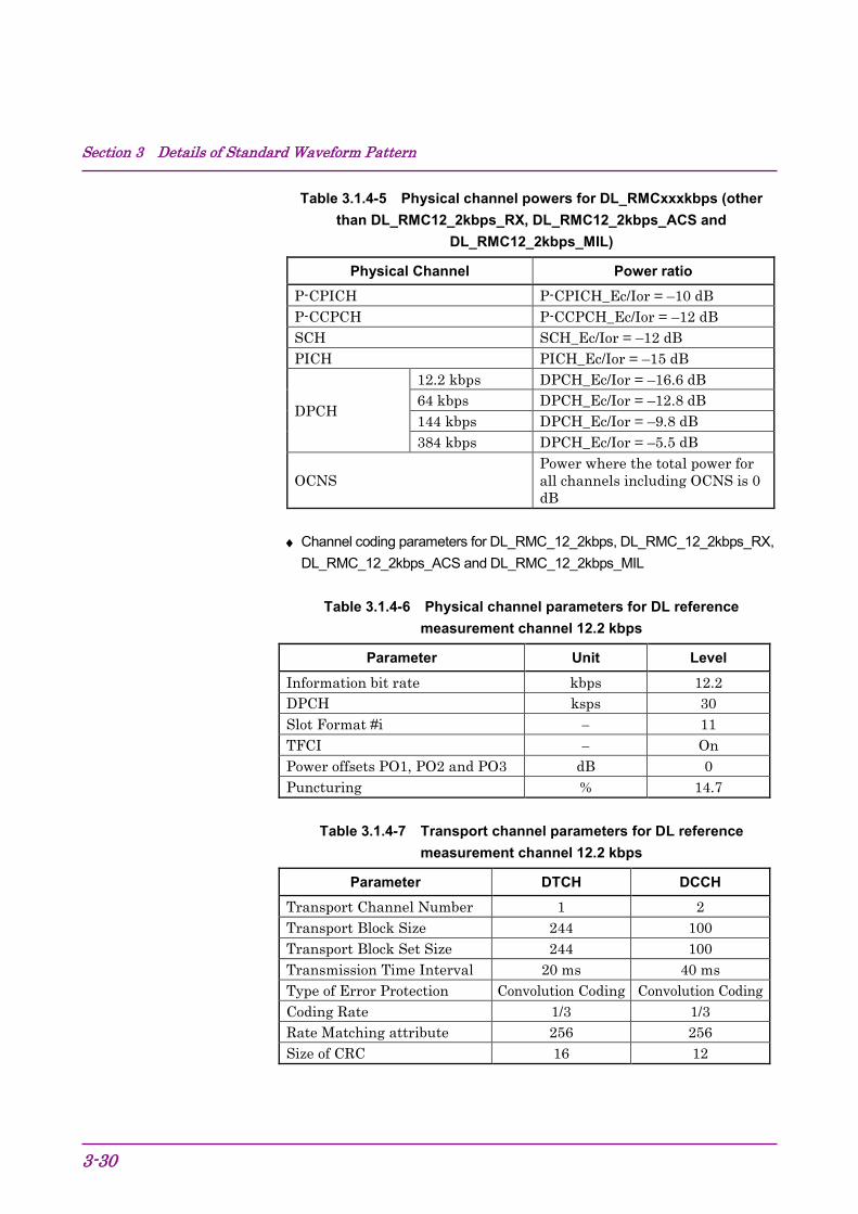
Table 3.1.4-5 Physical channel powers for DL_RMCxxxkbps (other than DL_RMC12_2kbps_RX, DL_RMC12_2kbps_ACS and
DL_RMC12_2kbps_MIL)
Physical Channel Power ratio P-CPICH P-CPICH_Ec/Ior = –10 dB P-CCPCH P-CCPCH_Ec/Ior = –12 dB SCH SCH_Ec/Ior = –12 dB PICH PICH_Ec/Ior = –15 dB
DPCH
12.2 kbps DPCH_Ec/Ior = –16.6 dB 64 kbps DPCH_Ec/Ior = –12.8 dB 144 kbps DPCH_Ec/Ior = –9.8 dB 384 kbps DPCH_Ec/Ior = –5.5 dB
OCNS Power where the total power for all channels including OCNS is 0 dB
♦ Channel coding parameters for DL_RMC_12_2kbps, DL_RMC_12_2kbps_RX,
DL_RMC_12_2kbps_ACS and DL_RMC_12_2kbps_MIL
Table 3.1.4-6 Physical channel parameters for DL reference measurement channel 12.2 kbps
Parameter Unit Level
Information bit rate kbps 12.2 DPCH ksps 30 Slot Format #i − 11 TFCI − On Power offsets PO1, PO2 and PO3 dB 0 Puncturing % 14.7
Table 3.1.4-7 Transport channel parameters for DL reference measurement channel 12.2 kbps
Parameter DTCH DCCH Transport Channel Number 1 2 Transport Block Size 244 100 Transport Block Set Size 244 100 Transmission Time Interval 20 ms 40 ms Type of Error Protection Convolution Coding Convolution Coding Coding Rate 1/3 1/3 Rate Matching attribute 256 256 Size of CRC 16 12
3.1 W-CDMA Waveform Pattern
3-31
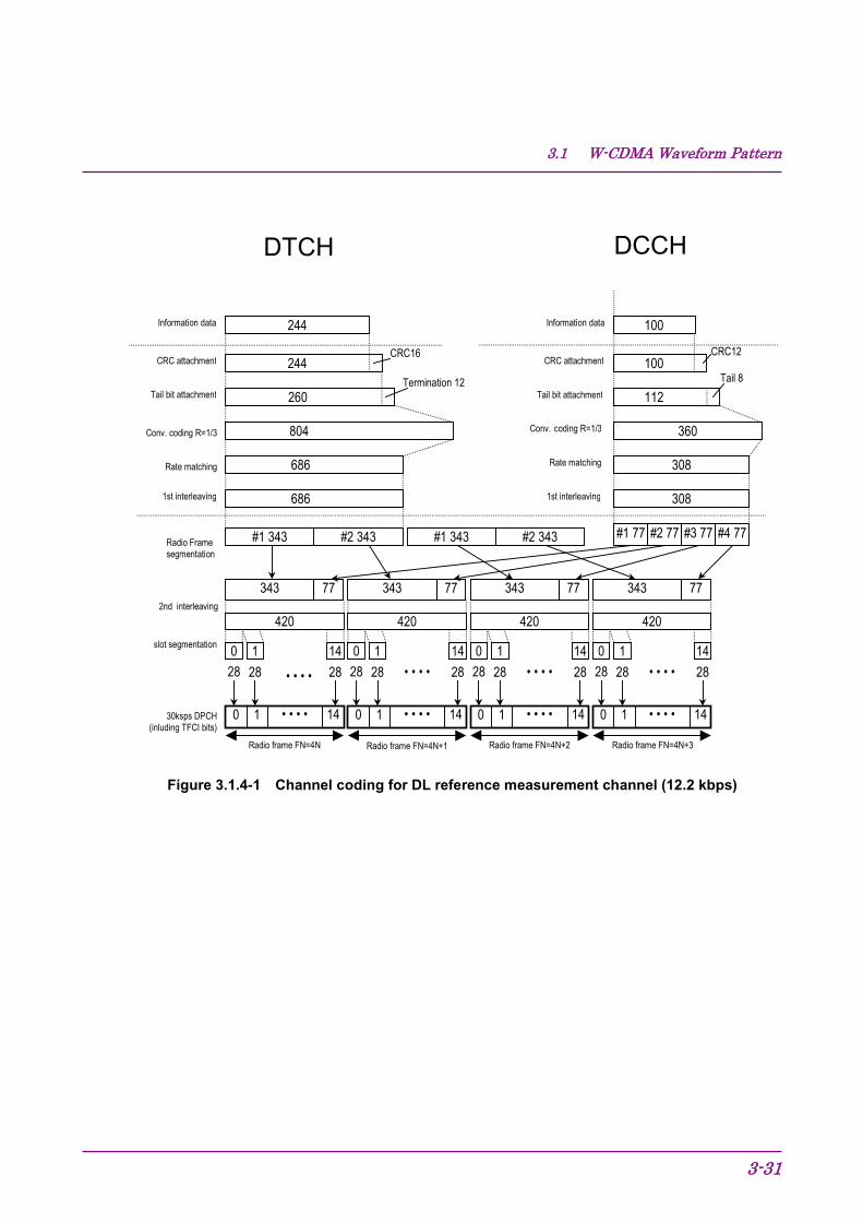
343
DCCHDTCH
30ksps DPCH(inluding TFCI bits)
Conv. coding R=1/3
0 1 14
Radio frame FN=4N+1 Radio frame FN=4N+2 Radio frame FN=4N+3Radio frame FN=4N
Information data
CRC attachment
Rate matching
2nd interleaving420
280
• • • •
343 77
420 420 420
686
804
260Termination 12
CRC16244
244
112Tail 8
100
CRC12
1st interleaving
Radio Framesegmentation
slot segmentation
CRC attachment
Tail bit attachment
Conv. coding R=1/3
• • • • • • • • • • • •
• • • •
#1 343 #2 343 #1 343 #2 343
343 77 77 343 77
#1 77
308
360
1 1428 28
0 1 14
• • • •
0 1 14
• • • •
0 1 14
• • • •
Tail bit attachment
686
28 28 28 28 28 28 28 28 28
0 1 14 0 1 14 0 1 14
#2 77 #3 77 #4 77
308
Rate matching
1st interleaving
Information data
100
Figure 3.1.4-1 Channel coding for DL reference measurement channel (12.2 kbps)

Section 3 Details of Standard Waveform Pattern
3-32
♦ Channel coding parameters for DL_RMC_64kbps
Table 3.1.4-8 Physical channel parameters for DL reference measurement channel 64 kbps
Parameter Unit Level Information bit rate kbps 64 DPCH ksps 120 Slot Format #i − 13 TFCI − On Power offsets PO1, PO2 and PO3 dB 0 Repetition % 2.9
Table 3.1.4-9 Transport channel parameters for DL reference measurement channel 64 kbps
Parameter DTCH DCCH Transport Channel Number 1 2 Transport Block Size 1280 100 Transport Block Set Size 1280 100 Transmission Time Interval 20 ms 40 ms Type of Error Protection Turbo Coding Convolution Coding Coding Rate 1/3 1/3 Rate Matching attribute 256 256 Size of CRC 16 12 Position of TrCH in radio frame fixed fixed
3.1 W-CDMA Waveform Pattern
3-33
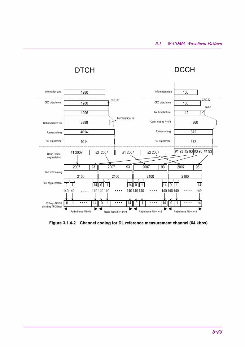
2007
DCCHDTCH
120ksps DPCH(inluding TFCI bits)
Turbo Code R=1/3
0 1 14
Radio frame FN=4N+1 Radio frame FN=4N+2 Radio frame FN=4N+3Radio frame FN=4N
Information data
CRC attachment
Rate matching
2nd interleaving2100
1400
• • • •
2007 93
2100 2100 2100
4014
3888
1296Termination 12
CRC161280
1280
112Tail 8
100
CRC12
1st interleaving
Radio Framesegmentation
slot segmentation
CRC attachment
Tail bit attachmet
Conv. coding R=1/3
• • • • • • • • • • • •
• • • •
#1 2007 #2 2007 #1 2007 #2 2007
2007 93 93 2007 93
#1 93
372
360
1 14 0 1 14
• • • •
0 1 14
• • • •
0 1 14
• • • •
4014
0 1 14 0 1 14 0 1 14
#2 93 #3 93 #4 93
372
Rate matching
1st interleaving
Information data
100
140 140 140 140 140 140 140 140 140 140 140
Figure 3.1.4-2 Channel coding for DL reference measurement channel (64 kbps)
Section 3 Details of Standard Waveform Pattern
3-34
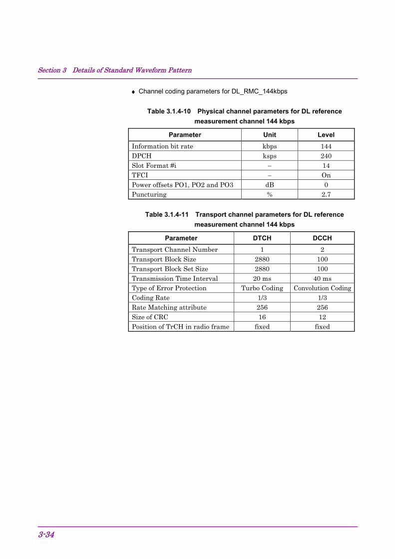
♦ Channel coding parameters for DL_RMC_144kbps
Table 3.1.4-10 Physical channel parameters for DL reference measurement channel 144 kbps
Parameter Unit Level Information bit rate kbps 144 DPCH ksps 240 Slot Format #i − 14 TFCI − On Power offsets PO1, PO2 and PO3 dB 0 Puncturing % 2.7
Table 3.1.4-11 Transport channel parameters for DL reference measurement channel 144 kbps
Parameter DTCH DCCH Transport Channel Number 1 2 Transport Block Size 2880 100 Transport Block Set Size 2880 100 Transmission Time Interval 20 ms 40 ms Type of Error Protection Turbo Coding Convolution Coding Coding Rate 1/3 1/3 Rate Matching attribute 256 256 Size of CRC 16 12 Position of TrCH in radio frame fixed fixed
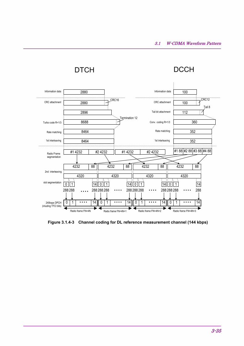
3.1 W-CDMA Waveform Pattern
3-35
4232
DCCHDTCH
240ksps DPCH(inluding TFCI bits)
Turbo code R=1/3
0 1 14
Radio frame FN=4N+1 Radio frame FN=4N+2 Radio frame FN=4N+3Radio frame FN=4N
Information data
CRC attachment
Rate matching
2nd interleaving4320
2880
• • • •
4232 88
4320 4320 4320
8464
8688
2896Termination 12
CRC162880
2880
112Tail 8
100
CRC12
1st interleaving
Radio Framesegmentation
slot segmentation
CRC attachment
Tail bit attachment
Conv. coding R=1/3
• • • • • • • • • • • •
• • • •
#1 4232 #2 4232 #1 4232 #2 4232
4232 88 88 4232 88
#1 88
352
360
1 14 0 1 14
• • • •
0 1 14
• • • •
0 1 14
• • • •
8464
0 1 14 0 1 14 0 1 14
#2 88 #3 88 #4 88
352
Rate matching
1st interleaving
Information data
100
288 288 288 288 288 288 288 288 288 288 288
Figure 3.1.4-3 Channel coding for DL reference measurement channel (144 kbps)
Section 3 Details of Standard Waveform Pattern
3-36
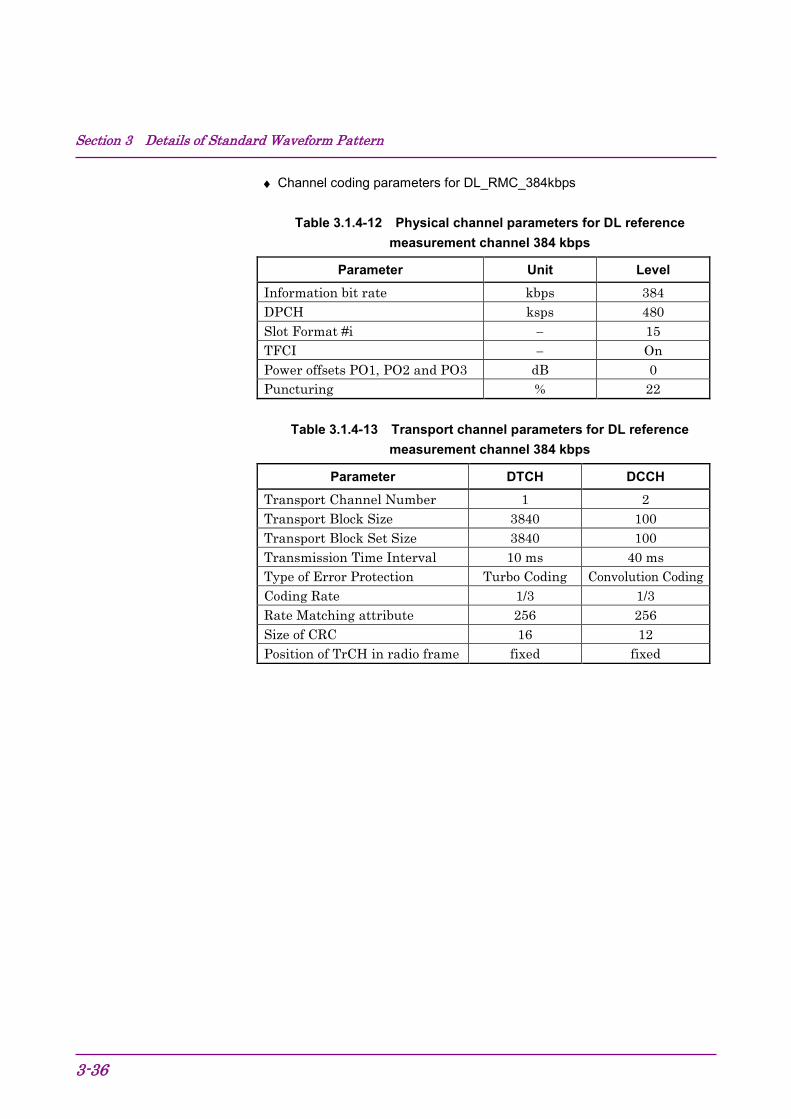
♦ Channel coding parameters for DL_RMC_384kbps
Table 3.1.4-12 Physical channel parameters for DL reference measurement channel 384 kbps
Parameter Unit Level Information bit rate kbps 384 DPCH ksps 480 Slot Format #i − 15 TFCI − On Power offsets PO1, PO2 and PO3 dB 0 Puncturing % 22
Table 3.1.4-13 Transport channel parameters for DL reference measurement channel 384 kbps
Parameter DTCH DCCH Transport Channel Number 1 2 Transport Block Size 3840 100 Transport Block Set Size 3840 100 Transmission Time Interval 10 ms 40 ms Type of Error Protection Turbo Coding Convolution Coding Coding Rate 1/3 1/3 Rate Matching attribute 256 256 Size of CRC 16 12 Position of TrCH in radio frame fixed fixed
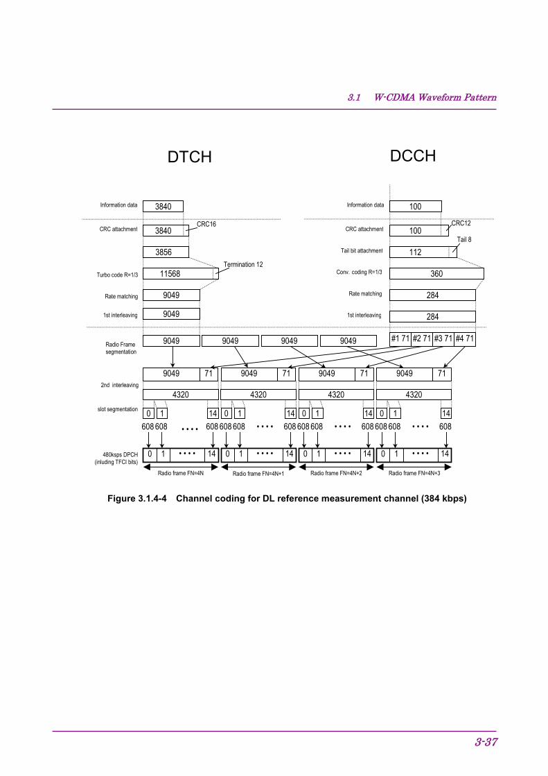
3.1 W-CDMA Waveform Pattern
3-37
9049
DCCHDTCH
480ksps DPCH(inluding TFCI bits)
Turbo code R=1/3
0 1 14
Radio frame FN=4N+1 Radio frame FN=4N+2 Radio frame FN=4N+3Radio frame FN=4N
Information data
CRC attachment
Rate matching
2nd interleaving4320
6080
• • • •
9049 71
4320 4320 4320
11568Termination 12
CRC163840
3840
112Tail 8
100
CRC12
1st interleaving
Radio Framesegmentation
slot segmentation
CRC attachment
Tail bit attachment
Conv. coding R=1/3
• • • • • • • • • • • •
• • • •
9049
9049 71 71 9049 71
#1 71
284
360
1 14 0 1 14
• • • •
0 1 14
• • • •
0 1 14
• • • •0 1 14 0 1 14 0 1 14
#2 71 #3 71 #4 71
284
Rate matching
1st interleaving
Information data
100
9049 9049 9049
9049
9049
3856
608 608 608 608 608 608 608 608 608 608 608
Figure 3.1.4-4 Channel coding for DL reference measurement channel (384 kbps)
Section 3 Details of Standard Waveform Pattern
3-38
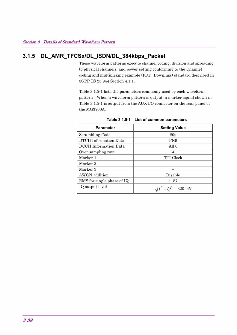
3.1.5 DL_AMR_TFCSx/DL_ISDN/DL_384kbps_Packet These waveform patterns execute channel coding, division and spreading to physical channels, and power setting conforming to the Channel coding and multiplexing example (FDD, Downlink) standard described in 3GPP TS 25.944 Section 4.1.1.
Table 3.1.5-1 lists the parameters commonly used by each waveform pattern When a waveform pattern is output, a marker signal shown in Table 3.1.5-1 is output from the AUX I/O connector on the rear panel of the MG3700A.
Table 3.1.5-1 List of common parameters
Parameter Setting Value
Scrambling Code 80H DTCH Information Data PN9 DCCH Information Data All 0 Over sampling rate 4 Marker 1 TTI Clock Marker 2 − Marker 3 − AWGN addition Disable RMS for single phase of IQ 1157 IQ output level 22 QI + = 320 mV
3.1 W-CDMA Waveform Pattern
3-39
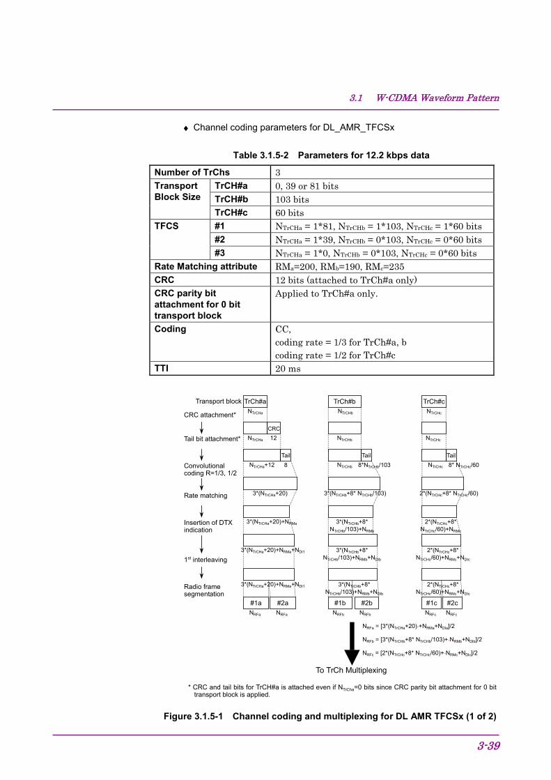
♦ Channel coding parameters for DL_AMR_TFCSx
Table 3.1.5-2 Parameters for 12.2 kbps data
Number of TrChs 3 Transport Block Size
TrCH#a 0, 39 or 81 bits TrCH#b 103 bits TrCH#c 60 bits
TFCS #1 NTrCHa = 1*81, NTrCHb = 1*103, NTrCHc = 1*60 bits #2 NTrCHa = 1*39, NTrCHb = 0*103, NTrCHc = 0*60 bits #3 NTrCHa = 1*0, NTrCHb = 0*103, NTrCHc = 0*60 bits
Rate Matching attribute RMa=200, RMb=190, RMc=235 CRC 12 bits (attached to TrCh#a only) CRC parity bit attachment for 0 bit transport block
Applied to TrCh#a only.
Coding CC, coding rate = 1/3 for TrCh#a, b coding rate = 1/2 for TrCh#c
TTI 20 ms
TrCh#aTransport block
CRC attachment*
CRC
Tail bit attachment*
Convolutionalcoding R=1/3, 1/2
Rate matching
NTrCHa
NTrCHa
3*(NTrCHa+20)
Tail8NTrCHa+12
3*(NTrCHa+20)+NRMa
1st interleaving
12
Radio framesegmentation
#1a
To TrCh Multiplexing
NRFa = [3*(NTrCHa+20) +NRMa+NDIa]/2
NRFb = [3*(NTrCHb+8* NTrCHb/103)+ NRMb+NDIb]/2
NRFc = [2*(NTrCHc+8* NTrCHc/60)+ NRMc+NDIc]/2
#2a
TrCh#bNTrCHb
NTrCHb
3*(NTrCHb+8* NTrCHb/103)
Tail8*NTrCHb/103NTrCHb
3*(NTrCHb+8*NTrCHb/103)+NRMb
#1b
TrCh#cNTrCHc
NTrCHc
2*(NTrCHc+8* NTrCHc/60)
Tail8* NTrCHc/60NTrCHc
2*(NTrCHc+8*NTrCHc/60)+NRMc
#1c #2c#2bNRFa NRFa NRFb NRFb NRFc NRFc
Insertion of DTXindication
3*(NTrCHa+20)+NRMa+NDI1 3*(NTrCHb+8*NTrCHb/103)+NRMb+NDIb
2*(NTrCHc+8*NTrCHc/60)+NRMc+NDIc
3*(NTrCHa+20)+NRMa+NDI1 3*(NTrCHb+8*NTrCHb/103)+NRMb+NDIb
2*(NTrCHc+8*NTrCHc/60)+NRMc+NDIc
* CRC and tail bits for TrCH#a is attached even if NTrCha=0 bits since CRC parity bit attachment for 0 bittransport block is applied.
Figure 3.1.5-1 Channel coding and multiplexing for DL AMR TFCSx (1 of 2)
Section 3 Details of Standard Waveform Pattern
3-40
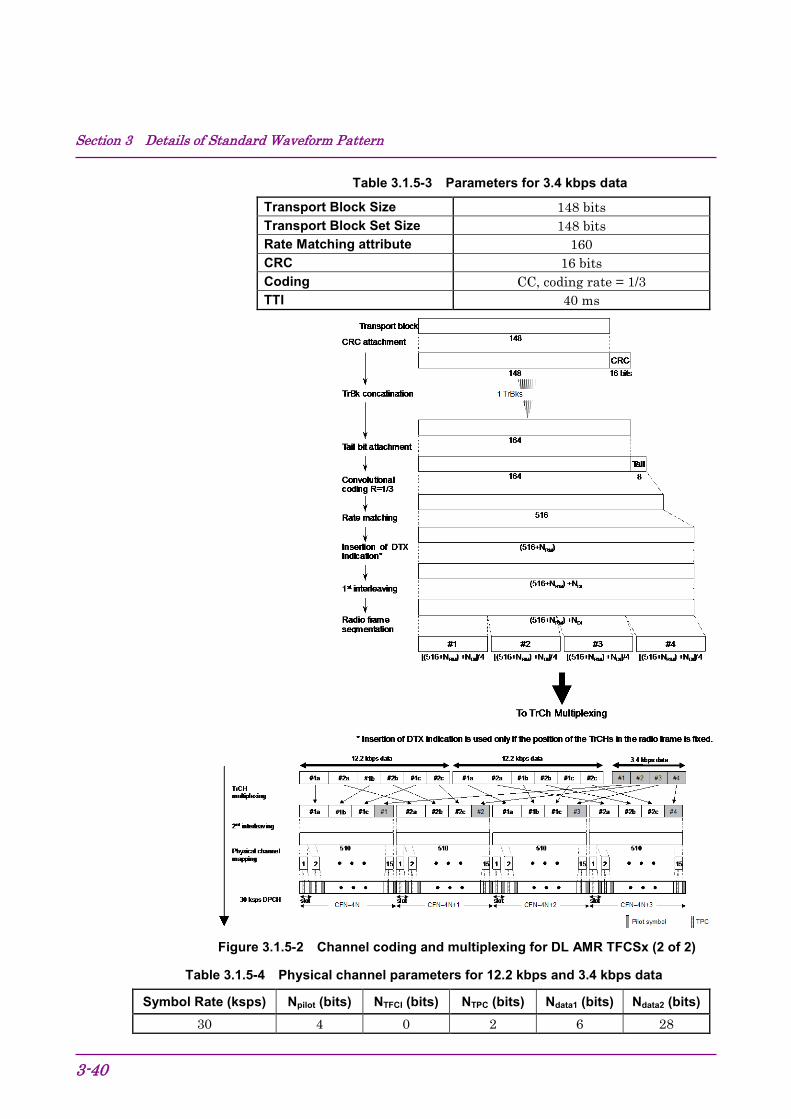
Table 3.1.5-3 Parameters for 3.4 kbps data
Transport Block Size 148 bits Transport Block Set Size 148 bits Rate Matching attribute 160 CRC 16 bits Coding CC, coding rate = 1/3 TTI 40 ms
Figure 3.1.5-2 Channel coding and multiplexing for DL AMR TFCSx (2 of 2)
Table 3.1.5-4 Physical channel parameters for 12.2 kbps and 3.4 kbps data
Symbol Rate (ksps) Npilot (bits) NTFCI (bits) NTPC (bits) Ndata1 (bits) Ndata2 (bits) 30 4 0 2 6 28
3.1 W-CDMA Waveform Pattern
3-41
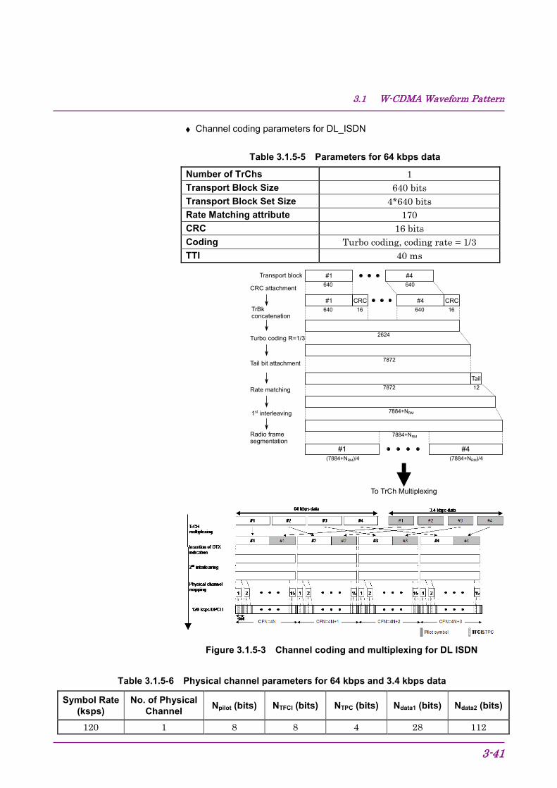
♦ Channel coding parameters for DL_ISDN
Table 3.1.5-5 Parameters for 64 kbps data
Number of TrChs 1 Transport Block Size 640 bits Transport Block Set Size 4*640 bits Rate Matching attribute 170 CRC 16 bits Coding Turbo coding, coding rate = 1/3 TTI 40 ms
#1Transport block
CRC attachment
#1 CRC
Turbo coding R=1/3
Rate matching
640
640 16
2624
#4
#4 CRC
640
640 16TrBkconcatenation
7884+NRM1st interleaving
7884+NRM
7872Tail bit attachment
Tail127872
Radio framesegmentation
#1 #4
To TrCh Multiplexing
(7884+NRM)/4 (7884+NRM)/4
Figure 3.1.5-3 Channel coding and multiplexing for DL ISDN
Table 3.1.5-6 Physical channel parameters for 64 kbps and 3.4 kbps data
Symbol Rate (ksps)
No. of Physical Channel Npilot (bits) NTFCI (bits) NTPC (bits) Ndata1 (bits) Ndata2 (bits)
120 1 8 8 4 28 112
Section 3 Details of Standard Waveform Pattern
3-42
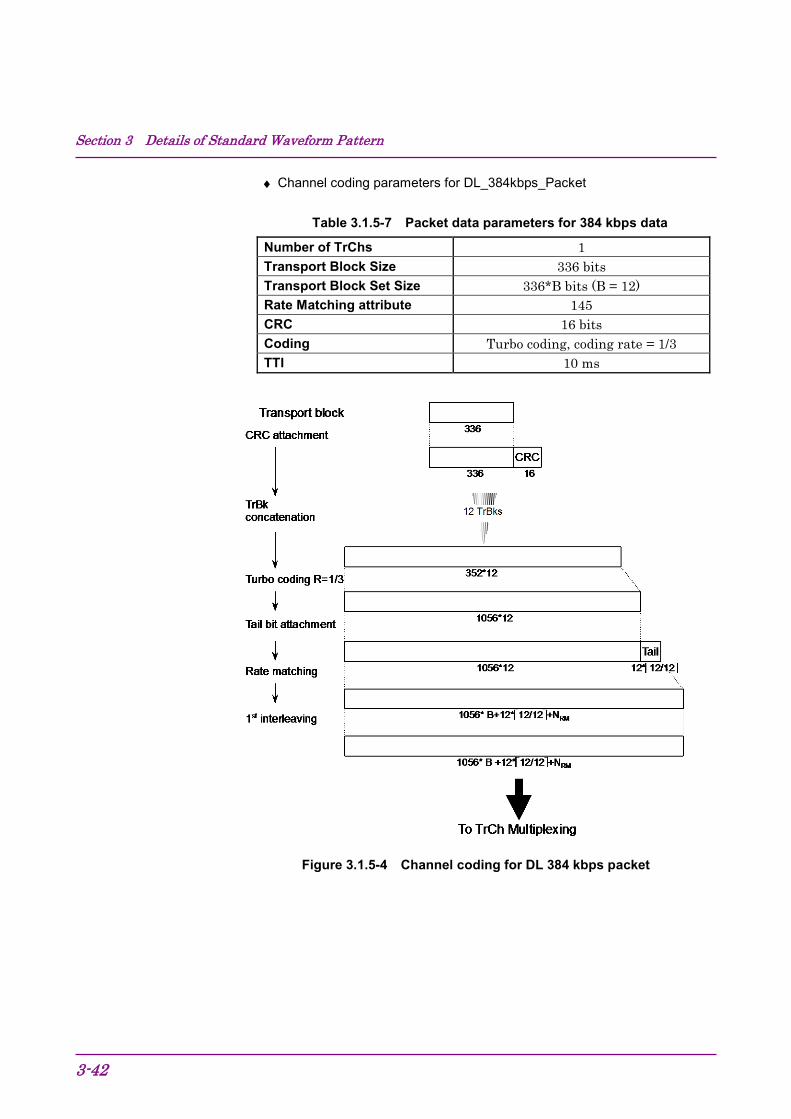
♦ Channel coding parameters for DL_384kbps_Packet
Table 3.1.5-7 Packet data parameters for 384 kbps data
Number of TrChs 1 Transport Block Size 336 bits Transport Block Set Size 336*B bits (B = 12) Rate Matching attribute 145 CRC 16 bits Coding Turbo coding, coding rate = 1/3 TTI 10 ms
Figure 3.1.5-4 Channel coding for DL 384 kbps packet
3.1 W-CDMA Waveform Pattern
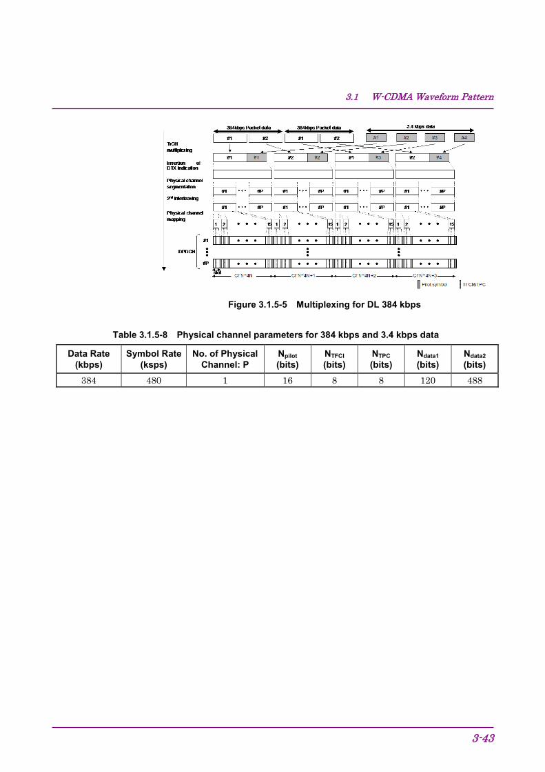
3-43
Figure 3.1.5-5 Multiplexing for DL 384 kbps
Table 3.1.5-8 Physical channel parameters for 384 kbps and 3.4 kbps data
Data Rate (kbps)
Symbol Rate (ksps)
No. of Physical Channel: P
Npilot (bits)
NTFCI (bits)
NTPC (bits)
Ndata1 (bits)
Ndata2 (bits)
384 480 1 16 8 8 120 488
Section 3 Details of Standard Waveform Pattern
3-44
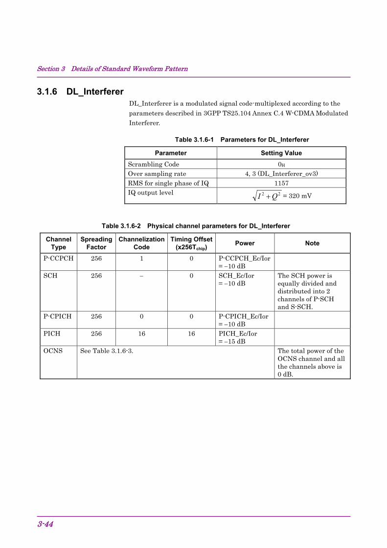
3.1.6 DL_Interferer DL_Interferer is a modulated signal code-multiplexed according to the parameters described in 3GPP TS25.104 Annex C.4 W-CDMA Modulated Interferer.
Table 3.1.6-1 Parameters for DL_Interferer
Parameter Setting Value Scrambling Code 0H Over sampling rate 4, 3 (DL_Interferer_ov3) RMS for single phase of IQ 1157 IQ output level 22 QI + = 320 mV
Table 3.1.6-2 Physical channel parameters for DL_Interferer
Channel Type
Spreading Factor
Channelization Code
Timing Offset (x256Tchip) Power Note
P-CCPCH 256 1 0 P-CCPCH_Ec/Ior = −10 dB
SCH 256 − 0 SCH_Ec/Ior = −10 dB
The SCH power is equally divided and distributed into 2 channels of P-SCH and S-SCH.
P-CPICH 256 0 0 P-CPICH_Ec/Ior = −10 dB
PICH 256 16 16 PICH_Ec/Ior = −15 dB
OCNS See Table 3.1.6-3. The total power of the OCNS channel and all the channels above is 0 dB.
3.1 W-CDMA Waveform Pattern
3-45
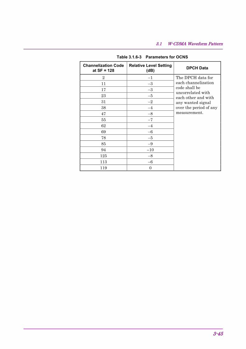
Table 3.1.6-3 Parameters for OCNS
Channelization Code at SF = 128
Relative Level Setting (dB) DPCH Data
2 −1 The DPCH data for each channelization code shall be uncorrelated with each other and with any wanted signal over the period of any measurement.
11 −3 17 −3 23 −5 31 −2 38 −4 47 −8 55 −7 62 −4 69 −6 78 −5 85 −9 94 −10 125 −8 113 −6 119 0
Section 3 Details of Standard Waveform Pattern
3-46
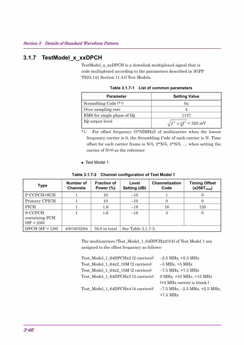
3.1.7 TestModel_x_xxDPCH TestModel_x_xxDPCH is a downlink multiplexed signal that is code-multiplexed according to the parameters described in 3GPP TS25.141 Section 11.4.0 Test Models.
Table 3.1.7-1 List of common parameters
Parameter Setting Value Scrambling Code (*1) 0H Over sampling rate 4 RMS for single phase of IQ 1157 IQ output level 22 QI + = 320 mV
*1: For offset frequency (5*N[MHz]) of multicarrier when the lowest frequency carrier is 0, the Scrambling Code of each carrier is N. Time offset for each carrier frame is N/5, 2*N/5, 3*N/5, … when setting the carrier of N=0 as the reference
♦ Test Model 1
Table 3.1.7-2 Channel configuration of Test Model 1
Type Number of Channels
Fraction of Power (%)
Level Setting (dB)
Channelization Code
Timing Offset (x256Tchip)
P-CCPCH+SCH 1 10 −10 1 0 Primary CPICH 1 10 −10 0 0 PICH 1 1.6 −18 16 120 S-CCPCH containing PCH (SF = 256)
1 1.6 −18 3 0
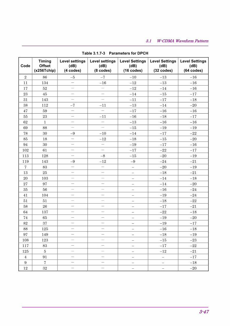
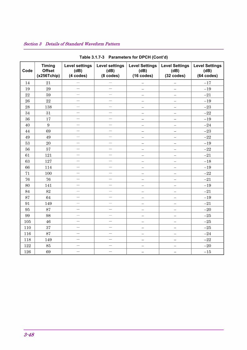
DPCH (SF = 128) 4/8/16/32/64 76.8 in total See Table 3.1.7-3. The multicarriers (Test_Model_1_64DPCHx2/3/4) of Test Model 1 are assigned to the offset frequency as follows:
Test_Model_1_64DPCHx2 (2 carriers): −2.5 MHz, +2.5 MHz Test_Model_1_64x2_10M (2 carriers): −5 MHz, +5 MHz Test_Model_1_64x2_15M (2 carriers): −7.5 MHz, +7.5 MHz Test_Model_1_64DPCHx3 (3 carriers): 0 MHz, +10 MHz, +15 MHz
(+5 MHz carrier is blank.) Test_Model_1_64DPCHx4 (4 carriers): −7.5 MHz, −2.5 MHz, +2.5 MHz,
+7.5 MHz
3.1 W-CDMA Waveform Pattern
3-47
Table 3.1.7-3 Parameters for DPCH
Code Timing Offset
(x256Tchip)
Level settings (dB)
(4 codes)
Level settings (dB)
(8 codes)
Level Settings (dB)
(16 codes)
Level Settings (dB)
(32 codes)
Level Settings (dB)
(64 codes) 2 86 −5 −7 −10 −13 −16 11 134 - −16 −12 −13 −16 17 52 - - −12 −14 −16 23 45 - - −14 −15 −17 31 143 - - −11 −17 −18 38 112 −7 −11 −13 −14 −20 47 59 - - −17 −16 −16 55 23 - −11 −16 −18 −17 62 1 - - −13 −16 −16 69 88 - - −15 −19 −19 78 30 −9 −10 −14 −17 −22 85 18 - −12 −18 −15 −20 94 30 - - −19 −17 −16 102 61 - - −17 −22 −17 113 128 - −8 −15 −20 −19 119 143 −9 −12 −9 −24 −21 7 83 - - − −20 −19 13 25 - - − −18 −21 20 103 - - − −14 −18 27 97 - - − −14 −20 35 56 - - − −16 −24 41 104 - - − −19 −24 51 51 - - − −18 −22 58 26 - - − −17 −21 64 137 - - − −22 −18 74 65 - - − −19 −20 82 37 - - − −19 −17 88 125 - - − −16 −18 97 149 - - − −18 −19 108 123 - - − −15 −23 117 83 - - − −17 −22 125 5 - - − −12 −21 4 91 - - − − −17 9 7 - - − − −18 12 32 - - − − −20
Section 3 Details of Standard Waveform Pattern
3-48
Table 3.1.7-3 Parameters for DPCH (Cont’d)
Code Timing Offset
(x256Tchip)
Level settings (dB)
(4 codes)
Level settings (dB)
(8 codes)
Level Settings (dB)
(16 codes)
Level Settings (dB)
(32 codes)
Level Settings (dB)
(64 codes) 14 21 - - − − −17 19 29 - - − − −19 22 59 - - − − −21 26 22 - - − − −19 28 138 - - − − −23 34 31 - - − − −22 36 17 - - − − −19 40 9 - - − − −24 44 69 - - − − −23 49 49 - - − − −22 53 20 - - − − −19 56 57 - - − − −22 61 121 - - − − −21 63 127 - - − − −18 66 114 - - − − −19 71 100 - - − − −22 76 76 - - − − −21 80 141 - - − − −19 84 82 - - − − −21 87 64 - - − − −19 91 149 - - − − −21 95 87 - - − − −20 99 98 - - − − −25 105 46 - - − − −25 110 37 - - − − −25 116 87 - - − − −24 118 149 - - − − −22 122 85 - - − − −20 126 69 - - − − −15
3.1 W-CDMA Waveform Pattern
3-49
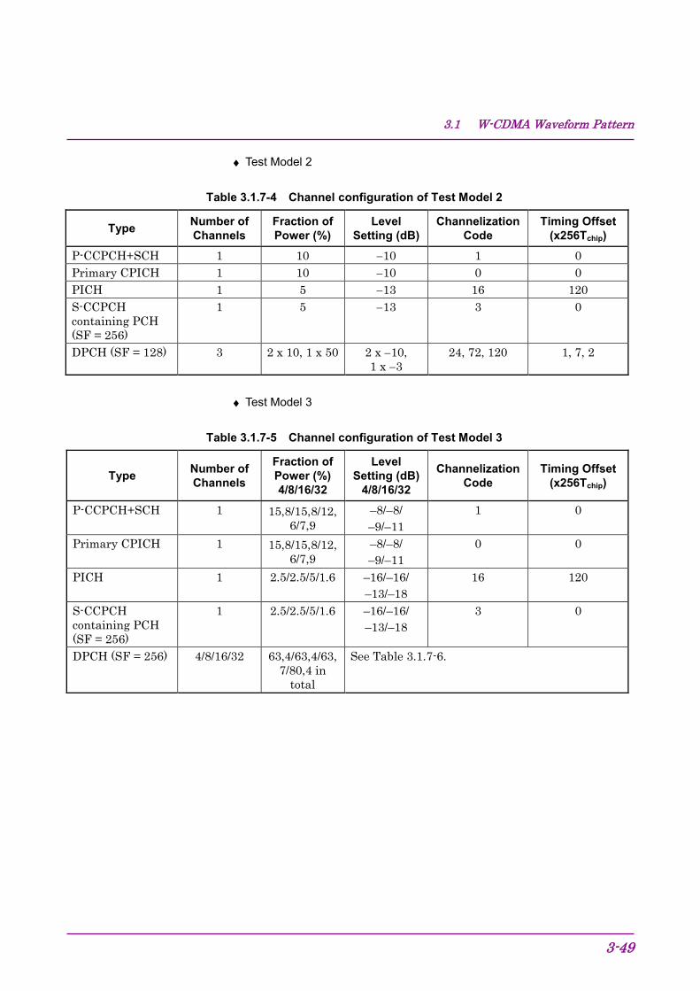
♦ Test Model 2
Table 3.1.7-4 Channel configuration of Test Model 2
Type Number of Channels
Fraction of Power (%)
Level Setting (dB)
Channelization Code
Timing Offset (x256Tchip)
P-CCPCH+SCH 1 10 −10 1 0 Primary CPICH 1 10 −10 0 0 PICH 1 5 −13 16 120 S-CCPCH containing PCH (SF = 256)
1 5 −13 3 0
DPCH (SF = 128) 3 2 x 10, 1 x 50 2 x −10, 1 x −3
24, 72, 120 1, 7, 2
♦ Test Model 3
Table 3.1.7-5 Channel configuration of Test Model 3
Type Number of Channels
Fraction of Power (%) 4/8/16/32
Level Setting (dB)
4/8/16/32
Channelization Code
Timing Offset (x256Tchip)
P-CCPCH+SCH 1 15,8/15,8/12,6/7,9
–8/–8/ –9/–11
1 0
Primary CPICH 1 15,8/15,8/12,6/7,9
–8/–8/ –9/–11
0 0
PICH 1 2.5/2.5/5/1.6 –16/–16/ –13/–18
16 120
S-CCPCH containing PCH (SF = 256)
1 2.5/2.5/5/1.6 –16/–16/ –13/–18
3 0
DPCH (SF = 256) 4/8/16/32 63,4/63,4/63,7/80,4 in
total
See Table 3.1.7-6.
Section 3 Details of Standard Waveform Pattern
3-50
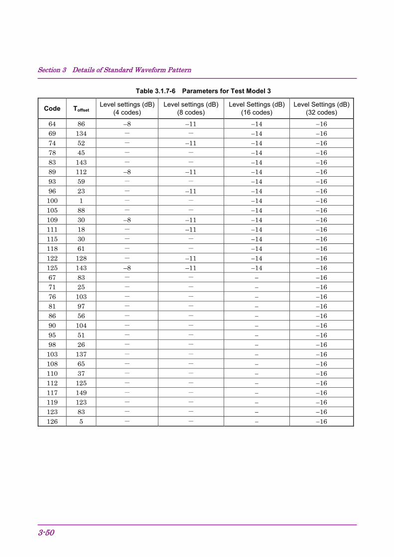
Table 3.1.7-6 Parameters for Test Model 3
Code Toffset Level settings (dB)
(4 codes) Level settings (dB)
(8 codes) Level Settings (dB)
(16 codes) Level Settings (dB)
(32 codes)
64 86 –8 –11 −14 −16 69 134 - - −14 −16 74 52 - –11 −14 −16 78 45 - - −14 −16 83 143 - - −14 −16 89 112 –8 –11 −14 −16 93 59 - - −14 −16 96 23 - –11 −14 −16 100 1 - - −14 −16 105 88 - - −14 −16 109 30 –8 –11 −14 −16 111 18 - –11 −14 −16 115 30 - - −14 −16 118 61 - - −14 −16 122 128 - –11 −14 −16 125 143 –8 –11 −14 −16 67 83 - - − −16 71 25 - - − −16 76 103 - - − −16 81 97 - - − −16 86 56 - - − −16 90 104 - - − −16 95 51 - - − −16 98 26 - - − −16 103 137 - - − −16 108 65 - - − −16 110 37 - - − −16 112 125 - - − −16 117 149 - - − −16 119 123 - - − −16 123 83 - - − −16 126 5 - - − −16
3.1 W-CDMA Waveform Pattern
3-51
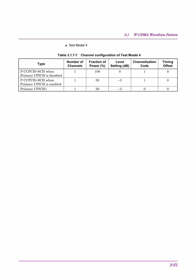
♦ Test Model 4
Table 3.1.7-7 Channel configuration of Test Model 4
Type Number of Channels
Fraction of Power (%)
Level Setting (dB)
Channelization Code
Timing Offset
P-CCPCH+SCH when Primary CPICH is disabled
1 100 0 1 0
P-CCPCH+SCH when Primary CPICH is enabled
1 50 –3 1 0
Primary CPICH1 1 50 –3 0 0
Section 3 Details of Standard Waveform Pattern
3-52
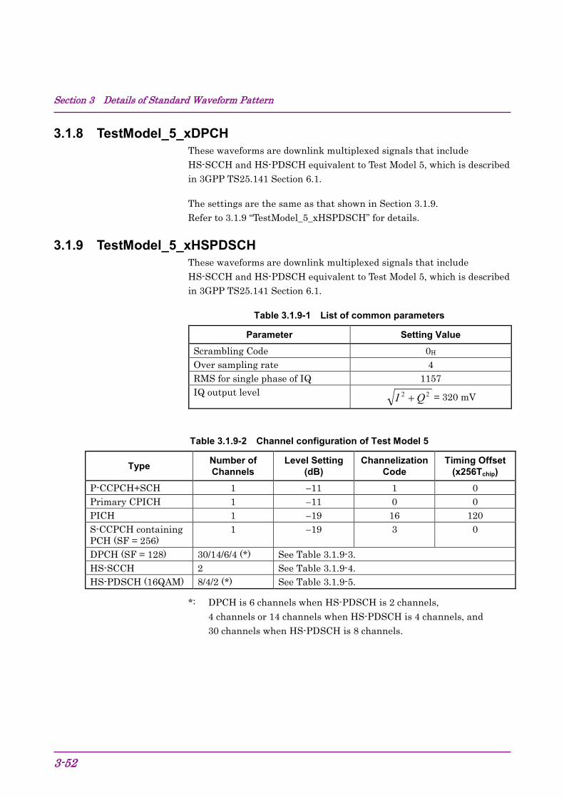
3.1.8 TestModel_5_xDPCH These waveforms are downlink multiplexed signals that include HS-SCCH and HS-PDSCH equivalent to Test Model 5, which is described in 3GPP TS25.141 Section 6.1.
The settings are the same as that shown in Section 3.1.9. Refer to 3.1.9 “TestModel_5_xHSPDSCH” for details.
3.1.9 TestModel_5_xHSPDSCH These waveforms are downlink multiplexed signals that include HS-SCCH and HS-PDSCH equivalent to Test Model 5, which is described in 3GPP TS25.141 Section 6.1.
Table 3.1.9-1 List of common parameters
Parameter Setting Value Scrambling Code 0H Over sampling rate 4 RMS for single phase of IQ 1157 IQ output level 22 QI + = 320 mV
Table 3.1.9-2 Channel configuration of Test Model 5
Type Number of Channels
Level Setting (dB)
Channelization Code
Timing Offset (x256Tchip)
P-CCPCH+SCH 1 −11 1 0 Primary CPICH 1 −11 0 0 PICH 1 −19 16 120 S-CCPCH containing PCH (SF = 256)
1 −19 3 0
DPCH (SF = 128) 30/14/6/4 (*) See Table 3.1.9-3. HS-SCCH 2 See Table 3.1.9-4. HS-PDSCH (16QAM) 8/4/2 (*) See Table 3.1.9-5.
*: DPCH is 6 channels when HS-PDSCH is 2 channels, 4 channels or 14 channels when HS-PDSCH is 4 channels, and 30 channels when HS-PDSCH is 8 channels.
3.1 W-CDMA Waveform Pattern
3-53
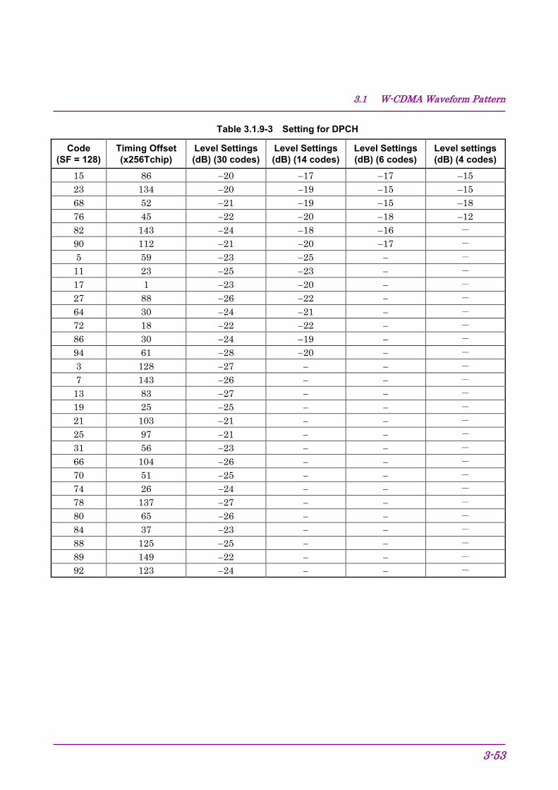
Table 3.1.9-3 Setting for DPCH
Code (SF = 128)
Timing Offset (x256Tchip)
Level Settings (dB) (30 codes)
Level Settings (dB) (14 codes)
Level Settings (dB) (6 codes)
Level settings (dB) (4 codes)
15 86 −20 −17 −17 –15 23 134 −20 −19 −15 –15 68 52 −21 −19 −15 –18 76 45 −22 −20 −18 –12 82 143 −24 −18 −16 - 90 112 −21 −20 −17 - 5 59 −23 −25 − - 11 23 −25 −23 − - 17 1 −23 −20 − - 27 88 −26 −22 − - 64 30 −24 −21 − - 72 18 −22 −22 − - 86 30 −24 −19 − - 94 61 −28 −20 − - 3 128 −27 − − - 7 143 −26 − − - 13 83 −27 − − - 19 25 −25 − − - 21 103 −21 − − - 25 97 −21 − − - 31 56 −23 − − - 66 104 −26 − − - 70 51 −25 − − - 74 26 −24 − − - 78 137 −27 − − - 80 65 −26 − − - 84 37 −23 − − - 88 125 −25 − − - 89 149 −22 − − - 92 123 −24 − − -
Section 3 Details of Standard Waveform Pattern
3-54
Table 3.1.9-4 Settings for HS-SCCH
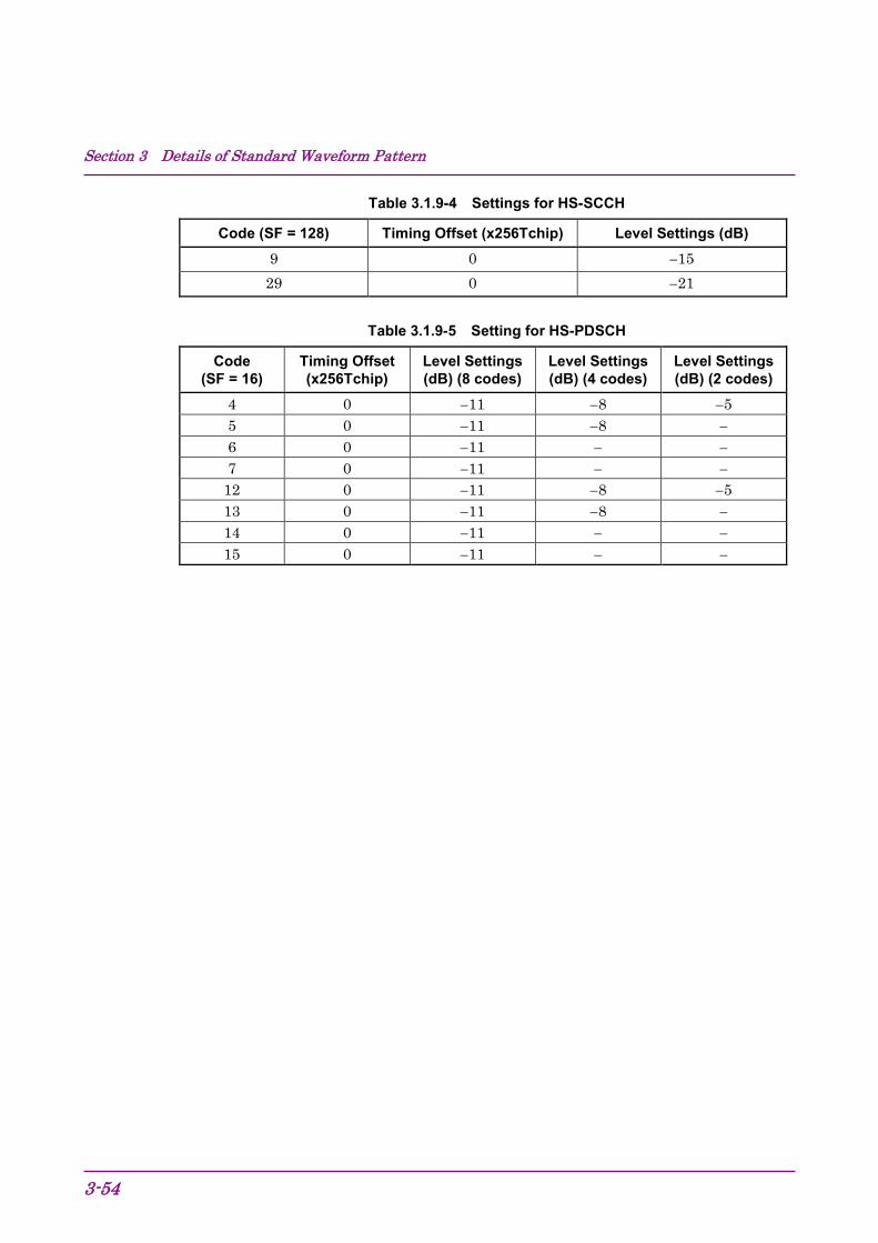
Code (SF = 128) Timing Offset (x256Tchip) Level Settings (dB) 9 0 −15 29 0 −21
Table 3.1.9-5 Setting for HS-PDSCH
Code (SF = 16)
Timing Offset (x256Tchip)
Level Settings (dB) (8 codes)
Level Settings (dB) (4 codes)
Level Settings (dB) (2 codes)
4 0 −11 −8 −5 5 0 −11 −8 − 6 0 −11 − − 7 0 −11 − −
12 0 −11 −8 −5 13 0 −11 −8 − 14 0 −11 − − 15 0 −11 − −
3.1 W-CDMA Waveform Pattern
3-55
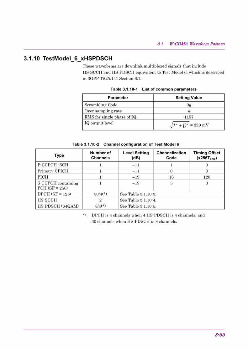
3.1.10 TestModel_6_xHSPDSCH These waveforms are downlink multiplexed signals that include HS-SCCH and HS-PDSCH equivalent to Test Model 6, which is described in 3GPP TS25.141 Section 6.1.
Table 3.1.10-1 List of common parameters
Parameter Setting Value Scrambling Code 0H Over sampling rate 4 RMS for single phase of IQ 1157 IQ output level 22 QI + = 320 mV
Table 3.1.10-2 Channel configuration of Test Model 6
Type Number of Channels
Level Setting (dB)
Channelization Code
Timing Offset (x256Tchip)
P-CCPCH+SCH 1 −11 1 0 Primary CPICH 1 −11 0 0 PICH 1 −19 16 120 S-CCPCH containing PCH (SF = 256)
1 −19 3 0
DPCH (SF = 128) 30/4(*) See Table 3.1.10-3. HS-SCCH 2 See Table 3.1.10-4. HS-PDSCH (64QAM) 8/4(*) See Table 3.1.10-5.
*: DPCH is 4 channels when 4 HS-PDSCH is 4 channels, and 30 channels when HS-PDSCH is 8 channels.
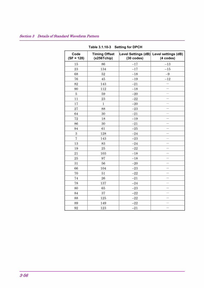
Section 3 Details of Standard Waveform Pattern
3-56
Table 3.1.10-3 Setting for DPCH
Code (SF = 128)
Timing Offset (x256Tchip)
Level Settings (dB) (30 codes)
Level settings (dB) (4 codes)
15 86 –17 –13 23 134 –17 –15 68 52 –18 –9 76 45 –19 –12 82 143 –21 - 90 112 –18 - 5 59 –20 - 11 23 –22 - 17 1 –20 - 27 88 –23 - 64 30 –21 - 72 18 –19 - 86 30 –21 - 94 61 –25 - 3 128 –24 - 7 143 –23 - 13 83 –24 - 19 25 –22 - 21 103 –18 - 25 97 –18 - 31 56 –20 - 66 104 –23 - 70 51 –22 - 74 26 –21 - 78 137 –24 - 80 65 –23 - 84 37 –22 - 88 125 –22 - 89 149 –22 - 92 123 –21 -
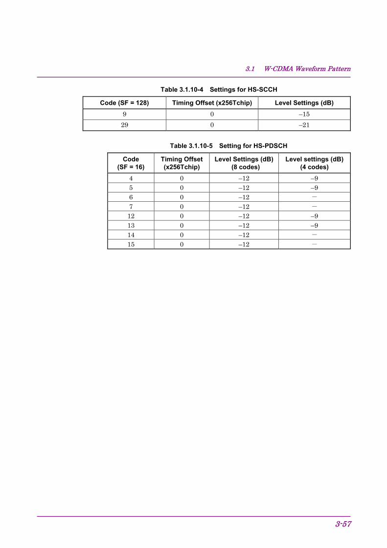
3.1 W-CDMA Waveform Pattern
3-57
Table 3.1.10-4 Settings for HS-SCCH
Code (SF = 128) Timing Offset (x256Tchip) Level Settings (dB) 9 0 –15 29 0 –21
Table 3.1.10-5 Setting for HS-PDSCH
Code (SF = 16)
Timing Offset (x256Tchip)
Level Settings (dB) (8 codes)
Level settings (dB) (4 codes)
4 0 –12 –9 5 0 –12 –9 6 0 –12 - 7 0 –12 - 12 0 –12 –9 13 0 –12 –9 14 0 –12 - 15 0 –12 -
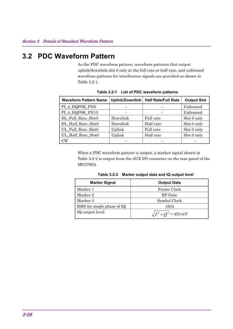
Section 3 Details of Standard Waveform Pattern
3-58
3.2 PDC Waveform Pattern As the PDC waveform pattern, waveform patterns that output uplink/downlink slot 0 only at the full rate or half rate, and unframed waveform patterns for interference signals are provided as shown in Table 3.2-1.
Table 3.2-1 List of PDC waveform patterns
Waveform Pattern Name Uplink/Downlink Half Rate/Full Rate Output Slot PI_4_DQPSK_PN9 − − Unframed PI_4_DQPSK_PN15 − − Unframed DL_Full_Rate_Slot0 Downlink Full rate Slot 0 only DL_Half_Rate_Slot0 Downlink Half rate Slot 0 only UL_Full_Rate_Slot0 Uplink Full rate Slot 0 only UL_Half_Rate_Slot0 Uplink Half rate Slot 0 only CW − − −
When a PDC waveform pattern is output, a marker signal shown in Table 3.2-2 is output from the AUX I/O connector on the rear panel of the MG3700A.
Table 3.2-2 Marker output data and IQ output level
Marker Signal Output Data Marker 1 Frame Clock Marker 2 RF Gate Marker 3 Symbol Clock RMS for single phase of IQ 1634 IQ output level 22 QI + = 453 mV
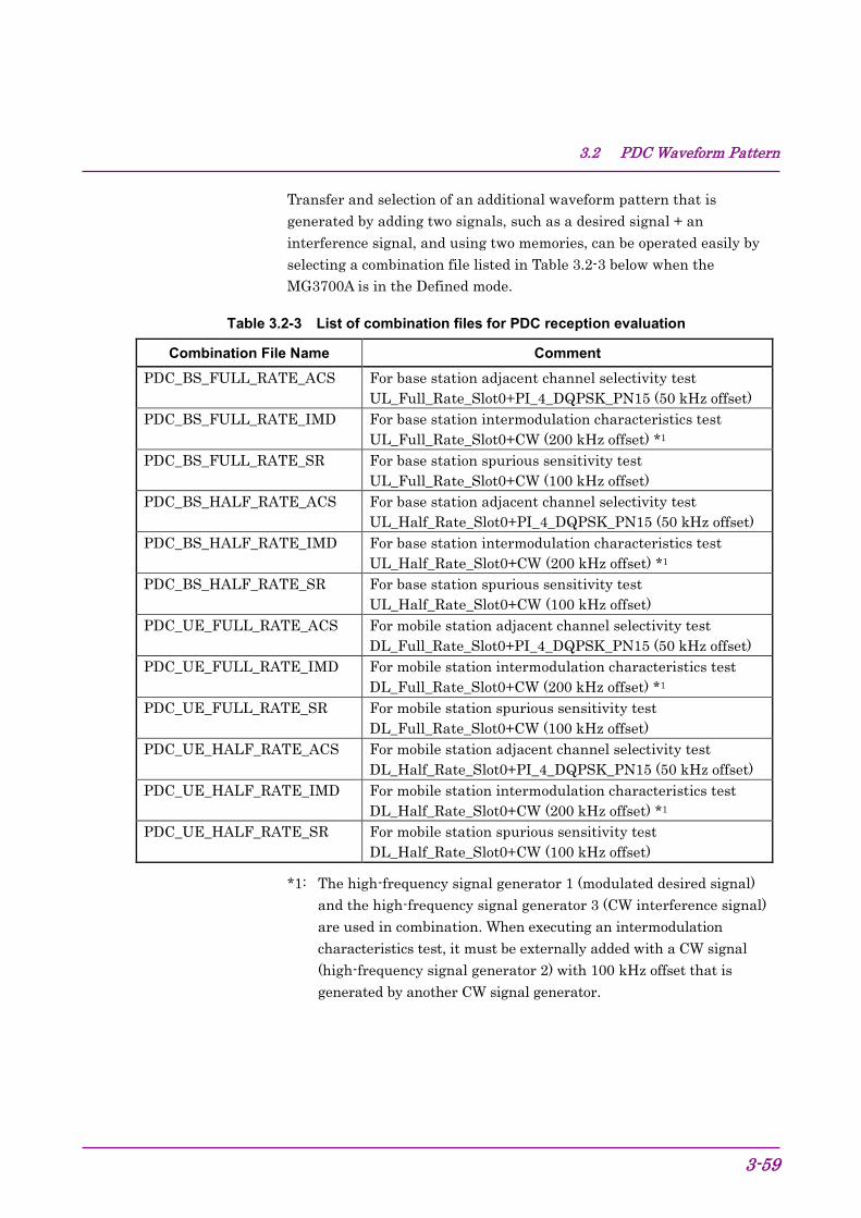
3.2 PDC Waveform Pattern
3-59
Transfer and selection of an additional waveform pattern that is generated by adding two signals, such as a desired signal + an interference signal, and using two memories, can be operated easily by selecting a combination file listed in Table 3.2-3 below when the MG3700A is in the Defined mode.
Table 3.2-3 List of combination files for PDC reception evaluation
Combination File Name Comment PDC_BS_FULL_RATE_ACS For base station adjacent channel selectivity test
UL_Full_Rate_Slot0+PI_4_DQPSK_PN15 (50 kHz offset) PDC_BS_FULL_RATE_IMD For base station intermodulation characteristics test
UL_Full_Rate_Slot0+CW (200 kHz offset) *1 PDC_BS_FULL_RATE_SR For base station spurious sensitivity test
UL_Full_Rate_Slot0+CW (100 kHz offset) PDC_BS_HALF_RATE_ACS For base station adjacent channel selectivity test
UL_Half_Rate_Slot0+PI_4_DQPSK_PN15 (50 kHz offset) PDC_BS_HALF_RATE_IMD For base station intermodulation characteristics test
UL_Half_Rate_Slot0+CW (200 kHz offset) *1 PDC_BS_HALF_RATE_SR For base station spurious sensitivity test
UL_Half_Rate_Slot0+CW (100 kHz offset) PDC_UE_FULL_RATE_ACS For mobile station adjacent channel selectivity test
DL_Full_Rate_Slot0+PI_4_DQPSK_PN15 (50 kHz offset) PDC_UE_FULL_RATE_IMD For mobile station intermodulation characteristics test
DL_Full_Rate_Slot0+CW (200 kHz offset) *1 PDC_UE_FULL_RATE_SR For mobile station spurious sensitivity test
DL_Full_Rate_Slot0+CW (100 kHz offset) PDC_UE_HALF_RATE_ACS For mobile station adjacent channel selectivity test
DL_Half_Rate_Slot0+PI_4_DQPSK_PN15 (50 kHz offset) PDC_UE_HALF_RATE_IMD For mobile station intermodulation characteristics test
DL_Half_Rate_Slot0+CW (200 kHz offset) *1 PDC_UE_HALF_RATE_SR For mobile station spurious sensitivity test
DL_Half_Rate_Slot0+CW (100 kHz offset)
*1: The high-frequency signal generator 1 (modulated desired signal) and the high-frequency signal generator 3 (CW interference signal) are used in combination. When executing an intermodulation characteristics test, it must be externally added with a CW signal (high-frequency signal generator 2) with 100 kHz offset that is generated by another CW signal generator.
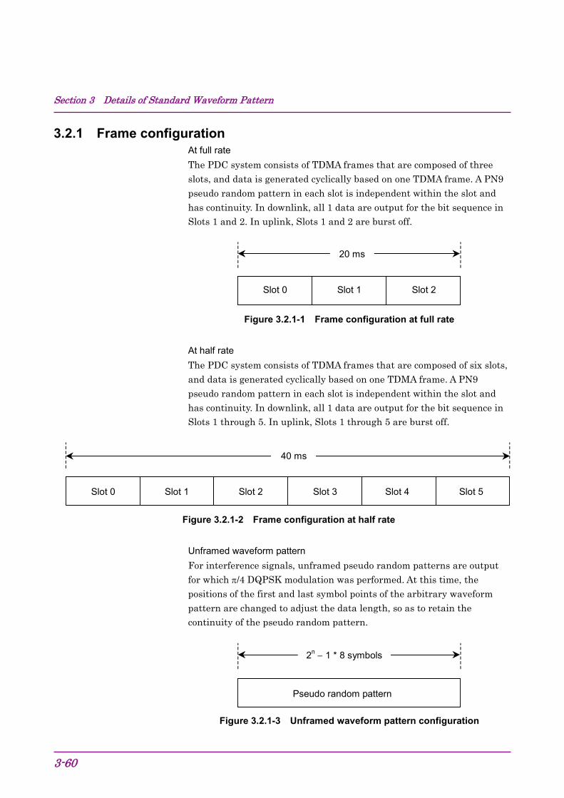
Section 3 Details of Standard Waveform Pattern
3-60
3.2.1 Frame configuration At full rate The PDC system consists of TDMA frames that are composed of three slots, and data is generated cyclically based on one TDMA frame. A PN9 pseudo random pattern in each slot is independent within the slot and has continuity. In downlink, all 1 data are output for the bit sequence in Slots 1 and 2. In uplink, Slots 1 and 2 are burst off.
20 ms
Slot 0 Slot 1 Slot 2
Figure 3.2.1-1 Frame configuration at full rate
At half rate The PDC system consists of TDMA frames that are composed of six slots, and data is generated cyclically based on one TDMA frame. A PN9 pseudo random pattern in each slot is independent within the slot and has continuity. In downlink, all 1 data are output for the bit sequence in Slots 1 through 5. In uplink, Slots 1 through 5 are burst off.
40 ms
Slot 0 Slot 1 Slot 5 Slot 4 Slot 3 Slot 2
Figure 3.2.1-2 Frame configuration at half rate
Unframed waveform pattern For interference signals, unframed pseudo random patterns are output for which π/4 DQPSK modulation was performed. At this time, the positions of the first and last symbol points of the arbitrary waveform pattern are changed to adjust the data length, so as to retain the continuity of the pseudo random pattern.
Pseudo random pattern
2n − 1 * 8 symbols
Figure 3.2.1-3 Unframed waveform pattern configuration
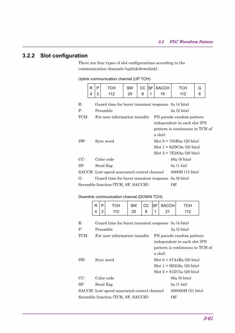
3.2 PDC Waveform Pattern
3-61
3.2.2 Slot configuration There are four types of slot configurations according to the communication channels (uplink/downlink).
Uplink communication channel (UP TCH)
R4
TCH112
G6
P2
SACCH15
SF1
CC8
SW20
TCH112
R: Guard time for burst transient response 0H (4 bits) P: Preamble 2H (2 bits) TCH: For user information transfer PN pseudo random pattern
independent in each slot (PN pattern is continuous in TCH of a slot).
SW: Sync word Slot 0 = 785B4H (20 bits) Slot 1 = 62DC9H (20 bits) Slot 2 = 7E28AH (20 bits)
CC: Color code 00H (8 bits) SF: Steal flag 0H (1 bit) SACCH: Low-speed associated control channel 0000H (15 bits) G: Guard time for burst transient response 0H (6 bits) Scramble function (TCH, SF, SACCH): Off
Downlink communication channel (DOWN TCH)
R4
TCH112
P2
SACCH21
SF1
CC8
SW20
TCH112
R: Guard time for burst transient response 0H (4 bits) P: Preamble 2H (2 bits) TCH: For user information transfer PN pseudo random pattern
independent in each slot (PN pattern is continuous in TCH of a slot).
SW: Sync word Slot 0 = 87A4BH (20 bits) Slot 1 = 9D236H (20 bits) Slot 2 = 81D75H (20 bits)
CC: Color code 00H (8 bits) SF: Steal flag 0H (1 bit) SACCH: Low-speed associated control channel 000000H (21 bits) Scramble function (TCH, SF, SACCH): Off
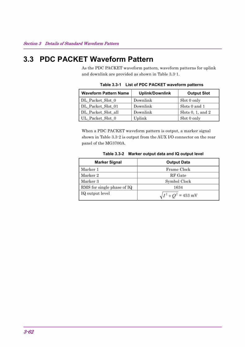
Section 3 Details of Standard Waveform Pattern
3-62
3.3 PDC PACKET Waveform Pattern As the PDC PACKET waveform pattern, waveform patterns for uplink and downlink are provided as shown in Table 3.3-1.
Table 3.3-1 List of PDC PACKET waveform patterns
Waveform Pattern Name Uplink/Downlink Output Slot DL_Packet_Slot_0 Downlink Slot 0 only DL_Packet_Slot_01 Downlink Slots 0 and 1 DL_Packet_Slot_all Downlink Slots 0, 1, and 2 UL_Packet_Slot_0 Uplink Slot 0 only When a PDC PACKET waveform pattern is output, a marker signal shown in Table 3.3-2 is output from the AUX I/O connector on the rear panel of the MG3700A.
Table 3.3-2 Marker output data and IQ output level
Marker Signal Output Data
Marker 1 Frame Clock Marker 2 RF Gate Marker 3 Symbol Clock RMS for single phase of IQ 1634 IQ output level 22 QI + = 453 mV
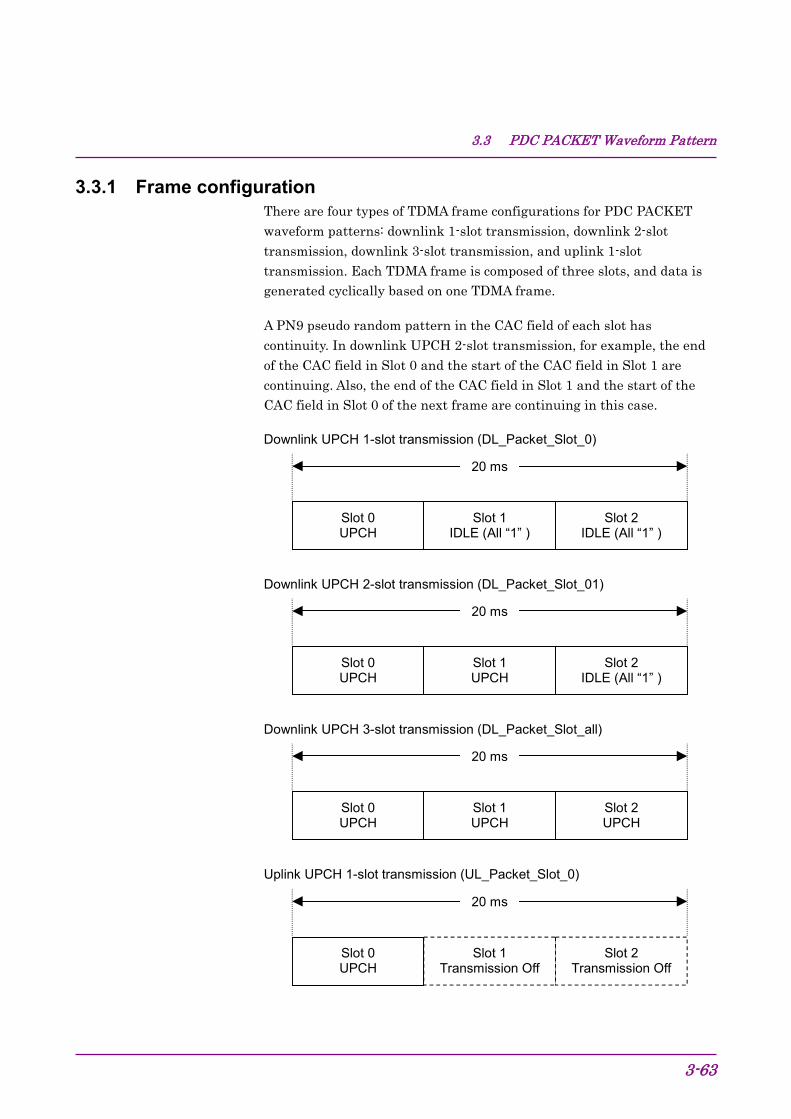
3.3 PDC PACKET Waveform Pattern
3-63
3.3.1 Frame configuration There are four types of TDMA frame configurations for PDC PACKET waveform patterns: downlink 1-slot transmission, downlink 2-slot transmission, downlink 3-slot transmission, and uplink 1-slot transmission. Each TDMA frame is composed of three slots, and data is generated cyclically based on one TDMA frame.
A PN9 pseudo random pattern in the CAC field of each slot has continuity. In downlink UPCH 2-slot transmission, for example, the end of the CAC field in Slot 0 and the start of the CAC field in Slot 1 are continuing. Also, the end of the CAC field in Slot 1 and the start of the CAC field in Slot 0 of the next frame are continuing in this case.
Downlink UPCH 1-slot transmission (DL_Packet_Slot_0)
Slot 0 UPCH
Slot 1 IDLE (All “1” )
Slot 2 IDLE (All “1” )
20 ms
Downlink UPCH 2-slot transmission (DL_Packet_Slot_01)
Slot 0 UPCH
Slot 1 UPCH
Slot 2 IDLE (All “1” )
20 ms
Downlink UPCH 3-slot transmission (DL_Packet_Slot_all)
Slot 0 UPCH
Slot 1 UPCH
Slot 2 UPCH
20 ms
Uplink UPCH 1-slot transmission (UL_Packet_Slot_0)
Slot 0 UPCH
Slot 1 Transmission Off
Slot 2 Transmission Off
20 ms
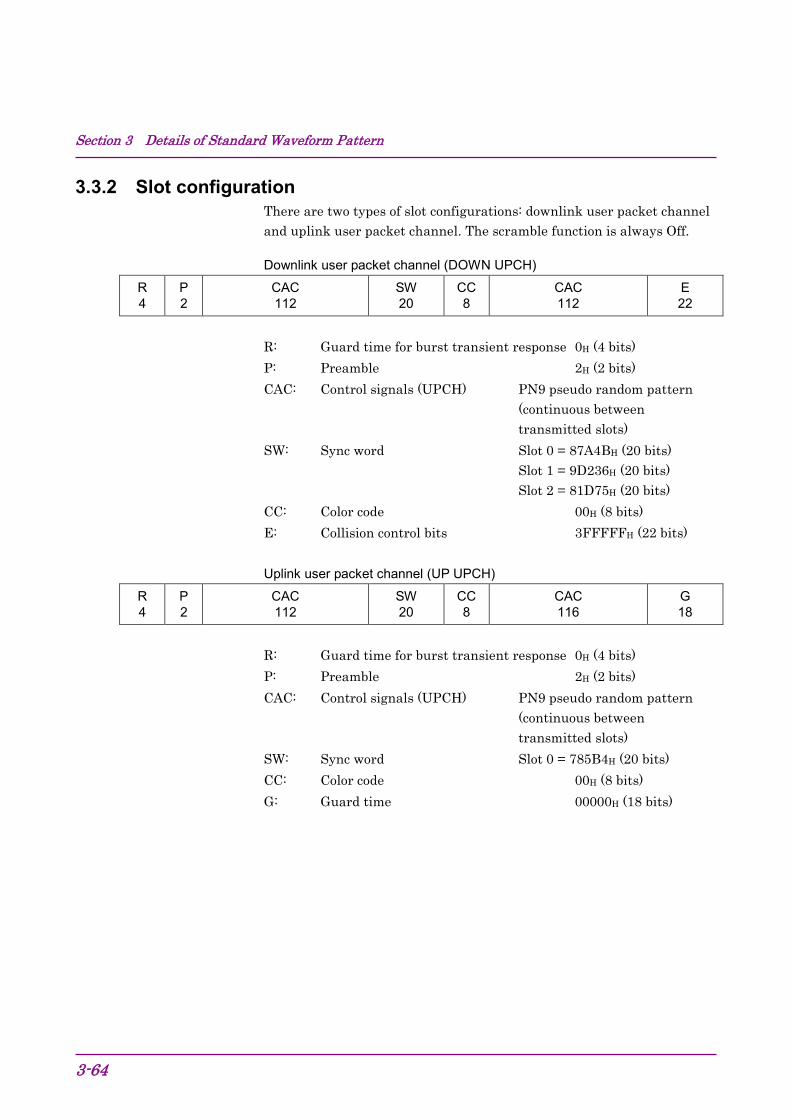
Section 3 Details of Standard Waveform Pattern
3-64
3.3.2 Slot configuration There are two types of slot configurations: downlink user packet channel and uplink user packet channel. The scramble function is always Off.
Downlink user packet channel (DOWN UPCH)
R 4
P 2
CAC 112
SW 20
CC 8
CAC 112
E 22
R: Guard time for burst transient response 0H (4 bits) P: Preamble 2H (2 bits) CAC: Control signals (UPCH) PN9 pseudo random pattern
(continuous between transmitted slots)
SW: Sync word Slot 0 = 87A4BH (20 bits) Slot 1 = 9D236H (20 bits) Slot 2 = 81D75H (20 bits)
CC: Color code 00H (8 bits) E: Collision control bits 3FFFFFH (22 bits)
Uplink user packet channel (UP UPCH)
R 4
P 2
CAC 112
SW 20
CC 8
CAC 116
G 18
R: Guard time for burst transient response 0H (4 bits) P: Preamble 2H (2 bits) CAC: Control signals (UPCH) PN9 pseudo random pattern
(continuous between transmitted slots)
SW: Sync word Slot 0 = 785B4H (20 bits) CC: Color code 00H (8 bits) G: Guard time 00000H (18 bits)
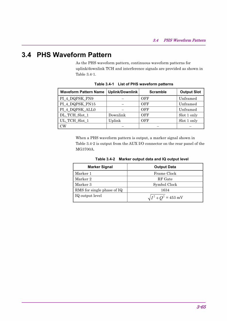
3.4 PHS Waveform Pattern
3-65
3.4 PHS Waveform Pattern As the PHS waveform pattern, continuous waveform patterns for uplink/downlink TCH and interference signals are provided as shown in Table 3.4-1.
Table 3.4-1 List of PHS waveform patterns
Waveform Pattern Name Uplink/Downlink Scramble Output Slot PI_4_DQPSK_PN9 − OFF Unframed PI_4_DQPSK_PN15 − OFF Unframed PI_4_DQPSK_ALL0 − OFF Unframed DL_TCH_Slot_1 Downlink OFF Slot 1 only UL_TCH_Slot_1 Uplink OFF Slot 1 only CW − − −
When a PHS waveform pattern is output, a marker signal shown in Table 3.4-2 is output from the AUX I/O connector on the rear panel of the MG3700A.
Table 3.4-2 Marker output data and IQ output level
Marker Signal Output Data Marker 1 Frame Clock Marker 2 RF Gate Marker 3 Symbol Clock RMS for single phase of IQ 1634 IQ output level 22 QI + = 453 mV
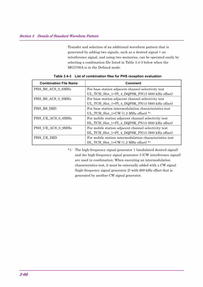
Section 3 Details of Standard Waveform Pattern
3-66
Transfer and selection of an additional waveform pattern that is generated by adding two signals, such as a desired signal + an interference signal, and using two memories, can be operated easily by selecting a combination file listed in Table 3.4-3 below when the MG3700A is in the Defined mode.
Table 3.4-3 List of combination files for PHS reception evaluation
Combination File Name Comment PHS_BS_ACS_0_6MHz For base station adjacent channel selectivity test
UL_TCH_Slot_1+PI_4_DQPSK_PN15 (600 kHz offset) PHS_BS_ACS_0_9MHz For base station adjacent channel selectivity test
UL_TCH_Slot_1+PI_4_DQPSK_PN15 (900 kHz offset) PHS_BS_IMD For base station intermodulation characteristics test
UL_TCH_Slot_1+CW (1.2 MHz offset) *1 PHS_UE_ACS_0_6MHz For mobile station adjacent channel selectivity test
DL_TCH_Slot_1+PI_4_DQPSK_PN15 (600 kHz offset) PHS_UE_ACS_0_9MHz For mobile station adjacent channel selectivity test
DL_TCH_Slot_1+PI_4_DQPSK_PN15 (900 kHz offset) PHS_UE_IMD For mobile station intermodulation characteristics test
DL_TCH_Slot_1+CW (1.2 MHz offset) *1
*1: The high-frequency signal generator 1 (modulated desired signal) and the high-frequency signal generator 3 (CW interference signal) are used in combination. When executing an intermodulation characteristics test, it must be externally added with a CW signal (high-frequency signal generator 2) with 600-kHz offset that is generated by another CW signal generator.
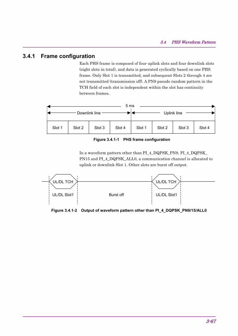
3.4 PHS Waveform Pattern
3-67
3.4.1 Frame configuration Each PHS frame is composed of four uplink slots and four downlink slots (eight slots in total), and data is generated cyclically based on one PHS frame. Only Slot 1 is transmitted, and subsequent Slots 2 through 4 are not transmitted (transmission off). A PN9 pseudo random pattern in the TCH field of each slot is independent within the slot has continuity between frames.
5 ms
Downlink line Uplink line
Slot 1 Slot 2 Slot 3 Slot 4 Slot 1 Slot 2 Slot 3 Slot 4
Figure 3.4.1-1 PHS frame configuration
In a waveform pattern other than PI_4_DQPSK_PN9, PI_4_DQPSK_ PN15 and PI_4_DQPSK_ALL0, a communication channel is allocated to uplink or downlink Slot 1. Other slots are burst off output.
UL/DL TCH UL/DL TCH
UL/DL Slot1 Burst off UL/DL Slot1
Figure 3.4.1-2 Output of waveform pattern other than PI_4_DQPSK_PN9/15/ALL0
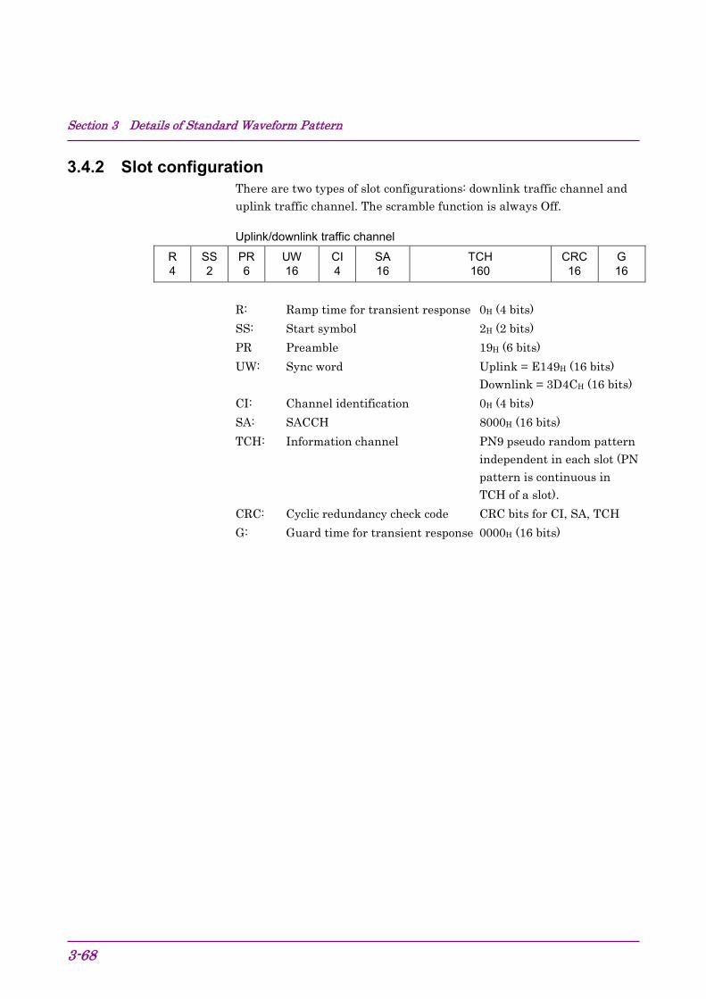
Section 3 Details of Standard Waveform Pattern
3-68
3.4.2 Slot configuration There are two types of slot configurations: downlink traffic channel and uplink traffic channel. The scramble function is always Off.
Uplink/downlink traffic channel
R 4
SS 2
PR 6
UW 16
CI 4
SA 16
TCH 160
CRC 16
G 16
R: Ramp time for transient response 0H (4 bits) SS: Start symbol 2H (2 bits) PR Preamble 19H (6 bits) UW: Sync word Uplink = E149H (16 bits)
Downlink = 3D4CH (16 bits) CI: Channel identification 0H (4 bits) SA: SACCH 8000H (16 bits) TCH: Information channel PN9 pseudo random pattern
independent in each slot (PN pattern is continuous in TCH of a slot).
CRC: Cyclic redundancy check code CRC bits for CI, SA, TCH G: Guard time for transient response 0000H (16 bits)
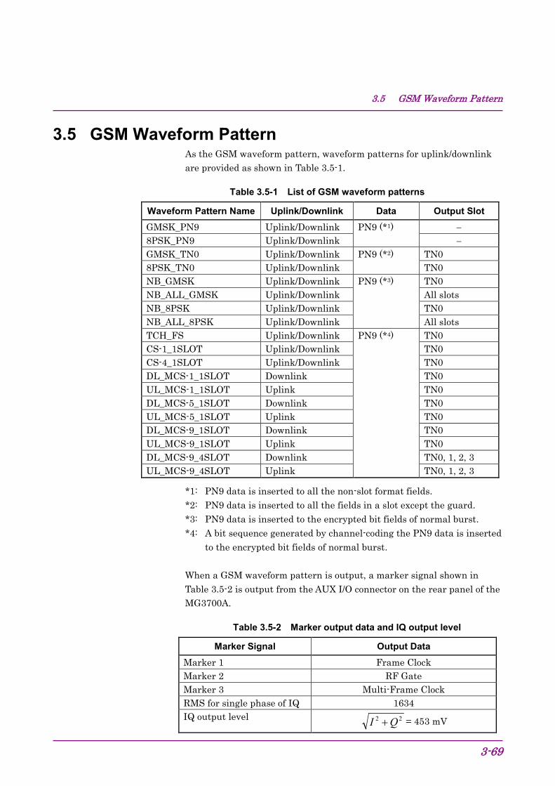
3.5 GSM Waveform Pattern
3-69
3.5 GSM Waveform Pattern As the GSM waveform pattern, waveform patterns for uplink/downlink are provided as shown in Table 3.5-1.
Table 3.5-1 List of GSM waveform patterns
Waveform Pattern Name Uplink/Downlink Data Output Slot GMSK_PN9 Uplink/Downlink PN9 (*1) − 8PSK_PN9 Uplink/Downlink − GMSK_TN0 Uplink/Downlink PN9 (*2) TN0 8PSK_TN0 Uplink/Downlink TN0 NB_GMSK Uplink/Downlink PN9 (*3) TN0 NB_ALL_GMSK Uplink/Downlink All slots NB_8PSK Uplink/Downlink TN0 NB_ALL_8PSK Uplink/Downlink All slots TCH_FS Uplink/Downlink PN9 (*4) TN0 CS-1_1SLOT Uplink/Downlink TN0 CS-4_1SLOT Uplink/Downlink TN0 DL_MCS-1_1SLOT Downlink TN0 UL_MCS-1_1SLOT Uplink TN0 DL_MCS-5_1SLOT Downlink TN0 UL_MCS-5_1SLOT Uplink TN0 DL_MCS-9_1SLOT Downlink TN0 UL_MCS-9_1SLOT Uplink TN0 DL_MCS-9_4SLOT Downlink TN0, 1, 2, 3 UL_MCS-9_4SLOT Uplink TN0, 1, 2, 3
*1: PN9 data is inserted to all the non-slot format fields. *2: PN9 data is inserted to all the fields in a slot except the guard. *3: PN9 data is inserted to the encrypted bit fields of normal burst. *4: A bit sequence generated by channel-coding the PN9 data is inserted
to the encrypted bit fields of normal burst.
When a GSM waveform pattern is output, a marker signal shown in Table 3.5-2 is output from the AUX I/O connector on the rear panel of the MG3700A.
Table 3.5-2 Marker output data and IQ output level
Marker Signal Output Data Marker 1 Frame Clock Marker 2 RF Gate Marker 3 Multi-Frame Clock RMS for single phase of IQ 1634 IQ output level 22 QI + = 453 mV
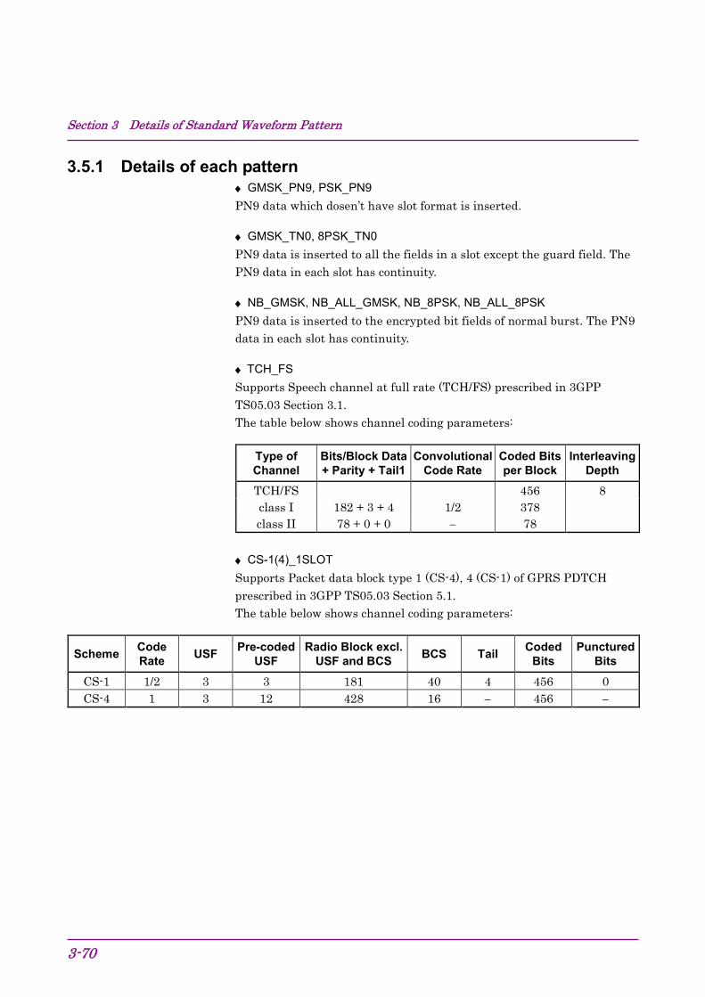
Section 3 Details of Standard Waveform Pattern
3-70
3.5.1 Details of each pattern ♦ GMSK_PN9, PSK_PN9 PN9 data which dosen’t have slot format is inserted.
♦ GMSK_TN0, 8PSK_TN0 PN9 data is inserted to all the fields in a slot except the guard field. The PN9 data in each slot has continuity.
♦ NB_GMSK, NB_ALL_GMSK, NB_8PSK, NB_ALL_8PSK PN9 data is inserted to the encrypted bit fields of normal burst. The PN9 data in each slot has continuity.
♦ TCH_FS Supports Speech channel at full rate (TCH/FS) prescribed in 3GPP TS05.03 Section 3.1. The table below shows channel coding parameters:
Type of Channel
Bits/Block Data + Parity + Tail1
Convolutional Code Rate
Coded Bits per Block
Interleaving Depth
TCH/FS 456 8 class I 182 + 3 + 4 1/2 378 class II 78 + 0 + 0 − 78
♦ CS-1(4)_1SLOT Supports Packet data block type 1 (CS-4), 4 (CS-1) of GPRS PDTCH prescribed in 3GPP TS05.03 Section 5.1. The table below shows channel coding parameters:
Scheme Code Rate USF Pre-coded
USF Radio Block excl.
USF and BCS BCS Tail Coded Bits
Punctured Bits
CS-1 1/2 3 3 181 40 4 456 0 CS-4 1 3 12 428 16 − 456 −
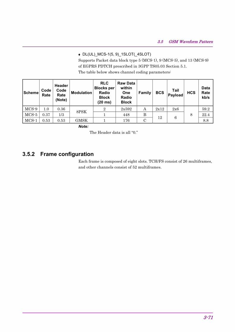
3.5 GSM Waveform Pattern
3-71
♦ DL(UL)_MCS-1(5, 9)_1SLOT(_4SLOT) Supports Packet data block type 5 (MCS-1), 9 (MCS-5), and 13 (MCS-9) of EGPRS PDTCH prescribed in 3GPP TS05.03 Section 5.1. The table below shows channel coding parameters:
Scheme Code Rate
Header Code Rate
(Note)
Modulation
RLC Blocks per
Radio Block
(20 ms)
Raw Data within One
Radio Block
Family BCS Tail Payload HCS
Data Rate kb/s
MCS-9 1.0 0.36 8PSK
2 2x592 A 2x12 2x6 8
59.2 MCS-5 0.37 1/3 1 448 B
12 6 22.4
MCS-1 0.53 0.53 GMSK 1 176 C 8.8 Note:
The Header data is all “0.”
3.5.2 Frame configuration Each frame is composed of eight slots. TCH/FS consist of 26 multiframes, and other channels consist of 52 multiframes.
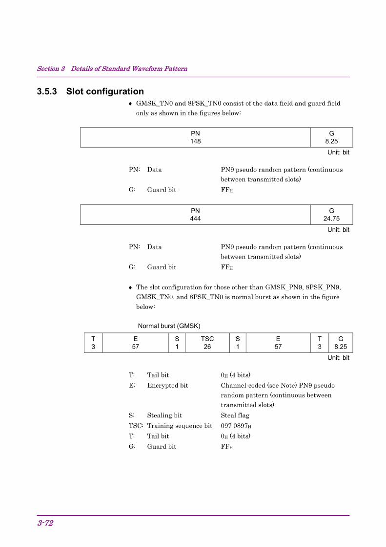
Section 3 Details of Standard Waveform Pattern
3-72
3.5.3 Slot configuration ♦ GMSK_TN0 and 8PSK_TN0 consist of the data field and guard field
only as shown in the figures below:
PN 148
G 8.25
Unit: bit
PN: Data PN9 pseudo random pattern (continuous between transmitted slots)
G: Guard bit FFH
PN 444
G 24.75
Unit: bit
PN: Data PN9 pseudo random pattern (continuous between transmitted slots)
G: Guard bit FFH
♦ The slot configuration for those other than GMSK_PN9, 8PSK_PN9, GMSK_TN0, and 8PSK_TN0 is normal burst as shown in the figure below: Normal burst (GMSK)
T 3
E 57
S 1
TSC 26
S 1
E 57
T 3
G 8.25
Unit: bit
T: Tail bit 0H (4 bits) E: Encrypted bit Channel-coded (see Note) PN9 pseudo
random pattern (continuous between transmitted slots)
S: Stealing bit Steal flag TSC: Training sequence bit 097 0897H T: Tail bit 0H (4 bits) G: Guard bit FFH
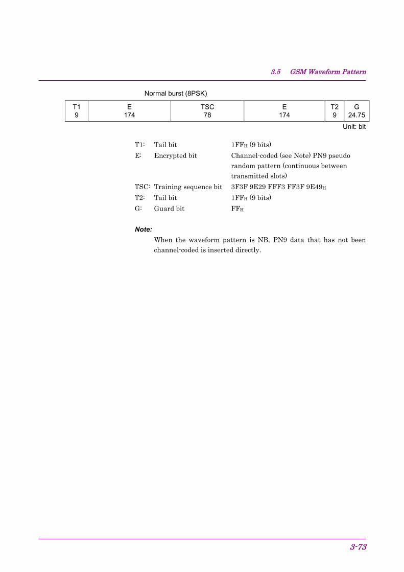
3.5 GSM Waveform Pattern
3-73
Normal burst (8PSK)
T1 9
E 174
TSC 78
E 174
T2 9
G 24.75
Unit: bit
T1: Tail bit 1FFH (9 bits) E: Encrypted bit Channel-coded (see Note) PN9 pseudo
random pattern (continuous between transmitted slots)
TSC: Training sequence bit 3F3F 9E29 FFF3 FF3F 9E49H T2: Tail bit 1FFH (9 bits) G: Guard bit FFH
Note:
When the waveform pattern is NB, PN9 data that has not been channel-coded is inserted directly.
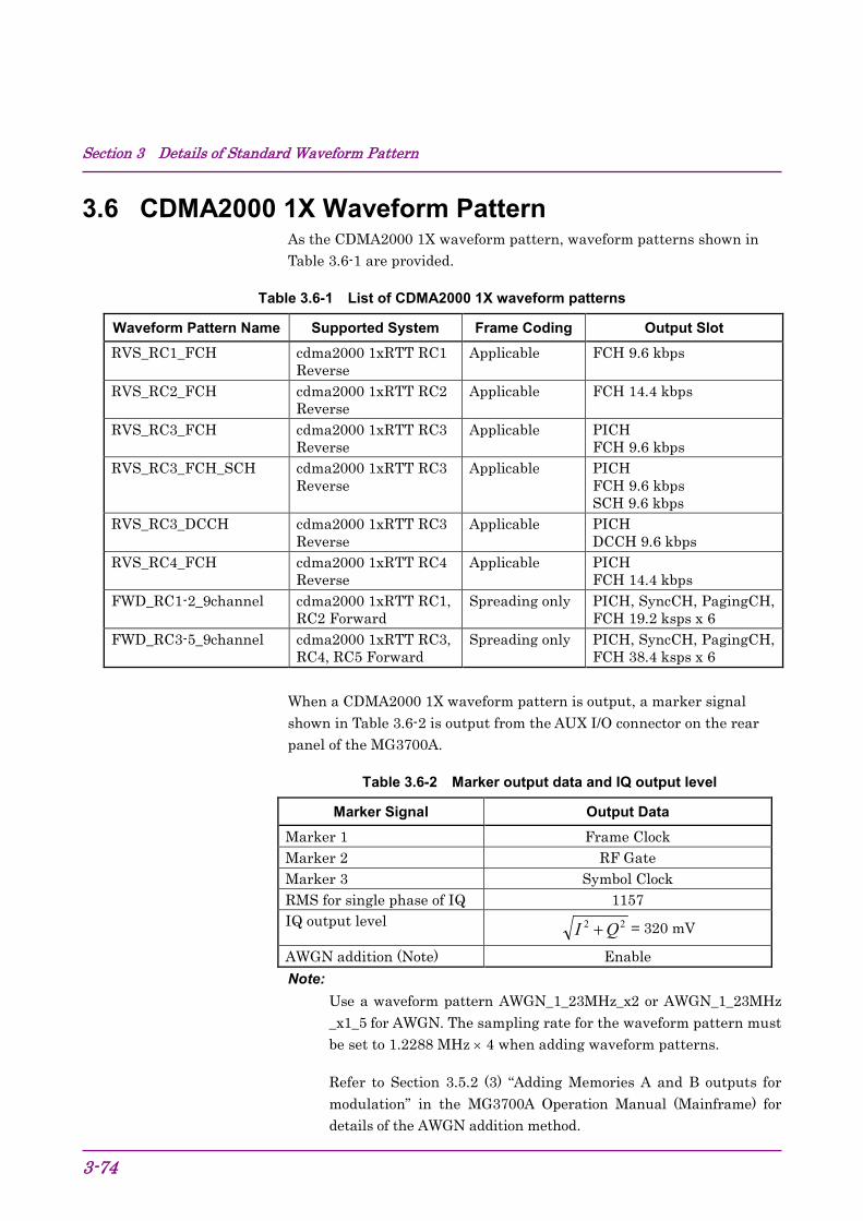
Section 3 Details of Standard Waveform Pattern
3-74
3.6 CDMA2000 1X Waveform Pattern As the CDMA2000 1X waveform pattern, waveform patterns shown in Table 3.6-1 are provided.
Table 3.6-1 List of CDMA2000 1X waveform patterns
Waveform Pattern Name Supported System Frame Coding Output Slot RVS_RC1_FCH cdma2000 1xRTT RC1
Reverse Applicable FCH 9.6 kbps
RVS_RC2_FCH cdma2000 1xRTT RC2 Reverse
Applicable FCH 14.4 kbps
RVS_RC3_FCH cdma2000 1xRTT RC3 Reverse
Applicable PICH FCH 9.6 kbps
RVS_RC3_FCH_SCH cdma2000 1xRTT RC3 Reverse
Applicable PICH FCH 9.6 kbps SCH 9.6 kbps
RVS_RC3_DCCH cdma2000 1xRTT RC3 Reverse
Applicable PICH DCCH 9.6 kbps
RVS_RC4_FCH cdma2000 1xRTT RC4 Reverse
Applicable PICH FCH 14.4 kbps
FWD_RC1-2_9channel cdma2000 1xRTT RC1, RC2 Forward
Spreading only PICH, SyncCH, PagingCH, FCH 19.2 ksps x 6
FWD_RC3-5_9channel cdma2000 1xRTT RC3, RC4, RC5 Forward
Spreading only PICH, SyncCH, PagingCH, FCH 38.4 ksps x 6
When a CDMA2000 1X waveform pattern is output, a marker signal shown in Table 3.6-2 is output from the AUX I/O connector on the rear panel of the MG3700A.
Table 3.6-2 Marker output data and IQ output level
Marker Signal Output Data Marker 1 Frame Clock Marker 2 RF Gate Marker 3 Symbol Clock RMS for single phase of IQ 1157 IQ output level 22 QI + = 320 mV
AWGN addition (Note) Enable Note:
Use a waveform pattern AWGN_1_23MHz_x2 or AWGN_1_23MHz _x1_5 for AWGN. The sampling rate for the waveform pattern must be set to 1.2288 MHz × 4 when adding waveform patterns.
Refer to Section 3.5.2 (3) “Adding Memories A and B outputs for modulation” in the MG3700A Operation Manual (Mainframe) for details of the AWGN addition method.
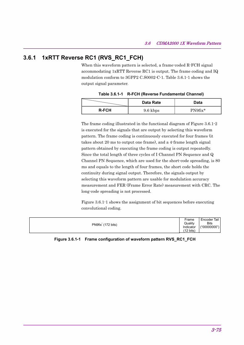
3.6 CDMA2000 1X Waveform Pattern
3-75
3.6.1 1xRTT Reverse RC1 (RVS_RC1_FCH) When this waveform pattern is selected, a frame-coded R-FCH signal accommodating 1xRTT Reverse RC1 is output. The frame coding and IQ modulation conform to 3GPP2 C.S0002-C-1. Table 3.6.1-1 shows the output signal parameter.
Table 3.6.1-1 R-FCH (Reverse Fundamental Channel)
Data Rate Data
R-FCH 9.6 kbps PN9fix*
The frame coding illustrated in the functional diagram of Figure 3.6.1-2 is executed for the signals that are output by selecting this waveform pattern. The frame coding is continuously executed for four frames (it takes about 20 ms to output one frame), and a 4-frame length signal pattern obtained by executing the frame coding is output repeatedly. Since the total length of three cycles of I Channel PN Sequence and Q Channel PN Sequence, which are used for the short-code spreading, is 80 ms and equals to the length of four frames, the short code holds the continuity during signal output. Therefore, the signals output by selecting this waveform pattern are usable for modulation accuracy measurement and FER (Frame Error Rate) measurement with CRC. The long-code spreading is not processed.
Figure 3.6.1-1 shows the assignment of bit sequences before executing convolutional coding.
PN9fix* (172 bits)
Frame Quality
Indicator (12 bits)
Encoder Tail Bits
(“00000000”)
Figure 3.6.1-1 Frame configuration of waveform pattern RVS_RC1_FCH
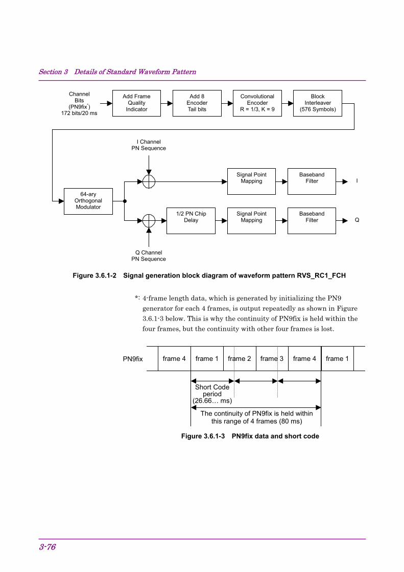
Section 3 Details of Standard Waveform Pattern
3-76
Add Frame Quality
Indicator
Add 8 Encoder Tail bits
Convolutional Encoder
R = 1/3, K = 9
Block Interleaver
(576 Symbols)
64-ary Orthogonal Modulator
1/2 PN Chip Delay
Signal Point Mapping
Baseband Filter
Signal Point Mapping
Baseband Filter
Q Channel PN Sequence
I Channel PN Sequence
172 bits/20 ms
I
Q
Channel Bits
(PN9fix*)
Figure 3.6.1-2 Signal generation block diagram of waveform pattern RVS_RC1_FCH
*: 4-frame length data, which is generated by initializing the PN9 generator for each 4 frames, is output repeatedly as shown in Figure 3.6.1-3 below. This is why the continuity of PN9fix is held within the four frames, but the continuity with other four frames is lost.
Short Code period
(26.66… ms)
frame 4 frame 3 frame 2 frame 1 frame 4 frame 1 PN9fix
The continuity of PN9fix is held within this range of 4 frames (80 ms)
Figure 3.6.1-3 PN9fix data and short code
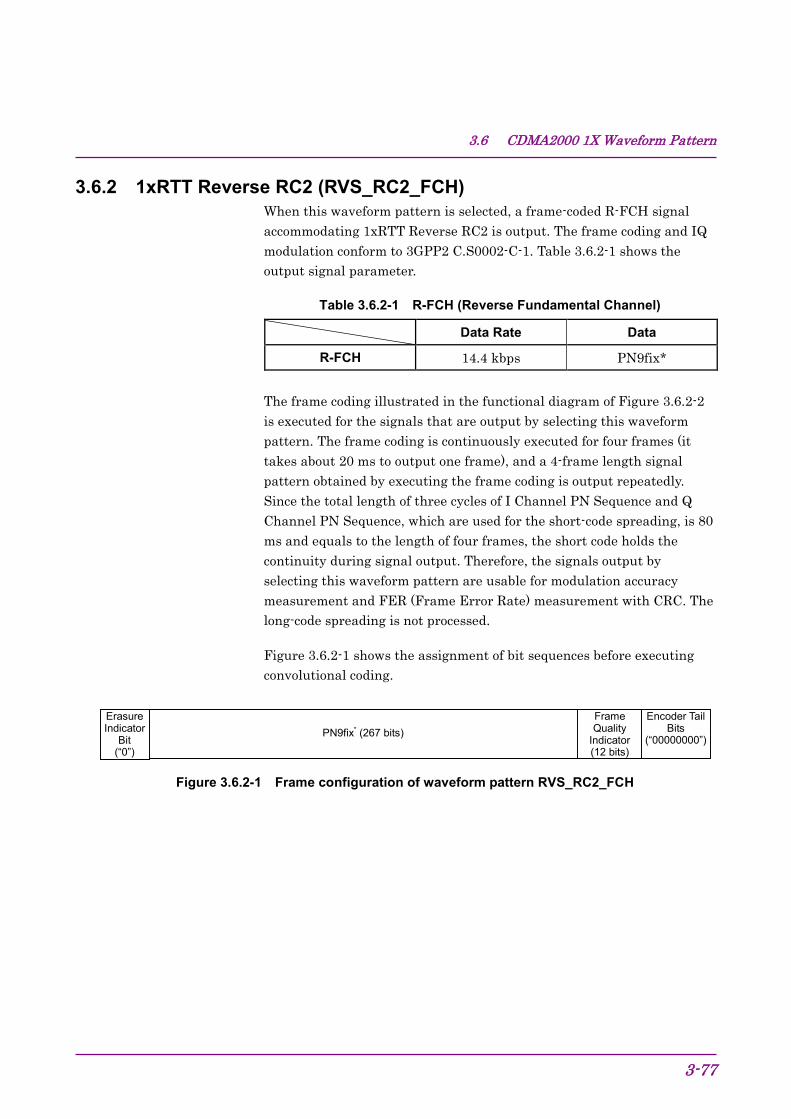
3.6 CDMA2000 1X Waveform Pattern
3-77
3.6.2 1xRTT Reverse RC2 (RVS_RC2_FCH) When this waveform pattern is selected, a frame-coded R-FCH signal accommodating 1xRTT Reverse RC2 is output. The frame coding and IQ modulation conform to 3GPP2 C.S0002-C-1. Table 3.6.2-1 shows the output signal parameter.
Table 3.6.2-1 R-FCH (Reverse Fundamental Channel)
Data Rate Data
R-FCH 14.4 kbps PN9fix*
The frame coding illustrated in the functional diagram of Figure 3.6.2-2 is executed for the signals that are output by selecting this waveform pattern. The frame coding is continuously executed for four frames (it takes about 20 ms to output one frame), and a 4-frame length signal pattern obtained by executing the frame coding is output repeatedly. Since the total length of three cycles of I Channel PN Sequence and Q Channel PN Sequence, which are used for the short-code spreading, is 80 ms and equals to the length of four frames, the short code holds the continuity during signal output. Therefore, the signals output by selecting this waveform pattern are usable for modulation accuracy measurement and FER (Frame Error Rate) measurement with CRC. The long-code spreading is not processed.
Figure 3.6.2-1 shows the assignment of bit sequences before executing convolutional coding.
PN9fix* (267 bits) Frame Quality
Indicator (12 bits)
Encoder Tail Bits
(“00000000”)
Erasure Indicator
Bit (“0”)
Figure 3.6.2-1 Frame configuration of waveform pattern RVS_RC2_FCH
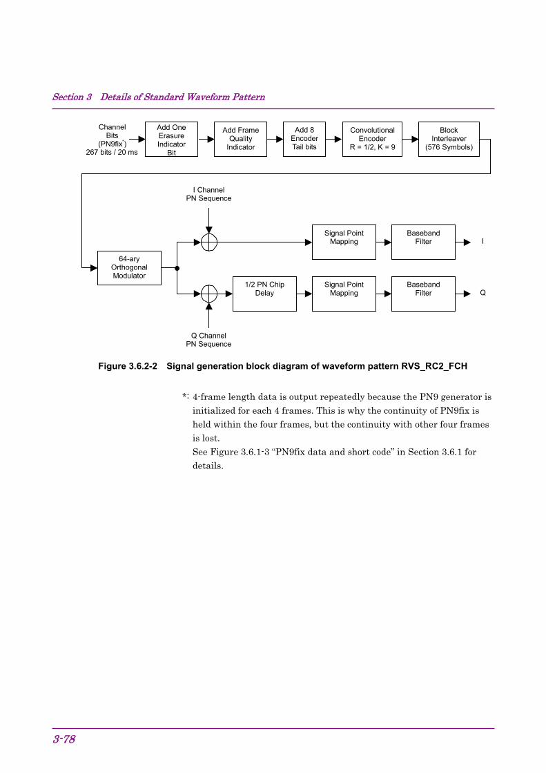
Section 3 Details of Standard Waveform Pattern
3-78
Add Frame Quality
Indicator
Add 8 Encoder Tail bits
Convolutional Encoder
R = 1/2, K = 9
Block Interleaver
(576 Symbols)
64-ary Orthogonal Modulator
1/2 PN Chip Delay
Signal Point Mapping
Baseband Filter
Signal Point Mapping
Baseband Filter
Q Channel PN Sequence
I Channel PN Sequence
267 bits / 20 ms
I
Q
Channel Bits
(PN9fix*)
Add One Erasure Indicator
Bit
Figure 3.6.2-2 Signal generation block diagram of waveform pattern RVS_RC2_FCH
*: 4-frame length data is output repeatedly because the PN9 generator is initialized for each 4 frames. This is why the continuity of PN9fix is held within the four frames, but the continuity with other four frames is lost. See Figure 3.6.1-3 “PN9fix data and short code” in Section 3.6.1 for details.
3.6 CDMA2000 1X Waveform Pattern
3-79
3.6.3 1xRTT Reverse RC3 (1) (RVS_RC3_FCH) When this waveform pattern is selected, a frame-coded multiplexed signal accommodating 1xRTT Reverse RC3 is output. The frame coding and IQ modulation conform to 3GPP2 C.S0002-C-1. The multiplexed channels are R-PICH and R-FCH. Table 3.6.3-1 shows the output signal parameters.
Table 3.6.3-1 R-PICH (Reverse Pilot Channel), R-FCH (Reverse Fundamental Channel)
Walsh Code Code Power Data Rate Data
R-PICH 0 −5.278 dB N/A All “0”
R-FCH 4 −1.528 dB 9.6 kbps PN9fix* The frame coding illustrated in the functional diagrams of Figure 3.6.3-2 and 3.6.3-3 is executed for the signals that are output by selecting this waveform pattern. The frame coding is continuously executed for four frames (it takes about 20 ms to output one frame), and a 4-frame length signal pattern obtained by executing the frame coding is output repeatedly. Since the total length of three cycles of I Channel PN Sequence and Q Channel PN Sequence, which are used for the short-code spreading, is 80 ms and equals to the length of four frames, the short code holds the continuity during signal output. Therefore, the signals output by selecting this waveform pattern are usable for modulation accuracy measurement and FER (Frame Error Rate) measurement with CRC. The long-code spreading is not processed.
Figure 3.6.3-1 shows the assignment of bit sequences before executing convolutional coding.
PN9fix* (172 bits) Frame Quality
Indicator (12 bits)
Encoder Tail Bits
(“00000000”)
Figure 3.6.3-1 Traffic channel frame configuration of waveform pattern RVS_RC3_FCH
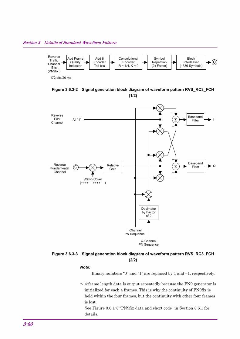
Section 3 Details of Standard Waveform Pattern
3-80
172 bits/20 ms
Add Frame Quality
Indicator
Add 8 Encoder Tail bits
Convolutional Encoder
R = 1/4, K = 9
Symbol Repetition (2x Factor)
Block Interleaver
(1536 Symbols) C
Reverse Traffic
Channel Bits
(PN9fix*)
Figure 3.6.3-2 Signal generation block diagram of waveform pattern RVS_RC3_FCH (1/2)
Decimator by Factor
of 2
Baseband Filter
Baseband Filter
I
Q
I-Channel PN Sequence
Q-Channel PN Sequence
Reverse Pilot
Channel All “1”
Relative Gain
Walsh Cover (++++----++++----)
C Reverse Fundamental
Channel
−
+
Σ
+
+
Σ
Figure 3.6.3-3 Signal generation block diagram of waveform pattern RVS_RC3_FCH (2/2)
Note: Binary numbers “0” and “1” are replaced by 1 and −1, respectively.
*: 4-frame length data is output repeatedly because the PN9 generator is initialized for each 4 frames. This is why the continuity of PN9fix is held within the four frames, but the continuity with other four frames is lost. See Figure 3.6.1-3 “PN9fix data and short code” in Section 3.6.1 for details.
3.6 CDMA2000 1X Waveform Pattern
3-81
3.6.4 1xRTT Reverse RC3 (2) (RVS_RC3_FCH_SCH) When this waveform pattern is selected, a frame-coded multiplexed signal accommodating 1xRTT Reverse RC3 is output. The frame coding and IQ modulation conform to 3GPP2 C.S0002-C-1. The multiplexed channels are R-PICH, R-FCH, and R-SCH. Table 3.6.4-1 shows the output signal parameters.
Table 3.6.4-1 R-PICH (Reverse Pilot Channel), R-FCH (Reverse Fundamental Channel), R-SCH (Reverse Supplemental Channel)
Walsh Code Code Power Data Rate Data
R-PICH 0 −7.5912 dB N/A All “0”
R-FCH 4 −3.8412 dB 9.6 kbps PN9fix*
R-SCH 2 −3.8412 dB 9.6 kbps PN9fix* The frame coding illustrated in the functional diagrams of Figure 3.6.4-2 and 3.6.4-3 is executed for the signals that are output by selecting this waveform pattern. The frame coding is continuously executed for four frames (it takes about 20 ms to output one frame), and a 4-frame length signal pattern obtained by executing the frame coding is output repeatedly. Since the total length of three cycles of I Channel PN Sequence and Q Channel PN Sequence, which are used for the short-code spreading, is 80 ms and equals to the length of four frames, the short code holds the continuity during signal output. Therefore, the signals output by selecting this waveform pattern are usable for modulation accuracy measurement and FER (Frame Error Rate) measurement with CRC. The long-code spreading is not processed.
Figure 3.6.4-1 shows the assignment of bit sequences before executing convolutional coding.
PN9fix* (172 bits) Frame Quality
Indicator (12 bits)
Encoder Tail Bits
(“00000000”)
Figure 3.6.4-1 Traffic channel frame configuration of waveform pattern RVS_RC3_FCH_SCH
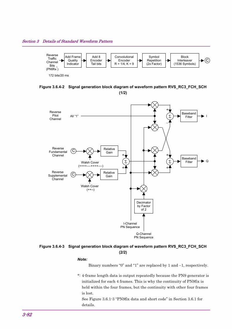
Section 3 Details of Standard Waveform Pattern
3-82
172 bits/20 ms
Add Frame Quality
Indicator
Add 8 Encoder Tail bits
Convolutional Encoder
R = 1/4, K = 9
Symbol Repetition (2x Factor)
Block Interleaver
(1536 Symbols) C
Reverse Traffic
Channel Bits
(PN9fix*)
Figure 3.6.4-2 Signal generation block diagram of waveform pattern RVS_RC3_FCH_SCH (1/2)
Relative Gain
Decimator by Factor
of 2
Baseband Filter
Baseband Filter
I
Q
I-Channel PN Sequence
Q-Channel PN Sequence
Walsh Cover (++++----++++----)
C
Reverse Pilot
Channel
Reverse Fundamental
Channel
All “1”
Relative Gain
Walsh Cover (++--)
C Reverse Supplemental
Channel
+
+
Σ +
+
Σ
−
+
Σ
Figure 3.6.4-3 Signal generation block diagram of waveform pattern RVS_RC3_FCH_SCH (2/2)
Note: Binary numbers “0” and “1” are replaced by 1 and −1, respectively.
*: 4-frame length data is output repeatedly because the PN9 generator is initialized for each 4 frames. This is why the continuity of PN9fix is held within the four frames, but the continuity with other four frames is lost. See Figure 3.6.1-3 “PN9fix data and short code” in Section 3.6.1 for details.
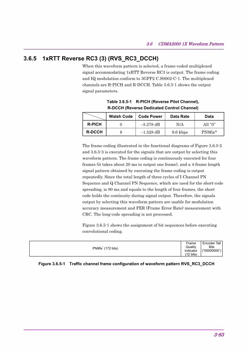
3.6 CDMA2000 1X Waveform Pattern
3-83
3.6.5 1xRTT Reverse RC3 (3) (RVS_RC3_DCCH) When this waveform pattern is selected, a frame-coded multiplexed signal accommodating 1xRTT Reverse RC3 is output. The frame coding and IQ modulation conform to 3GPP2 C.S0002-C-1. The multiplexed channels are R-PICH and R-DCCH. Table 3.6.5-1 shows the output signal parameters.
Table 3.6.5-1 R-PICH (Reverse Pilot Channel), R-DCCH (Reverse Dedicated Control Channel)
Walsh Code Code Power Data Rate Data
R-PICH 0 −5.278 dB N/A All “0”
R-DCCH 8 −1.528 dB 9.6 kbps PN9fix* The frame coding illustrated in the functional diagrams of Figure 3.6.5-2 and 3.6.5-3 is executed for the signals that are output by selecting this waveform pattern. The frame coding is continuously executed for four frames (it takes about 20 ms to output one frame), and a 4-frame length signal pattern obtained by executing the frame coding is output repeatedly. Since the total length of three cycles of I Channel PN Sequence and Q Channel PN Sequence, which are used for the short-code spreading, is 80 ms and equals to the length of four frames, the short code holds the continuity during signal output. Therefore, the signals output by selecting this waveform pattern are usable for modulation accuracy measurement and FER (Frame Error Rate) measurement with CRC. The long-code spreading is not processed.
Figure 3.6.5-1 shows the assignment of bit sequences before executing convolutional coding.
PN9fix* (172 bits) Frame Quality
Indicator (12 bits)
Encoder Tail Bits
(“00000000”)
Figure 3.6.5-1 Traffic channel frame configuration of waveform pattern RVS_RC3_DCCH
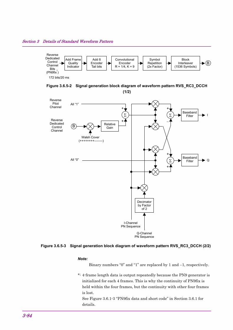
Section 3 Details of Standard Waveform Pattern
3-84
172 bits/20 ms
Add Frame Quality
Indicator
Add 8 Encoder Tail bits
Convolutional Encoder
R = 1/4, K = 9
Symbol Repetition (2x Factor)
Block Interleaver
(1536 Symbols) B
Reverse Dedicated
Control Channel
Bits (PN9fix*)
Figure 3.6.5-2 Signal generation block diagram of waveform pattern RVS_RC3_DCCH (1/2)
Relative Gain
Decimator by Factor
of 2
Baseband Filter
Baseband Filter
I
Q
I-Channel PN Sequence
Q-Channel PN Sequence
Walsh Cover (++++++++--------)
Reverse Pilot
Channel
Reverse Dedicated
Control Channel
B
All “1”
All “0”
+
+
Σ −
+
Σ
+
+
Σ
Figure 3.6.5-3 Signal generation block diagram of waveform pattern RVS_RC3_DCCH (2/2)
Note: Binary numbers “0” and “1” are replaced by 1 and −1, respectively.
*: 4-frame length data is output repeatedly because the PN9 generator is initialized for each 4 frames. This is why the continuity of PN9fix is held within the four frames, but the continuity with other four frames is lost. See Figure 3.6.1-3 “PN9fix data and short code” in Section 3.6.1 for details.
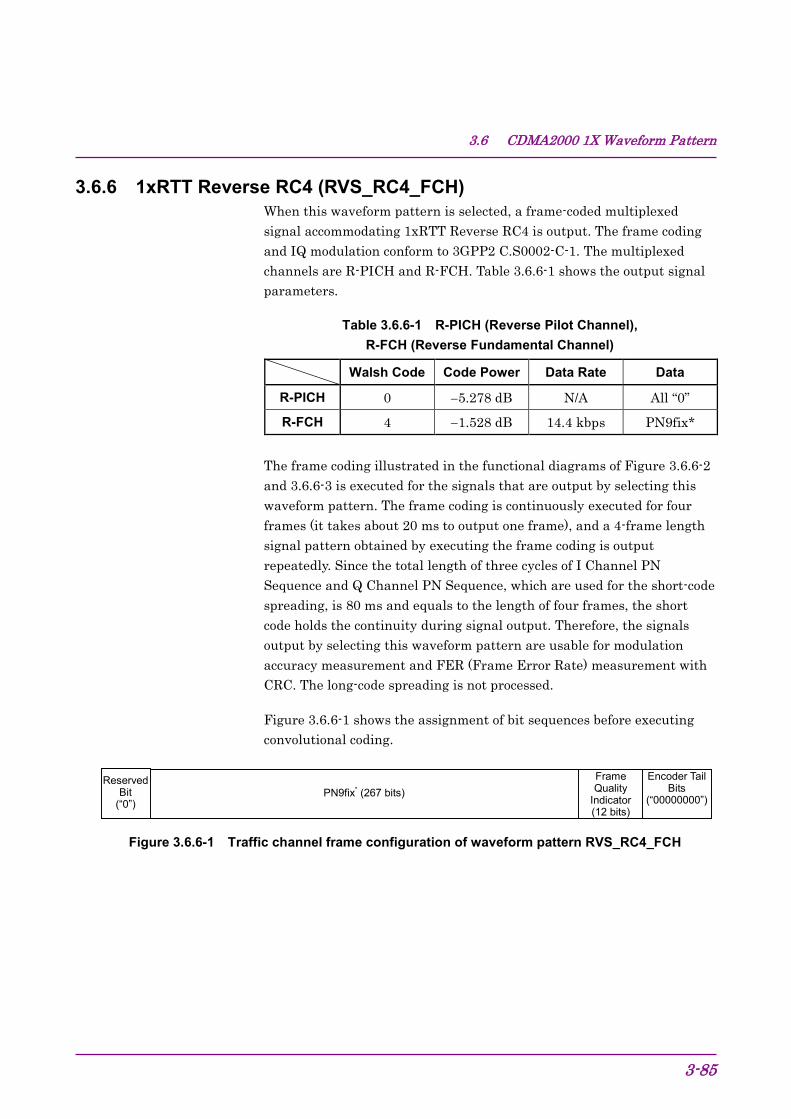
3.6 CDMA2000 1X Waveform Pattern
3-85
3.6.6 1xRTT Reverse RC4 (RVS_RC4_FCH) When this waveform pattern is selected, a frame-coded multiplexed signal accommodating 1xRTT Reverse RC4 is output. The frame coding and IQ modulation conform to 3GPP2 C.S0002-C-1. The multiplexed channels are R-PICH and R-FCH. Table 3.6.6-1 shows the output signal parameters.
Table 3.6.6-1 R-PICH (Reverse Pilot Channel), R-FCH (Reverse Fundamental Channel)
Walsh Code Code Power Data Rate Data
R-PICH 0 −5.278 dB N/A All “0”
R-FCH 4 −1.528 dB 14.4 kbps PN9fix* The frame coding illustrated in the functional diagrams of Figure 3.6.6-2 and 3.6.6-3 is executed for the signals that are output by selecting this waveform pattern. The frame coding is continuously executed for four frames (it takes about 20 ms to output one frame), and a 4-frame length signal pattern obtained by executing the frame coding is output repeatedly. Since the total length of three cycles of I Channel PN Sequence and Q Channel PN Sequence, which are used for the short-code spreading, is 80 ms and equals to the length of four frames, the short code holds the continuity during signal output. Therefore, the signals output by selecting this waveform pattern are usable for modulation accuracy measurement and FER (Frame Error Rate) measurement with CRC. The long-code spreading is not processed.
Figure 3.6.6-1 shows the assignment of bit sequences before executing convolutional coding.
PN9fix* (267 bits) Frame Quality
Indicator (12 bits)
Encoder Tail Bits
(“00000000”)
Reserved Bit
(“0”)
Figure 3.6.6-1 Traffic channel frame configuration of waveform pattern RVS_RC4_FCH
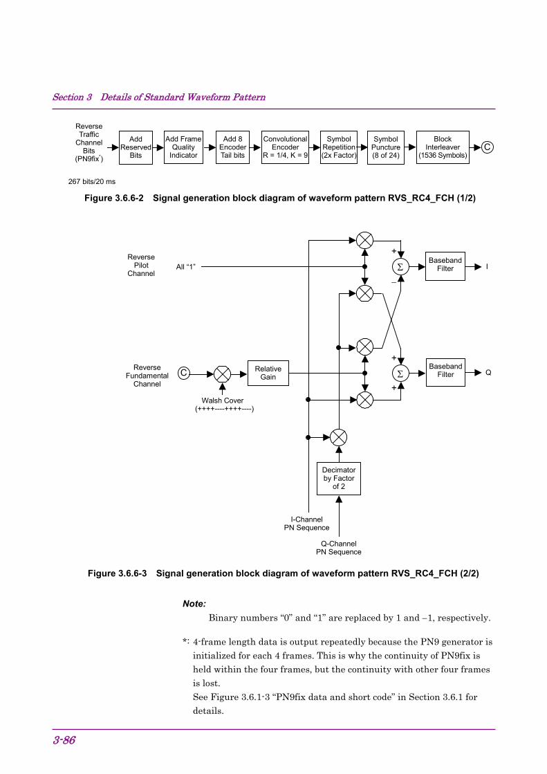
Section 3 Details of Standard Waveform Pattern
3-86
Add Frame
Quality Indicator
Add 8 Encoder Tail bits
Convolutional Encoder
R = 1/4, K = 9
Symbol Repetition (2x Factor)
Block Interleaver
(1536 Symbols) C
Reverse Traffic
Channel Bits
(PN9fix*)
267 bits/20 ms
Add Reserved
Bits
Symbol Puncture (8 of 24)
Figure 3.6.6-2 Signal generation block diagram of waveform pattern RVS_RC4_FCH (1/2)
Relative Gain
Decimator by Factor
of 2
Baseband Filter
Baseband Filter
I
Q
I-Channel PN Sequence
Q-Channel PN Sequence
Walsh Cover (++++----++++----)
C
Reverse Pilot
Channel
Reverse Fundamental
Channel
All “1”
−
+
Σ
+
+
Σ
Figure 3.6.6-3 Signal generation block diagram of waveform pattern RVS_RC4_FCH (2/2)
Note: Binary numbers “0” and “1” are replaced by 1 and −1, respectively.
*: 4-frame length data is output repeatedly because the PN9 generator is initialized for each 4 frames. This is why the continuity of PN9fix is held within the four frames, but the continuity with other four frames is lost. See Figure 3.6.1-3 “PN9fix data and short code” in Section 3.6.1 for details.
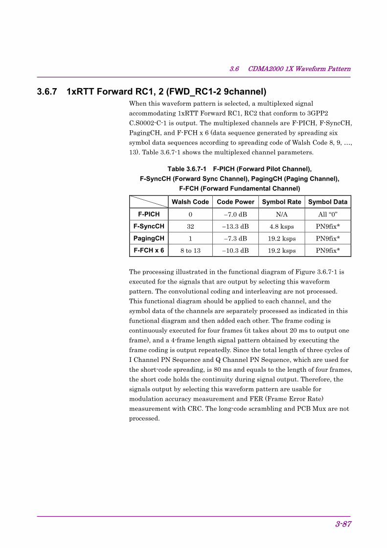
3.6 CDMA2000 1X Waveform Pattern
3-87
3.6.7 1xRTT Forward RC1, 2 (FWD_RC1-2 9channel) When this waveform pattern is selected, a multiplexed signal accommodating 1xRTT Forward RC1, RC2 that conform to 3GPP2 C.S0002-C-1 is output. The multiplexed channels are F-PICH, F-SyncCH, PagingCH, and F-FCH x 6 (data sequence generated by spreading six symbol data sequences according to spreading code of Walsh Code 8, 9, …, 13). Table 3.6.7-1 shows the multiplexed channel parameters.
Table 3.6.7-1 F-PICH (Forward Pilot Channel), F-SyncCH (Forward Sync Channel), PagingCH (Paging Channel),
F-FCH (Forward Fundamental Channel)
Walsh Code Code Power Symbol Rate Symbol Data
F-PICH 0 −7.0 dB N/A All “0”
F-SyncCH 32 −13.3 dB 4.8 ksps PN9fix*
PagingCH 1 −7.3 dB 19.2 ksps PN9fix*
F-FCH x 6 8 to 13 −10.3 dB 19.2 ksps PN9fix* The processing illustrated in the functional diagram of Figure 3.6.7-1 is executed for the signals that are output by selecting this waveform pattern. The convolutional coding and interleaving are not processed. This functional diagram should be applied to each channel, and the symbol data of the channels are separately processed as indicated in this functional diagram and then added each other. The frame coding is continuously executed for four frames (it takes about 20 ms to output one frame), and a 4-frame length signal pattern obtained by executing the frame coding is output repeatedly. Since the total length of three cycles of I Channel PN Sequence and Q Channel PN Sequence, which are used for the short-code spreading, is 80 ms and equals to the length of four frames, the short code holds the continuity during signal output. Therefore, the signals output by selecting this waveform pattern are usable for modulation accuracy measurement and FER (Frame Error Rate) measurement with CRC. The long-code scrambling and PCB Mux are not processed.
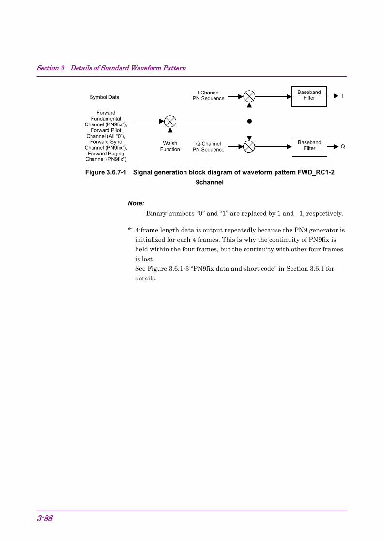
Section 3 Details of Standard Waveform Pattern
3-88
Baseband Filter
Baseband Filter
I
Q
I-Channel PN Sequence
Q-Channel PN Sequence
Walsh Function
Symbol Data
Forward Fundamental
Channel (PN9fix*), Forward Pilot
Channel (All “0”), Forward Sync
Channel (PN9fix*), Forward Paging
Channel (PN9fix*)
Figure 3.6.7-1 Signal generation block diagram of waveform pattern FWD_RC1-2 9channel
Note: Binary numbers “0” and “1” are replaced by 1 and −1, respectively.
*: 4-frame length data is output repeatedly because the PN9 generator is initialized for each 4 frames. This is why the continuity of PN9fix is held within the four frames, but the continuity with other four frames is lost. See Figure 3.6.1-3 “PN9fix data and short code” in Section 3.6.1 for details.
3.6 CDMA2000 1X Waveform Pattern
3-89
3.6.8 1xRTT Forward RC3, 4, 5 (FWD_RC3-5 9channel) When this waveform pattern is selected, a multiplexed signal accommodating 1xRTT Forward RC3, RC4, RC5 that conform to 3GPP2 C.S0002-C-1 is output. The multiplexed channels are F-PICH, F-SyncCH, PagingCH, and F-FCH x 6 (data sequence generated by spreading six symbol data sequences according to spreading code of Walsh Code8, 9, …, 13). Table 3.6.7-1 shows the multiplexed channel parameters.
Table 3.6.8-1 F-PICH (Forward Pilot Channel), F-SyncCH (Forward Sync Channel), PagingCH (Paging Channel),
F-FCH (Forward Fundamental Channel)
Walsh Code Code Power Symbol Rate Symbol Data
F-PICH 0 −7.0 dB N/A All “0”
F-SyncCH 32 −13.3 dB 4.8 ksps PN9fix*
PagingCH 1 −7.3 dB 19.2 ksps PN9fix*
F-FCH x 6 8 to 13 −10.3 dB 38.4 ksps PN9fix* The processing illustrated in the functional diagrams of Figs. 3.6.8-1 and 3.6.8-2 is executed for the signals that are output by selecting this waveform pattern. The convolutional coding and interleaving are not processed. This functional diagram should be applied to each channel, and the symbol data of the channels are separately processed as indicated in this functional diagram and then added each other. The frame coding is continuously executed for four frames (it takes about 20 ms to output one frame), and a 4-frame length signal pattern obtained by executing the frame coding is output repeatedly. Since the total length of three cycles of I Channel PN Sequence and Q Channel PN Sequence, which are used for the short-code spreading, is 80 ms and equals to the length of four frames, the short code holds the continuity during signal output. Therefore, the signals output by selecting this waveform pattern are usable for modulation accuracy measurement and FER (Frame Error Rate) measurement with CRC. The long-code scrambling and PCB Mux are not processed.
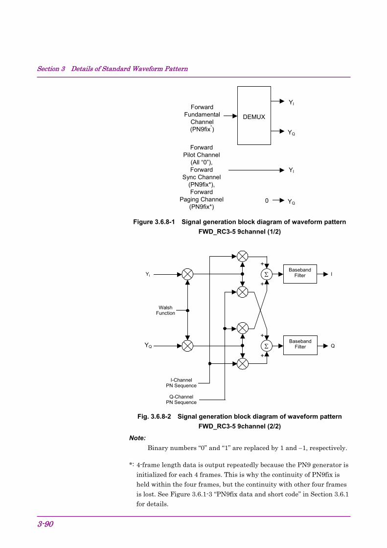
Section 3 Details of Standard Waveform Pattern
3-90
0
YQ
YI
Forward Pilot Channel
(All “0”), Forward
Sync Channel (PN9fix*), Forward
Paging Channel (PN9fix*)
DEMUX
YQ
YI Forward
Fundamental Channel (PN9fix*)
Figure 3.6.8-1 Signal generation block diagram of waveform pattern FWD_RC3-5 9channel (1/2)
Baseband Filter
Baseband Filter
I
Q
I-Channel PN Sequence
Q-Channel PN Sequence
Walsh Function
YI
YQ
+
+
Σ
+
+
Σ
Fig. 3.6.8-2 Signal generation block diagram of waveform pattern FWD_RC3-5 9channel (2/2)
Note: Binary numbers “0” and “1” are replaced by 1 and −1, respectively.
*: 4-frame length data is output repeatedly because the PN9 generator is initialized for each 4 frames. This is why the continuity of PN9fix is held within the four frames, but the continuity with other four frames is lost. See Figure 3.6.1-3 “PN9fix data and short code” in Section 3.6.1 for details.
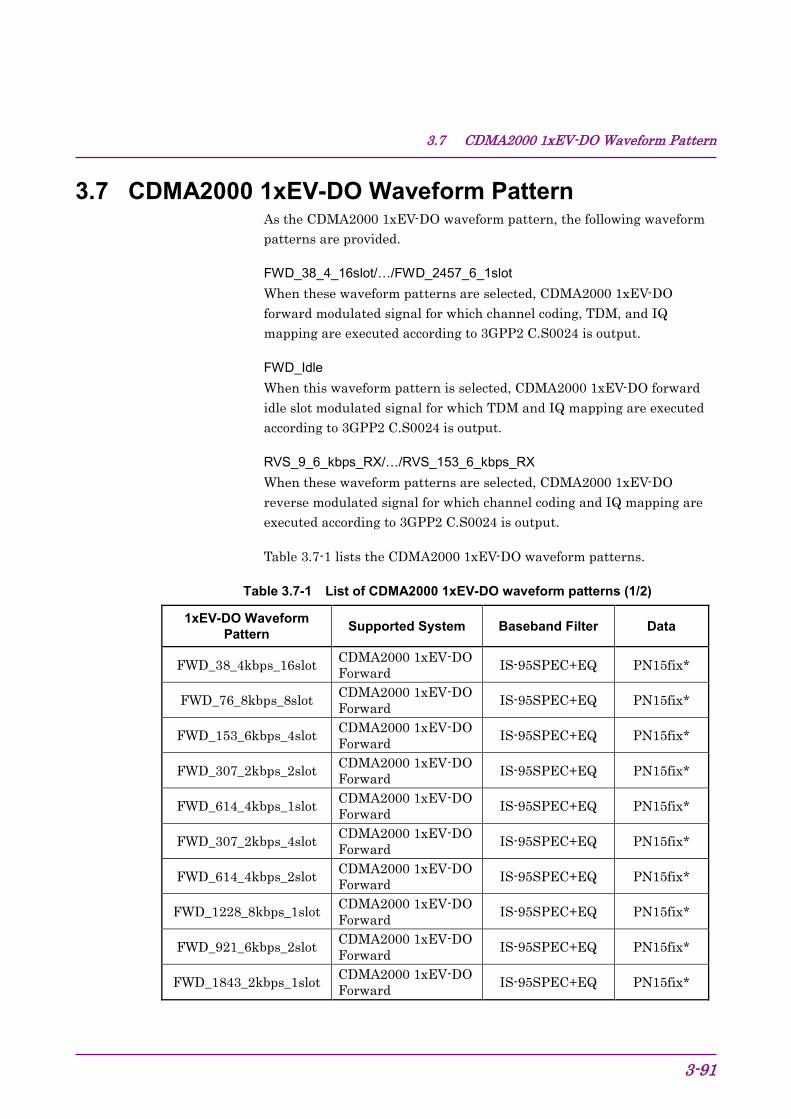
3.7 CDMA2000 1xEV-DO Waveform Pattern
3-91
3.7 CDMA2000 1xEV-DO Waveform Pattern As the CDMA2000 1xEV-DO waveform pattern, the following waveform patterns are provided.
FWD_38_4_16slot/…/FWD_2457_6_1slot When these waveform patterns are selected, CDMA2000 1xEV-DO forward modulated signal for which channel coding, TDM, and IQ mapping are executed according to 3GPP2 C.S0024 is output.
FWD_Idle When this waveform pattern is selected, CDMA2000 1xEV-DO forward idle slot modulated signal for which TDM and IQ mapping are executed according to 3GPP2 C.S0024 is output.
RVS_9_6_kbps_RX/…/RVS_153_6_kbps_RX When these waveform patterns are selected, CDMA2000 1xEV-DO reverse modulated signal for which channel coding and IQ mapping are executed according to 3GPP2 C.S0024 is output.
Table 3.7-1 lists the CDMA2000 1xEV-DO waveform patterns.
Table 3.7-1 List of CDMA2000 1xEV-DO waveform patterns (1/2)
1xEV-DO Waveform Pattern Supported System Baseband Filter Data
FWD_38_4kbps_16slot CDMA2000 1xEV-DO Forward IS-95SPEC+EQ PN15fix*
FWD_76_8kbps_8slot CDMA2000 1xEV-DO Forward IS-95SPEC+EQ PN15fix*
FWD_153_6kbps_4slot CDMA2000 1xEV-DO Forward IS-95SPEC+EQ PN15fix*
FWD_307_2kbps_2slot CDMA2000 1xEV-DO Forward IS-95SPEC+EQ PN15fix*
FWD_614_4kbps_1slot CDMA2000 1xEV-DO Forward IS-95SPEC+EQ PN15fix*
FWD_307_2kbps_4slot CDMA2000 1xEV-DO Forward IS-95SPEC+EQ PN15fix*
FWD_614_4kbps_2slot CDMA2000 1xEV-DO Forward IS-95SPEC+EQ PN15fix*
FWD_1228_8kbps_1slot CDMA2000 1xEV-DO Forward IS-95SPEC+EQ PN15fix*
FWD_921_6kbps_2slot CDMA2000 1xEV-DO Forward IS-95SPEC+EQ PN15fix*
FWD_1843_2kbps_1slot CDMA2000 1xEV-DO Forward IS-95SPEC+EQ PN15fix*
Section 3 Details of Standard Waveform Pattern
3-92
Table 3.7-1 List of CDMA2000 1xEV-DO waveform patterns (2/2)
1xEV-DO Waveform Pattern Supported System Baseband Filter Data
FWD_1228_8kbps_2slot CDMA2000 1xEV-DO Forward IS-95SPEC+EQ PN15fix*
FWD_2457_6kbps_1slot CDMA2000 1xEV-DO Forward IS-95SPEC+EQ PN15fix*
FWD_Idle CDMA2000 1xEV-DO Forward IS-95SPEC+EQ −
RVS_9_6kbps_RX CDMA2000 1xEV-DO Reverse IS-95SPEC PN9fix*
RVS_19_2kbps_RX CDMA2000 1xEV-DO Reverse IS-95SPEC PN9fix*
RVS_38_4kbps_RX CDMA2000 1xEV-DO Reverse IS-95SPEC PN9fix*
RVS_76_8kbps_RX CDMA2000 1xEV-DO Reverse IS-95SPEC PN9fix*
RVS_153_6kbps_RX CDMA2000 1xEV-DO Reverse IS-95SPEC PN9fix*
RVS_9_6kbps_TX CDMA2000 1xEV-DO Reverse IS-95SPEC PN9fix*
RVS_19_2kbps_TX CDMA2000 1xEV-DO Reverse IS-95SPEC PN9fix*
RVS_38_4kbps_TX CDMA2000 1xEV-DO Reverse IS-95SPEC PN9fix*
RVS_76_8kbps_TX CDMA2000 1xEV-DO Reverse IS-95SPEC PN9fix*
RVS_153_6kbps_TX CDMA2000 1xEV-DO Reverse IS-95SPEC PN9fix*
*: Indicates the PN sequence that was extracted for each packet. Therefore, the PN sequence is not continuous between the last data of a packet and the first data of the next packet.
When a CDMA2000 1xEV-DO waveform pattern is output, a marker signal shown in Table 3.7-2 is output from the AUX I/O connector on the rear panel of the MG3700A.
3.7 CDMA2000 1xEV-DO Waveform Pattern
3-93
Table 3.7-2 Marker output data and IQ output level
Marker Signal Output Data Marker 1 Frame Clock Marker 2 RF Gate Marker 3 Symbol Clock RMS for single phase of IQ 1157 IQ output level 22 QI + = 320 mV
AWGN addition (Note) Enable Note:
Use a waveform pattern AWGN_1_23MHz_x2 or AWGN_1_23MHz _x1_5 for AWGN. The sampling rate for the waveform pattern must be set to 1.2288 MHz × 4 when adding waveform patterns.
Refer to Section 3.5.2 (3) “Adding Memories A and B outputs for modulation” in the MG3700A Operation Manual (Mainframe) for details of the AWGN addition method.
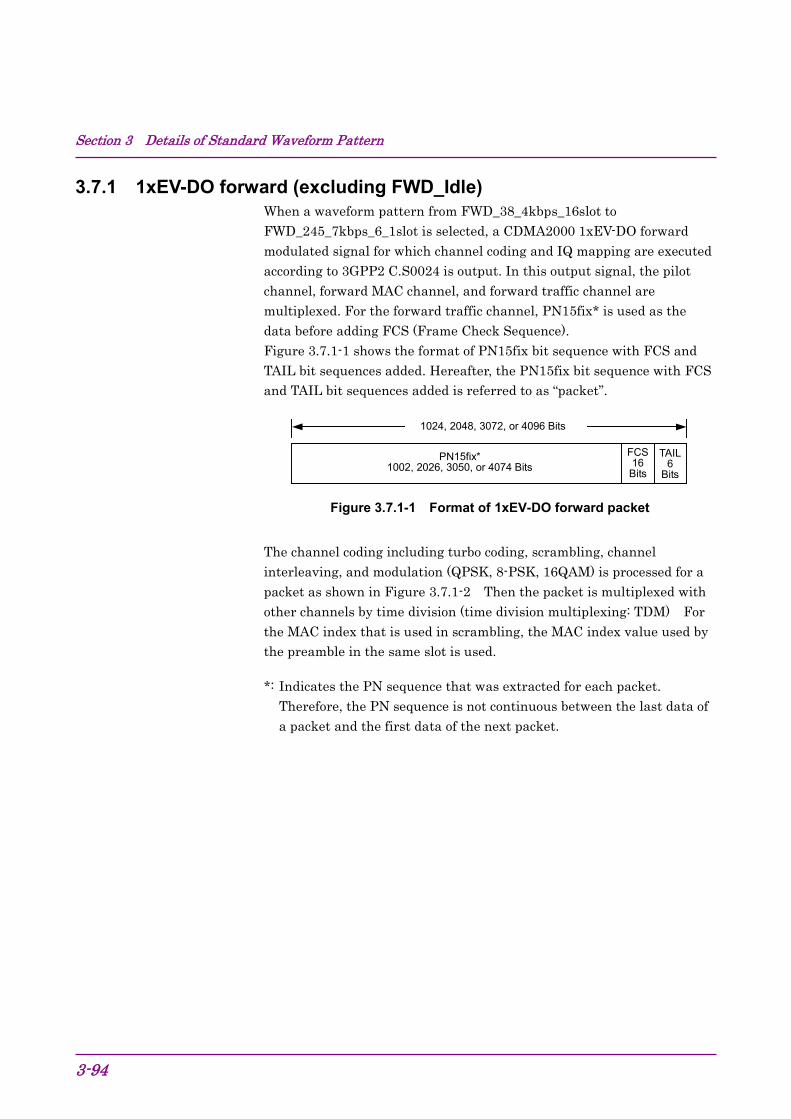
Section 3 Details of Standard Waveform Pattern
3-94
3.7.1 1xEV-DO forward (excluding FWD_Idle) When a waveform pattern from FWD_38_4kbps_16slot to FWD_245_7kbps_6_1slot is selected, a CDMA2000 1xEV-DO forward modulated signal for which channel coding and IQ mapping are executed according to 3GPP2 C.S0024 is output. In this output signal, the pilot channel, forward MAC channel, and forward traffic channel are multiplexed. For the forward traffic channel, PN15fix* is used as the data before adding FCS (Frame Check Sequence). Figure 3.7.1-1 shows the format of PN15fix bit sequence with FCS and TAIL bit sequences added. Hereafter, the PN15fix bit sequence with FCS and TAIL bit sequences added is referred to as “packet”.
FCS16Bits
TAIL6
Bits
PN15fix*1002, 2026, 3050, or 4074 Bits
1024, 2048, 3072, or 4096 Bits
Figure 3.7.1-1 Format of 1xEV-DO forward packet
The channel coding including turbo coding, scrambling, channel interleaving, and modulation (QPSK, 8-PSK, 16QAM) is processed for a packet as shown in Figure 3.7.1-2 Then the packet is multiplexed with other channels by time division (time division multiplexing: TDM) For the MAC index that is used in scrambling, the MAC index value used by the preamble in the same slot is used.
*: Indicates the PN sequence that was extracted for each packet. Therefore, the PN sequence is not continuous between the last data of a packet and the first data of the next packet.
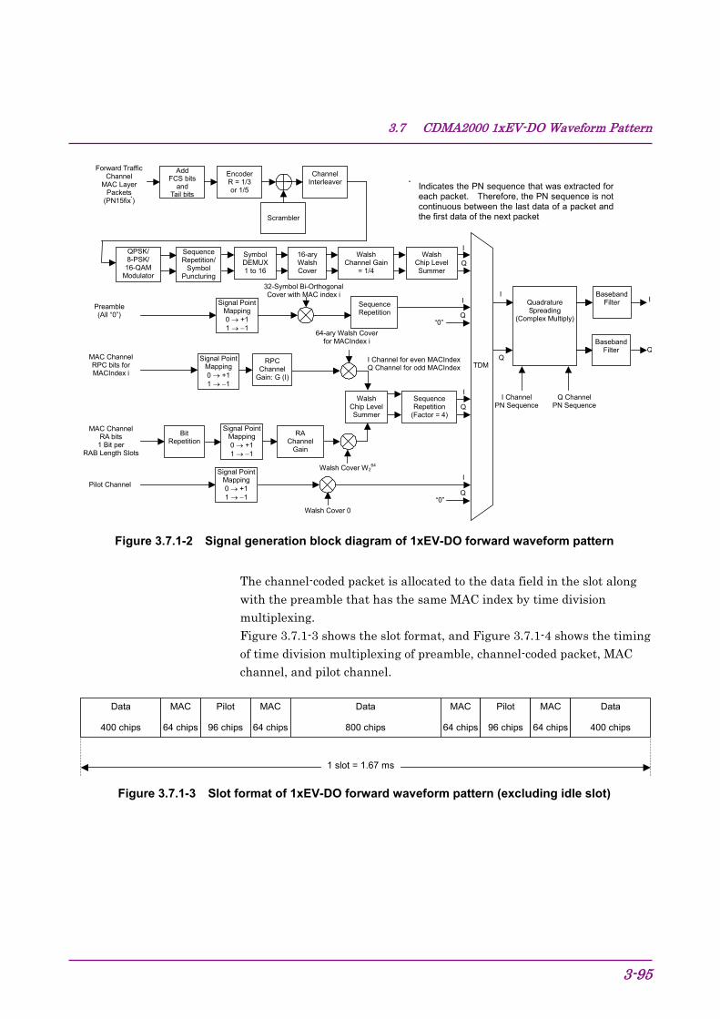
3.7 CDMA2000 1xEV-DO Waveform Pattern
3-95
Walsh Cover 0
I
Q
Walsh Cover W264
Signal Point Mapping 0 → +1 1 → −1
32-Symbol Bi-Orthogonal Cover with MAC index i
Preamble (All “0”)
Sequence Repetition
“0”
Pilot Channel
“0”
64-ary Walsh Cover for MACIndex i
RA Channel
Gain
Sequence Repetition/
Symbol Puncturing
Symbol DEMUX 1 to 16
16-ary Walsh Cover
Walsh Channel Gain
= 1/4
Forward Traffic Channel
MAC Layer Packets
(PN15fix*)
Walsh Chip Level Summer
MAC Channel RPC bits for MACIndex i
MAC Channel RA bits
1 Bit per RAB Length Slots
I Channel PN Sequence
Q Channel PN Sequence
Quadrature Spreading
(Complex Multiply)
I
Q
Q
I
Q
I
Q
I
I Channel for even MACIndex Q Channel for odd MACIndex
Encoder R = 1/3 or 1/5
QPSK/ 8-PSK/ 16-QAM
Modulator
Channel Interleaver
Scrambler
Add FCS bits
and Tail bits
Sequence Repetition
(Factor = 4)
TDM
Signal Point Mapping 0 → +1 1 → −1
Signal Point Mapping 0 → +1 1 → −1
Signal Point
Mapping 0 → +1 1 → −1
Walsh Chip Level Summer
Bit Repetition
* Indicates the PN sequence that was extracted for each packet. Therefore, the PN sequence is not continuous between the last data of a packet and the first data of the next packet
RPC Channel
Gain: G (I)
Baseband Filter
Baseband Filter
I
Q
Figure 3.7.1-2 Signal generation block diagram of 1xEV-DO forward waveform pattern
The channel-coded packet is allocated to the data field in the slot along with the preamble that has the same MAC index by time division multiplexing. Figure 3.7.1-3 shows the slot format, and Figure 3.7.1-4 shows the timing of time division multiplexing of preamble, channel-coded packet, MAC channel, and pilot channel.
MAC
64 chips
Pilot
96 chips
MAC
64 chips
Data
800 chips
MAC
64 chips
Pilot
96 chips
MAC
64 chips
Data
400 chips
1 slot = 1.67 ms
Data
400 chips
Figure 3.7.1-3 Slot format of 1xEV-DO forward waveform pattern (excluding idle slot)
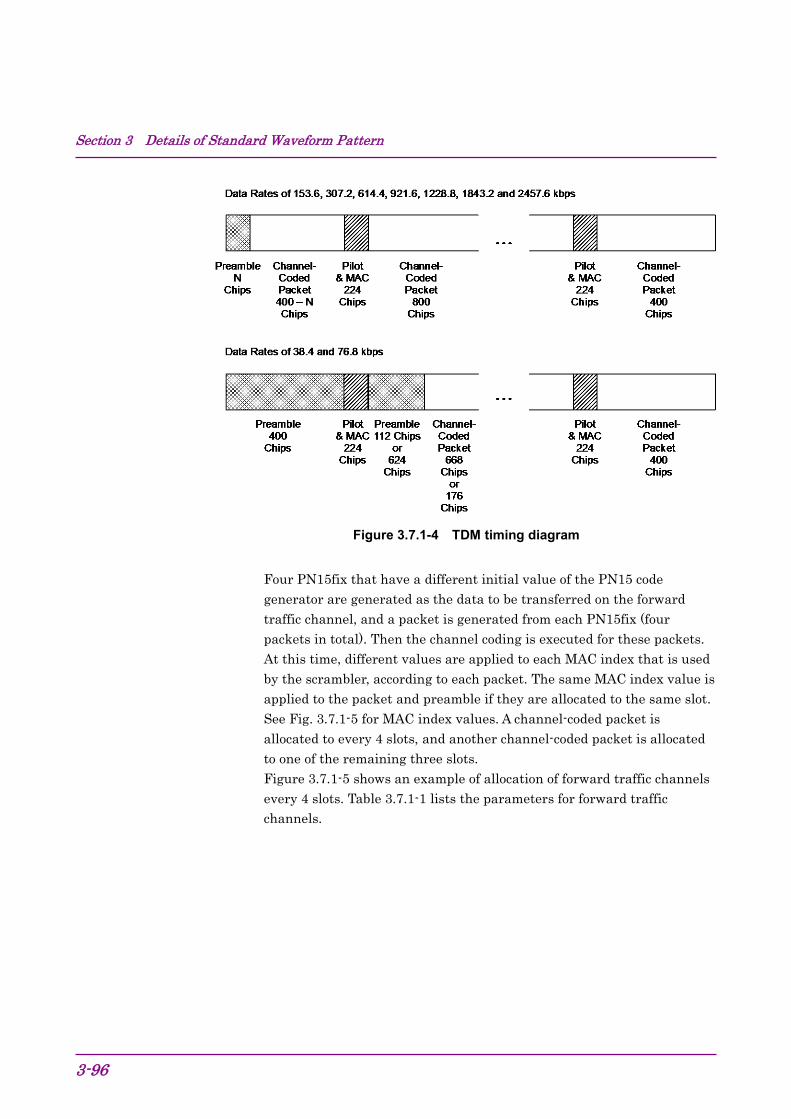
Section 3 Details of Standard Waveform Pattern
3-96
Figure 3.7.1-4 TDM timing diagram
Four PN15fix that have a different initial value of the PN15 code generator are generated as the data to be transferred on the forward traffic channel, and a packet is generated from each PN15fix (four packets in total). Then the channel coding is executed for these packets. At this time, different values are applied to each MAC index that is used by the scrambler, according to each packet. The same MAC index value is applied to the packet and preamble if they are allocated to the same slot. See Fig. 3.7.1-5 for MAC index values. A channel-coded packet is allocated to every 4 slots, and another channel-coded packet is allocated to one of the remaining three slots. Figure 3.7.1-5 shows an example of allocation of forward traffic channels every 4 slots. Table 3.7.1-1 lists the parameters for forward traffic channels.
3.7 CDMA2000 1xEV-DO Waveform Pattern
3-97
Table 3.7.1-1 List of traffic channel parameters
1xEV-DO Modulated Signal
Data Rate (kbps) Slot Packet
(Bit) Preamble
(Chip) Modulation
Type FWD_38_4kbps_16slot 38.4 16 1024 1024 QPSK FWD_76_8kbps_8slot 76.8 8 1024 512 QPSK FWD_153_6kbps_4slot 153.6 4 1024 256 QPSK FWD_307_2kbps_2slot 307.2 2 1024 128 QPSK FWD_614_4kbps_1slot 614.4 1 1024 64 QPSK FWD_307_2kbps_4slot 307.2 4 2048 128 QPSK FWD_614_4kbps_2slot 614.4 2 2048 64 QPSK FWD_1228_8kbps_1slot 1228.8 1 2048 64 QPSK FWD_921_6kbps_2slot 921.6 2 3072 64 8-PSK FWD_1843_2kbps_1slot 1843.2 1 3072 64 8-PSK FWD_1228_8kbps_2slot 1228.8 2 4096 64 16QAM FWD_2457_6kbps_1slot 2457.6 1 4096 64 16QAM
Table 3.7.1-2 lists the parameter for the MAC channel:
Table 3.7.1-2 List of MAC channel parameter
MAC Index RABit RPCBit
4 (RA Channel), 5-17 (RPC Channel) Random Random
The RPCBit to be transferred on the RPC channel and the RABit to be transferred on the RA channel of the MAC channel are set at random. There are 13 RPC channels and one RA channel. These MAC channels are spread by the Walsh cover, which is determined depending on the MAC index, and then multiplexed. The MAC channels are allocated to the MAC field in a slot as shown in Figure 3.7.1-3. Figure 3.7.1-5 shows the relationship between the slot and the data transmitted by the MAC channel and traffic channel.
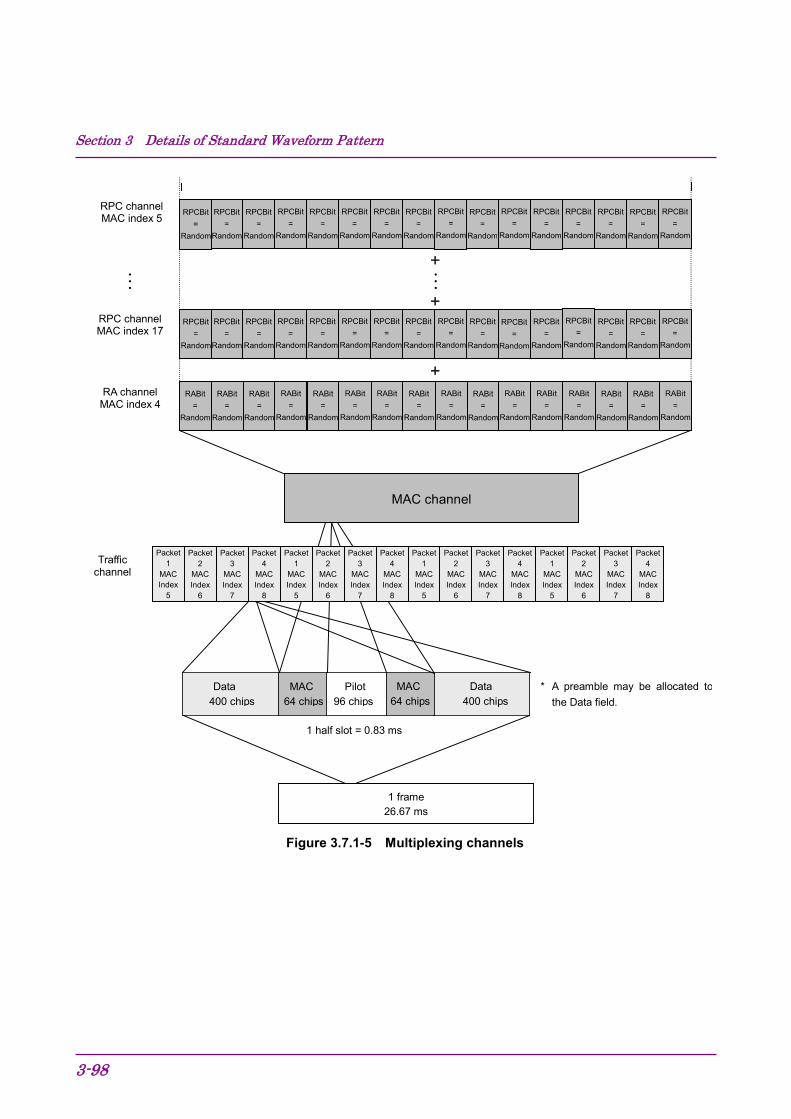
Section 3 Details of Standard Waveform Pattern
3-98
RPC channel MAC index 5
RPCBit =
Random
RPCBit =
Random
RPCBit =
Random
RPCBit =
Random RPCBit
= Random
RPCBit =
Random RPCBit
= Random
RPCBit =
Random
RPCBit =
Random
RPCBit =
Random
RPCBit =
Random
RPCBit =
Random RPCBit
= Random
RPCBit =
Random
RPC channel MAC index 17
RPCBit =
Random
RPCBit =
Random
RPCBit =
Random
RPCBit =
Random
RPCBit =
Random
RA channel MAC index 4
1 frame 26.67 ms
1 half slot = 0.83 ms
MAC 64 chips
Pilot 96 chips
MAC 64 chips
Data 400 chips
Data 400 chips
Traffic channel
Packet 1
MAC Index
5
Packet 3
MAC Index
7
Packet 2
MAC Index
6
Packet 4
MAC Index
8
Packet 1
MAC Index
5
Packet 3
MAC Index
7
Packet 2
MAC Index
6
Packet 4
MAC Index
8
Packet 1
MAC Index
5
Packet 3
MAC Index
7
Packet 2
MAC Index
6
Packet 4
MAC Index
8
Packet 1
MAC Index
5
Packet 3
MAC Index
7
Packet 2
MAC Index
6
Packet 4
MAC Index
8
RPCBit =
Random
RPCBit =
Random RPCBit
= Random
RPCBit =
Random
RPCBit =
Random
RPCBit =
Random
RPCBit =
Random
RPCBit =
Random
RPCBit =
Random
RPCBit =
Random
RPCBit =
Random
MAC channel
RABit =
Random
RABit =
Random
RABit =
Random
RABit =
Random
RABit =
Random
RABit =
Random
RABit =
Random
RABit =
Random
RABit =
Random
RABit =
Random
RABit =
Random
RABit =
Random
RABit =
Random
RABit =
Random
RABit =
Random
RABit =
Random
RPCBit =
Random
RPCBit =
Random
. . . +
+
. . .
+
* A preamble may be allocated to the Data field.
Figure 3.7.1-5 Multiplexing channels
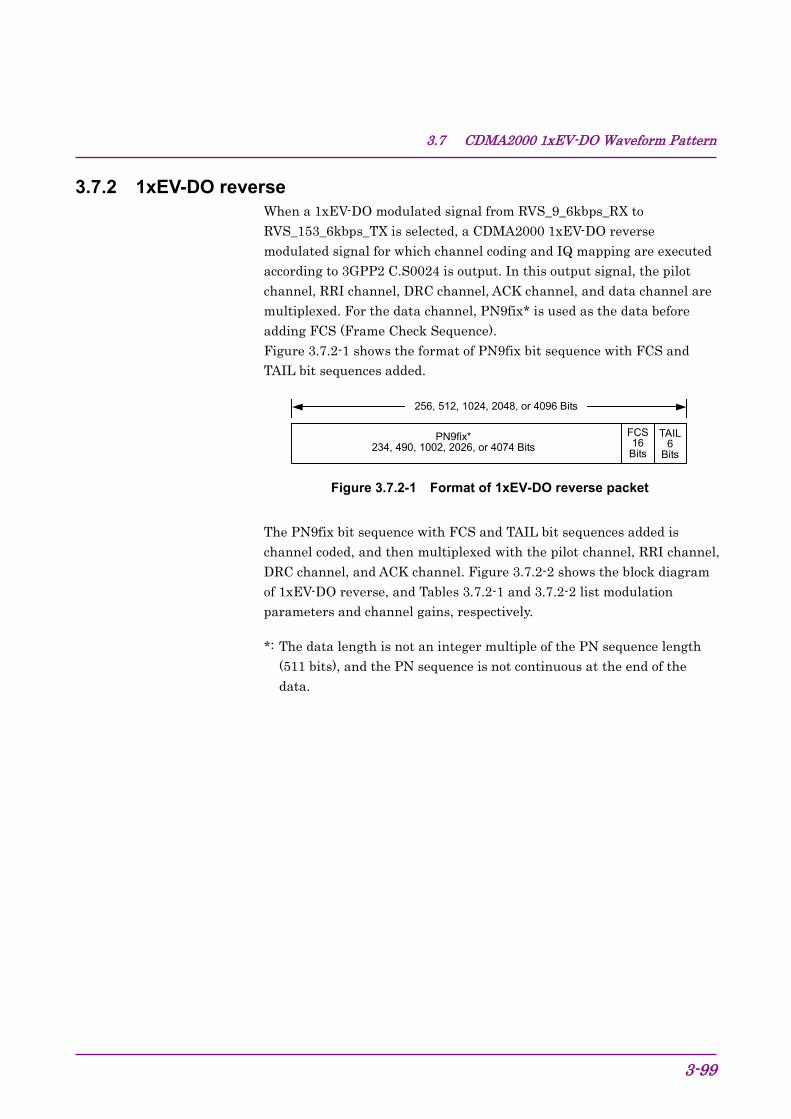
3.7 CDMA2000 1xEV-DO Waveform Pattern
3-99
3.7.2 1xEV-DO reverse When a 1xEV-DO modulated signal from RVS_9_6kbps_RX to RVS_153_6kbps_TX is selected, a CDMA2000 1xEV-DO reverse modulated signal for which channel coding and IQ mapping are executed according to 3GPP2 C.S0024 is output. In this output signal, the pilot channel, RRI channel, DRC channel, ACK channel, and data channel are multiplexed. For the data channel, PN9fix* is used as the data before adding FCS (Frame Check Sequence). Figure 3.7.2-1 shows the format of PN9fix bit sequence with FCS and TAIL bit sequences added.
FCS 16 Bits
TAIL
6 Bits
PN9fix* 234, 490, 1002, 2026, or 4074 Bits
256, 512, 1024, 2048, or 4096 Bits
Figure 3.7.2-1 Format of 1xEV-DO reverse packet
The PN9fix bit sequence with FCS and TAIL bit sequences added is channel coded, and then multiplexed with the pilot channel, RRI channel, DRC channel, and ACK channel. Figure 3.7.2-2 shows the block diagram of 1xEV-DO reverse, and Tables 3.7.2-1 and 3.7.2-2 list modulation parameters and channel gains, respectively.
*: The data length is not an integer multiple of the PN sequence length (511 bits), and the PN sequence is not continuous at the end of the data.
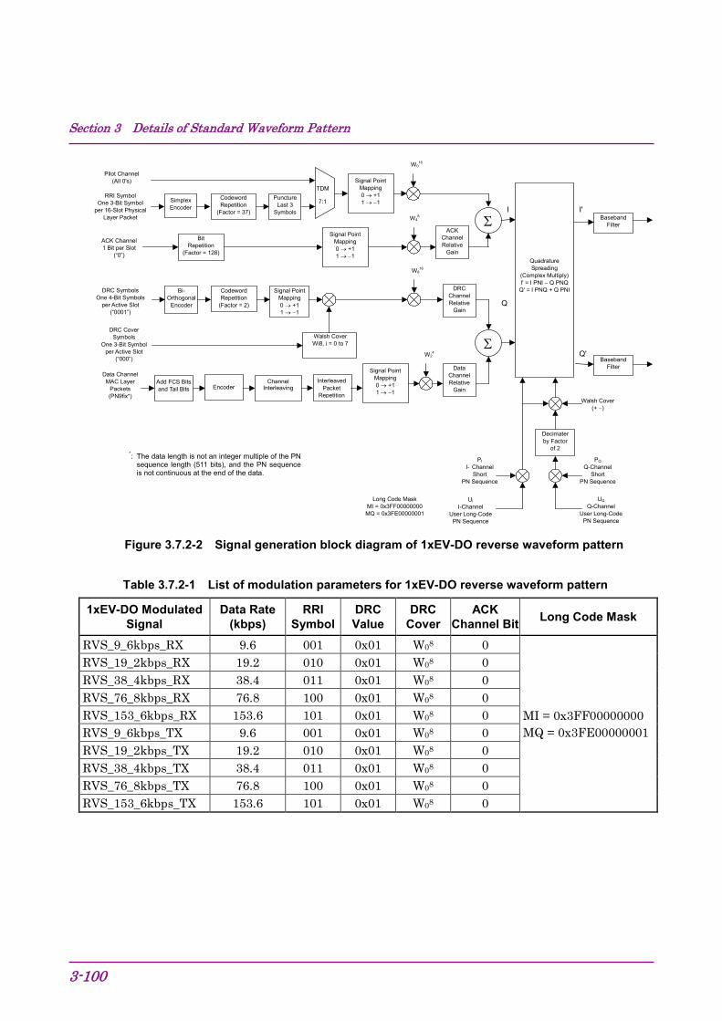
Section 3 Details of Standard Waveform Pattern
3-100
Interleaved Packet
Repetition
I
Q
Quadrature Spreading
(Complex Multiply) I' = I PNI − Q PNQ Q' = I PNQ + Q PNI
I'
Q'
Baseband Filter
Baseband Filter
UI I-Channel
User Long-Code PN Sequence
PI I- Channel
Short PN Sequence
Decimater by Factor
of 2 PQ
Q-Channel Short
PN Sequence
UQ Q-Channel
User Long-Code PN Sequence
Walsh Cover (+ −)
Σ Simplex Encoder
Codeword Repetition
(Factor = 37)
Puncture Last 3
Symbols
TDM
7:1
Signal Point Mapping 0 → +1 1 → −1
Bi- Orthogonal
Encoder
Codeword Repetition
(Factor = 2)
DRC Symbols One 4-Bit Symbols
per Active Slot (“0001”)
Signal Point Mapping 0 → +1 1 → −1
DRC Cover Symbols
One 3-Bit Symbol per Active Slot
(“000”)
RRI Symbol One 3-Bit Symbol
per 16-Slot Physical Layer Packet
Pilot Channel (All 0's)
ACK Channel 1 Bit per Slot
(“0”)
Bit Repetition
(Factor = 128)
Data Channel MAC Layer
Packets (PN9fix*)
Walsh Cover Wi8, i = 0 to 7
W016
W816
W48
W24
Signal Point Mapping 0 → +1 1 → −1
Signal Point Mapping 0 → +1 1 → −1
ACK Channel Relative
Gain
DRC Channel Relative
Gain
Data Channel Relative
Gain
Encoder Channel
Interleaving Add FCS Bits and Tail Bits
Long Code Mask MI = 0x3FF00000000 MQ = 0x3FE00000001
*: The data length is not an integer multiple of the PN sequence length (511 bits), and the PN sequence is not continuous at the end of the data.
Σ
Figure 3.7.2-2 Signal generation block diagram of 1xEV-DO reverse waveform pattern
Table 3.7.2-1 List of modulation parameters for 1xEV-DO reverse waveform pattern
1xEV-DO Modulated Signal
Data Rate (kbps)
RRI Symbol
DRC Value
DRC Cover
ACK Channel Bit Long Code Mask
RVS_9_6kbps_RX 9.6 001 0x01 W08 0
MI = 0x3FF00000000 MQ = 0x3FE00000001
RVS_19_2kbps_RX 19.2 010 0x01 W08 0 RVS_38_4kbps_RX 38.4 011 0x01 W08 0 RVS_76_8kbps_RX 76.8 100 0x01 W08 0 RVS_153_6kbps_RX 153.6 101 0x01 W08 0 RVS_9_6kbps_TX 9.6 001 0x01 W08 0 RVS_19_2kbps_TX 19.2 010 0x01 W08 0 RVS_38_4kbps_TX 38.4 011 0x01 W08 0 RVS_76_8kbps_TX 76.8 100 0x01 W08 0 RVS_153_6kbps_TX 153.6 101 0x01 W08 0
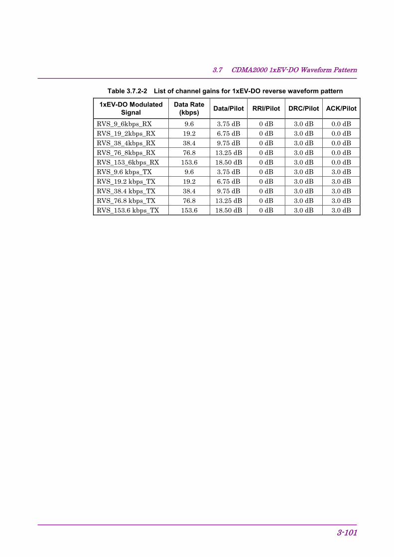
3.7 CDMA2000 1xEV-DO Waveform Pattern
3-101
Table 3.7.2-2 List of channel gains for 1xEV-DO reverse waveform pattern
1xEV-DO Modulated Signal
Data Rate (kbps) Data/Pilot RRI/Pilot DRC/Pilot ACK/Pilot
RVS_9_6kbps_RX 9.6 3.75 dB 0 dB 3.0 dB 0.0 dB RVS_19_2kbps_RX 19.2 6.75 dB 0 dB 3.0 dB 0.0 dB RVS_38_4kbps_RX 38.4 9.75 dB 0 dB 3.0 dB 0.0 dB RVS_76_8kbps_RX 76.8 13.25 dB 0 dB 3.0 dB 0.0 dB RVS_153_6kbps_RX 153.6 18.50 dB 0 dB 3.0 dB 0.0 dB RVS_9.6 kbps_TX 9.6 3.75 dB 0 dB 3.0 dB 3.0 dB RVS_19.2 kbps_TX 19.2 6.75 dB 0 dB 3.0 dB 3.0 dB RVS_38.4 kbps_TX 38.4 9.75 dB 0 dB 3.0 dB 3.0 dB RVS_76.8 kbps_TX 76.8 13.25 dB 0 dB 3.0 dB 3.0 dB RVS_153.6 kbps_TX 153.6 18.50 dB 0 dB 3.0 dB 3.0 dB
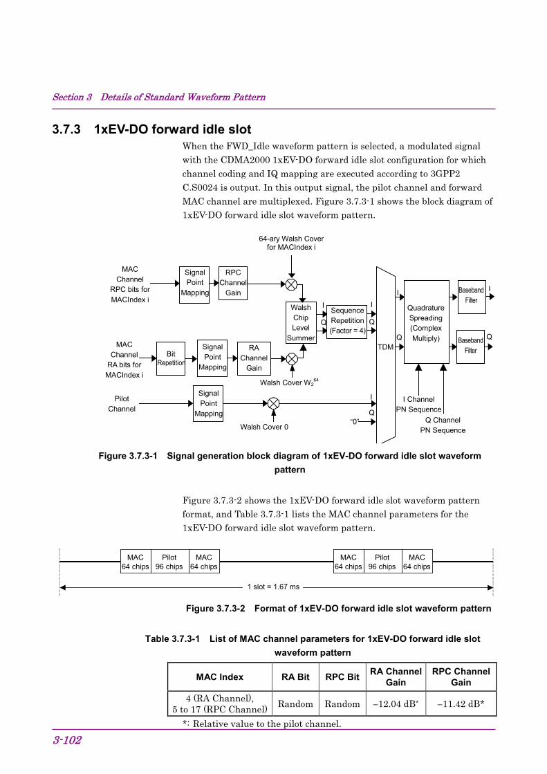
Section 3 Details of Standard Waveform Pattern
3-102
3.7.3 1xEV-DO forward idle slot When the FWD_Idle waveform pattern is selected, a modulated signal with the CDMA2000 1xEV-DO forward idle slot configuration for which channel coding and IQ mapping are executed according to 3GPP2 C.S0024 is output. In this output signal, the pilot channel and forward MAC channel are multiplexed. Figure 3.7.3-1 shows the block diagram of 1xEV-DO forward idle slot waveform pattern.
Walsh Chip Level
Summer
Walsh Cover W264
“0”
64-ary Walsh Cover for MACIndex i
I
Q
Q I
Q
I
TDM
Signal Point
Mapping
Signal Point
Mapping
Signal Point
Mapping
RA Channel
Gain
Walsh Cover 0
Sequence Repetition (Factor = 4)
Q
I Baseband
Filter
Baseband Filter
I Channel PN Sequence
Q Channel PN Sequence
MAC Channel
RPC bits for MACIndex i
MAC Channel
RA bits for MACIndex i
Pilot Channel
RPC Channel
Gain Quadrature Spreading (Complex Multiply)
I
Q
Bit Repetition
Figure 3.7.3-1 Signal generation block diagram of 1xEV-DO forward idle slot waveform pattern
Figure 3.7.3-2 shows the 1xEV-DO forward idle slot waveform pattern format, and Table 3.7.3-1 lists the MAC channel parameters for the 1xEV-DO forward idle slot waveform pattern.
1 slot = 1.67 ms
MAC 64 chips
Pilot 96 chips
MAC 64 chips
MAC 64 chips
Pilot 96 chips
MAC 64 chips
Figure 3.7.3-2 Format of 1xEV-DO forward idle slot waveform pattern
Table 3.7.3-1 List of MAC channel parameters for 1xEV-DO forward idle slot waveform pattern
MAC Index RA Bit RPC Bit RA Channel Gain
RPC Channel Gain
4 (RA Channel), 5 to 17 (RPC Channel) Random Random −12.04 dB* −11.42 dB*
*: Relative value to the pilot channel.
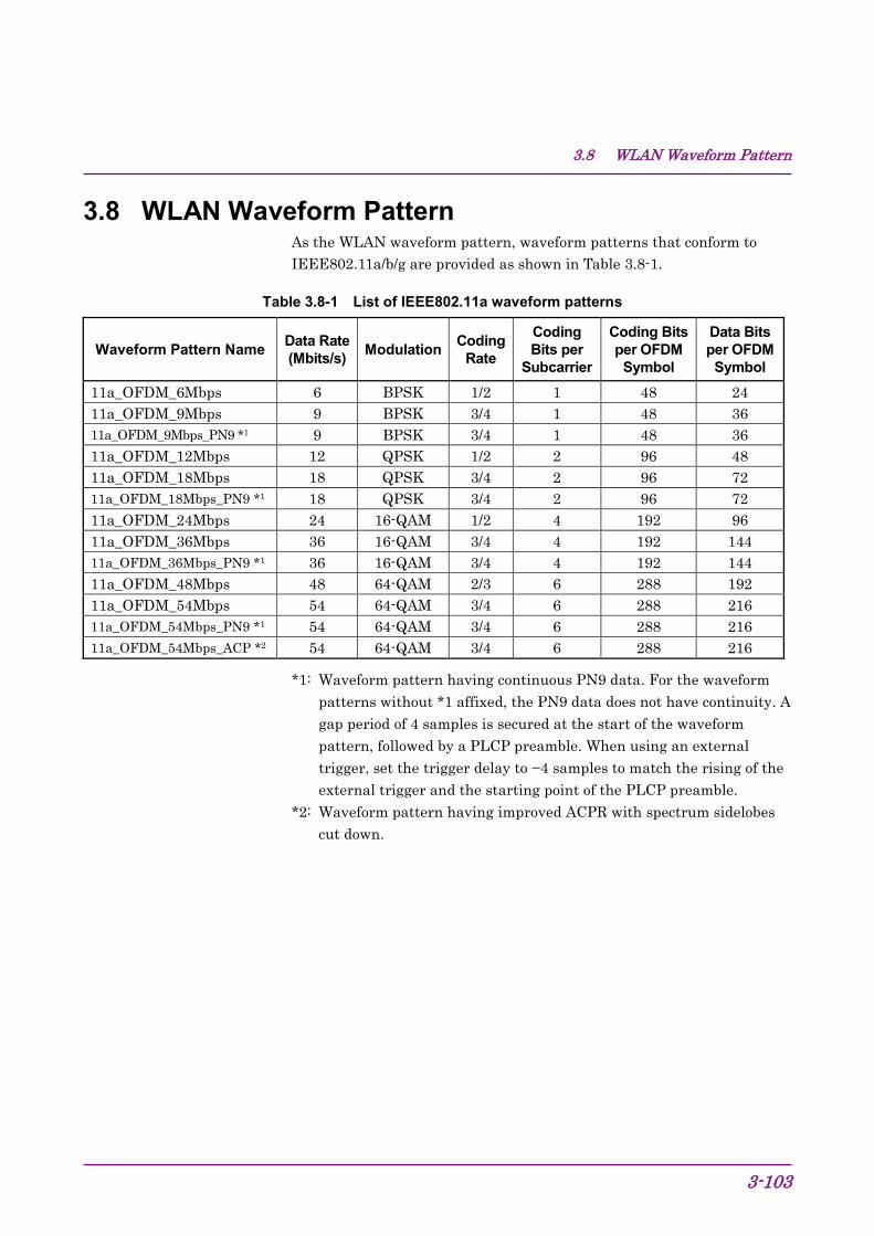
3.8 WLAN Waveform Pattern
3-103
3.8 WLAN Waveform Pattern As the WLAN waveform pattern, waveform patterns that conform to IEEE802.11a/b/g are provided as shown in Table 3.8-1.
Table 3.8-1 List of IEEE802.11a waveform patterns
Waveform Pattern Name Data Rate (Mbits/s) Modulation Coding
Rate
Coding Bits per
Subcarrier
Coding Bits per OFDM
Symbol
Data Bits per OFDM
Symbol 11a_OFDM_6Mbps 6 BPSK 1/2 1 48 24 11a_OFDM_9Mbps 9 BPSK 3/4 1 48 36 11a_OFDM_9Mbps_PN9 *1 9 BPSK 3/4 1 48 36 11a_OFDM_12Mbps 12 QPSK 1/2 2 96 48 11a_OFDM_18Mbps 18 QPSK 3/4 2 96 72 11a_OFDM_18Mbps_PN9 *1 18 QPSK 3/4 2 96 72 11a_OFDM_24Mbps 24 16-QAM 1/2 4 192 96 11a_OFDM_36Mbps 36 16-QAM 3/4 4 192 144 11a_OFDM_36Mbps_PN9 *1 36 16-QAM 3/4 4 192 144 11a_OFDM_48Mbps 48 64-QAM 2/3 6 288 192 11a_OFDM_54Mbps 54 64-QAM 3/4 6 288 216 11a_OFDM_54Mbps_PN9 *1 54 64-QAM 3/4 6 288 216 11a_OFDM_54Mbps_ACP *2 54 64-QAM 3/4 6 288 216
*1: Waveform pattern having continuous PN9 data. For the waveform patterns without *1 affixed, the PN9 data does not have continuity. A gap period of 4 samples is secured at the start of the waveform pattern, followed by a PLCP preamble. When using an external trigger, set the trigger delay to −4 samples to match the rising of the external trigger and the starting point of the PLCP preamble.
*2: Waveform pattern having improved ACPR with spectrum sidelobes cut down.
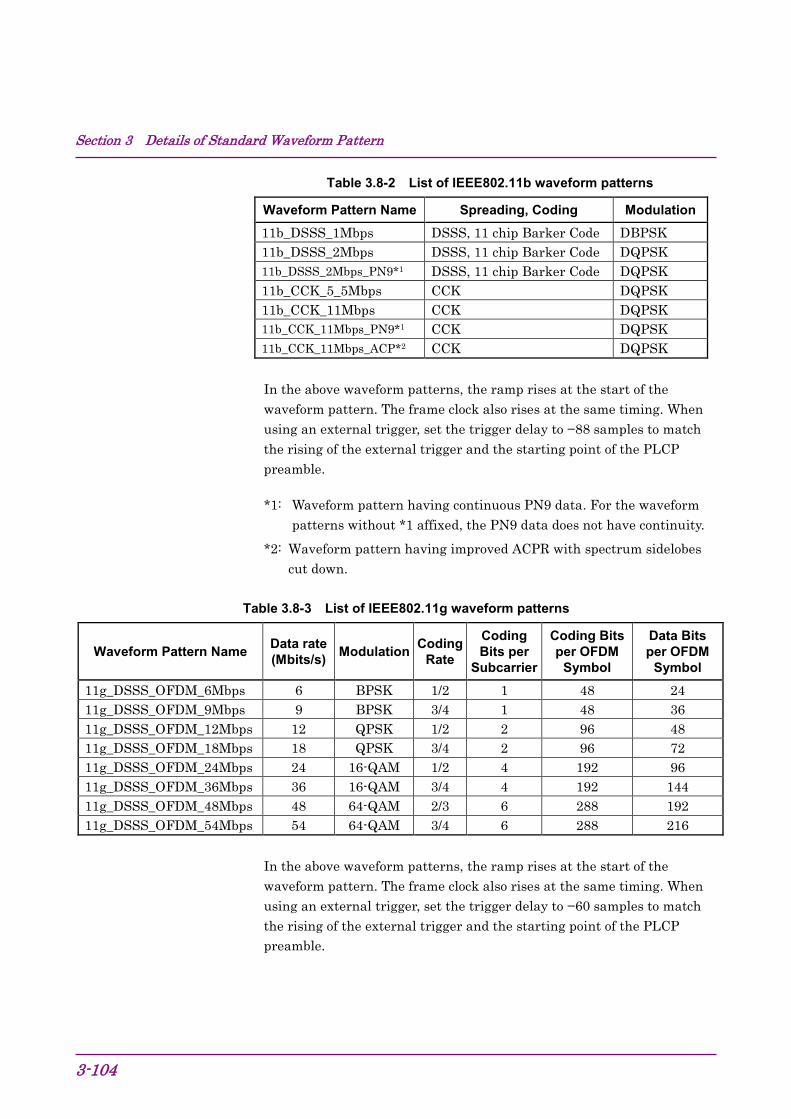
Section 3 Details of Standard Waveform Pattern
3-104
Table 3.8-2 List of IEEE802.11b waveform patterns
Waveform Pattern Name Spreading, Coding Modulation 11b_DSSS_1Mbps DSSS, 11 chip Barker Code DBPSK 11b_DSSS_2Mbps DSSS, 11 chip Barker Code DQPSK 11b_DSSS_2Mbps_PN9*1 DSSS, 11 chip Barker Code DQPSK 11b_CCK_5_5Mbps CCK DQPSK 11b_CCK_11Mbps CCK DQPSK 11b_CCK_11Mbps_PN9*1 CCK DQPSK 11b_CCK_11Mbps_ACP*2 CCK DQPSK In the above waveform patterns, the ramp rises at the start of the waveform pattern. The frame clock also rises at the same timing. When using an external trigger, set the trigger delay to −88 samples to match the rising of the external trigger and the starting point of the PLCP preamble.
*1: Waveform pattern having continuous PN9 data. For the waveform patterns without *1 affixed, the PN9 data does not have continuity.
*2: Waveform pattern having improved ACPR with spectrum sidelobes cut down.
Table 3.8-3 List of IEEE802.11g waveform patterns
Waveform Pattern Name Data rate (Mbits/s) Modulation Coding
Rate
Coding Bits per
Subcarrier
Coding Bits per OFDM
Symbol
Data Bits per OFDM
Symbol 11g_DSSS_OFDM_6Mbps 6 BPSK 1/2 1 48 24 11g_DSSS_OFDM_9Mbps 9 BPSK 3/4 1 48 36 11g_DSSS_OFDM_12Mbps 12 QPSK 1/2 2 96 48 11g_DSSS_OFDM_18Mbps 18 QPSK 3/4 2 96 72 11g_DSSS_OFDM_24Mbps 24 16-QAM 1/2 4 192 96 11g_DSSS_OFDM_36Mbps 36 16-QAM 3/4 4 192 144 11g_DSSS_OFDM_48Mbps 48 64-QAM 2/3 6 288 192 11g_DSSS_OFDM_54Mbps 54 64-QAM 3/4 6 288 216
In the above waveform patterns, the ramp rises at the start of the waveform pattern. The frame clock also rises at the same timing. When using an external trigger, set the trigger delay to −60 samples to match the rising of the external trigger and the starting point of the PLCP preamble.
3.8 WLAN Waveform Pattern
3-105
When a WLAN waveform pattern is output, a marker signal shown in Table 3.8-4 is output from the AUX connector on the rear panel of the MG3700A.
Table 3.8-4 Marker output data and IQ output level
Marker Signal Output Data Marker 1 Frame Clock Marker 2 RF Gate Marker 3 − RMS for single phase of IQ 1157 IQ output level 22 QI + = 320 mV
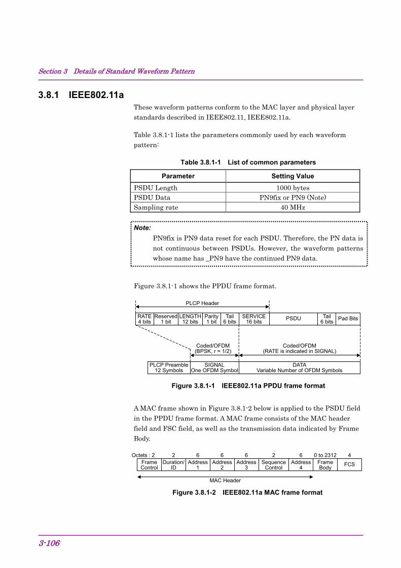
Section 3 Details of Standard Waveform Pattern
3-106
3.8.1 IEEE802.11a These waveform patterns conform to the MAC layer and physical layer standards described in IEEE802.11, IEEE802.11a.
Table 3.8.1-1 lists the parameters commonly used by each waveform pattern:
Table 3.8.1-1 List of common parameters
Parameter Setting Value
PSDU Length 1000 bytes PSDU Data PN9fix or PN9 (Note) Sampling rate 40 MHz Note:
PN9fix is PN9 data reset for each PSDU. Therefore, the PN data is not continuous between PSDUs. However, the waveform patterns whose name has _PN9 have the continued PN9 data.
Figure 3.8.1-1 shows the PPDU frame format.
RATE 4 bits
Reserved 1 bit
LENGTH 12 bits
Parity 1 bit
Tail 6 bits
SERVICE 16 bits PSDU Pad Bits Tail
6 bits
PLCP Header
PLCP Preamble 12 Symbols
SIGNAL One OFDM Symbol
DATA Variable Number of OFDM Symbols
Coded/OFDM (BPSK, r = 1/2)
Coded/OFDM (RATE is indicated in SIGNAL)
Figure 3.8.1-1 IEEE802.11a PPDU frame format
A MAC frame shown in Figure 3.8.1-2 below is applied to the PSDU field in the PPDU frame format. A MAC frame consists of the MAC header field and FSC field, as well as the transmission data indicated by Frame Body.
Frame Control
Duration/ ID
Address 1
Address 2
Address 3
Sequence Control
Address 4
Frame Body FCS
Octets : 2 2 6 6 6 2 6 0 to 2312 4
MAC Header
Figure 3.8.1-2 IEEE802.11a MAC frame format
3.8 WLAN Waveform Pattern
3-107
The Frame Control field consists of the following bits with the corresponding data as shown in Table 3.8.1-2 below.
Table 3.8.1-2 Contents of Frame Control field
Field Bit Data Protocol Version B0 and B1 00 Type B2 and B3 01 Subtype B4 to B7 0000 To DS B8 0 From DS B9 0 More Flag B10 0 Retry B11 0 Power Management B12 00 More Data B13 0 WEP B14 0 Order B15 0
Table 3.8.1-3 lists the data in a MAC header excluding the Frame Control field.
Table 3.8.1-3 Contents of MAC header excluding Frame Control field
Field Data
Duration/ID 0000H Address 1 FFFF FFFF FFFFH (Note) Address 2 0000 0000 0000H Address 3 0000 0000 0000H Sequence Control 0000H Address 4 0000 0000 0000H
Note: For Address 1 (Destination Address in the Adhoc mode,) all “1” indicates broadcast address.
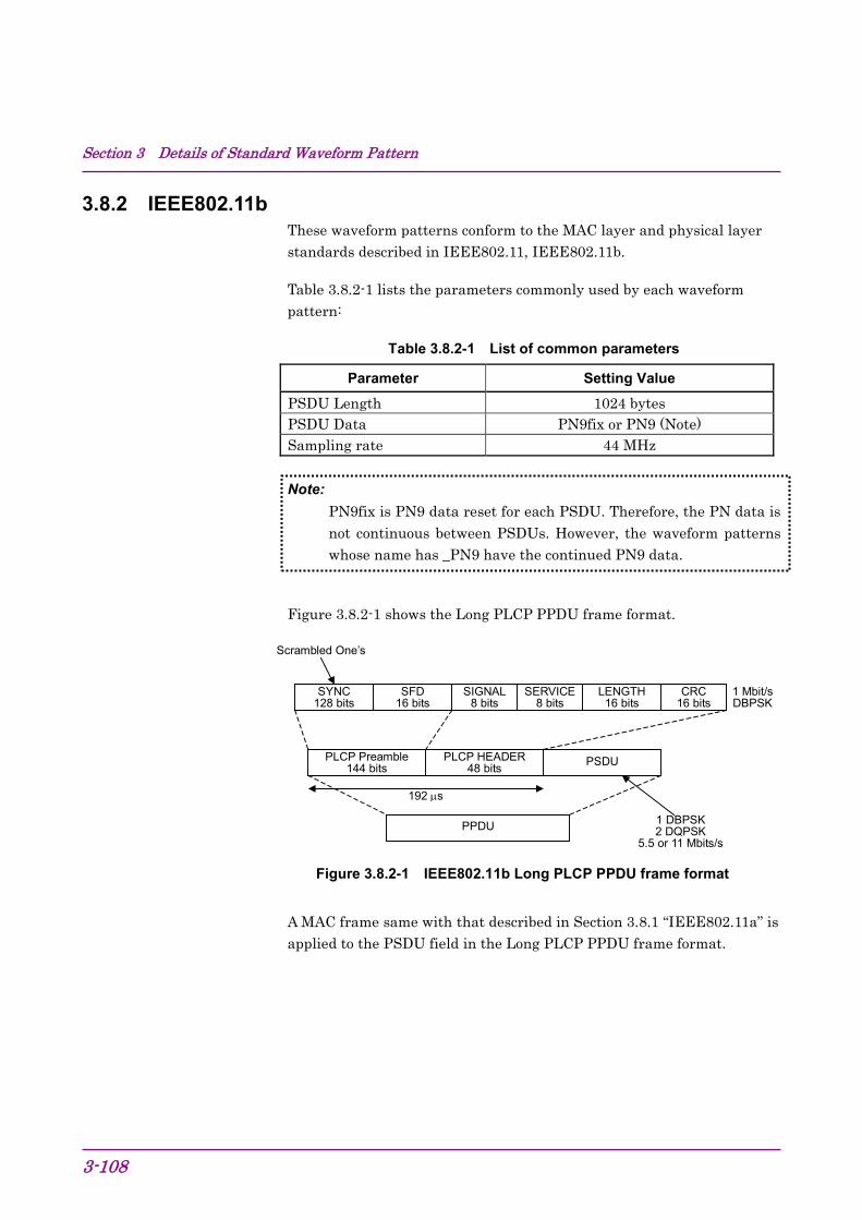
Section 3 Details of Standard Waveform Pattern
3-108
3.8.2 IEEE802.11b These waveform patterns conform to the MAC layer and physical layer standards described in IEEE802.11, IEEE802.11b.
Table 3.8.2-1 lists the parameters commonly used by each waveform pattern:
Table 3.8.2-1 List of common parameters
Parameter Setting Value
PSDU Length 1024 bytes PSDU Data PN9fix or PN9 (Note) Sampling rate 44 MHz Note:
PN9fix is PN9 data reset for each PSDU. Therefore, the PN data is not continuous between PSDUs. However, the waveform patterns whose name has _PN9 have the continued PN9 data.
Figure 3.8.2-1 shows the Long PLCP PPDU frame format.
SYNC 128 bits
SFD 16 bits
CRC 16 bits
SIGNAL 8 bits
SERVICE 8 bits
LENGTH 16 bits
PPDU
PSDU PLCP Preamble 144 bits
PLCP HEADER 48 bits
1 Mbit/s DBPSK
Scrambled One’s
192 µs
1 DBPSK 2 DQPSK
5.5 or 11 Mbits/s
Figure 3.8.2-1 IEEE802.11b Long PLCP PPDU frame format
A MAC frame same with that described in Section 3.8.1 “IEEE802.11a” is applied to the PSDU field in the Long PLCP PPDU frame format.
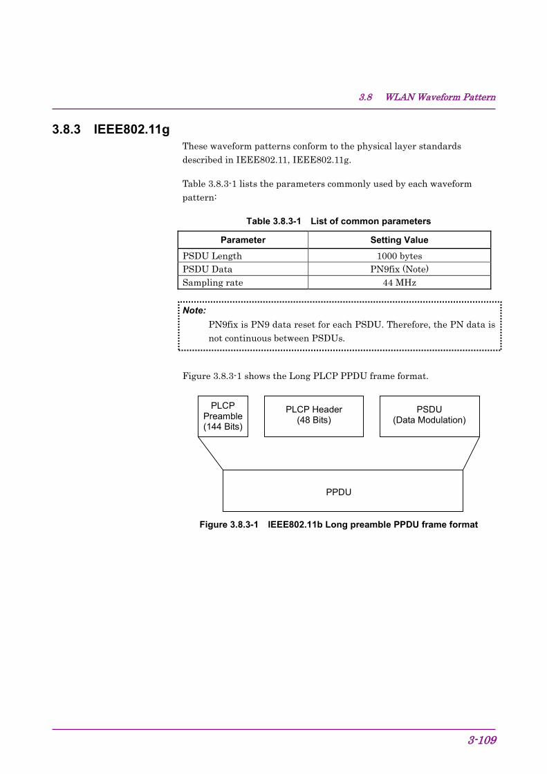
3.8 WLAN Waveform Pattern
3-109
3.8.3 IEEE802.11g These waveform patterns conform to the physical layer standards described in IEEE802.11, IEEE802.11g.
Table 3.8.3-1 lists the parameters commonly used by each waveform pattern:
Table 3.8.3-1 List of common parameters
Parameter Setting Value
PSDU Length 1000 bytes PSDU Data PN9fix (Note) Sampling rate 44 MHz Note:
PN9fix is PN9 data reset for each PSDU. Therefore, the PN data is not continuous between PSDUs.
Figure 3.8.3-1 shows the Long PLCP PPDU frame format.
PLCP Preamble (144 Bits)
PLCP Header (48 Bits)
PSDU (Data Modulation)
PPDU
Figure 3.8.3-1 IEEE802.11b Long preamble PPDU frame format
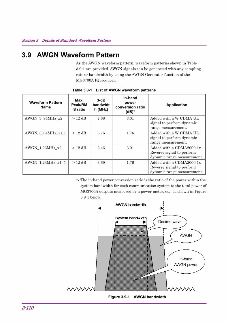
Section 3 Details of Standard Waveform Pattern
3-110
3.9 AWGN Waveform Pattern As the AWGN waveform pattern, waveform patterns shown in Table 3.9-1 are provided. AWGN signals can be generated with any sampling rate or bandwidth by using the AWGN Generator function of the MG3700A IQproducer.
Table 3.9-1 List of AWGN waveform patterns
Waveform Pattern Name
Max. Peak/RMS ratio
3-dB bandwidth (MHz)
In-band power
conversion ratio (dB)*
Application
AWGN_3_84MHz_x2 > 12 dB 7.68 3.01 Added with a W-CDMA UL signal to perform dynamic range measurement.
AWGN_3_84MHz_x1_5 > 12 dB 5.76 1.76 Added with a W-CDMA UL signal to perform dynamic range measurement.
AWGN_1.23MHz_x2 > 12 dB 2.46 3.01 Added with a CDMA2000 1x Reverse signal to perform dynamic range measurement.
AWGN_1.23MHz_x1_5 > 12 dB 3.69 1.76 Added with a CDMA2000 1x Reverse signal to perform dynamic range measurement.
*: The in-band power conversion ratio is the ratio of the power within the system bandwidth for each communication system to the total power of MG3700A outputs measured by a power meter, etc. as shown in Figure 3.9-1 below.
Figure 3.9-1 AWGN bandwidth
3.10 Digital Broadcast Waveform Pattern
3-111
3.10 Digital Broadcast Waveform Pattern The Digital Broadcast waveform patterns shown in Table 3.10-1 are provided.
Table 3.10-1 List of Digital Broadcast waveform patterns
Waveform Pattern Name Parameter Application
BS_1ch Roll-off factor: 0.35 Nyquist Bandwidth: 28.86 MHz Modulation: QPSK
Physical layer waveform pattern of digital BS broadcast for device evaluation.
CS_1ch Roll-off factor: 0.35 Nyquist Bandwidth: 21.096 MHz Modulation: QPSK
Physical layer waveform pattern of digital CS broadcast for device evaluation.
CATV_AnnexC_1ch Roll-off factor: 0.13 Nyquist Bandwidth: 5.274 MHz Modulation: 64QAM
Physical layer waveform pattern of CATV (ITU-T J83 Annex C) for device evaluation.
ISDBT_1layer_1ch Mode: 3, GI: 1/8 A-Layer:13seg, 64QAM
Physical layer waveform pattern of ISDB-T for device evaluation.
ISDBT_2layer_1ch Mode: 3, GI: 1/8 A-Layer: 1seg, QPSK B-Layer: 12seg, 64QAM
Physical layer waveform pattern of ISDB-T for device evaluation.
ISDBT_2layer_Movie Mode: 3, GI: 1/8 A-Layer: 1seg, QPSK, CR = 2/3, TI = 2 B-Layer: 12seg, 64QAM, CR = 7/8, TI = 2
Waveform pattern for ISDB-T partial reception, mainly used for evaluation of image and voice data of terminals. The waveform length is 40 frames.* ISDBT_2layer_Movie2
Mode: 3, GI: 1/8 A-Layer: 1seg, QPSK, CR = 2/3, TI = 4 B-Layer: 12seg, 64QAM, CR = 3/4, TI = 2
ISDBT_2layer_Coded
Mode: 3, GI: 1/8 A-Layer: 1seg, QPSK, CR = 2/3, TI = 2 B-Layer: 12seg, 64QAM, CR = 7/8, TI = 2
Waveform pattern for ISDB-T partial reception, mainly used for simple BER measurement. The waveform length is 4 frames.
ISDBT_QPSK_1_2 Mode: 3, GI: 1/8 A-Layer: 1seg, QPSK, CR = 1/2, TI = 0 B-Layer: 12seg, 64QAM, CR = 7/8, TI = 1
Waveform pattern for ISDB-T partial reception, mainly used for simple BER measurement. The waveform length is 4 frames. ISDBT_QPSK_2_3
Mode: 3, GI: 1/8 A-Layer: 1seg, QPSK, CR = 2/3, TI = 0 B-Layer: 12seg, 64QAM, CR = 7/8, TI =1
ISDBT_16QAM_1_2 Mode: 3, GI: 1/8 A-Layer: 1seg, 16QAM, CR = 1/2, TI = 0 B-Layer: 12seg, 64QAM, CR = 7/8, TI = 1
ISDBT_QPSK_2_3_TI4 Mode: 3, GI: 1/8 A-Layer: 1seg, QPSK, CR = 2/3, TI = 4 B-Layer: 12seg, 64QAM, CR = 3/4, TI = 2
Section 3 Details of Standard Waveform Pattern
3-112
Table 3.10-1 List of Digital Broadcast waveform patterns (Cont’d)
Waveform Pattern Name Parameter Application
ISDBTsb_Movie
Seg#1 to #5: 8-segment concatenation transmission in 1-segment format
Seg#6 to #8: 8-segment concatenation transmission in 3-segment format
Mode: 3, GI: 1/8 A-Layer: QPSK, CR = 1/2, TI = 4 B-Layer: QPSK, CR = 1/2, TI = 4
Mainly used for evaluation of image and voice data of terminals. The waveform length is 68 frames.*
ISDBTsb_QPSK_1_2
Seg#1 to #5: 8-segment concatenation transmission in 1-segment format
Seg#6 to #8: 8-segment concatenation transmission in 3-segment format
Mode: 3, GI: 1/8 A-Layer: QPSK, CR = 1/2, TI = 0 B-Layer: QPSK, CR = 1/2, TI = 0
Mainly used for simple BER measurement. The waveform length is 4 frames.
ISDBTsb_QPSK_2_3
Seg#1 to #5: 8-segment concatenation transmission in 1-segment format
Seg#6 to #8: 8-segment concatenation transmission in 3-segment format
Mode: 3, GI: 1/8 A-Layer: QPSK, CR = 2/3, TI = 0 B-Layer: QPSK, CR = 2/3, TI = 0
ISDBTsb_16QAM_1_2
Seg#1 to #5: 8-segment concatenation transmission in 1-segment format
Seg#6 to #8: 8-segment concatenation transmission in 3-segment format
Mode: 3, GI: 1/8 A-Layer: 16QAM, CR = 1/2, TI = 0 B-Layer: 16QAM, CR = 1/2, TI = 0
*: It is not guaranteed that any receiver can receive a waveform with this length.
3.10 Digital Broadcast Waveform Pattern
3-113
Table 3.10-2 lists the parameters commonly used by each waveform pattern.
Table 3.10-2 List of common parameters
Parameter Setting Value
Data PN23fix*: (digital BS, digital CS, CATV, ISDB-T)
Sampling rate
digital BS: 144.3 Msps digital CS: 147.62 Msps CATV: 42.192 Msps ISDB-T: 16.253968 Msps ISDB-Tsb: 8.12698417 Msps
RMS for single phase of IQ 1157
IQ output level 22 QI + = 320 mV
*: PN sequence is discontinuous at the connection of the waveform pattern.
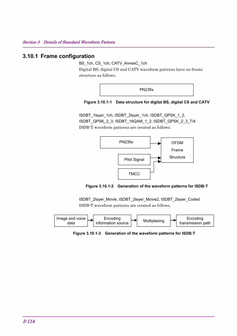
Section 3 Details of Standard Waveform Pattern
3-114
3.10.1 Frame configuration BS_1ch, CS_1ch, CATV_AnnexC_1ch Digital BS, digital CS and CATV waveform patterns have no-frame structure as follows.
PN23fix
Figure 3.10.1-1 Data structure for digital BS, digital CS and CATV
ISDBT_1layer_1ch, ISDBT_2layer_1ch, ISDBT_QPSK_1_2, ISDBT_QPSK_2_3, ISDBT_16QAM_1_2, ISDBT_QPSK_2_3_TI4 ISDB-T waveform patterns are created as follows.
PN23fix
Pilot Signal
TMCC
OFDM
Frame
Structure
Figure 3.10.1-2 Generation of the waveform patterns for ISDB-T
ISDBT_2layer_Movie, ISDBT_2layer_Movie2, ISDBT_2layer_Coded ISDB-T waveform patterns are created as follows.
Image and voice data
Encoding information source Multiplexing Encoding
transmission path
Figure 3.10.1-3 Generation of the waveform patterns for ISDB-T
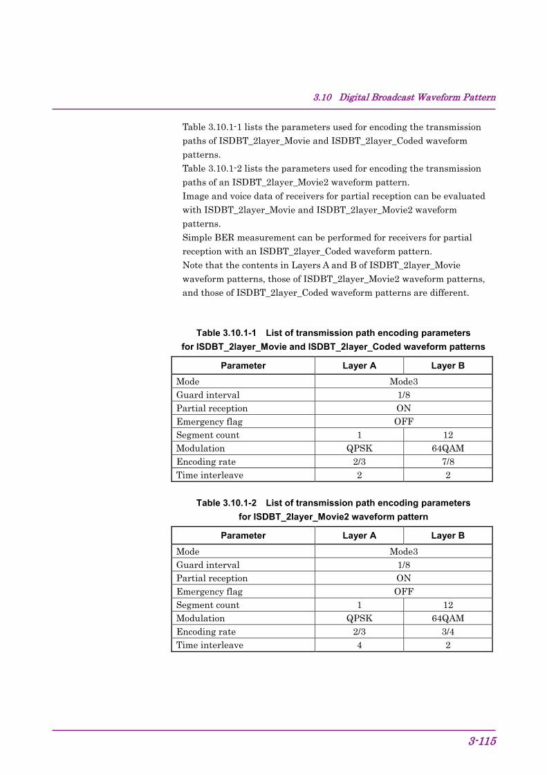
3.10 Digital Broadcast Waveform Pattern
3-115
Table 3.10.1-1 lists the parameters used for encoding the transmission paths of ISDBT_2layer_Movie and ISDBT_2layer_Coded waveform patterns. Table 3.10.1-2 lists the parameters used for encoding the transmission paths of an ISDBT_2layer_Movie2 waveform pattern. Image and voice data of receivers for partial reception can be evaluated with ISDBT_2layer_Movie and ISDBT_2layer_Movie2 waveform patterns. Simple BER measurement can be performed for receivers for partial reception with an ISDBT_2layer_Coded waveform pattern. Note that the contents in Layers A and B of ISDBT_2layer_Movie waveform patterns, those of ISDBT_2layer_Movie2 waveform patterns, and those of ISDBT_2layer_Coded waveform patterns are different.
Table 3.10.1-1 List of transmission path encoding parameters for ISDBT_2layer_Movie and ISDBT_2layer_Coded waveform patterns
Parameter Layer A Layer B Mode Mode3 Guard interval 1/8 Partial reception ON Emergency flag OFF Segment count 1 12 Modulation QPSK 64QAM Encoding rate 2/3 7/8 Time interleave 2 2
Table 3.10.1-2 List of transmission path encoding parameters
for ISDBT_2layer_Movie2 waveform pattern
Parameter Layer A Layer B
Mode Mode3 Guard interval 1/8 Partial reception ON Emergency flag OFF Segment count 1 12 Modulation QPSK 64QAM Encoding rate 2/3 3/4 Time interleave 4 2
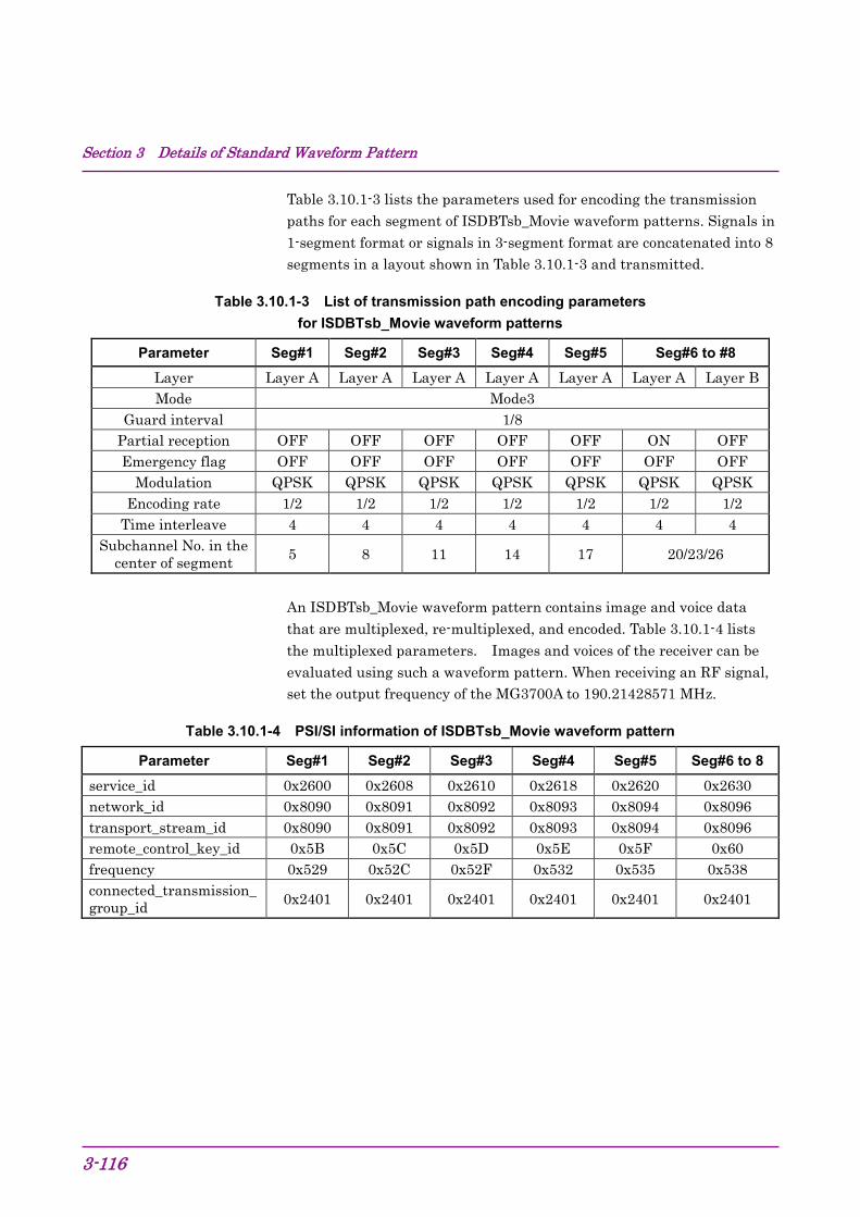
Section 3 Details of Standard Waveform Pattern
3-116
Table 3.10.1-3 lists the parameters used for encoding the transmission paths for each segment of ISDBTsb_Movie waveform patterns. Signals in 1-segment format or signals in 3-segment format are concatenated into 8 segments in a layout shown in Table 3.10.1-3 and transmitted.
Table 3.10.1-3 List of transmission path encoding parameters for ISDBTsb_Movie waveform patterns
Parameter Seg#1 Seg#2 Seg#3 Seg#4 Seg#5 Seg#6 to #8 Layer Layer A Layer A Layer A Layer A Layer A Layer A Layer B Mode Mode3
Guard interval 1/8 Partial reception OFF OFF OFF OFF OFF ON OFF Emergency flag OFF OFF OFF OFF OFF OFF OFF
Modulation QPSK QPSK QPSK QPSK QPSK QPSK QPSK Encoding rate 1/2 1/2 1/2 1/2 1/2 1/2 1/2
Time interleave 4 4 4 4 4 4 4 Subchannel No. in the
center of segment 5 8 11 14 17 20/23/26
An ISDBTsb_Movie waveform pattern contains image and voice data that are multiplexed, re-multiplexed, and encoded. Table 3.10.1-4 lists the multiplexed parameters. Images and voices of the receiver can be evaluated using such a waveform pattern. When receiving an RF signal, set the output frequency of the MG3700A to 190.21428571 MHz.
Table 3.10.1-4 PSI/SI information of ISDBTsb_Movie waveform pattern
Parameter Seg#1 Seg#2 Seg#3 Seg#4 Seg#5 Seg#6 to 8 service_id 0x2600 0x2608 0x2610 0x2618 0x2620 0x2630 network_id 0x8090 0x8091 0x8092 0x8093 0x8094 0x8096 transport_stream_id 0x8090 0x8091 0x8092 0x8093 0x8094 0x8096 remote_control_key_id 0x5B 0x5C 0x5D 0x5E 0x5F 0x60 frequency 0x529 0x52C 0x52F 0x532 0x535 0x538 connected_transmission_group_id 0x2401 0x2401 0x2401 0x2401 0x2401 0x2401
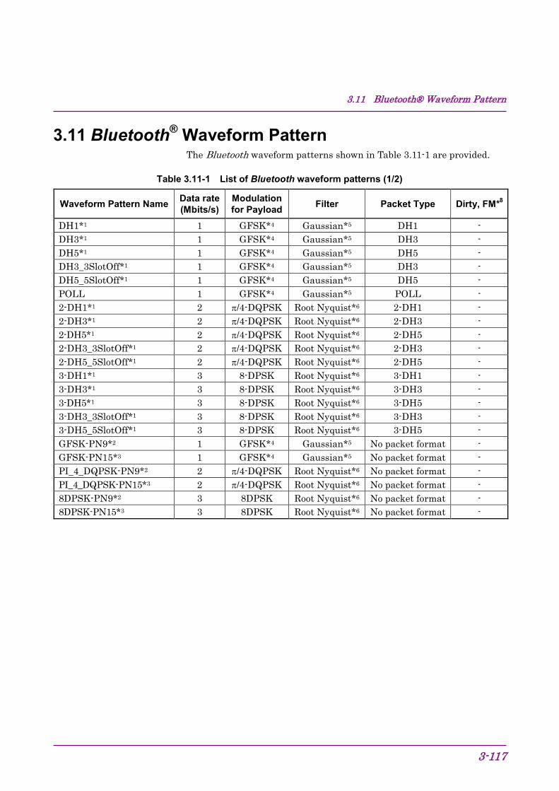
3.11 Bluetooth® Waveform Pattern
3-117
3.11 Bluetooth® Waveform Pattern The Bluetooth waveform patterns shown in Table 3.11-1 are provided.
Table 3.11-1 List of Bluetooth waveform patterns (1/2)
Waveform Pattern Name Data rate (Mbits/s)
Modulation for Payload Filter Packet Type Dirty, FM*8
DH1*1 1 GFSK*4 Gaussian*5 DH1 - DH3*1 1 GFSK*4 Gaussian*5 DH3 - DH5*1 1 GFSK*4 Gaussian*5 DH5 - DH3_3SlotOff*1 1 GFSK*4 Gaussian*5 DH3 - DH5_5SlotOff*1 1 GFSK*4 Gaussian*5 DH5 - POLL 1 GFSK*4 Gaussian*5 POLL - 2-DH1*1 2 π/4-DQPSK Root Nyquist*6 2-DH1 - 2-DH3*1 2 π/4-DQPSK Root Nyquist*6 2-DH3 - 2-DH5*1 2 π/4-DQPSK Root Nyquist*6 2-DH5 - 2-DH3_3SlotOff*1 2 π/4-DQPSK Root Nyquist*6 2-DH3 - 2-DH5_5SlotOff*1 2 π/4-DQPSK Root Nyquist*6 2-DH5 - 3-DH1*1 3 8-DPSK Root Nyquist*6 3-DH1 - 3-DH3*1 3 8-DPSK Root Nyquist*6 3-DH3 - 3-DH5*1 3 8-DPSK Root Nyquist*6 3-DH5 - 3-DH3_3SlotOff*1 3 8-DPSK Root Nyquist*6 3-DH3 - 3-DH5_5SlotOff*1 3 8-DPSK Root Nyquist*6 3-DH5 - GFSK-PN9*2 1 GFSK*4 Gaussian*5 No packet format - GFSK-PN15*3 1 GFSK*4 Gaussian*5 No packet format - PI_4_DQPSK-PN9*2 2 π/4-DQPSK Root Nyquist*6 No packet format - PI_4_DQPSK-PN15*3 2 π/4-DQPSK Root Nyquist*6 No packet format - 8DPSK-PN9*2 3 8DPSK Root Nyquist*6 No packet format - 8DPSK-PN15*3 3 8DPSK Root Nyquist*6 No packet format -
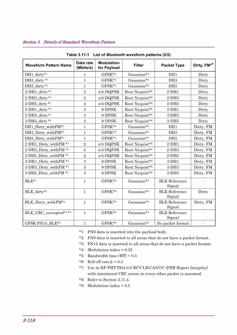
Section 3 Details of Standard Waveform Pattern
3-118
Table 3.11-1 List of Bluetooth waveform patterns (2/2)
Waveform Pattern Name Data rate (Mbits/s)
Modulation for Payload Filter Packet Type Dirty, FM*8
DH1_dirty*1 1 GFSK*4 Gaussian*5 DH1 Dirty DH3_dirty *1 1 GFSK*4 Gaussian*5 DH3 Dirty DH5_dirty *1 1 GFSK*4 Gaussian*5 DH5 Dirty 2-DH1_dirty *1 2 π/4-DQPSK Root Nyquist*6 2-DH1 Dirty 2-DH3_dirty *1 2 π/4-DQPSK Root Nyquist*6 2-DH3 Dirty 2-DH5_dirty *1 2 π/4-DQPSK Root Nyquist*6 2-DH5 Dirty 3-DH1_dirty *1 3 8-DPSK Root Nyquist*6 3-DH1 Dirty 3-DH3_dirty *1 3 8-DPSK Root Nyquist*6 3-DH3 Dirty 3-DH5_dirty *1 3 8-DPSK Root Nyquist*6 3-DH5 Dirty DH1_Dirty_withFM*1 1 GFSK*4 Gaussian*5 DH1 Dirty, FM DH3_Dirty_withFM*1 1 GFSK*4 Gaussian*5 DH3 Dirty, FM DH5_Dirty_withFM*1 1 GFSK*4 Gaussian*5 DH5 Dirty, FM 2-DH1_Dirty_withFM *1 2 π/4-DQPSK Root Nyquist*6 2-DH1 Dirty, FM 2-DH3_Dirty_withFM *1 2 π/4-DQPSK Root Nyquist*6 2-DH3 Dirty, FM 2-DH5_Dirty_withFM *1 2 π/4-DQPSK Root Nyquist*6 2-DH5 Dirty, FM 3-DH1_Dirty_withFM *1 3 8-DPSK Root Nyquist*6 3-DH1 Dirty, FM 3-DH3_Dirty_withFM *1 3 8-DPSK Root Nyquist*6 3-DH3 Dirty, FM 3-DH5_Dirty_withFM *1 3 8-DPSK Root Nyquist*6 3-DH5 Dirty, FM
BLE*1 1 GFSK*9 Gaussian*5 BLE Reference Signal
-
BLE_dirty*1 1 GFSK*9 Gaussian*5 BLE Reference Signal
Dirty
BLE_Dirty_withFM*1 1 GFSK*9 Gaussian*5 BLE Reference Signal
Dirty, FM
BLE_CRC_corrupted*1,*7 1 GFSK*9 Gaussian*5 BLE Reference Signal
-
GFSK-PN15_BLE*3 1 GFSK*9 Gaussian*5 No packet format -
*1: PN9 data is inserted into the payload body. *2: PN9 data is inserted to all areas that do not have a packet format. *3: PN15 data is inserted to all areas that do not have a packet format. *4: Modulation index = 0.32 *5: Bandwidth time (BT) = 0.5 *6: Roll-off rate β = 0.4 *7: Use in RF-PHY.TS/4.0.0 RCV-LE/CA/07/C (PER Report Integrity)
with intentional CRC errors in every other packet is assumed. *8: Refer to Section 3.11.4. *9: Modulation index = 0.5
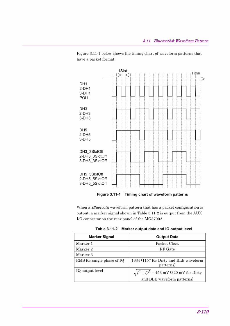
3.11 Bluetooth® Waveform Pattern
3-119
Figure 3.11-1 below shows the timing chart of waveform patterns that have a packet format.
DH12-DH13-DH1POLL
DH32-DH33-DH3
DH52-DH53-DH5
1Slot Time
DH3_3SlotOff2-DH3_3SlotOff3-DH3_3SlotOff
DH5_5SlotOff2-DH5_5SlotOff3-DH5_5SlotOff
Figure 3.11-1 Timing chart of waveform patterns
When a Bluetooth waveform pattern that has a packet configuration is output, a marker signal shown in Table 3.11-2 is output from the AUX I/O connector on the rear panel of the MG3700A.
Table 3.11-2 Marker output data and IQ output level
Marker Signal Output Data Marker 1 Packet Clock Marker 2 RF Gate Marker 3 − RMS for single phase of IQ 1634 (1157 for Dirty and BLE waveform
patterns) IQ output level 22 QI + = 453 mV (320 mV for Dirty
and BLE waveform patterns)
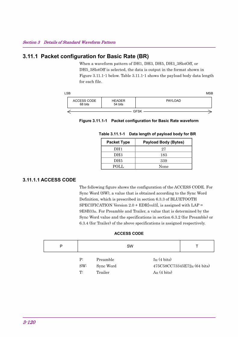
Section 3 Details of Standard Waveform Pattern
3-120
3.11.1 Packet configuration for Basic Rate (BR) When a waveform pattern of DH1, DH3, DH5, DH3_3SlotOff, or DH5_5SlotOff is selected, the data is output in the format shown in Figure 3.11.1-1 below. Table 3.11.1-1 shows the payload body data length for each file.
LSB MSB
GFSK
HEADER 54 bits
ACCESS CODE 68 bits
PAYLOAD
Figure 3.11.1-1 Packet configuration for Basic Rate waveform
Table 3.11.1-1 Data length of payload body for BR
Packet Type Payload Body (Bytes) DH1 27 DH3 183 DH5 339
POLL None
3.11.1.1 ACCESS CODE The following figure shows the configuration of the ACCESS CODE. For Sync Word (SW), a value that is obtained according to the Sync Word Definition, which is prescribed in section 6.3.3 of BLUETOOTH SPECIFICATION Version 2.0 + EDR[vol3], is assigned with LAP = 9E8B33H. For Preamble and Trailer, a value that is determined by the Sync Word value and the specifications in section 6.3.2 (for Preamble) or 6.3.4 (for Trailer) of the above specifications is assigned respectively.
ACCESS CODE
P SW T
P: Preamble 5H (4 bits) SW: Sync Word 475C58CC73345E72H (64 bits) T: Trailer AH (4 bits)
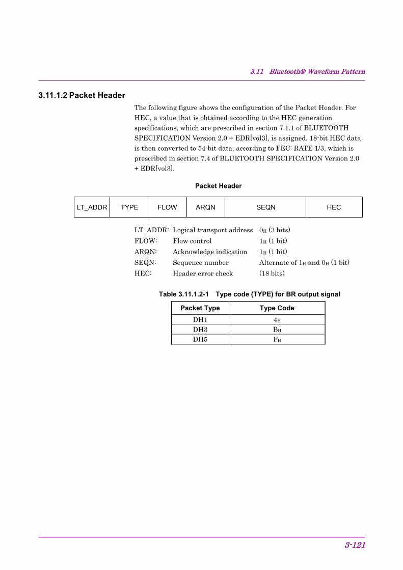
3.11 Bluetooth® Waveform Pattern
3-121
3.11.1.2 Packet Header The following figure shows the configuration of the Packet Header. For HEC, a value that is obtained according to the HEC generation specifications, which are prescribed in section 7.1.1 of BLUETOOTH SPECIFICATION Version 2.0 + EDR[vol3], is assigned. 18-bit HEC data is then converted to 54-bit data, according to FEC: RATE 1/3, which is prescribed in section 7.4 of BLUETOOTH SPECIFICATION Version 2.0 + EDR[vol3].
Packet Header
LT_ADDR ARQN HEC TYPE FLOW SEQN
LT_ADDR: Logical transport address 0H (3 bits) FLOW: Flow control 1H (1 bit) ARQN: Acknowledge indication 1H (1 bit) SEQN: Sequence number Alternate of 1H and 0H (1 bit) HEC: Header error check (18 bits)
Table 3.11.1.2-1 Type code (TYPE) for BR output signal
Packet Type Type Code
DH1 4H DH3 BH DH5 FH
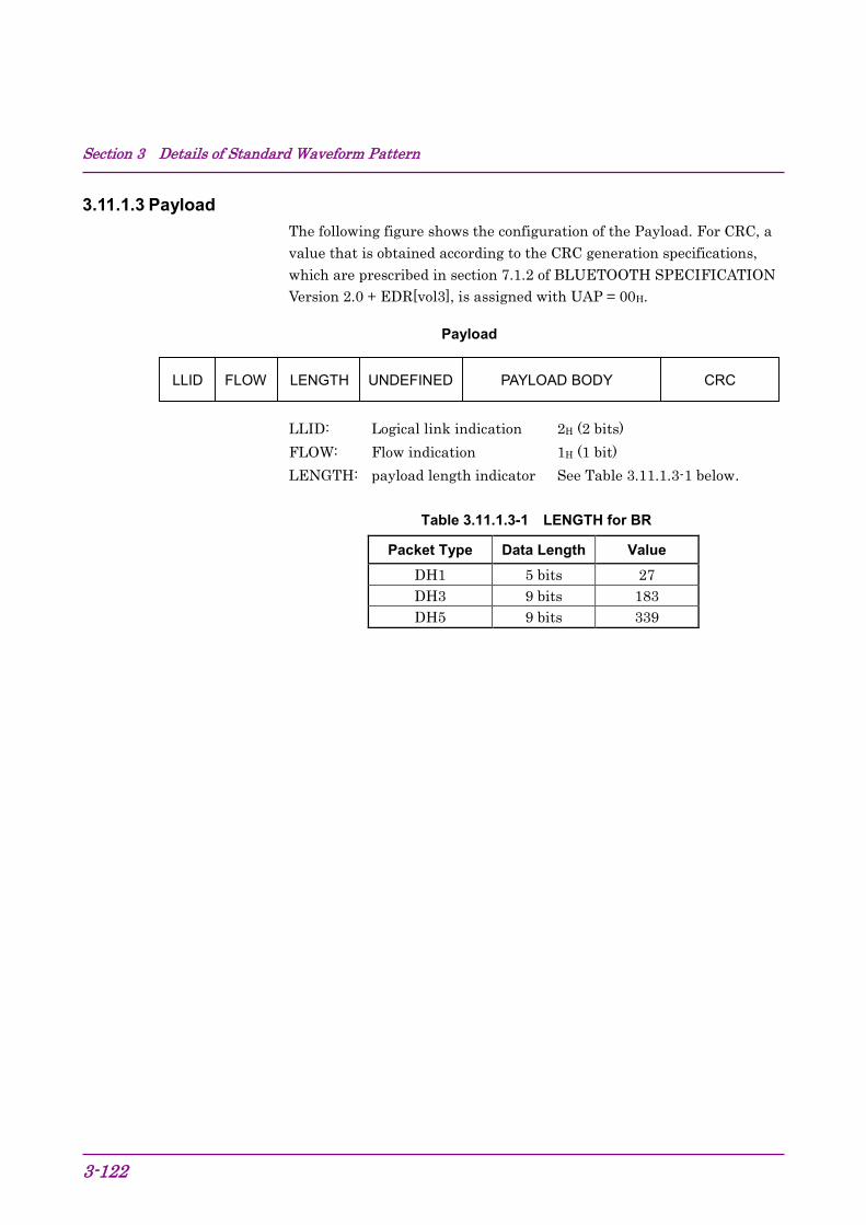
Section 3 Details of Standard Waveform Pattern
3-122
3.11.1.3 Payload The following figure shows the configuration of the Payload. For CRC, a value that is obtained according to the CRC generation specifications, which are prescribed in section 7.1.2 of BLUETOOTH SPECIFICATION Version 2.0 + EDR[vol3], is assigned with UAP = 00H.
Payload
LLID UNDEFINED CRC FLOW LENGTH PAYLOAD BODY
LLID: Logical link indication 2H (2 bits) FLOW: Flow indication 1H (1 bit) LENGTH: payload length indicator See Table 3.11.1.3-1 below.
Table 3.11.1.3-1 LENGTH for BR
Packet Type Data Length Value DH1 5 bits 27 DH3 9 bits 183 DH5 9 bits 339
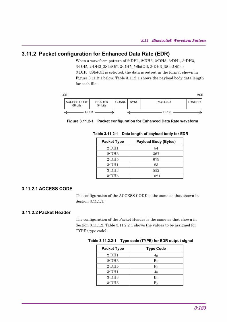
3.11 Bluetooth® Waveform Pattern
3-123
3.11.2 Packet configuration for Enhanced Data Rate (EDR) When a waveform pattern of 2-DH1, 2-DH3, 2-DH5, 3-DH1, 3-DH3, 3-DH5, 2-DH3_3SlotOff, 2-DH5_5SlotOff, 3-DH3_3SlotOff, or 3-DH5_5SlotOff is selected, the data is output in the format shown in Figure 3.11.2-1 below. Table 3.11.2-1 shows the payload body data length for each file.
LSB MSB
GUARD
SYNC
TRAILER
GFSK DPSK
HEADER 54 bits
ACCESS CODE 68 bits
PAYLOAD
Figure 3.11.2-1 Packet configuration for Enhanced Data Rate waveform
Table 3.11.2-1 Data length of payload body for EDR
Packet Type Payload Body (Bytes) 2-DH1 54 2-DH3 367 2-DH5 679 3-DH1 83 3-DH3 552 3-DH5 1021
3.11.2.1 ACCESS CODE The configuration of the ACCESS CODE is the same as that shown in Section 3.11.1.1.
3.11.2.2 Packet Header The configuration of the Packet Header is the same as that shown in Section 3.11.1.2. Table 3.11.2.2-1 shows the values to be assigned for TYPE (type code).
Table 3.11.2.2-1 Type code (TYPE) for EDR output signal
Packet Type Type Code 2-DH1 4H 2-DH3 BH 2-DH5 FH 3-DH1 4H 3-DH3 BH 3-DH5 FH
Section 3 Details of Standard Waveform Pattern
3-124
3.11.2.3 Payload The configuration of the Payload is the same as that shown in Section 3.11.1.3. Table 3.11.2.3-1 shows the data lengths and setting values for LENGTH.
Table 3.11.2.3-1 LENGTH for EDR
Packet Type Data Length Value 2-DH1 5 bits 54 2-DH3 10 bits 366 2-DH5 10 bits 678 3-DH1 5 bits 81 3-DH3 10 bits 549 3-DH5 10 bits 1017
3.11.2.4 Synchronous Sequence The following value is assigned for Synchronous Sequence (SYNC) in each EDR packet. The phase is initialized to 0 rad by setting 0 to the head of Synchronous Sequence.
For 2-DH1, 2-DH3, and 2-DH5 packets: 0777D5H (22 bits) For 3-DH1, 3-DH3, and 3-DH5 packets: 0175D7E92H (33 bits)
3.11.2.5 Trailer The following value is assigned for Trailer (TRAILER) in each EDR packet.
For 2-DH1, 2-DH3, and 2-DH5 packets: 0H (4 bits) For 3-DH1, 3-DH3, and 3-DH5 packets: 00H (6 bits)
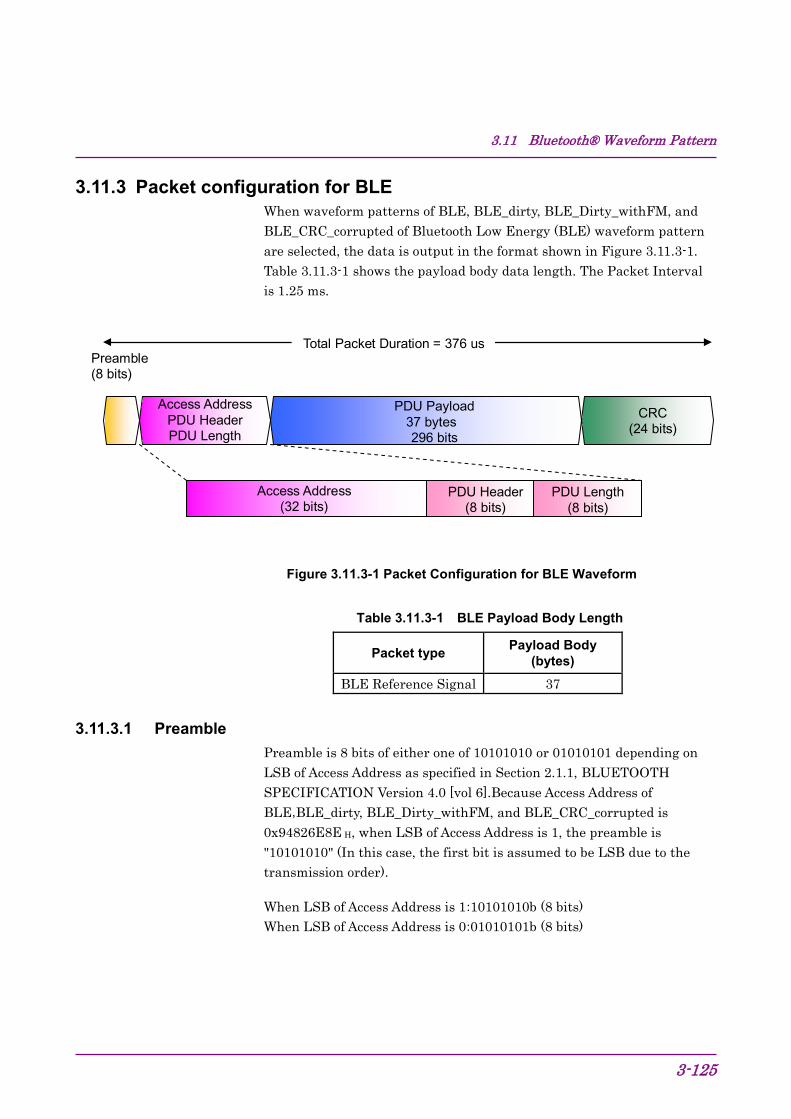
3.11 Bluetooth® Waveform Pattern
3-125
3.11.3 Packet configuration for BLE When waveform patterns of BLE, BLE_dirty, BLE_Dirty_withFM, and BLE_CRC_corrupted of Bluetooth Low Energy (BLE) waveform pattern are selected, the data is output in the format shown in Figure 3.11.3-1. Table 3.11.3-1 shows the payload body data length. The Packet Interval is 1.25 ms.
Access Address PDU Header PDU Length
Preamble (8 bits)
PDU Payload 37 bytes 296 bits
CRC (24 bits)
Access Address (32 bits)
PDU Header (8 bits)
PDU Length (8 bits)
Total Packet Duration = 376 us
Figure 3.11.3-1 Packet Configuration for BLE Waveform
Table 3.11.3-1 BLE Payload Body Length
Packet type Payload Body (bytes)
BLE Reference Signal 37
3.11.3.1 Preamble Preamble is 8 bits of either one of 10101010 or 01010101 depending on LSB of Access Address as specified in Section 2.1.1, BLUETOOTH SPECIFICATION Version 4.0 [vol 6].Because Access Address of BLE,BLE_dirty, BLE_Dirty_withFM, and BLE_CRC_corrupted is 0x94826E8E H, when LSB of Access Address is 1, the preamble is "10101010" (In this case, the first bit is assumed to be LSB due to the transmission order).
When LSB of Access Address is 1 :10101010b (8 bits) When LSB of Access Address is 0 :01010101b (8 bits)
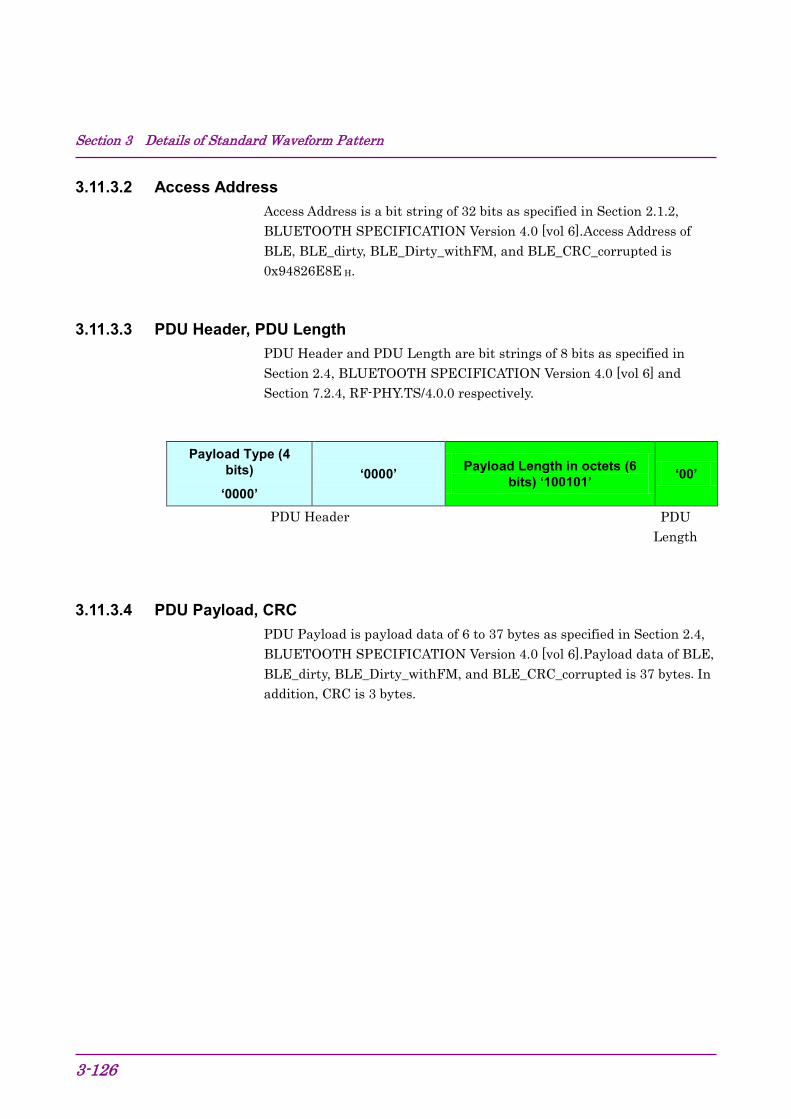
Section 3 Details of Standard Waveform Pattern
3-126
3.11.3.2 Access Address Access Address is a bit string of 32 bits as specified in Section 2.1.2, BLUETOOTH SPECIFICATION Version 4.0 [vol 6].Access Address of BLE, BLE_dirty, BLE_Dirty_withFM, and BLE_CRC_corrupted is 0x94826E8E H.
3.11.3.3 PDU Header, PDU Length PDU Header and PDU Length are bit strings of 8 bits as specified in Section 2.4, BLUETOOTH SPECIFICATION Version 4.0 [vol 6] and Section 7.2.4, RF-PHY.TS/4.0.0 respectively.
Payload Type (4 bits)
‘0000’ ‘0000’ Payload Length in octets (6
bits) ‘100101’ ‘00’
PDU Header PDU Length
3.11.3.4 PDU Payload, CRC PDU Payload is payload data of 6 to 37 bytes as specified in Section 2.4, BLUETOOTH SPECIFICATION Version 4.0 [vol 6].Payload data of BLE, BLE_dirty, BLE_Dirty_withFM, and BLE_CRC_corrupted is 37 bytes.In addition, CRC is 3 bytes.
3.11 Bluetooth® Waveform Pattern
3-127
3.11.4 Dirty Transmitter Signal Dirty Transmitter Signal is specified as a signal used for a reception test in Section 5.1.18, Bluetooth Test Specification v1.2/2.0/2.0 + EDR/2.1/2.1 + EDR/3.0/3.0 + HS and Section 6.3.1, RF-PHY.TS/4.0.0. This Dirty Transmitter Signal changes the frequency offset, modulation index, and symbol timing error with every 50 packets. 10 combinations of these three parameters are specified, and outputs of Test Run 1 to 10 are repeated. Furthermore, the frequency drift of output signals is specified for the Dirty Transmitter Signal. The waveform patterns "Dirty" in Table 3.11-1 are waveform patterns with the addition of the frequency offset, modulation index fluctuation, and symbol timing error. In addition, the waveform patterns "Dirty, FM" are signals with the addition of the frequency offset, modulation index fluctuation, symbol timing error, and frequency drift.
The Bluetooth word mark and logo are owned by Bluetooth SIG, Inc. and Anritsu uses this mark based on the license. Other trademarks and trade names shall belong to individual owners.
Section 3 Details of Standard Waveform Pattern
3-128
3.12 GPS Waveform Pattern The GPS waveform patterns shown in Table 3.12-1 are provided.
Table 3.12-1 List of GPS waveform patterns
Waveform Pattern Name Main Usage Outline of Data
SYNC_ADJ*1 Synchronization adjustment*2
Consists of TLM, HOW, and default navigation data, formatted according to the subframe configuration that is prescribed in GLOBAL POSITIONING SYSTEM STANDARD POSITIONING SERVICE SIGNAL SPECIFICATION. One period is configured with 1 subframe.
TLM*3 Sensitivity test Consists of TLM, HOW, and default navigation data, formatted according to the subframe configuration that is prescribed in GLOBAL POSITIONING SYSTEM STANDARD POSITIONING SERVICE SIGNAL SPECIFICATION.
PN9 BER measurement
Consecutive PN9 data, not configured in a subframe format
PARITY Parity detection Configured in the Word format that is prescribed in GLOBAL POSITIONING SYSTEM STANDARD POSITIONING SERVICE SIGNAL SPECIFICATION. One Word consists of 24-bit PN9fix data and 6-bit parity bit data.
TLM_PARITY Sensitivity test Consists of TLM, HOW, and Nav Data, formatted according to the subframe configuration that is prescribed in GLOBAL POSITIONING SYSTEM STANDARD POSITIONING SERVICE SIGNAL SPECIFICATION. Random data is inserted into the Nav Data part of Word3 to Word10. One period is configured with 5 subframes.
Data0, Data1, Data10, Data1C
Synchronization adjustment
Used in combination with SYNC_ADJ. These waveform patterns are automatically loaded into the memory when SYNC_ADJ is loaded into the memory. Users do not have to perform loading and selecting of these waveform patterns, because these waveform patterns are automatically selected when SYNC_ADJ is selected.
*1: When using SYNC_ADJ, press the Baseband key on the MG3700A and set Pattern Combination to Defined. Refer to the MG3700A Vector Signal Generator Operation Manual (Mainframe) for details on how to configure the settings.
*2: The repeatability of the subframe output timing of RF output against an external start trigger input is reduced to 10 ns or less.
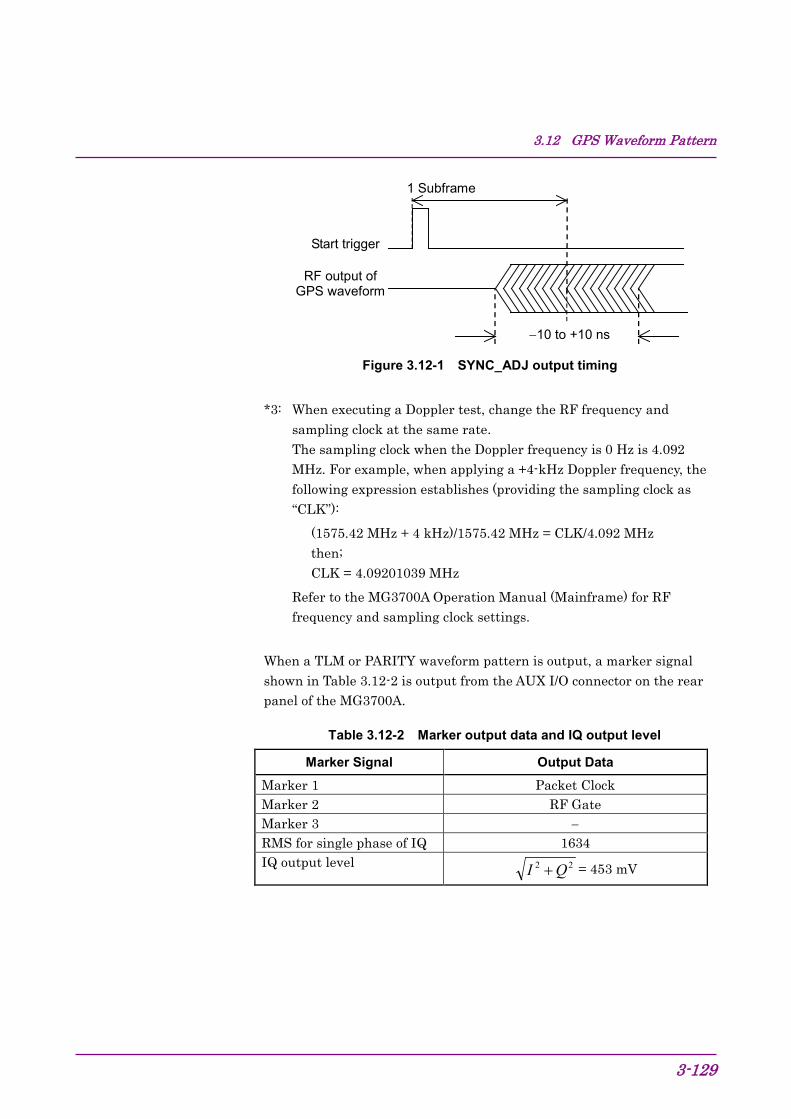
3.12 GPS Waveform Pattern
3-129
RF output ofGPS waveform
−10 to +10 ns
1 Subframe
Start trigger
Figure 3.12-1 SYNC_ADJ output timing
*3: When executing a Doppler test, change the RF frequency and sampling clock at the same rate. The sampling clock when the Doppler frequency is 0 Hz is 4.092 MHz. For example, when applying a +4-kHz Doppler frequency, the following expression establishes (providing the sampling clock as “CLK”):
(1575.42 MHz + 4 kHz)/1575.42 MHz = CLK/4.092 MHz then; CLK = 4.09201039 MHz
Refer to the MG3700A Operation Manual (Mainframe) for RF frequency and sampling clock settings.
When a TLM or PARITY waveform pattern is output, a marker signal shown in Table 3.12-2 is output from the AUX I/O connector on the rear panel of the MG3700A.
Table 3.12-2 Marker output data and IQ output level
Marker Signal Output Data
Marker 1 Packet Clock Marker 2 RF Gate Marker 3 − RMS for single phase of IQ 1634 IQ output level 22 QI + = 453 mV
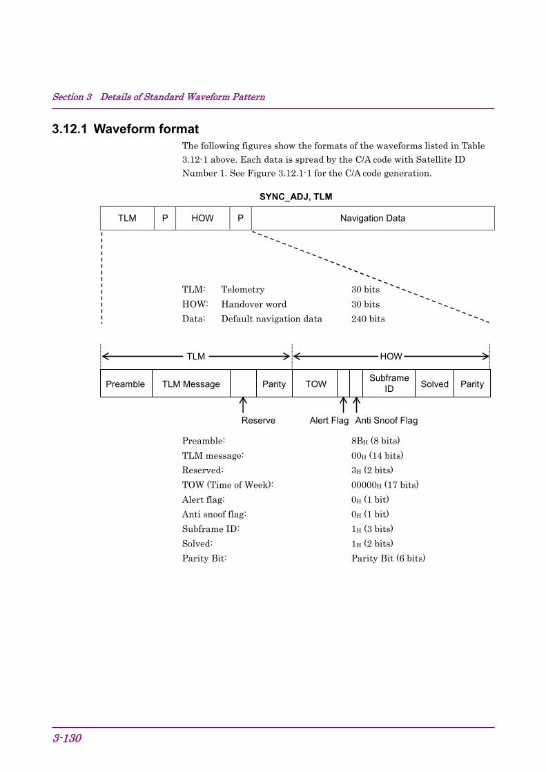
Section 3 Details of Standard Waveform Pattern
3-130
3.12.1 Waveform format The following figures show the formats of the waveforms listed in Table 3.12-1 above. Each data is spread by the C/A code with Satellite ID Number 1. See Figure 3.12.1-1 for the C/A code generation.
SYNC_ADJ, TLM
TLM P HOW P Navigation Data
TLM: Telemetry 30 bits HOW: Handover word 30 bits Data: Default navigation data 240 bits
TLM Message Preamble Parity Parity TOW Subframe
ID Solved
TLM HOW
Reserve Anti Snoof Flag Alert Flag
Preamble: 8BH (8 bits) TLM message: 00H (14 bits) Reserved: 3H (2 bits) TOW (Time of Week): 00000H (17 bits) Alert flag: 0H (1 bit) Anti snoof flag: 0H (1 bit) Subframe ID: 1H (3 bits) Solved: 1H (2 bits) Parity Bit: Parity Bit (6 bits)
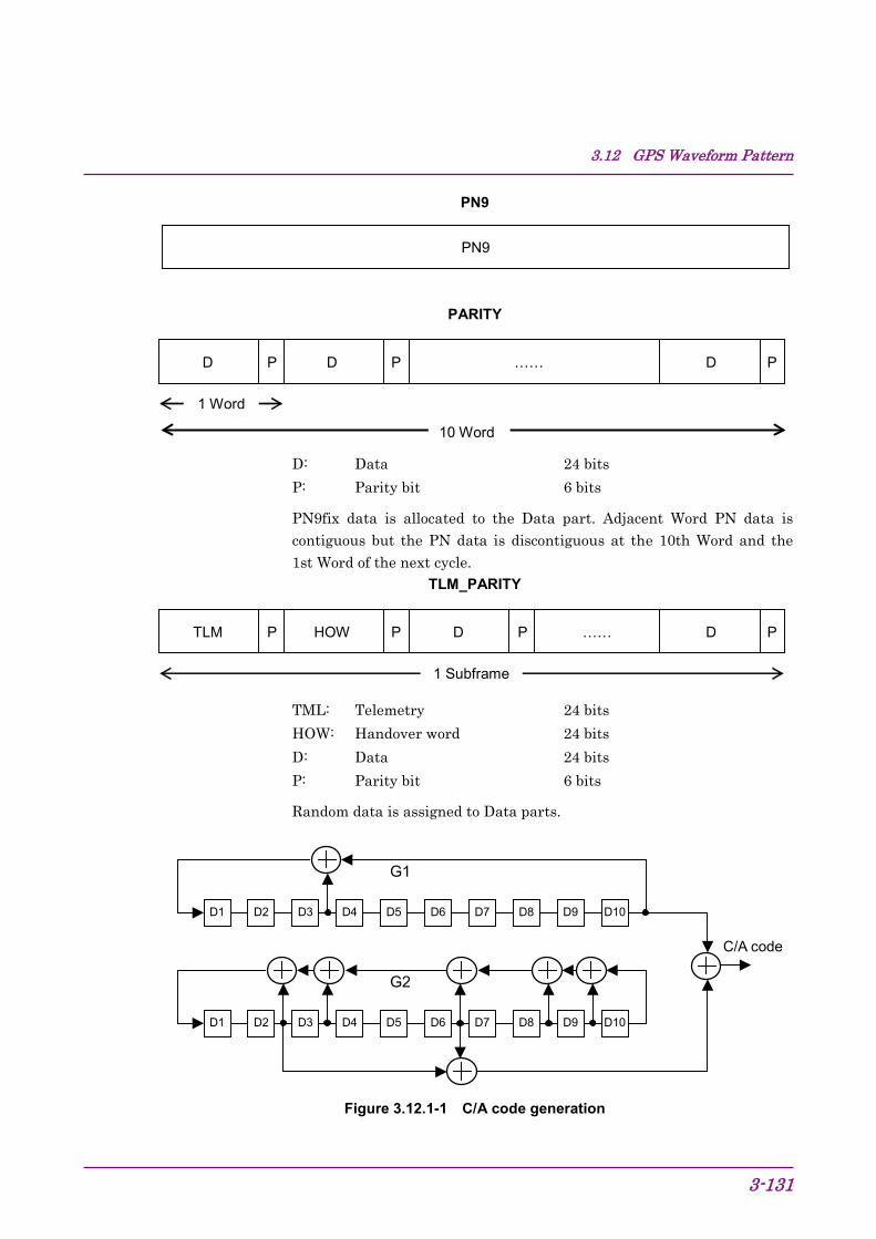
3.12 GPS Waveform Pattern
3-131
PN9
PN9
PARITY
P D
1 Word
P D …… P D
D: Data 24 bits P: Parity bit 6 bits
PN9fix data is allocated to the Data part. Adjacent Word PN data is contiguous but the PN data is discontiguous at the 10th Word and the 1st Word of the next cycle.
TLM_PARITY
P TLM
1 Subframe
P HOW …… P D P D
TML: Telemetry 24 bits HOW: Handover word 24 bits D: Data 24 bits P: Parity bit 6 bits
Random data is assigned to Data parts.
G1
G2
C/A code
D1 D2 D3 D4 D5 D6 D7 D8 D9 D10
D1 D2 D3 D4 D5 D6 D7 D8 D9 D10
Figure 3.12.1-1 C/A code generation
10 Word

Section 3 Details of Standard Waveform Pattern
3-132.
Index
Index-1
Numeric 1xEV-DO forward (excluding FWD_Idle)
3.7.1 1xEV-DO forward idle slot 3.7.3 1xEV-DO reverse 3.7.2 1xRTT Forward RC1, 2 (FWD_RC1-2 9channel)
3.6.7 1xRTT Forward RC3, 4, 5 (FWD_RC3-5 9channel)
3.6.8 1xRTT Reverse RC1 (RVS_RC1_FCH)
3.6.1 1xRTT Reverse RC2 (RVS_RC2_FCH)
3.6.2 1xRTT Reverse RC3 (1) (RVS_RC3_FCH)
3.6.3 1xRTT Reverse RC3 (2) (RVS_RC3_FCH_SCH)
3.6.4 1xRTT Reverse RC3 (3) (RVS_RC3_DCCH)
3.6.5 1xRTT Reverse RC4 (RVS_RC4_FCH)
3.6.6 A AWGN waveform pattern 3.9 B Bluetooth waveform pattern 3.11 C CDMA2000 1X waveform pattern
3.6 CDMA2000 1xEV-DO waveform pattern
3.7 D DL_AMR_TFCSx/DL_ISDN/DL_384kbps_Packet
3.1.5 DL_Interferer 3.1.6 DL_RMCxxxkbps 3.1.4
Digital broadcast waveform pattern 3.10
Details of each GSM waveform pattern 3.5.1
Details of standard waveform pattern Section 3
F Frame configuration 3.2.1, 3.3.1, 3.4.1,
3.5.2 G GPS waveform pattern 3.12 GSM waveform pattern 3.5 H How to use standard waveform pattern
2.1 I IEEE802.11a 3.8.1 IEEE802.11b 3.8.2 IEEE802.11g 3.8.3 O Outline Section 1 Outline of product 1.1 P PDC PACKET waveform pattern
3.3 PDC waveform pattern 3.2 PHS waveform pattern 3.4 S Slot configuration 3.2.2, 3.3.2, 3.4.2,
3.5.3
Index
Index-2.
T TestModel_5_xDPCH 3.1.8 TestModel_5_xHSPDSCH 3.1.9 TestModel_6_xHSPDSCH 3.1.10 TestModel_x_xxDPCH 3.1.7 U UL_AMR_TFCSx/UL_ISDN/UL_384kbps_Packet
3.1.5 UL_AMR_TFCSx/UL_ISDN/UL_64kbps_Packet
3.1.2 UL_Interferer 3.1.3 UL_RMCxxxkbps 3.1.1 W-CDMA waveform pattern 3.1 W-LAN waveform pattern 3.8
Recommended


![Vector Signal Generator MG3710A Product Introduction · Vector Signal Generator MG3710A Features AWGN generator [Opt-049/079] AM/FM/ M/PM Functions [Standard] Additional analog modulation](https://img.pdfslide.us/doc/110x75/5eb581a18015c7750f3b383c/vector-signal-generator-mg3710a-product-introduction-vector-signal-generator-mg3710a.jpg)