AD-A~llb'S CONSTRUCTION ENGINEERIMO RESEARCH LAB (ARMY) CHAMPAIGN IL F/6 13/R7'MICROPROCESSOR CONTROL.LED WELD ARC SPECTRUM ANALYZER FOR GUALIT-EC CU)JUN BA M E MORRIS, C. G ARDNER
UNCLASSIFIED CERL -M317
mEEEIIIEIIE
mEEmhhEEIEEEEE
EI/EBhIE/hEEEE
lEEEEEEE-EEHlllEEEEllllINEEElEEEmlEllllE
construction U M A
engineering S" "Ow "O.s,,, ftoon. TECHNICAL MANUSCRIPT M-317
research NDT Weld Quality Monitor/Semi-Automatic Welding
laboratory
MICROPROCESSOR CONTROLLED WELD ARC SPECTRUMANALYZER FOR QUALITY CONTROL AND ANALYSIS
Michael E. Norris
NN
=Approved for public release; distribution unlimited.
002

The contents of this report are not to be used for advertising, publication, or
promotional purposes. Citation of trade names does not constitute anofficial indorsement or approval of the use of such commercial products.The findings of this report are not to be construed as an official Department
of the Army position, unless so designated by other authorized documents.
DESTROY THIS REPORT WHEN IT IS NO LONGER NEEDEDDO NOT RETURN IT TO THE ORIGIN4 TOR

UNCLASS I FI EDSECURITY CLASSIFICATION OF THIS PAGE (When Dete Entered)
READ INSTRUCTIONSREPORT DOCUMENTATION PAGE BEFRE_ COMPLETINGORM
1. REPORT NUMBER GOVT ACCESSION NO. 3. RECIPIENT'S CATALOG NUMBER
CERL-TM-M-317 A-).9// r /4. TITLE (mtd Subtitle) 5. TYPE OF REPORT & PERIOD COVERED
MICROPROCESSOR CONTROLLED WELD ARC SPECTRUM
ANALYZER FOR QUALITY CONTROL AND ANALYSIS FINAL
6. PERFORMING ORG. REPORT NUMBER
7. AUTHOR(.) S. CONTRACT OR GRANT NUMBER(&)
M.\ E. NORRIS
C. S. GARDNER
3. PERFORMING ORGANIZATION NAME AND ADDRESS 10. PROGRAM ELEMENT. PROJECT. TASKU.S. ARMY AREA & WORK UNIT NUMBERS
CONSTRUCI ON ENC I NEER [N( RESEARCH LABORATORY 4A76273]AT4I-C-(J3(P.O. BOX 4005, CHAMPAIGN, [.L 61820
II. CONTROLLING OFFICE NAME AND ADDRESS 12. REPORT DATE
June 198213. NUMBER OF PAGES
13614. MONITORING AGENCY NAME & AODRESS(If different from Controlling Office) IS. SECURITY CLASS. (of this report)
1Sa. DECLASSI FICATION/DOWNGRADINGSCHEDULE
16. DISTRIBUTION STATEMENT (of thls Report)
Approved for public release; distribution unlimited.
17. DISTRIBUTION STATEMENT (of the abstract entered In Blok 20, If different from Report)
IS. SUPPLEMENTARY NOTES
Copies are obtainable from the National Technical Information Service
Springfield, VA 22151
SI9. KEY WORDS (Continue on revere. side Ii neceaaory nd Identify by block number)
Welded joints
nondestructive testing
spectrographsmicroprocessors
2&} ABISTRACT' (Cetfime - ,eversm e Fi n.eoes end Idenity by block number)
,This thesis describes the components and operation of a system designed toanalyze parameters associated with a weld arc. In particular, the spectrum,
voltage, current, and travel speed of the weld arc are sampled by a micro-processor For anatysts.
DOA"3 I0,A, EDITIO m Of IF NOV 6S S OLETIEI JAN~I 1473 EUNCLASSIFIED
SECURITY CLASSIFICATION OF THIS PAGE (When Date Entered)

UNCLASS 1 FT EDSECURITY CLAIIFICATION OF THIS PAGE(Phu, Data Ete'.0
BLOCK 20 Continued
The system is broken down into hardware and software components, whichare described in detail, and an operating procedure for the system is provided.Experimental results are given which correlate changes in the weld parameterswith the occurrence of defects. Changes in the voltage and current of the arcare correlated with spectral changes of the arc. A correlation between thespectral energy and weld heat input is also presented.
UNCLASSIFIED
SECURITY CLASSIFICATION OF THIS PAGE(yi n Dom Entered)

FOREWORD
This research was conducted in partial fulfillment of the requirements
for the degree of Master of Science in Electrical Engineering at the
University of Illinois at Urbana-Champaign. The work was conducted at the
University of Illinois, Radio Research Lab (RRL). The work was funded by
the U.S. Army Construction Engineering Research Laboratory (CERL) under
Project 4A762731AT41, "Military Facilities Engineering Technology,"
Technical Area B, "Construction Management and Technology," and Work Unit
030, "NDT Weld Quality Monitor/Semi-Automatic Welding." COL Louis J. Circeo
is Commander and Director of CERL, and Dr. L. R. Shaffer is Technicl
Director.
I would like to thank Dr. C. S. Gardner for his guidance and assistance
in my pursuit of a Master of Science. I would also like to thank Frank Kearney
of CERL, whose advice was instrumental in completing this project and
Rich Davis, a fellow graduate student, for his assistance in compiling data.
.NTTS v.".3.I C
J. c
. . . . . . I - I . . . l . .. . . . .. . l~ . . I . . . . . ,i . . . . . ._3, L -

TABLE OF CONTENTS
DD FORM 1473FOREWORDLIST OF TABLESLIST OF FIGURES
Chapter Page
1. INTRODUCTION .. .... ...................... 11
2. AN OVERVIEW OF THE WELD QUALITY MONITOR SYSTEM .. .. ....... 14
3. THE WELD QUALITY MONITOR SYSTEM. .... ............ 15
3.1 Spectrograph and Fiber Optics .. ........ ...... 15
3.1.1 Fiber optic bundle .. .... ............ 153.1.2 Spectrograph .. ..... .............. 15
3.2 Photodiode Array and Electronics .. ............. 183.3 LSI-11 Hardware Description .. .... ........... 23
3.3.1 11/23 Cen1iral Processing Unit (CPU) description . 23*I3.3.2 Input/output description .. .... ......... 23
3.3.2.1 Serial interfarte description .. ....... 233.3.2.2 Parallel interface description .. ...... 26
3.3.3 Floppy disk description .. .............. 323.3.4 Analog to digital converter .. ............ 343.3.5 Direct Memory Access description. .. ......... 39
3.4 LSI-11 Software Description for the WQM. .. ......... 41
3.4.1 Fortran program. .... .............. 413.4.2 Macro program. ... ................. 50
4. OPERATING PROCEDURE. ..... .................. 62
5. EXPERIMENTAL RESULTS. .. ..................... 75
6. CONCLUSIONS. ....... .................... 92
APPENDIX A. SPECIFICATIONS AND SCHEMATICS ON RETICON DIODEARRAY AND SCANNING ELECTRONICS .. ............ 93
APPENDIX B. SCHEMATICS AND CALIBRATION PROCEDURE FOR THEADAC 1012 A/D CONVERTER. .. ............... 99
APPENDIX C. SCHEMATICS FOR THE ADAC 1620 D44.. ........... 105
APPENDIX 0. THE MACRO PROGRAM FOR THE WQM. .. ............ 111
4
APPENDIX E. THE FORTRAN PROGRAM FOR THE WQM. .............. 115
APPENDIX F. AN EXAMPLE OF THE DATA OBTAINED FROM THE WQM WHENDISPLAYED ON THE DECV7.iTLA LA-120. ............... 127
APPENDIX G. AN EXAMPLE OF CALIBRATION DATA FOR THE SPECTROGRAPHTAKEN USING THE WQM ..................... 131
APPENDIX H. FLOPPY DISK INITIALIZATION AND FORMATTING .. ........ 135
REFERENCES................................136
DISTRIBUTION
5

LIST OF TABLES
TABLE Page
1. RESOLUTION OF SPECTROGRAPH. ... ............... 15
2. BAUD RATE JUMPERS [5] .. ......... ........... 25
3. CHANNEL ADDRESSES FOR SERIAL I/O BOARD [6] .. .......... 28
4. INTERFACE PIN ASSIGNMENTS FOR PARALLEL I/O BOARD [7] .. .... 29
5. ADDRESSING STRUCTURE FOR PARALLEL I/O BOARD .. .... ..... 29
6. DEVICE ADDRESS JUMPERS FOR PARALLEL 1/O BOARD 171. .. .. ... 30
7. INTERRUPT VECTOR ADDRESS JUMERS FOR PARALLEL I/OBOARD 171 .. .. ... .... .... .... ..... ..... 30
8. ADDRESSING STRUCTURE OF DMA .. .. ............... 40
9. CONVERSION FACTORS. .... .................. 51
6
LIST OF FIGURES
Figure Pige
1. Block diagram of microprocessor controlledspectrograph ......... ....................... ... 12
2. Fiber optic bundle to spectrograph .... ............ ... 16
3 Transmittance curve for fiber bjundle ... ........... ... 16
4a. Spectrograph (top view) ......... .................. 17
4b. Spectrograph ......... ....................... ... 17
5. Photodiode array ........ ..................... ... 19
6. Optical response of photodiode array ... ........... ... 20
7. Start pulses ......... ....................... ... 21
8. Video output ......... ....................... ... 21
9. Clock pulses ......... ....................... ... 21
10. Spectrum with Helium-Neon laser ..... .............. ... 22
11. Expansion of spectra showing individual diode levels . 22
12. Synchronization circuitry ...... ................. ... 24
13. Timing diagram for synchronization .... ............ . 24
14. Jumper locations on serial I/O board [6] .. ......... .. 27
15. Jumper locations on DRVl-C [7]. ..... .............. .. 31
16. RXV21 floppy disk board ....... .................. ... 33
17. RX02 floppy disk drive ....... .................. ... 33
18. Jumper and adjustment locations on A/D [9]. ........... .35
19. Jumper switches for addressing for 1012 A/D ........... .. 37
20. Pin assignments for I/O on ADAC 1012 A/D .. ......... .. 37
21. Flowchart of FORTRAN program ..... ............... .. 43
22. User Flowchart of FORTRAN program ..... ............. 47
23. Flowchart of macro program ...... ................ ... 53
7

Figure Page
24. Back view of WQM ........ ..................... .. 63
25. Backplane of DEC minicomputer ..... .............. .64
26. Back of spectrograph control box .... ............. .. 64
27. Decwriter LA-120 ........ ..................... .. 65
28. Front of spectrograph control box .... ............. .67
29. Front of DEC minicomputer ...... ................. .67
30. Front of WQM. ......... ....................... .68
31. Keyboard for Decwriter LA-120 [10] .... ............ .. 70
32. Weld spot and fiber ........ .................... .76
33. Variation of the arc voltage and current versus time . . . 77
34a. Spectrum obtained at 28.71 seconds into the experimentand corresponds to normal welding conditions where theargon shielding gas is on ...... ................. .79
34b. Spectrum obtained at 29.7 seconds into the experimentand corresponds to abnormal welding conditions whenthe shielding gas is off ................. 79
35. Total energy in the spectral segment from 700 to 1000nanometers .......... ........................ .80
36. Total energy in the spectral segment from 400 to 700nanometers .......... ........................ .82
37. Total energy in the spectral segment from 400 to 1000nanometers ................................... 83
38. Total energy in the spectral segment from 814 to 816nanometers .......... ........................ .85
39a. Normal argon shielded weld ...... ................ .86
39b. Weld made without shielding gas ..... .............. ... 86
40. Variation of the arc voltage and current versus time . . . 87
41. Variation of the total energy in the spectral segmentfrom 400 to 1000 nm versus eat input .... ............ 86
8

Figure Page
42 Variation of the total energy in the spectral segment
from 400 to 700 nm versus heat input ... ........... .. 89
43 Variation of the total energy in the spectral segment
from 700 to 1000 nm versus heat input ... .......... .90
9

1. INTRODUCTION
During the welding process, changes in arc voltage, travel speed,
heat input and shielding gas content can cause defects which seriously de-
crease the service life of the welded joint. The cost of locating and
repairing these defects can be a major portion of the construction costs.
During the past decade, the Construction Engineering Research Laboratory (CFRL)
has been developing a real-time weld quality monitor to detect flaws as they
occur [1] - [3]. Recent work at CERL has indicated that it may be possible
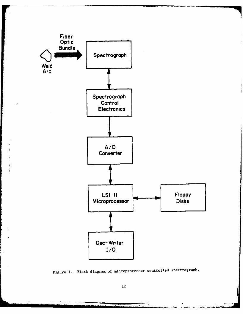
to detect weld flaws using electrooptical techniques. This paper describes
a microprocessor controlled spectrograph for use with the CERL weld quality
monitor.
Construction Engineering Research Laboratory engineers developed a
low-resolution arc spectrum analyzer [2]. Photographic filters were used
to divide the arc spectrum into five bands spanning the range from 400 to
1000 nanometers. With this device it was possible to separate and quantify
segments of the weld spectrum and correlate the energy distribution among
these segments to specific weld parameters. The results indicate that it
may be possible to classify weld flaws based upon the energy distribution
in the arc spectrum.
To supplement and extend this work, a high-resolution microprocessor-
controlled spectrograph was developed. A block diagram of the system is
illustrated in Figure 1. The optical radiation emitted by tbt weld arc in
the region from 300 to 1200 nanometers is collected by a fiber optic bundle.
The bundle, which is designed to withstand the higher temperatures surrounding
the weld arc, is terminated at the spectrograph entrance slit. The light
passing through the slit is reflected by a mirror to a concave holographic
11
FiberOptic
( B d Spectrograph
WeldArc
SpectrographControl
Electronics
AIDConverter
LSI-11FlppMicroprocessor Disks
Dec- WriterI/O
Figure 1. Block diagram of microprocessor controlled spectrograph.
12

grating which images the spectral range from 300 to 1200 nanometers onto a
1024 element linear photodiode array. The spectrograph resolution is on
the order of 1 nanometer. The photodiode array is interfaced to a high-
speed analog-to-digital converter and LSI 11/23 microprocessor. The spectral
data along with measurements of the arc voltage, vrrent, and travel speed
can be processed or stored on floppy disks for later analysis.
With this system, important features of the weld arc can be observed in
real time and correlated with weld flaws. This report describes in detail
the system design and operation.
13
__ _ __ _ _ _ S

2. AN OVERVIEW OF THE WELD QUALITY MONITOR SYSTEM
The Weld Quality Monitor (WQM) is comprised of three parts: the
optical and electronic hardware to measure the weld arc spectrum, the
Digital Equipment Corporation (DEC) LSI-11 microcomputer for data
acquisition and storage, and the software to control the WQM. The optical
hardware is composed of a lens and fiber optic bundle that gathers the
optical radiation from the weld and guides it to the spectrograph. The
spectrograph uses a holographic grating to image the spectrum on a photo-
diode array that is controlled by scanning and synchronization circuitry.
Data are acquired by an analog-to-digital (A/D) converter that is controlled
by Direct Memory Access (DMA) electronics. The user interface, data transfer,
and WQM control are maintained by either Fortran IV or the DEC machine
language, Macro-ll. The device initialization, synchronization, and data
acquisition programs are written in Macro-ll. The user interface programs
that are necessary for data specification and display are written in
Fortran IV.
14
L~ ~ ~ ~ ~ ~ ~ ~ ~~~~~~~~~~~---- --...... ,LL i ...... '.. ..... "" ''" - " "

3. THE WELD QUALITY MONITOR SYSTEM
3.1 Spectrpraph and Fiber Optics
3.1.1 Fiber optic bundle
The Dolan-Jenner fiber optic bundle is a steel clad industrial cable ca-
pable of withstandiag 260 degrees centigrade (500 degrees Fahrenheit) temper-
atures (see Figure 2). It has an acceptance cone of 68 degrees and a numerical
aperture of 0.55. Figure 3 [4] shows the transmittance curve for different
lengths of cable. It is easily seen that the ultraviolet and middle infrared
regions are severely attenuated. Fortunately, due to the high intensity of
radiation emitted from the weld arc, signal strength can compensate for some
of the losses.
3.1.2 Spectrograph
The spectrographs shown in Figures 4a and 4b have three different slit
widths of 50, 100, and 250 pm. Light passes from the fiber bundle through
the slit and strikes an ISA holographic grating. Either a 200-1200 nm or
200-800 nm range grating may be used. Using these slit widths and gratings
produces the variation in resolution shown in Table 1. These are somewhat
idealized results in that they neglect spillover into other diodes, parallax
in alignment, and defocusing errors. Actual resolution may be as much as one
nanometer worse than the values given.
TABLE 1
RESOLUTION OF SPECTROGRAPH
SlitWidths 50 Pm 100 Pm 250 pm
Grating i
200-1200 nm 1.95 nm 3.91 nm 9.76 nm
400-900 nm 1.17 nm 2.34 nm 5.86 nm
15

f iberopticbundle
Figure 2. Fiber optic bundle to spectrograph.
TYPE X GLASS FIBER OPTIC TRANSMITTANCE
Fresnel Reflection 5.6 % / SurfaceCore/Clad Ratio 82%Packing Fraction 83%
100-
U 80-
~z 60-3(.9)
cc 4 0 -
WAVL0 GT (jsm)
Figure 3. Transmittance curve for fiber bundle.
16
WON----______
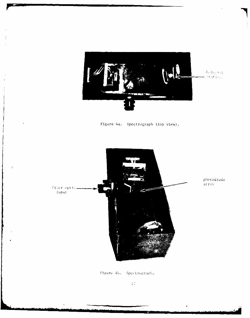
Figure 4a. Spectrograph (top view).
p1 I0 LU dV d
lput
Figutre 41). Spcr L ro~iraphli

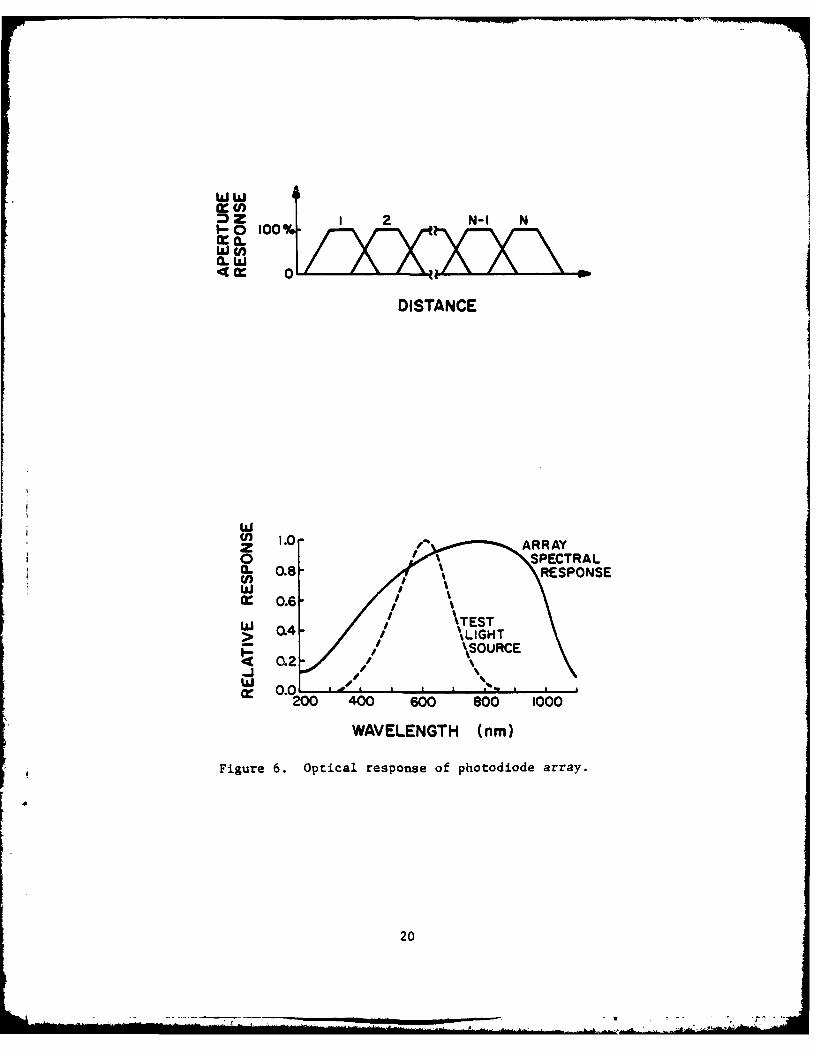
3.2 Photodiode Array and Electronics
The optical sehsor consists of a 1.008-inch linear array of 1024 silicon
photodiodes, 15 pm high, and 25 m spacing. These dimensions are illustrated
in Figure 5. Spectral responsivity, governed by the quartz window covering
the array, the aperture response, and the quantum nature of the diodes them-
selves, decreases to about 20% at 250 and 1000 nm (see Figure 6).
Each diode has a storage capacitor for integration of the photo current.
The charge on the storage capacitor is gradually removed by the reverse
current generated by the photodiodes. Each capacitor is sequentially sampled
by multiplex switches turned on and off by a shift register driven by a two-
phase clock. At the end of each sample, the capacitor is recharged to +5 V.
The clock sequence is initiated by a start pulse (see Figure 7).
The support electronics consist of sample and hold circuitry. The video
line is set to ground prior to each diode sample. When a multiplex switch is
closed, charge is divided between the photodiodes and the video line. This
line is sapled and held, giving the display shown in Figure 8. The start
pulse and clock (see Figure 9) are set by the user. Further details on this
and other aspects of the array are contained in Appendix A.
Figures 10 and 11 show the oscilloscope displays of the spectral output
of the electronics box in response to a Helium-Neon laser. Figure 10 shows
the spectrum from 200 to 1200 nm. The wavelength of the radiation from a
Helium-Neon laser is 632.8 nm. The display in Figure 10 verifies this.
Figure 11 is an expanded display of the spectral line of the Helium-Neon laser.
It shows that approximately three diodes are illuminated by the laser
radiation. This corresponds to about 3 nm, which is as might be expected
using the 50-micrometer slit on the spectrograph.
18
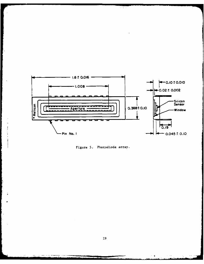
1.6t 0.016
1.008 01 .1
r-0.02 ± 0.002
-Sicon
0.388± 0.10",.-Window
Pin o. 10.045± 0.10
Figure 5. Phoodiode array.
19
........
ww
Wy
DISTANCE
Wl1.0.f2 SPECTRAL
IL 0.8- RESPONSEM 0 .6 - 0 R A
IIH20%S

LH H36ALs
Figure 7. Start pulses.
Figure 8. Video output.
4 37/As4Vt
-- 47ms
Figure 9. Clock pulses.
21

Figure 10. Spectrum with Helium-Neon laser.
F igure 11. Expansion of -;p(('t r;l ShIowing inldividuLV diode levels.
22 ~

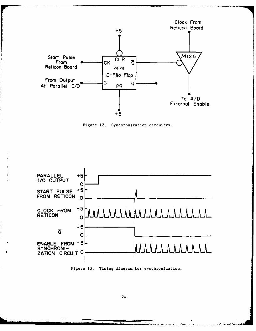
The scanning electronics for the diode array run continuously. Thus,
in order for the A/D to sample the diode levels accurately, synchronization
circuitry must be provided, which is illustrated in Figure 12. The start
pulse used to initiate the video scan sets a D flip flop. The D flip flop
in turn opens a gate that allows the same clock pulses to be used by the
A/D as an external enable. Thus the A/D is triggered synchronously with
the video line out. The DMA has a word counter that is preset to 1024 so
that sampling is terminated after all 1024 photodiodes are sampled. Figure
13 gives a timing diagram of the sequence of events.
3.3 LSI-11 Hardware Description
3.3.1 11/23 Central Processing Unit (CPU) description
The Digital Equipment Corporation (DEC) LSI 11/23 is a 16-bit word
or 8-bit byte-oriented microprocessor. It is capable of executing over
400 machine language instructions. With the proper system software, it
is further capable of handling Fortran, Pascal, APL, and Basic. The machine
language utilized (Macro-ll) is a stack-oriented language with eight general-
purpose registers. Without extended software this language will directly
access 64K words of memory. The lower 376 locations are reserved for
interrupt vectors and traps. The top 8K works are reserved for peripheral
device addressing. Further details on both the hardware and software
associated with the 11/23 can he found in the DEC Microcomputer Processor
Handbook [41.
3.3.2 Input/output description
3.3.2.1 Serial interface description. The serial interface for the
LSI 11/23 is a DEC DLVll-J. It has four independent full duplex asynchronous
channels capable of 150 to 9600 baud. Table 2 [5] indicates the jumper
23
Clock From+5 Reticon Board
Start PulseFrom - - CK
Reticon Board 7474D-Flip Flop
From OutputAt Parallel I/O 1 PR
To A/D
External Enable
+5
Figure 12. Synchronization circuitry.
PARALLEL +5I/0 OUTPUT 0
START PULSE + 5
FROM RETICON 0
CLOCK FROM + 5
RETICON 0
+5
ENABLE FROM +5-SYNCHRONi-ZATION CIRCUIT 0
Figure 13. Timing diagram for synchronization.
24
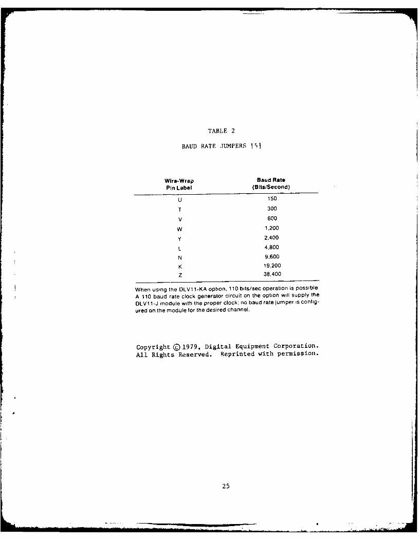
TABLE 2
BAUD RATE JUMPERS 5V1
Wire-Wrap Baud RatePin Label (Bits/Second)
U 150
T 300
V 600
W 1,200
Y 2.400
L 4,800
N 9,600
K 19,200
Z 38,400
When using the DLVI1-KA option, 110 bits/sec operation is possible.
A 110 baud rate clock generator circuit on the option will supply the
DLV11-J module with the proper clock; no baud rate jumper is config-
ured on the module for the desired channel.
Copyright ©1979, Digital Equipment Corporation.All Rights Reserved. Reprinted with permission.
25
selections made on the DLVl1-J to select the desired baud rate. Figure 14 [6]
shows the location of the jumpers on the board.
Each channel is composed of a receiver control status register (RCSR),
rcceiver buffer (RBUF), transmitter control status register (XCSR), and
transmitter buffer (XBUF). The factory jumpered addresses for these
channels are shown in Table 3 [6]. Further information on the DEC DLV11-J
can be obtained in the DEC Microcomputer Interfaces Handbook, pp. 221-
249 [6].
3.3.2.2 Parallel interface description. The parallel interface is
an MDB MLSI-DRVll-C. It has sixteen TTL and DTL logic compatible input and
output lines with four control lines for a peripheral device: NEW DATA READ,
DATA TRANSMITTED, REQUEST A, and REQUEST B. Tables 4 [7] and 5 show the inter-
face pin assignments and the addressing structure, respectively. Device
address locations can be changed 1y utilizing the jumper selections shown in
Table 6 [7]. Table 7 [7] shows the jumpers for selection of Interrupt
Vectors. Figure 15 [7] shows the location of the jumpers on the module.
The Control Status Register (CSR) is a 16-bit word that is used to
control the parallel I/0 board. The bits in the CSR have the following
functions:
BIT NAME DESCRIPTION
15 REQUEST B A read only bit that is cleared by systeminitialization. This bit is set by a periph-eral device and may be used as a flag for
device status. It may also be used as aninterrupt request if bit 5 is also set.
14-8 Unused
7 REQUEST A It has the same function as REQUEST B except the
interrupt is generated only if bit 6 is set.
26

CHO AND MOJ M2 CH2 ANDSCION O MI. r-~ &[ 0-0 .-. CH3 EIA
SELCTIN M1 0--NO - : R2 * .0 3 SELECTION
0H~ B0 AUD RATECH 1 102 : SELECTION
P 0 0 -4
PeCHIrEr ol CI TERM RESISTORCHI) Do L-4CHO TERM RESISTOR
COMMUNICATION si-'&,CH2 TERM RESISTORLINE P CHM2* CH3 TERM RESISTOR
PARAMETERS E C-0-
CH2 Do4-.P.0.-0
CH3E S
CH3 S 4-W- ADDRESS ANDP 0 *-- VECTOR JUMPERS
A5 47ilA9-01
A12o A6 0-AlOe *._7Allo o-o Ao-
A4 7-
Figure 14. Jumper locations on serial 1/0 board [6].
Copyright@©1981, Digital Equipment Corporation.All Rights Reserved. Reprinted with permission.
27

TABLE 3
CHANNEL ADDRESSES FOR SERIAL 1/O BOARD [61
Address Register Vector
176500 RCSN176502 RBUF 300176504 XCSR Channel 0176506 XBUF 304
176510 RCSR176512 RBUF 310176514 XCSR Channell176516 XBUF 314
* I176520 RCSR176522 RBUF 320
*176524 XCSR Channel 2176526 XBUF 324
177560 RCSR177562 RBUF 60177564 XCSR Channel 3177566 XBUF 64
Copyright © 1981, Digital Equipment Corporation.All Rights Reserved. Reprinted with permission.
28

TABLE 4
INTERFACE PIN ASSIGNMENTS FOR PARALLEL I/0 BOARD [7]
it J2
Signal Pin Signal Pin
OUT00 C IN N00 TT
OUT0! K IN01 ILLOUT02 NN. RR IN02[ H. EOU T03 u iN03 BBOUT04 L IN04 KKOUT05 N IN05 H HOUT06 R IN06 EEOUT07 T IN07 CCOUT08 W IN08 ZOUT09 X IN09 YOUTIO Z INIO %VOUTI I AA INt kOUTI2 BB IN12 uOUT13 FF IN13 POUTI4 HH IN14 NOUT15 Ji IN15 MINIT P INIT RR. NNNEW DATA READY VV DATA TRANSMITTED CCSRI DD CSRO KREQUEST A LL REQUEST B SGXD J. M, S, GND J, L. R.
V. cc. T. X. AA.FF. KK. DD, JJ,MM. PP. %IM. PP.SS. UU SS. UL
TABLE 5
ADDRESSING STRUCTURE FOR PARALLEL I/O BOARD
Address Name Mnemonic Address
Control Status CSR 167770Register
Output Buffer OUTBUF 167772
Input Buffer INBUF 167774
*f 29

TABLE 6
DEVICE ADDRESS JUMPERS FOR PARALLEL 1/O BOARD [7]
Address Jumper Connect ConnectBit Location for "I" for "0r
12 4 K-i H-i11 5 N-M L-M10 5 H-i K-i09 3 N-M L-M08 2 L-M N-M07 1 H-i K-i06 4 L-M N-M05 3 K-i H-i04 2 H-i K-i03 1 L-M N-M02 Bits 00, 01, and 02 are hardwired01 and pro~ramn-cont rolled.00 __ _ _ _ _ _ _ _
TABLE 7
INTERRUPT VECTOR ADDRESS JUMPERS FOR PARALLEL 1/O BOARD [7]
Address Jumper Connect OmitBit Location for "0" for '"
07 6 H-i H-i06 8 H-i H-i05 9 H-i H-i04 10 H-i H-i03 7 H-i H-i02 none hardwired
30

o 0J2
JFJ~IJ
F U ~EI~ EJ4L3~E
EQ ~~ l~~Diii L LI fl
DL
M
B-B_
Figure 15. Jumper locations on DRV11-C [7].
31
BIT NAME DESCRIPTION
6 ENTENBA A read/write bit cleared by system initialization.When set, it will enable an interrupt to occurupon the setting of bit 7.
5 INTENBB It has the same function as bit 6 except it appliesto bit 15. Cleared by system initialization.
4-2 Unused
1 CSR 1 A read/write bit cleared by system initialization.It can be used to flag a device.
0 CSR 0 Same as bit 1.
More information can be obtained from the MDB MLSI-DRV11C Parallel Line
Interface Module Instruction Manual [6].
The DRVlIC is used to synchronize the A/D converter with the video
line from the Reticon scanning electronics. By moving a 1 into the output
buffer, pin C is set on the output cable. This line is then tied to the
input of a D flip flop that opens a gate at the occurrence of a start signal
from the array scanning electronics that initiate scanning. When the gate
opens, it allows the video clock signal to trigger the A/D converter.
3.3.3 Floppy disk description
The floppy disk control module is a DEC RXV21 (see Figure 16) board
that controls a dual density RX02 floppy disk drive (see Figure 17). Each
floppy disk is capable of storing 512,512 eight-bit bytes per diskette.
The average access time (composed of seek, settle, and rotate time) is
262 msec. Additional details on the operation of the RXV21 with the RX02
drive can be found in the DEC Microcomputer Interfaces Handbook, pp. 608-
628 [6].
Floppy disk files can be accessed for reading or writing either manually
or under program control. The system provides two methods for user inter-
active editing of disk files. The RT-l1 editor provides a simple but
32

Figure 16. RXV21 floppy' disk board.
* ri
V ue17. RXO) fIlppx' d isk dr i v,

unsophisticated means for editing disk files. An easy-to-read, step-by-step
introduction is provided in volume lB, "Introduction to RT-ll," Chapter 5,
"Creating and Editing Text Files," of the RT-11 Operator Manuals [8]. A
more sophisticated method of editing files is provided by using TECO (Text
Editor and Corrector). Unlike the RT-11 editor, TECO is character-oriented
rather than line. Thus, it provides the user with better scanning software.
A complete guide to TECO is provided in the "TECO Users Guide," volume 2
of the RT-11 Operator Manuals [8].
There are three other methods of writing arnd reading files on floppy
disks. The crudest of these three is done using macros. It has, however,
the advantage of using less space for program storage and of being faster.
Chapter 2 of the "Advanced Programmer's Guide," volume 3 of the RT-11
Operator Manuals [8], describes the program requests available. The other
two methods are accessed as RT-11 Fortran subroutines. Unfortunately, in
order to understand the subroutine available, a good understanding of the
macro program request is essential. The Fortran system subroutine libraryIcontains the necessary routines needed to allocate channels, name devices, etc.
A combination of all these subroutines is contained in two subroutines called
OPEN and ASSIGN. They are very sophisticated ard require a good understanding
of the Fortran system subroutines from which they are built. A description
of these two commands can be found in Appendix B of the "Fortran User's
Guide," volume 4 of the RT-l.l Operator Manuals [8].
3.3.4 Analog to digital converter
The AID converter is an ADAC Model 1012 (see Figure 18) [9]. It has
16 single-ended, pseudo difference, or differential inputs. Each line has
programmable gain, 100 KHz throughput (10 microsecond settling and conversion
34

V 1II1 T I
Figure 18. Tumper and adjust;,ient locations on A/I) [9].
35
time), and 12-bit resolution. Nine optional hard jumpered features on the
A/D are the input range, type of input configuration, trigger, status register,
external enable, vector, external trigger, DMA, and external power. All of
these jumpered options are discussed in the ADAC Instruction Manuals,
pp. 27-28 [9]. Presently, the board is configured for a -10 to +10 voltage
input range, single-ended input, external triggering, bit 1 as the external
enable in the CSR, DMA control disabled (so triggering is done externally),
and no external power.
Switch jumpers are provided for selection of the control status register
and vector interrupt location. These switches are set up as illustrated in
Figure 19 with an off setting as a one and an on setting as a zero. The
current control status register and vector address are 177000 and 130,
respectively.
Input and output are done over a 20 conductor shielded ribbon cable.
Pin assignments for the ribbon cable's connector are given in Figure 20.
Currently, channel 0 is used for the video signal, channel 1 for the voltage,
channel 2 for the current, and channel 3 for the travel speed. The external
trigger is supplied by the synchronization circuitry and Reticon electronics.
Further details on cabling can be found in the ADAC Instruction Manuals,
pp. 14-15 [9].
Control of the A/D is maintained through the status register. It is
set up as follows:
36

I ON D7 1 OFF D12 1 ON D7
2 ON D6 2 OFF DI 2 OFF D6
3 ON D5 3 OFF D1O 3 ON D5
4 ON D4 4 OFF D9 4 OFF D4
5 ON D3 5 ON D8 5 OFF D3
6 ON D2
Si S2 S3
ADDRESS SWITCHES VECTOR SWITCH
Figure 19. Jumper switches for addressing for 1012 A/D.
CANON 3M CANON 3M
PIN PIN PIN PINNUMBER NUMBER NUMBER NUMBER
1 1 CHO-OA IN 20 2 CH8-OB IN
2 3 CHI-lA 19 4 CH9-1B
3 5 CH2-2A 18 6 CHIO-2B
4 7 CH3-3A 17 8 CH11-3B
5 9 CH4-4A 16 10 CH12-4B
6 11 CH5-5A 15 12 CH13-5B
7 13 CH6-6A 14 14 CH14-6B
8 15 CH7-7A 13 16 CH15-7B
9 17 EXT TRIG IN 12 19 POWER RETURN
10 19 AMP LO IN 11 20 SIGNAL RETURN
Figure 20. Pin assignments for I/O on ADAC 1012 A/D.
37
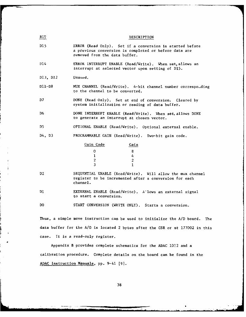
BIT DESCRIPTION
DIS ERROR (Read Only). Set if a conversion is started beforea previous conversion is completed or before data areremoved from the data buffer.
D14 ERROR INTERRUPT ENABLE (Read/Write). When set, allows aninterrupt at selected vector upon setting of D15.
D13, D12 Unused.
Dll-D8 MUX CHANNEL (Read/Write). 4-bit channel number correspo,,dingto the channel to be converted.
D7 DONE (Read Only). Set at end of conversion. Cleared bysystem initialization or reading of data buffer.
D6 DONE INTERRUPT ENABLE (Read/Write). When set, allows DONEto generate an interrupt at chosen vector.
D5 OPTIONAL ENABLE (Read/Write). Optional external enable.
D4, D3 PROGRAMMABLE GAIN (Read/Write). Two-bit gain code.
Gain Code Gain
0 81 42 23 1
D2 SEQUENTIAL ENABLE (Read/Write). Will allow the mux channelregister to be incremented after a conversion for eachchannel.
Dl EXTERNAL ENABLE (Read/Write). A'lows an external signalto start a conversion.
DO START CONVERSION (WRITE ONLY). Starts a conversion.
Thus, a simple move instruction can be used to initialize the A/D board. The
data buffer for the A/D is located 2 bytes after the CSR or at 177002 in this
case. It is a read-only register.
Appendix B provides complete schematics for the ADAC 1012 and a
calibration procedure. Complete details on the board can be found in the
ADAC Instruction Manuals, pp. 9-41 [9].
38

3.3.5 Direct Memory Access description
The ADAC Model 1620 Direct Memory Access (DMA) is a DEC compatible board
that provides a means of transferring digitized data directly from the
ADAC A/D to memory, without CPU intervention. It has an 18-bit memory
address counter, a 6-bit final channel register and comparator, a 16-bit
word counter, and interrupt enable capability. The DMA is composed of four
registers which are described as follows (addressing is described in Table 8):
1) Bus Address Register (BAR): an 18-bit read/write register that
is loaded under program control. The BAR is incremented by
two after each DMA transfer. This address is used to specify
the address in memory to which the data are to be moved. It is
word addressable only.
2) Word Count Register (WC): a 16-bit read/write register that
contains the 2's complement of the total number of cycles to
be completed before DMA termination. It is also loaded under
program control. WC is incremented after each DMA transfer,
and upon overflow, resets READY FF in the Control Status
Register and causes an interrupt request. It is word
addressable only.
3) Multiplex Comparator Register (MCR): a six-bit write only
register that is loaded under program control. It is used
for last channel addressing when used in conjunction with the
1012 A/D. It is word addressable only.
4) Control and Status Register: a 16-bit register that is used
to control the DMA. It is broken down as follows:
39
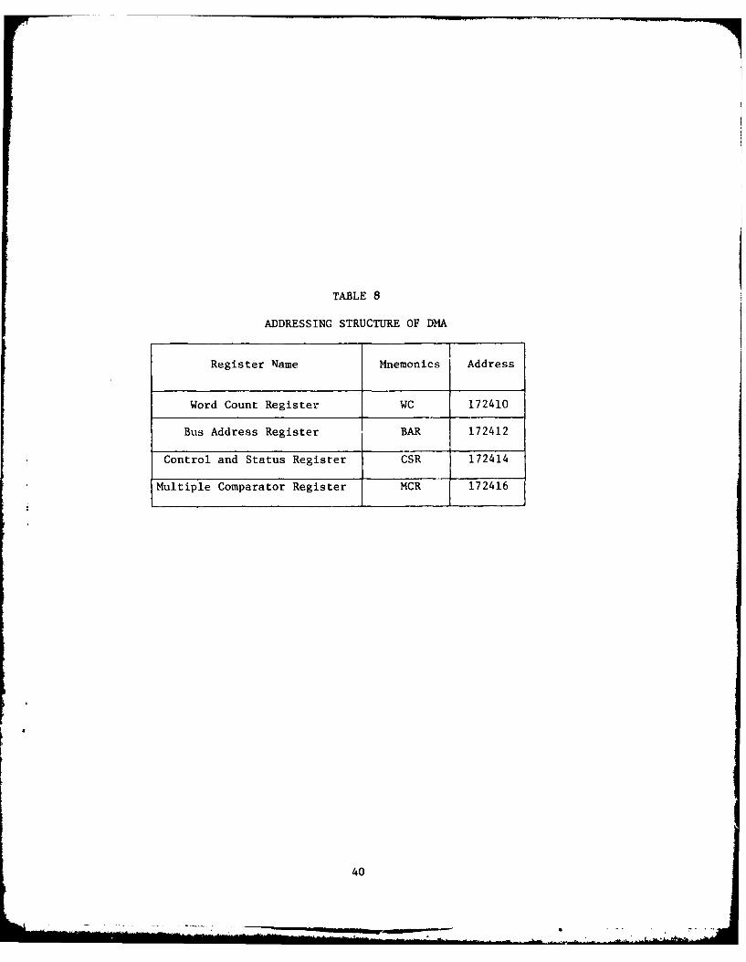
TABLE 8
ADDRESSING STRUCTURE OF DMA
Register Name Mnemonics Address
Word Count Register WC 172410
Bus Address Register BAR 172412
Control and Status Register CSR 172414
Multiple Comparator Register MCR 172416
40

BIT DESCRIPTION
Dl5 ERRORS (Read Only). Set by addressing nonexistent memoryor by grounding of external ATTN line. Cleared by systeminitialization, the clearing of D14, or clearing ATTN line.
D14 NEX (Read/Write). Nonexistent memory (NEX) is set byaddressing nonexistent memory.
D13 ATTN (Read Only). Indicates status of ATTN line.
D12-8 Not used.
D7 READY (Read Only): Indicates DMA is ready to start a newset of data transfers. Set by system initialization, wordcount overflow, and clearing of ERROR (D15).
D6 INTERRUPT ENABLE (Read/Write). Enables interrupts whenREAD~Y (D7) is set. Cleared by system initialization.
D5, D6 Extended Address Bits-17,16 (Read/Write).
D1-3 Not used
DO GO (Write). Starts DMA operation. Forces READY (D7) togo low.
Complete schematics for the ADAC 1620 DMA are given in Appendix C.
Further documentation for the DMA can be found in the IIDAC Instruction
Manuals, pp. 42-50 [9].
3.4 LSI-11 Software Description for the WQM
3.4.1 Fortran program
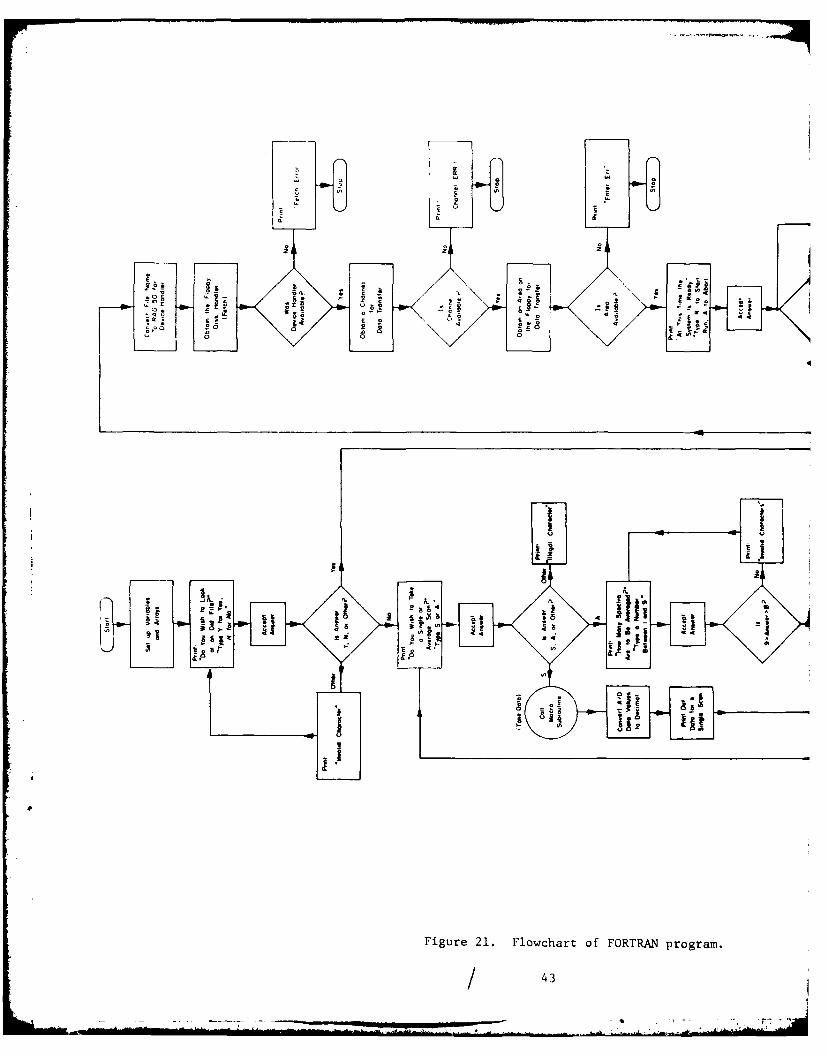
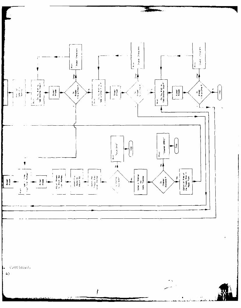
The Fortran program, AQSPEC (see Appendix E), is an operator interface
that leads the Weld Quality Monitor operator through a sequence of questions
to qualify and quantify the nature of the data desired. It also allows the
operator the opportunity to examine acquired data. A flowchart of the pro-
gram and a flowchart of the program as the user sees it are given in
Figures 21 and 22, respectively. The user is queried whether a single or
average set of scans is to be taken. If a single scan is desired for
41
2
I--
t
Figure 21. Flowchart of FORTRAN program.
/ 43

- 00
2 h
s *
r0 -42 2 40 -a-
&
owhr fFRRNporm43

0 IS
z!z
Figure 21. Continued.
45
/ 6--0 ... .. ... .-
- " l .. * ....
.-.
1 ilL2
j £
6
I
I ~ /
\ z -~.71~
I. 44
47
i
1'1~ -, e ~
7 I
/ ~0
'xx
-
-. ,. ~
1 440
0
~ .~a ~
-~C- C
t -3

2 C 00
zz
-0 CE CC 3E: 0
0~
0 -i
/447
-c.--

-r
0 00 0
E0 0 Z u0
a~~~ (n04
x
00
Userflowhartof FRTRA proram47
Ur flochr ofORRNpgam
calibration, a call to DMAIT (the Macro-il subroutine for data collection,
see next section) is made. If actual data are to be taken, then an average
scan is selected. The user must select the number of spectral scans that
the user wishes to have averaged together. Then, the user specifies the
total number of these averages that the user wishes to store and thereby
sets the amount of time used for data acquisition. It takes,on the average,
0.26 second for the head on the floppy disk drive to search and settle on
the floppy disk and 0.15 second to acquire, add, and write a spectral scan.
Thus, it takes about 1 second to acquire 5 scans, add them, and store them
on the disk. For the sake of expediting data acquisition, the voltage levels
taken from the AID are added together and stored as a sum. Division by
the number of scans is done when the data are outputted onto a peripheral
device.
j Data storage on floppy disks is accomplished through a set of Fortran
subroutines available with the RT-11 Fortran Library. These routines are
described extensively in the 1-li1 Operator Manuals, vol. 3, "Advanced
Programmer's Guide" [8]. Each file that is created on a floppy disk under
the RT-11 system is catalogued with a user-defined file name and its
subsequent creation date. The file, as it is created in AQSPEC, is sub-
divided into sets of 1024 words. The first 11 words are used to store the
date the data were taken, approximate time the data were taken, number of
scans averaged, arc voltage, arc current, and travel speed. Thus, the
first 11 photodiode voltage levels are overwritten. However, the next
1013 are intact.
Values stored directly from the A/D are not equal to the actual
voltages at the A/D input channel ports. The voltage conversion
specified by ADAC is given as follows.
49

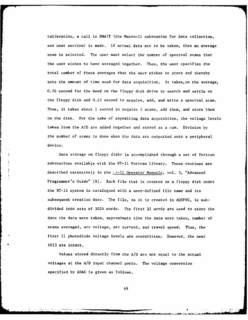
If the range is unipolar, look up the proper conversion factor from
Table 9 [9] and utilize the formula (1) shown below.
Voltage(decimal) = Conversion Factor(decimal) x A/D Output(decimal) (1)
If the range is bipolar, there are two separate procedures for negative
and positive voltages. For negative voltages, or decimal A/D values less
than 4095 and greater than 2046, find the proper conversion factor from
Table 9 [91 and utilize formula (2) shown below.
Voltage(decimal) = -Conversion Factor(decimal) x [4095 A/D Output(decimal) + 1]
(2)
For positive bipolar voltages or decimal values less than 2046 and
greater than zero, find the proper conversion factor and utilize formula (3).
Voltage(decimal) = Conversion Factor(decimal) x [A/D Output(decimal) + 11
(3)
Individual arc spectra with the accompanying time, date, arc voltage,
current, and travel speed can be displayed on the LA120 if desired. The
operator is also given the option of looking at other old files, or scans,
taking more data, or terminating the program. When the program has been
terminated, the terminal will respond with a ".". At this time, the power
bus can be shut off to power down all of the equipment.
3.4.2 Macro program
All data acquisition, DMA and A/D initialization and activation are
done in Macro-il, the DEC machine language. A copy of this program is
contained in Appendix D. A flov chart is given in Figure 23. An understanding
50
Ig
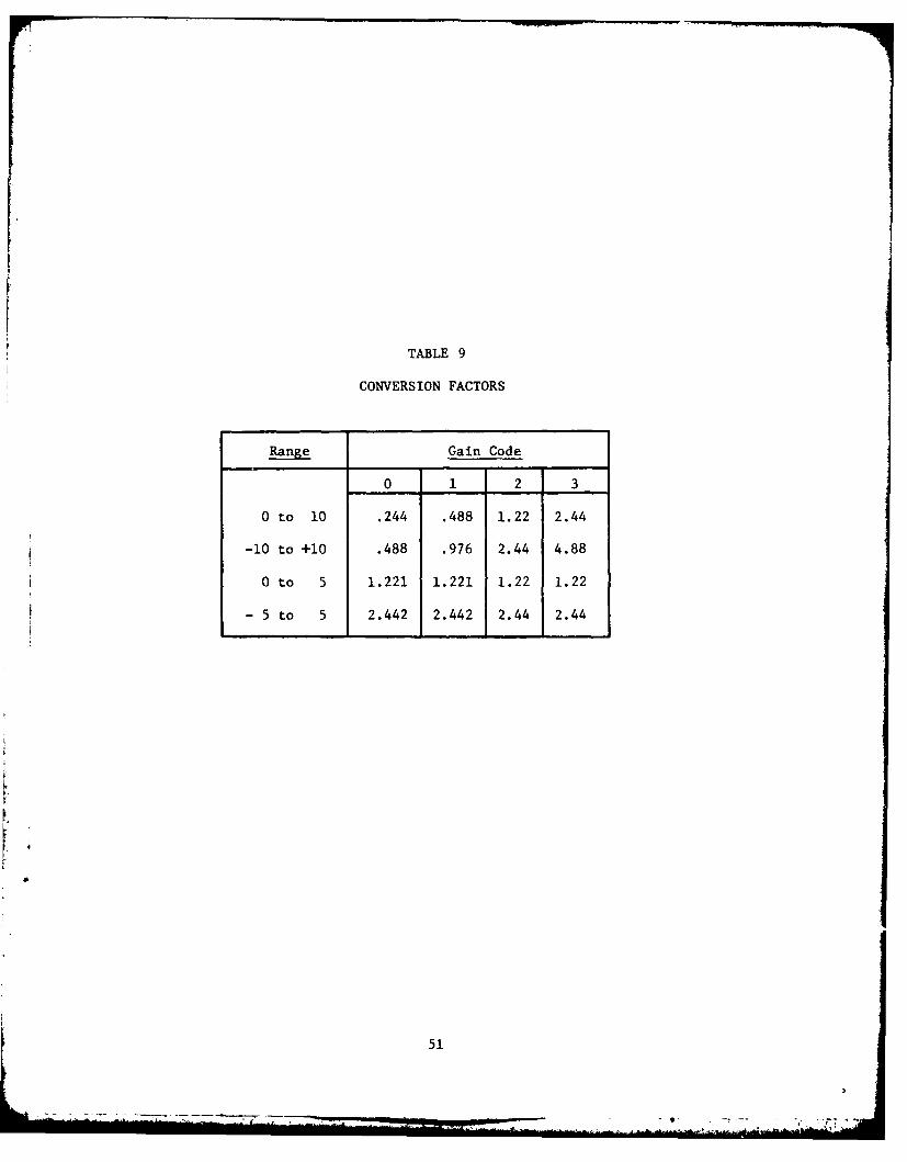
TABLE 9
CONVERSION FACTORS
Range Gain Code
0 1 2 3
O to 10 .244 .488 1.22 2.44
-10 to +10 .488 .976 2.44 4.88
0 to 5 1.221 1.221 1.22 1.22
-5 to 5 2.442 2.442 2.44 2.44
51

.00
0 v0E2
0 r
20 0-
(n Ou~ v
C) (n

zi
CC
10 C C
0
0C C)
Flwhr of mar program53L/n a4C
0~~

of the operation of the ADAC A/D and DMA, the synchronization circuitry,
and the Macro-li is needed to truly understand this program. This infor-
mation can be found in the appropriate section of this report with the
exception of information on Macro-li programming. Two reference sources for
this information are the DEC RT-11 Operator Manual [8], vol. 3, "Macro-ll
Language Reference" and Minicomputer Systems Organization, Programming,
and Applications (PDP-II), by Richard H. Eckhouse, Jr., and L. Robert Morris.
Two features of the program that are not described in the usual Macro-ll
documentation are .GLOBL, .TITLE, and .PSECT: RT-11 system macros. .GLOBL
is a system macro subroutine that allows the argument of the statement to
be accessed globally by other programs of the same or different languages.
.TITLE is a means of specifying a title for the program as listed in the
floppy directory. The .PSECT directive allows absolute control over the
memory allocation of a program at link time, because any program attributes
established through this directive are passed to the linker. The directive
is formatted as follows: .PSECT name, argl, and 2, ..., argn. Name
represents the symbolic name of the program section. Arg represents one
or more of the legal symbolic arguments defined for use with the .PSECT
directive. The arguments are described in the following manner:
ARGUMENT DEFAULT DESCRIPTION
RO/RW RW RO = Read-Only AccessRW = Read/Write Access defines which
type of access is permitted to theprogram section.
I/D I Defines the program section as
containing either instructions (I)or data (D).
55

ARGUMENT DEFAULT DESCRIPTION
GBL/LCL LCL Defines the scope of the program section,as iubsequently interpreted at link time.If an object module contains a local pro-gram section, then the storage allocation
for that module will occur within thesegment in which the module resides. Many
modules can reference this same programsection. If an object module contains aglobal program section, the contributions
.to this program section are collectedacross segment boundaries, and the allo-cation of memory for that section will gointo the segment nearest the root in whichthe first contribution to this programsection appeared.
ABS/REL REL Defines the relocatability attribute of
the program section. ABS = Absolute(nonrelocatable). When the ABS argument
is specified, the program section isregarded at link time as an absolutemodule, thus requiring no relocation.REL = Relocatable. When the REL argu-
ment is specified, the linker calculatesa relocation bias and adds it to allreferences to locations within the pro-
gram section.
CON/OVR CON Defines the allocation requirements of
the program section. CON = Concatenated.All program section contributions are tobe concatenated with other references tothis same program section in order todetermine the total memory allocation
requirement for this program section.OVR = Overlaid. All program sectioncontributions are to be overlaid. Thus,the total allocation requirement for theprogram section is equal to the largestallocation request made by any individualcontribution to this program section.
For further information on this directive, see the RT-11 Operator
Manuals, "RT-lI Advanced Programmer's Guide," Section 6.8.1, pp. 6-32;
6-36 [8].
The following is a step-by-step description of the Macro program
itself.
56

1) .TITLE INIT.MAC
The .TITLE macro directive is used to place the title of the program
at the top of the program li :g. In this case, it is INIT.MAC.
2) .GLOBL DMAIT
The .GLOBL macro directive is used to allow the argument of the
directive to name a program section that can be collected across
segment boundaries in memory. In this case, DMAIT is made available
to the FORTRAN program AQSPEC.
3) DMAIT: TSTB @#172414
DMAIT: is a label used to name this line of code for external reference.
TSTB translates to TeST Byte. This command sets the condition codes
for the processor status word in the microcomputer. Since the test
is performed on the lower byte of the word 172414, the seventh bit
will determine the sign of the byte. The seventh bit is the sign
bit of a byte in two's complement arithmetic. Bit 7 of word 172414
is the busy bit on the DMA Control Status Register. If it is equal
tzi a 1, it is negative; if it is 0, it is positive.
4) BPL DMAIT
BPL translates to Branch if PLus. If the BUSY bit is a one (bit
seven is a sign bit on a two's complement byte) or negative, go to the
argument of this command: DMAIT. If it is not a 1, continue to the
next instruction in the program.
5) MOV #176000, @#172410
The MOV command takes the first operand, 176000, and moves it into
the second operand, @#172410. The actual number 176000 (i.e., -1024
decimal) is moved into the word at location 172410 in the memory.
57

172410 is the Word Count Register (WCR) in the DMA. The WCR stops
DMA transfers when its content equals zero. After each DMA transfer,
the WCR is incremented by one. Thus, 2000 octal transfers or 1024
decimal transfers will be made before the WCR equals zero.
6) MOVTOT,@#172412
The effect of this command is to place the memory address associated
with the label TOT (TOT is the first word location in a linear array
that is 1024 elements long) into the Memory Address Register (MAR)
in the DMA. The MAR is used to keep track of the current location
for the data storage. It is incremented after each data transfer.
7) MOV #1,@#172414
The effect of this command is to place a 1 in the least significant
bit of the word at location 172414. Location 172414 is the DMA
Control Status Register (CSR). The bit in question allows the DMA
to be enabled.
8) MOV #1,@#172416
Location 172416 is the Multiplex Comparison Register (MCR) in the
DMA. The MCR is used if conversions on eaih channel are to be done
sequentially from channel to channel. Since we wish to sample one,
a one is placed in the MCR to indicate that only one channel is to be
sampled.
9) MOV #32,@#177000
Location 177000 is the Control Status Register for the A/D. The octal
value of 32 configures the A/D for an external enable or trigger, unity
gain, and conversion on channel 0.
58

10) MOV #1,0#167772
This command will set the output channel 0 high (+5 V) on the parallel
I/0 board. This enables the synchronization circuitry to begin
triggering of the A/D.
11) 1$: TSTB @#172414
BPL 1$
Until 1024 conversions and data transfers have been completed the
BUSY bit in the DMA CSR will be set equal to a 1. When it is set
equal to a 0, the program will continue.
12) MOV #0,@#167772
This command sets the output channel 0 on the parallel I/O board
to ground so that the synchronization circuitry is disabled.
13) MOV #0,@#172414
This command will disable the DMA.
14) MOV #431,@#177000
The octal number 431 will force a conversion with unity gain on
channel 1 of the A/D. Channel 1 is the weld arc voltage.
15) LPI: TSTB @#177000
BPL LPl
When bit 7 of the A/D CSR is set, the A/D has not finished a
conversion. When the A/D finishes, the program will continue.
16) MOV #TOT+6.,Rl
The memory location TOT plus the decimal value of 16 will equal the
ninth word in the linear array following TOT. This word will be
used to store the value of the voltage. Rl is a general-purpose
register in the LSI-11/23 microprocessor that will be used to point
to locations in the array.
59

17) MOV @#177002,(RI)+
Location 177002 is the data buffer for the A/D. Since step 15 has
been completed, the data buffer will contain the converted value
for the voltage. (Rl)+ has the effect of opening the contents of
the location of the address pointed to by the value in R1 for
deposit of the converted value for voltage. The + increments the
value of Rl by 2 after the completion of the instruction, thus forcing
RI to point to the next word in the array TOT.
18) MOV #1031,@#177000LP2: TSTB @#177000
BPL LP2
MOV @#177002,(Rl)+
The instructions above perform the same function as steps 14, 15,
and 17; however, they apply to channel 2 on the A/D which has the
weld arc current as an input.
19) MOV #1431,@#177000BPL LP3MOV @#177002,(R1)
These instructions perform the same function as steps 14, 15, and 17;
however, they apply to channel 3 on the A/D which has the weld travel
speed as an input.
20) ENDI: RTS PC
RTS translates to ReTurn from Subroutine. PC is the Program Counter
and must be restored to its original value before the subroutine
was called so that the computer can start at the right location in
the calling program.
60

21) .PSECT TOT,RW,D,GBL,REL,OVR
A complete description of the macro directive PSECT is given just
prior to this section of text.
22) TOT: .BLKW 1024.
.BLKW translates into BLocK of Words. This macro directive has the
effect of creating an array of words which is as long as the number
following the dirertive. 1024. forces the number to be considered as
a decimal number as opposed to an octal one. Thus, the array is
1024 words long. TOT is a label that will be set equal to the
value of the memory location of the first word in the array.
23) .END DMAIT
This macro is used to define the absolute end of the program. Its
argument must reference the first executable statement of the program.
It should be noted that Macro-ll code, as In this case, is usually only
used when speed and efficiency are required.
61
;. -P I

4. OPERATING PROCEDURE
Before data acquisition can be accomplished, the following cables
must be connected. The numbers circled refer to the corresponding numbers
in the figures on pages 68-75 unless otherwise specified.
1) Be sure all power lines from devices on the rack are plugged into
the power bus at the top of the rack. At this time, do not plug the
power bus into an outlet.
2) All boards should be firmly secured in the back plane of the
LSI-11 housing.
3) Six cables that must be in place at this time are: a ribbon
cable from the RX02 floppy disk drive to the RXV21 board Q(Figure 24); a ribbon jumper cable from the A/D to the DMA
(Figure 25); a shielded ribbon cable from the A/D to the
spectrograph control box ( (Figures 24, 25, and 26); a cable
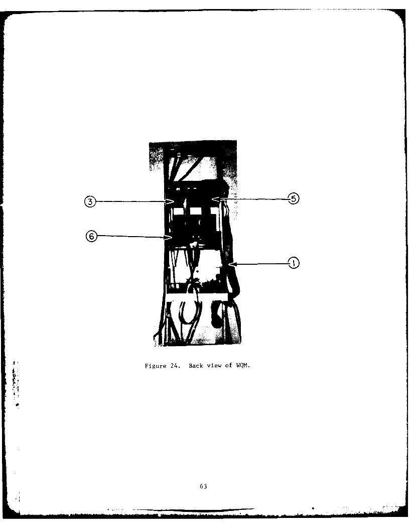
running from channel 3 of the DLV-J serial interface board to the
Decwriter LA-120 @ (Figures 25 and 27); a ribbon cable running
from the MDB MISI-DRVlI-C parallel interface board to the spectro-
graph control box 0 (Figures 24, 25, and 26); and a ribbon cable
running from the spectrograph control box to the spectrograph @
(Figures 24 and 26). With the exception of the last cable mentioned,
none of these cables should be removed while the computer is powered
up.
62
-0
Figure 24. Back view of WQM.
63

Fi1,uru 25. Backplane of DEC minicomputer.
v9
PA00
Figure 26. Back of spectrograph control box.
64
14
Figure 27. Decwriter LA-120.
65

t V iI, o i spectrum i, des red , conri ct onl. -nd
1 n tENt -'ab lc to t h SIART OUT Q (Figure 28) on the spectrograp
Control box and th, othIwr to tht. 1,u 'i1loscope trigger. Connect another
ENC to thu VIDEO OUT (Figurc 21") on the spectrograph control box
and an inverted e hr;in ]I en the same scope.
5) If voltage, current, and travel speed are desired, connect the
a :propriate BNC's to the back of the spectrograph control box
1Figure 26). The range of these inputs must be restricted to 0-10 V.
If these ports are not to be used, they must be shorted for the vroper
operation of the system.
6) Plug the power cord from the power bus into a 110 V outlet and
turn the bus on. The sstem is now ready for initialization.
After the steps abov, have been completed, the following procedure
can be used to initialize the aoftware for data acquisition.
1) Turn the computer power switch @ (Figure 29) and the
spectrograph control box power switch © (Figure 28) on.
2) Take the RT-11 system software and data acquisition floppy
disk and slide it into slot 0 102 (Figure 30) in the RX02 disk
drive. Close the door over the slot. (The slot cover is opened
by depressing a button under the handle on the slot cover.)
3) Slide a formatted and initialized data floppy disk (see Appendix B)
into slot 1 @ (Figure 30) in the RX02 disk drive and close the door.
66

0
Fi ,,url< 28. Front of spectrograph control box.
k 1now.--

Figure 30. Front of WQM.
6 8

4) Turn the LA120 power switch (Figure 27) on.
5) Check to see that the LA120 indicator light is "ON LINE"
rather than "LOCAL" @ (Figure 31) [10]. If it is on "LOCAL,"
press the ON LINE/LOCAL button @ (Figure 31) [10].
6) Press the system initialization button @ (Figure 29) and
wait for this response on the LA120:
UI PHYSICS RT-11FB (S)VO3B-02
?KMON-F-File not found
The following information will detail the computer interface with
the WQM operator and the possible responses. A 0 , will precede anything
that the computer will type at the terminal. The response by the user is
underlined. After the possible user response, there will be a description
of the computer action taken and the step number of the next question.
7)0 ;This is the computer prompt.
DATE 7-JUL-81 ;The date shown is represen-tative of the way the dateis entered.
8)0
TIME 13:48:00 ;The value for the time isarbitrary but illustratesthe way time is enteredinto the system.
Note: The date and time must be reset
*for every system initialization. Also,
to erase characters entered, type the
delete button until the error is reached.
Then, retype the information to correct
the mistake.
69
______ Now--_ S.-

15 16
AA."T TUo A
TS CEAR TA" top 00PT "CAS STAS CU M O WNE
SIT CPLEA . To T A 'f STATSALSAW U N
Figure 31. Keyboard f or DecWriter LA-120 [10].
Copyright@©1979, Digital Equipment Corporation.
All Rights Reserved. Reprinted with permission.
70
OWN' -unueu;ununa
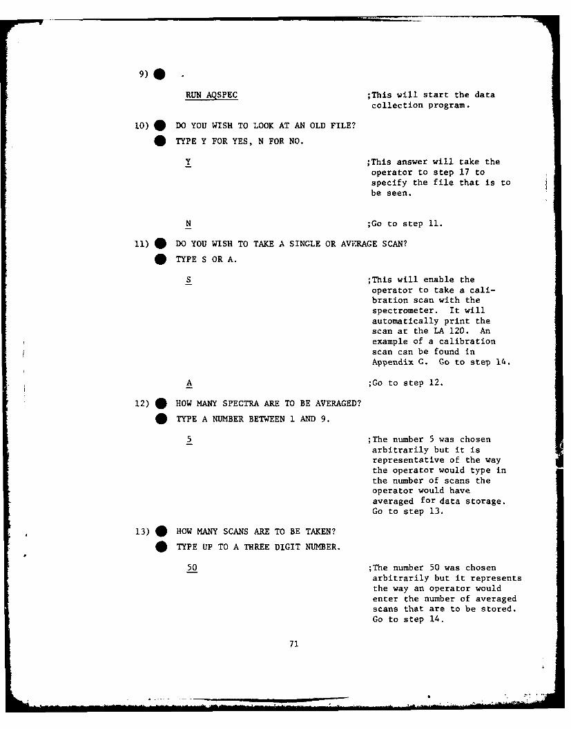
RUN AQSPEC ;This will start the data
collection program.
10)10 DO YOU WISH TO LOOK AT AN OLD FILE?
*TYPE Y FOR YES, N FOR NO.
Y ;This answer will take theoperator to step 17 tospecify the file that is tobe seen.
N ;Go to step 11.
11) *DO YOU WISH TO TAKE A SINGLE OR AVF.RAGE SCAN?
*TYPE S OR A.
S ;This will enable theoperator to take a cali-bration scan with thespectrometer. It willautomatically print thescan at the LA 120. Anexample of a calibrationscan can be found inAppendix G. Go to step 14.
A ;Go to step 12.
12) * HOW MANY SPECTRA ARE TO BE AVERAGED?
*TYPE A NUMBER BETWEEN 1 AND 9.
5 ;The number 5 was chosenarbitrarily but it isrepresentative of the waythe operator would type inthe number of scans theoperator would haveaveraged for data storage.Go to step 13.
13) * HOW MANY SCANS ARE TO BE TAKEN?
* TYPE UP TO A THREE DIGIT NUMBER.
50 ;The number 50 was chosenarbitrarily but it representsthe way an operator wouldenter the number of averagedscans that are to be stored.Go to step 14.
71

14) *ENTER A SIX CHARACTER CODE WORD HERE.
TESTOO ;This word can be anycombination of six or feweralphanumeric characters.It will be used on thefloppy disk directory toname the file created. Allreferences to this datafile must be done with thefile name in the future.Go to step 15.
15) *AT THIS TIME THE SYSTEM IS READY.
*TYPE R TO START A RUN OR A TO ABORT.
A ;This command will terminatethe acquisition of data aspreviously specified. Nofile will be created and nodata will be taken. Go tostep 12.
R ;This command will begin thedata acquisition andstorage. When the computernext responds with aquestion, the data will havebeen taken and stored under
the code word specified
earlier. Go to step 16.
16) *DO YOU WISH TO SEE THE RESULTS?
N ;Go to step 11.
Y ;This command will allow theoperator to view the dataon the LA 120. Go to step17.
17) *WHAT FILE CODE DO YOU WISH TO ACCESS?
*TYPE A SIX CHARACTER CODE WORD.
TESTOO ;The code word shown is justfor purposes of illustration.It can be any six or feweralphanumeric characterscorresponding to an existingfile on the floppy disk inslot 1 of the floppy diskdrive. Go to step 18.
72

18) * TYPE A THREE DIGIT SCAN NUMBER.
28 ;The number shown was
arbitrarily selected. Itcan be any number thatcorresponds to a set ofaveraged spectral scansstored in the file speci-fied in step 8. The numbermust correspond to a numberless than or equal to thetotal number of average scanstaken for that file. Thescan specified will beprinted out automatically.An example of the output isshown in Appendix F. Go tostep 19.
19) * DO YOU WISH TO SEE ANOTHER SCAN?
* TYPE Y FOR YES, N FOR NO.
Y ;This question asks the
operator if he would liketo see another scan numberin the same file that wasopened in step 8. With
this command, the operatorwill proceed to step 18.
N ;Go to step 20.
20) * DO YOU WISH TO SEE ANOTHER FILE?
TYPE Y FOR YES, N FOR NO.
Y ;This question will allowthe user to access any filethat exists on the floppydisk in slot 1 of the
floppy disk drive. Withthis answer the operatorwill proceed to step 17.
N ;Go to step 21.
21) 0 DO YOU WISH TO TAKE ANOTHER SCAN?
TYPE Y FOR YES, N FOR NO.
Y ;This question asks theoperator if he wishes to
continue taking data. Withthis answer the operatorproceeds to step 11.
73

N ;This answer will terminatethe program. Wait for thecomputer to respond with
its prompt before rerunningthe program or starting thepower off procedure.
22) To stop operation, turn off the power switch on the LA 120
and the power bus at the top of the rack.
t
74-M if .

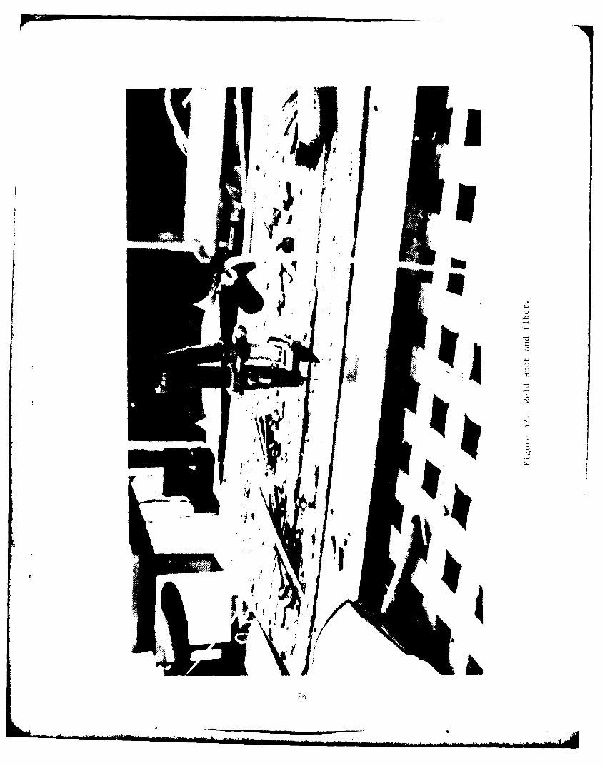
5. EXPERIMENTAL RESULTS
To illustrate the capabilities of the system, results of two experiments
are described in this section. Both experiments were bead on plate tests
using the shielded metal arc welding process with argon shielding gas, carbon
steel base metal, and E70S-3 electrodes (see Figure 32).
In the first experiment, the argon shielding gas was interrupted during
the welding process and the resultant changes in the arc spectrum, voltage,
and current observed. Complete or partial loss of shielding gas can cause
flaws such as porosity and slag in the weld joint. In the past, attempts
have been made by other workers to monitor shielding gas flow using pressure
transducers; this approach has not been very successful. The experimental
procedure was as follows:
With thL shielding gas on, the arc was stabilized bv adjusting th(t current
to 300 A. Data collection was then initiated by the computer and continued
for 50 seconds. Samples of the arc spectrum, voltage, and current were
averaged for one-half second and then stored on a disk. Because the access
time for the disk is approximately one-half second, data were collected at
one-second intervals. Approximately 10 seconds after data collection was
initiated, the argon shielding gas was turned off for 10 seconds. Shielding
gas was turned on at 20 seconds, off again at approximately 30 seconds, then
on at 40 seconds.
Figure 33 is a plot of the arc voltage and current versus time. The
times during which the shielding gas was off are clearly evident. When the
shielding gas is turned off, the arc current decreases from 300 A to approxi-
mately 250 A, and the arc voltage incrcases from 30 V to approximately
75
~j~Iw I'I
t N
I-4-c
'~1
44

S I I " I i I -
40
VOLTAGE
-400
l",./- , " ' --300 l
- CURRENT -
10- 200
0 10 20 30 40 50
TIME (s)
Figure 33. Variation of the arc voltage and current versus time.The argon shielding gas was interrupted twice duringthis experiment for approximately ten seconds each time.The shielding gas was turned off at approximately9 seconds and again at approximately 29 seconds.
77
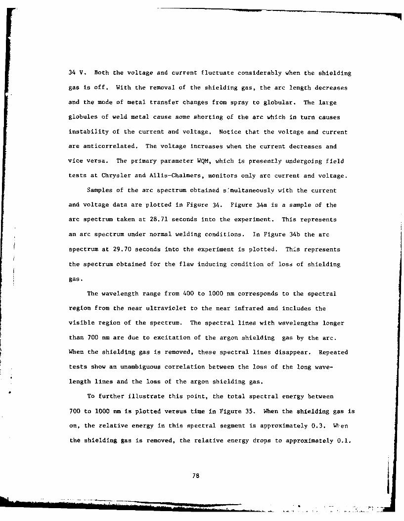
34 V. Both the voltage and current fluctuate considerably when the shielding
gas is off. With the removal of the shielding gas, the arc length decreases
and the mode of metal transfer changes from spray to globular. The large
globules of weld metal cause some shorting of the arc which in turn causes
instability of the current and voltage. Notice that the voltage and current
are anticorrelated. The voltage increases when the current decreases and
vice versa. The primary parameter WQM, which is presently undergoing field
tests at Chrysler and Allis-Chalmers, monitors only arc current and voltage.
Samples of the arc spectrum obtained smultaneously with the current
and voltage data are plotted in Figure 34. Figure 34a is a sample of the
arc spectrum taken at 28.71 seconds into the experiment. This represents
an arc spectrum under normal welding conditions. In Figure 34b the arc
spectrum at 29.70 seconds into the experiment is plotted. Th.is represents
the spectrum obtained for the flaw inducing condition of loss of shielding
gas.
The wavelength range from 400 to 1000 nm corresponds to the spectral
region from the near ultraviolet to the near infrared and includes the
visible region of the spectrum. The spectral lines with wavelengths longer
than 700 nm are due to excitation of the argon shielding gas by the arc.
When the shielding gas is removed, these spectral lines disappear. Repeated
tests show an unambiguous correlation between the loss of the long wave-
length lines and the loss of the argon shielding gas.
To further illustrate this point, the total spectral energy between
700 to 1000 nm is plotted versus time in Figure 35. When the shielding gas is
on, the relative energy in this spectral segment is approximately 0.3. WV1en
the shielding gas is removed, the relative energy drops to approximately 0.1.
78

3.0 1 1 i I '
TIME2.5- 28.71 sec.
0 2.0-
1.5
> -
0.5i
0.0400 500 600 700 800 900 1000
(a) WAVELENGTH (nm)
3.0 1 I 1 1
TIME2.5- 29.70 sec.
> 2.0-
C, 1.5-
o 1.0-
0.5
0.0400 500 600 700 800 900 1000
(b) WAVELENGTH (nm)
Figure 34. Typical examples of the arc emission spectra. Figure 34ais a spectrum obtained at 28.71 seconds into the experi-ment and corresponds to normal welding conditions wherethe argon shielding gas is on. Figure 34b is a spectrumobtained at 29.7 seconds into the experiment and corre-sponds to abnormal welding conditions when the shieldinggas is off.
79
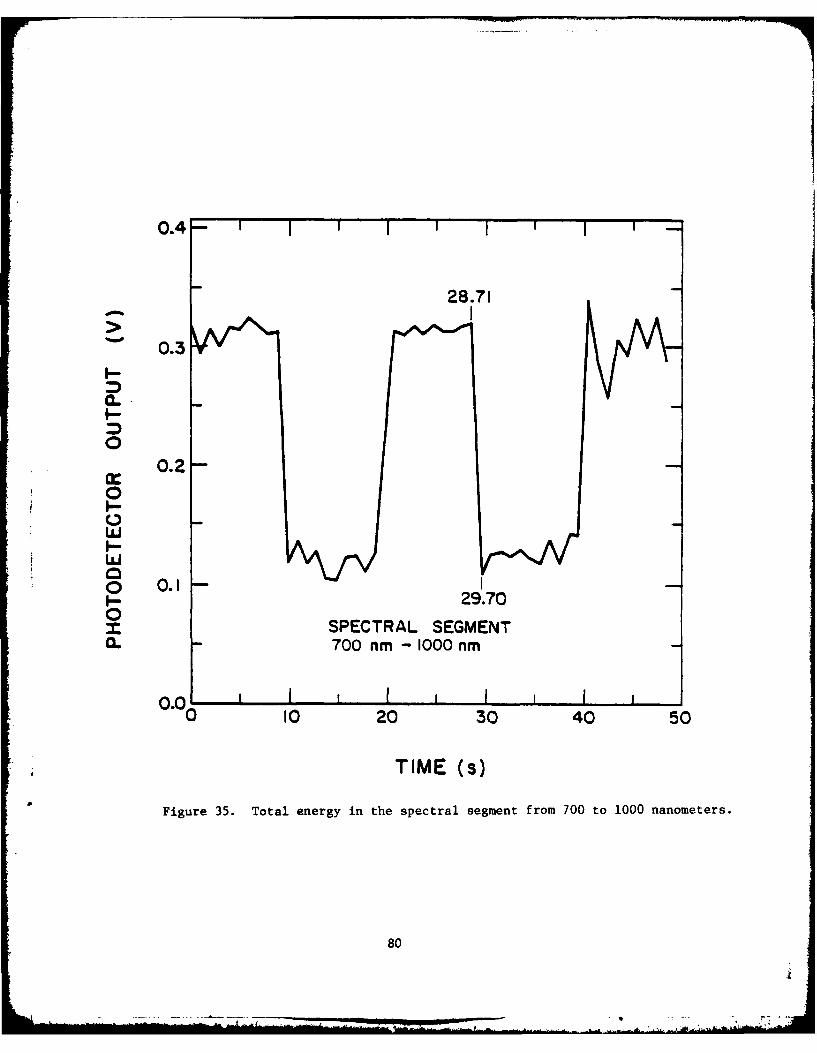
0.4- 1 1
28.710.3I-.0~0.-0ww0 0.1 o u.'29.700
x SPECTRAL SEGMENTCL 700 nm - 1000 nm
00 10 20 30 40 50
TIME (s)
Figure 35. Total energy in the spectral segment from 700 to 1000 nanometers.
80

The times annotated on Figure 35 correspond to the times at which the spectra
in Figure 34 were obtained (28.71 seconds and 29.70 seconds). The data
plotted in Figure 35 show that a complete loss of the shielding gas occurs in
less than one second. Although the time resolution of our system was one
second for this experiment, it can be increased to less than one-tenth of
a second, if necessary. Notice that all of the spectral energy was not
lost when the shielding gas was off. The residual energy in the 700 co
1000 nm wavelength range is due to black body radiation from the weld arc.
It may be possible to determine thle temperature of the arc by fitting the
background spectral energy to the standard black body curve.
The total energy in the wavelength region between 400 and 700 run is
plotted in Figure 36. Although the energy does decrease in this region when
thle shielding gas is removed, the decrease is not as abrupt nor as significant
as that plotted in Figure 35. We believe the gradual decrease in energy is due
to the increase in smoke production when the shielding gas is interrupted.
The shorter wavelengths are attenuated by the smoke much more than the longer
wavelengths. Consequently, it is smoke that is attenuating the shorter wave-
lengths rather than loss of argon emissions in this spectral region. When
the shielding gas is turned on, the energy does not abruptly increase. It
takes awhile for the smoke to be cleared from the welding area. Notice
also that when the shielding gas is off, the energy fluctuates considerably
more than the energy in the 700 to 1000 rim region. The total energy
from 400 to 1000 nm versus time is plotted in Figure 37. This plot shows
the combined effect of loss of shielding gas on the near UiV, visible,
and near IR regions of the arc spectrum.
81

0.7-
> 0.6-
a. 0.5
0.-
0
0.3-
wo 0.2-0
x SPECTRAL SEGMENTCL 0.1400 nm - 700 nm
0.0 I0 10 20 30 40 50
TIME (s)Figure 36. Total energy in the spectral segment from 400-700 nanometers.
82f

0.6
On% 0.5 -
0.4a-
0
x 0.3-0
w0.2-
0
00.1I SPECTRAL SEGMENT
400 nm - 1000 rim
0.0 I0 10 20 30 40 5b
TIME (s)Figure 37. Total energy in the spectral segment from 400 to 1000 nanometers.
83

Figure 38 is a plot of the energy in the argon line from "14 to 816 nm.
The energy in this line changes by almost a factor of six when the shielding
gas is removed. Obviously, a very simple shielding gas monitor could be
constructed by using a narrow-band filter and photodetector to measure the
spectral energy in the 814 to 816 nm wavelength region.
The physical results of loss of shielding gas are easily seen in macro
etched cross sections of the welds made in this experiment. Figure 3 9a is
the normal weld (shielded), with deep weld metal penetration, a fairly small
heat affected zone, and an absence of visible slag inclusions or porosity
defects. In Figure 39b the weld made without shielding gas is shown. The
weld contains gross porosity, a slag inclusion,and a large heat affected zone.
The shape of the weld bead is also flatter and more irregular than that of
the sound weld.
The second experiment was designed to determine the correlation between
heat input and the arc spectrum. Heat input is defined as the arc current
times the arc voltage divided by the travel speed, and is usually given in
units of kilojoules per inch. In this experiment the heat input was varied
by varying the arc current. Figure 40 is a plot of the current and voltage
as a function of time. The current was vaiied from approximately 200 to
360 amperes. Since the travel speed was constant at ten inches per minute,
this corresponds to a variation in the heat input from approximately 36 tQ
55 kilojoules per inch.
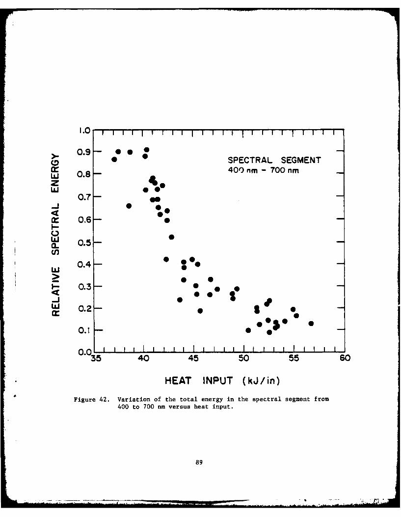
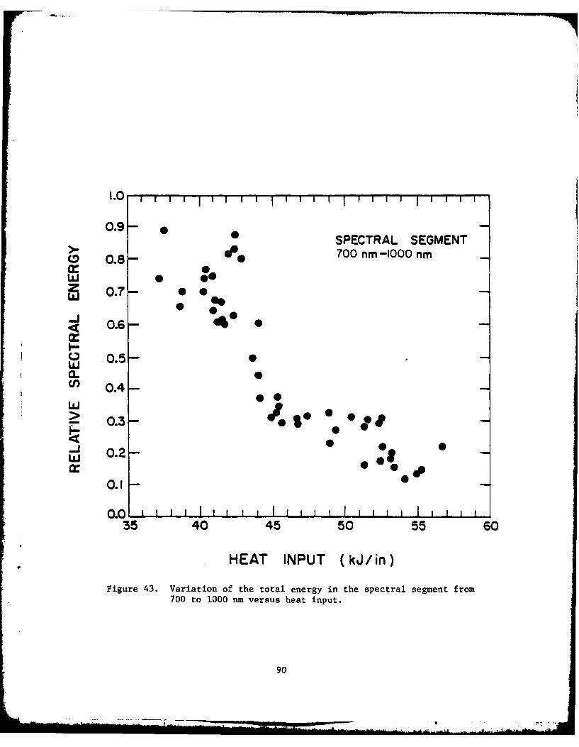
Figure 42 is a plot of the total spectral energy from 400 to 1000 nm as
a function of heat input. Figures 42 and 43 are similar plots for the energy
in the 400 to 700 nm region and 700 to 1000 nm region, respectively. In all
84
. . ... .. . . . . . f.. .. . ... .. . " . ....._ _. ....._ _. . .._ _-
__ _ _-__ _ _' S° ' " ' "

0.7 II
0.6
0.5-0L
o 0.4-
0a: 0.0wLii o 0.2-
0x 0.1
CL SPECTRAL SEGMENT814 nm - 816 nm
0.0 1 1 1 1 1L I I0 10 20 30 40 50
TIME (s)Figure 38. Total energy in the spectral segment from 811 to 816 nanometers.
85
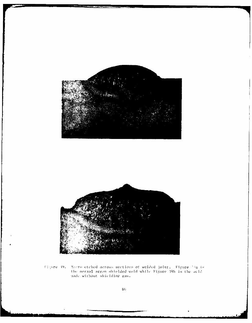
H 31) 1 ir() etched across sect iom; of weled ,joint. Figure l a isth1w normal a rgon shielded weldi wh i Ic Fi gure !39b is the .seI(I!7ii c witholit shi1ttlinp gas.
86

400
35- CURRENT
IV'
> - 300
w D->z
20025 VOLTAGE
20 I 1. 1 I1i 00
0 10 20 30 35 40
TIME (s)Figure 40. Variation of the arc voltage and current versus time. The arc
current was varied between approximately 200 and 360 A.
87

1.0 I I i I I I' I I I i I I I i
0.9-
S0.8-SPECTRAL SEGMENTw
z 0.7 400 nm -1000 nm.7
< 0.6-
I-- O .5-wa3.cn 0.4-
> 0.3-
0.2- %0.1- 0 %• 0
0.0 , , I 1 1 1 I I I I 'I' '35 40 45 50 55 60
HEAT INPUT (k/in)
Figure 41. Variation of the total energy in the spectral segmenL from400 to 1000 nm versus heat input.
88
1.0 I I f
0.9 SPECTRAL SEGMENT40'0 rm - 700 nmw 0.8-
z 0w0.? g
c0 0.6
0.6-I-
0.4- 0
0.5-
w 00 0
I- 0.3 0
35 40 45 50 55 60o
*HEAT INPUT (WJ/in)
Figure 42. Variation of the total energy in the spectral segment from400 to 700 ran versus heat input.
89
SPECTRAL SEGMENT
(D 0.8- 700 nm-I000 nm
z 0.7
0.6 4I--0. 0.5 0
Cn 0.4-w @
0.230
0.1
35 40 45 50 55 60
HEAT INPUT (kJ/in)
Figure 43. Variation of the total energy in the spectral segment from700 to 1000 tim versus heat input.
90

three cases the general trend is for the spectral energy to decrease as the
heat input increases. However, the decrease seems to be more pronounced
and more systematic for the wavelength region between 400 to 700 nanometers.
Because different regions of the spectrum behave differently as the heat
input is changed, it may be possible to compute the heat input directly from
the spectral data.
Both of the experiments described have been repeated several times at
the CERL Welding Laboratory over a six-month period. Excluding hardware
anomalies, the same results were obtained.
The real-time weld arc spectrum detection and analysis capabilities of
this prototype optoelectronic system are demonstrated by the data presented.
The confidence level of the system was established by reproducibility of
results during the six-month testing period. An area for future development
is resolution. Resolution improvements may prove to give additional weld
quality information. In particular, hydrogen and sulfur contaminants may
be detectable. Another area of development is tha development of heat
input/arc spectra correlation. This may be accomplished with a broader
data base.
91
- --
6. CONCLUSIONS
This report has described the software and hardware designs of the
electro-optic Weld Quality Monitor. The system was developed to study
the spectral and electrical characteristics of the weld arc. Included
was a representative sample of data that was collected with the system.
It is clear from observing changes in the weld arc spectrum that changes
in arc voltage, current,and shielding gas flow are easily discernible
in argon gas shiel.ded welds. Additional experiments using different
welding techniques are needed to establish the applicability of this
system. Currently, weld parameter standards are either nonexistent or
crude at best. It is hoped that, with the continued use and refinement
of this system, standards will be established that provide improved weld
integrity.
92
- ,it~-

APPENDIX A
SPECIFICATIONS AND SCHEMATICS ON RETICON DIODEARRAY AND SCANNING ELECTRONICS
93

ALIGNMENT PROCEDURE FOR THE RC-lOOB MOTHERBOARD WITHRC-104, 105, OR 106 AND "G" SERIES ARRAY
1) Jumper Connections. Split pads are provided to program the RC-IOOB
board for the desired configuration. Refer to p__ (Drawing
Number 011-0238)for correct configuration.
2) Monitor . Adjust R2 for the desired frequency, 1 MHz maximum.
Adjust R11 for a 700 ns negative going pulse width.
3) Monitor P2-b. Set the desired start pulse interval, using rocker
switches Sl, S2, and S3.
4) Monitor TP2 and adjust R64 for a 100 ns pulse width.
5) Darken the array, monitor Jl-l, and adjust R4 (put on the component
side of the array board) so that the video signal is approximately
centered at -5 V DC. Saturate the array, and readjust R4, if necessary,
so no signal or switching spike is more negative than -8 V DC.
Do not over-saturate.
6) Monitor P2-N. The video output will be a sample-and-hold boxcar
signal.
7) Darken the array and adjust R36 until the video signal is centered
around the blanking level. (Blanking is clamped at zero.)
8) Adjust Rll until optimum performance is observed on the video.
Optimum adjustment of R11 results in a balance of maximum video
output, minimum switching spikes, and fixed pattern tracking from
dark to 90% of saturation.
9) With the array in the dark, readjust R36 if necessary to bring the
video level with blanking.
94

SPECIFICATIONSELECTRICAL CHARACTERISTICS (25-C) ELECTRO-OPTICAL CHARACTERISTICS
Min Typ Men Units'Positive Supply Min Typ Max Units
voltage V. 0"5 *5 .5 volts Diode Center-to-Negative Supply Center Spacing - 25 - Aim
Voltage V, -10.5 -10 -9.5 volts Diode Aperture Width - 26 - innClock Voltage Low Vc, -10.5 0 -1 volts 3fPhottOiodi Senstvty - 2.5 - p"ll tticfft'Clock Voltage High VcI, V -1 +5 Vp volts 3NoEI-uniformity ofStart Voltage Low V,1 -10.5 0 +1 volts Serisitivity,Start Voltage High Viii Vp -I +5 Vp volts AL-12BG - 4 8 *%Clock Pulse Width 0,2 - - uscRL-256G - 4 a 1%
Start Pulse Width See Fig. 7 L52- S o %
Clock Frequency fc - - 1 MzRL-12G - S 14 t%
Integration Time ti - - 30 msec2Clock Input
Capacitance Cc - 5 - pF iSaturation Exposure - 1.3 - ujoulescm'
'Start Input Saturation Charge - 3.2 - pcoulCapacitance C, - 5 - P
'Video LineCapacitance C,, NOTSC
RL-1024G - 40 - pP 1 No terminal should eve be allowed to go wrore positive than VP.RL-512G - 20 - pP 2 Measured with nomninal power supply votegs.
AL-256G - 10 - ~p I Measured Using light so0urcell of Fig 4.
RL-128G - 5 - pFEnd-of-Scan OutputResistance - 5 - Kohm0-C Power Dissipation - 45 - mwatts
(From~ Reticon~ Corp.)
95

. .. .......... -c
..... .+.. . _ . . , , i . + ,
- --- 4I1, _ I
iII
• , I
- . ' '
. . . |4 '
, . . 4.:_ 4, t ; - . . v, , I,, Ci ,4'4, '+ :. -4 -4. - , ,,
.0 i
**7
: + + . . ' - -W ' - r , +,
"' ,". 4
. .o,5 . , , ,. - .- - > . ,.. . . ..
: .+ + ' ' ' ',- - .. .
*,L+ 1-+ --,0 , .----.-- '4,,-, . 4 1,.4 ',._-'" _-- ---- _' __ ,_____-__-_____-______, "__--" " ___ .. . . .
-0. .t , ' .- 0 I % , ,+ . , ++
_ _ _ _ __: • ._ _' :i -,, , , - tii a. "I
- P I,, -+ " ' - -, + + + + '- ,
* 4 ' -+-a-- +Q , . I ' _
44,, -II- , i :' : ̂ -+ 5 I -4 ,: , +2. :' .--' a, p1 4)+ T ., I, + , . t -_ .
-- + I _--___,__,___.--_________---
.. _._______ 0 _
I
-*.- _ --..... s .,-,
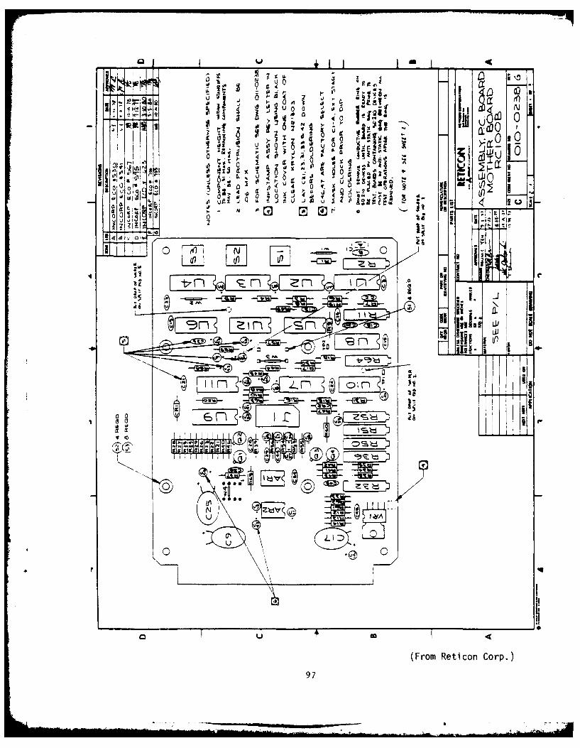
a v
4 0 0:7 U06~ 0
0 <
dl j 0 j~.~0 0 j
4 zl jo 0
H
-t7~
~-1 1f L2U-111w113
mrT~l~t, -5.
0
iI0; 0
(From Reticon Corp.)
97

7i
AD-AIIS 156 CONSTRUCTZON ENGINEERING RESEARCH LAB (ARMY) CHAMPAI F/G 1/B i3/9MICROPROCESSOR CONTROLLED WELD ARC SPECTRUM ANALYZER FOR RUALIT--ETC(U)lUN AZ 4 E NORRIS, C S GARDNER
UNCLASSIFIED CERL-TM"MN317 ML" hIIIIhIIhIubumEEEEEEEllEEllE

APPENDIX B
SCHEMATIC AND CALIBRATION PROCEDURE FOR THE ADAC 1012 A/D CONVERTER
99

- ' ;5 -";F.
-4 . .. ' o .....
l.
# S.
I - -.Z 6 , I 0 , !
ass,', ,a TT
(From ADAC Corp.)
, -. .. .., - - " . . ,
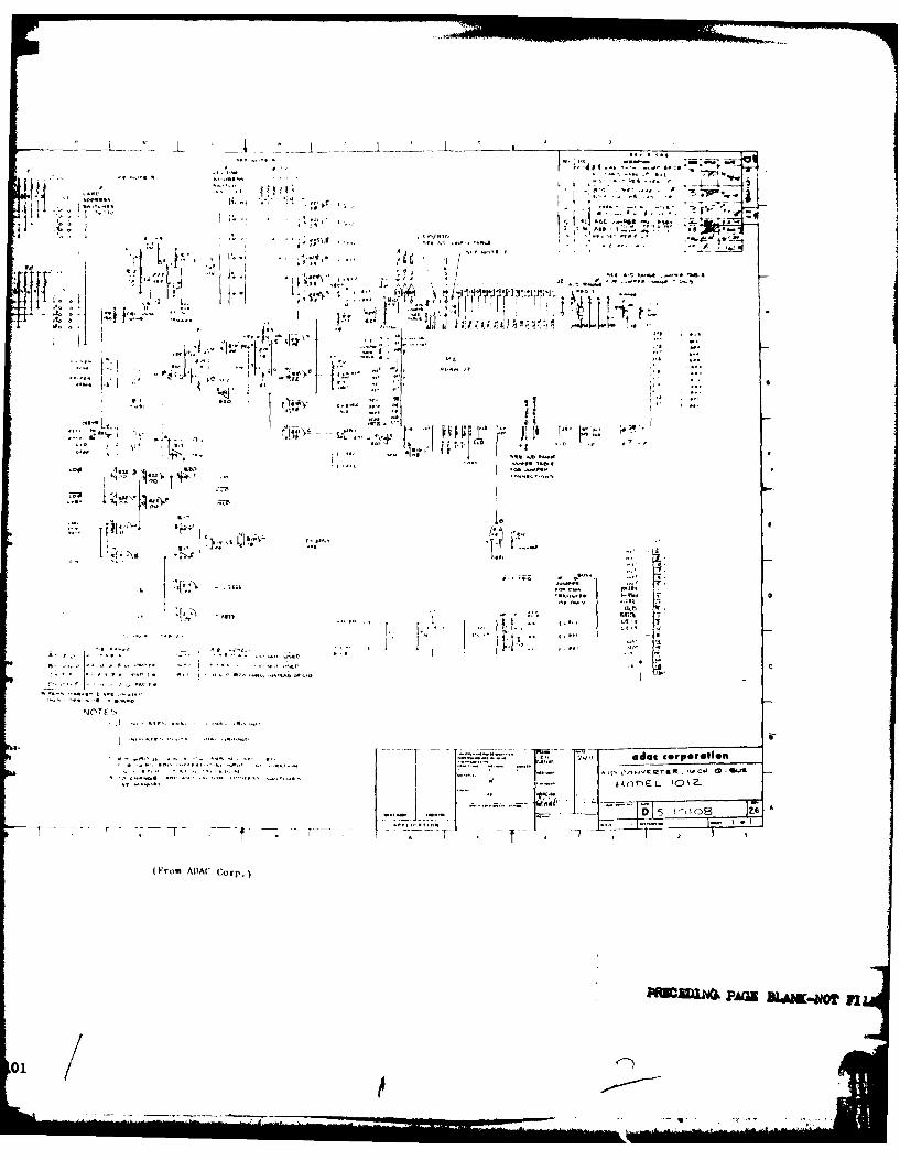
- ... ;,, .'- .-4 ,........ -- - 5,- - .
- - -:i D , 108
4 . ... - . . °'s1... ... .. 3 .,4:
. .. .,. .... .......
, -'I....
* . ;4. *' , ... ,,.,,'-. ° : ... ..
't{;h. o I I, ... '" '
, .'4L5 - .... -
1'PA 'B 4 W5W
01 ..
I A.,4 55 *.5
. ± . _ '. ,,..'.1

CALIBRATION PROCEDURE FOR THE ADAC 1012 A/D CONVERTER
1) Offset Adjustment
With the A/D board in the backplane of the LSI-ll, apply the precise
voltage shown below to any channel according to the range that has been
jumpered on the board. Force a conversion through ODT and open the output
buffer. The buffer should contain the code shown below. If not, adjust
the Offset until the least significant bit of the code alternates between
1 and 0.
RANGE INPUT CODE
-10 V to + 10 V +9.9976 V
0 V to + 10 V +0.0012 V 000000/1 UNIPOLAR
- 5 V to + 5 V -4.9988 V 004000/1 BIPOLAR
0 V to + 5 V +0.0006 V
2) Range Adjustment
After the Offset has been adjusted, the range may be adjusted.
Follow the same procedure outlined above, except this time use the values
given below and make adjustments with the Range pot on the board.
RANGE INPUT CODE
-10 V to +10 V +9.9927 V
0 V to +10 V +9.9963 V 7776/7 UNIPOLAR
- 5 V to + 5 V +4.9963 V 3776/7 BIPOLAR
0 V to + 5 V +4.9982 V
103

APPENDIX C
SCHEMATICS FOR THE ADAC 1620 DMA
105

.44.L 4
tno..
FESS
'4' 1
C1.
1154
fie-08~ r~ a o.
IL a-,CM
C.7 ---30 "-
IUD ?42 A'AL
1077
5 5 4 O N Lj.: : z . *

ILI0
" t + I J t l
-S -
7
--335 ----
B. ..JOt, " "
l
IC .8
4 4
A~m ^%:E 0-
10 7 2_

*~*~4* 1.
a,., F K0is zz
2fr -n~ r-, N.
1095

L 1I I ' 1 ' I _ , ...
1-.- e:4,- -- -- 1
! .4.. [ !, . ....
243 i "
L -
F 1- I-,S * Pill
Rs.5
' : :K -'4, 4' 4.' '4 4*' .... 14, ,
-, -4 - --- -- --
, r,,,,
-- ,J f'" U'3
,. . . .. . . .... It , ..,. .. - 2 j,, S_4o 3 ;4 f{- '
,* -.- ,. , * * *. *:::• ... - ...- " '

APPENDIX D
THE MACRO PROGRAM FOR THE WQM
sold
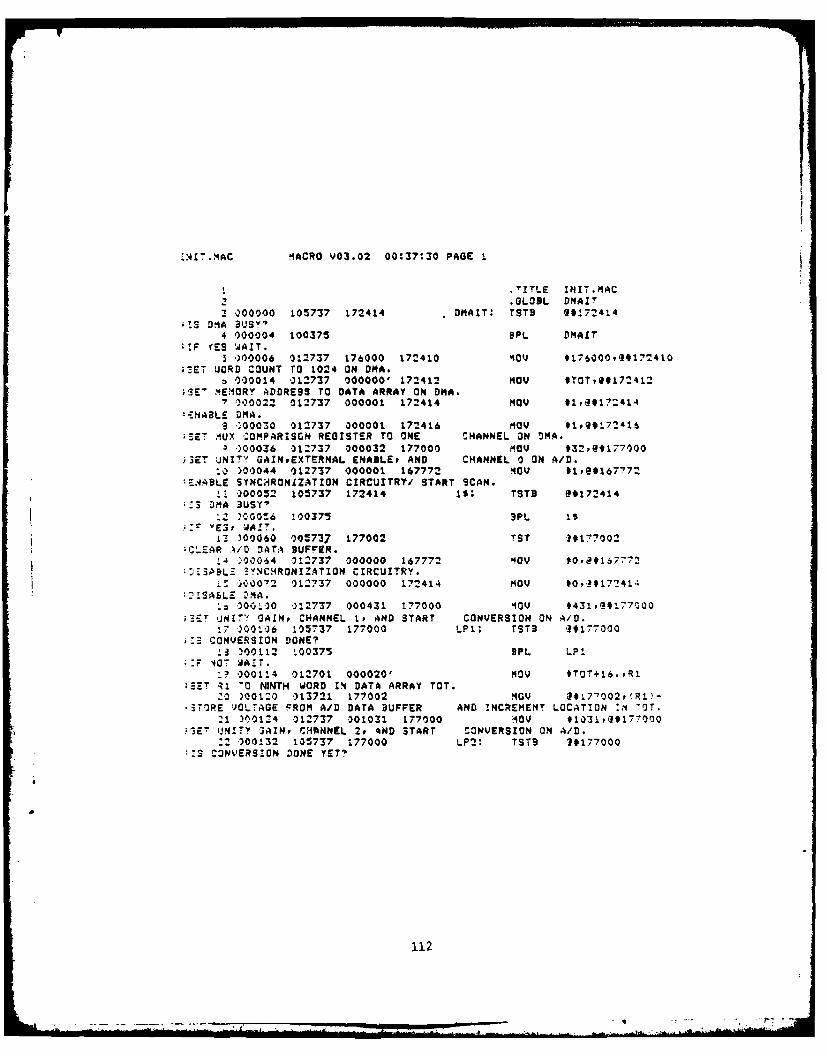
t.Z.MAC 4ACRO V03.02 00:37:30 PAGE I
.TITLE INIT.MAC
.GLOBL DNAIT1 000000 105737 172414 DNAIT: TSTB @91724±4
;S DSA BUSY"4 000004 100375 BPL DNAIT
::F YES WAIT.3 200006 012737 176000 172410 4OV t176000917:410
;3ET UCRD COUNT TO 1024 ON DNA.* 000014 012737 000000' 172412 NOV $TOT,OOL72412
;SET
MEMORY ADDRESS TO DATA ARRAY ON DMA.7-'00022 012737 000001 172414 MOV #lr4*1?:414
:.NABLE DMA.3 -00030 012737 000001 172416 NOV #I,9#172'16
;ZET7 AUX -OMPARISGN REGISTER TO ONE CHANNEL ON 3MA.
. 000036 -3:737 000032 177000 NOV t32,0*177000,jET UNITY GAINiEXTERNAL ENABLEP AND CHANNEL 0 ON A/D.
tO )00044 012737 000001 167772 NOV ttQ@167772%EABLE SYNCARONIZATION CIRCUITRY/ START SCAN.
!! 000052 105737 172414 1: TSTD %0172414::S DMA 3USY"
!2 )000!6 !003715 9PL i$VE3Y WAIT.IT )00060 005737 177002 TST 1177002
:CL AR ./D DATA BUFFER.-00064 7!2737 000000 167772 NOV #0.@0167771
:D13L3 SYNCHRONIZATION CIRCUITRY.200072 012737 000000 172414 NOv t0,59172414
:DSAL DMA.:z '200.20 212737 000431 177000 1OV t431,69177Q00
;IST QJNITY GAIN, CHANNEL 1 AND START CONVERSION ON A/D.!7 )001.06 105737 177000 LPU' TSTS 4#177000
.m5 CONVERSION DONE?: )00112 L00375 BPL LPI
*T ' 407 WAIT.'? 000114 012701 000020' NOV #TCT+16.,R$
2 3!r R1 0( NINTH WORD 1N DATA ARRAY TOT.20 )001'0 013721 177002 NGV 24177002, Rl)
o
• iTIRE UOLTAGE FROM A/D DATA BUFFER AND INCREMENT LOCATION :m 7OT.2! )00124 012737 001031 177000 NOV 01031,@17'7000
E UNITY 3AIN, CHANNEL 2p AND 3TART CONVERSION ON ./D.:2 000!32 105737 177000 LPO: TSTS 19177000
! 23 CONVERSION DONE YET'
112
__ _ _ __ _ _ . -.

23 000136 100375 BPL LP2;:F aOT JAIT.
24 000140 013721 177002 NOV 24177002pR1)+;STORE CURRENT FROM A/D DATA BUFFER AND INCREMENT LOCATION 1N TOT.
2S 000144. 012737 001431 177000 NOV 01431E$177000;SET UNITY 0AIN, CHANNEL 3t AND START CONVERSION ON A/D.
:6 000152 105737 177000 LP3: Tc-TB 0*177000;7S CONVERSION DONE YET?
-7 000156 100375 BPL LP3;:F NOT, WAIT.
23 000SO 013711 177002 mOv T*177002,R1;STORE TRAVEL SPEED FROM A/D DATA BUFFER INTO TOT.
29 )00164 000207 ENDI: RTS PC;RETURN FROM SUBROUTINE.
30 )00000 .PSECT TOTPRWtDPGBLtREL*QVR ;MAKE DATA 4RRAY TOT READ/WftITE
31!:iZRECT ACCESSGLOBAL
32';ELOCATABLEtAND OVERLAYED.
33 100000 TOT: .iLKW 1024.A IRRAY.
34 000000' .END DNAIT--NO4 OF PROGRAM
:ArT.MAC MACRO V03.02 00:37:30 PAGE 1-13049OL TABLE
iM*AT7 OO0000 G LPI 000106R LP! )OO3:R000152R TOT OOOOOOR 002
iND1 )001i4R
ADS. 000000 000)00166 001
TOT 004000 002SPAORS DET ECTED! 0
',)RTUAL MEMORY UJSED4 299 WORDS 2 PAGES).'YNA"IC MEMORY AVAILABLE FOR 57 PAGES
OK:!N:T,DK:iT-DK:INIT
113

APPENDIX E
THE FORTRAN PROGRAM FOR THE WQM
115

ZORTRAN IV V02.04
Z: PROGRAM AOSPECI WRITTEN SY: MICHAEL E. NORRISC 300 E.E.R.L.C UNIVERSITY OF ILLINOIS?c URBANAvILLNOIS 61801C
C AOSPEC IS A FORTRAN PROGRAM CREATED TO ACOUIREC PARAMETERS ASSOCIATED WITH WELDS. USING AC SPECTROMETER AND OTHER HARDWARE IT GATHERS
SPECTRAL AVERAGESt WELD CURRENTP VOLTAGE#C AND TRAVEL SPEED. IT WAS DEVELOPED UNDER A- CONTRACT WITH THE ARMY CORPS OF ENGINEERS,C ZONSTUCTION ENGINEERING RESEARCH LABS#- CAAMPAIGN, ILLINOIS.
C 2BLK CONTAINS THE RADIX 50 REPRESENTATION 3F THE DEVICEAND FILE SPECIFICATION. AVSCAN IS THE NUMBER OF
- SCANS TO B. AVERAGED.C
)C01 INTEGER*2 DBLK(4),AVSCAH
L3LK CONTAINS THE ASCII REPRESENTATION 3F THE FILE
C NAME TO BE STORED ON A FLOPPY DISK.
)002 BYTE LBLK(6)
- JTIME WILL BE USED TO STORE THE TIME IN TICKS.
C0)03 NTENERO4 JTIME
C
C IA DILL 3ERE AS AN ACCUULATOR FOR AVERAGING SPECTRAL SCANS
C0004 DIMENSION NA(1024)
c IONAN CONTAINS THE RADIX 50 REPRESENTATION OFC THE DISK DEVICE HANDLER.
005 DATA IDNAM/2RDY/CC SET UP DEVICE AND FILE SPECIFICATION IN RADIX 50.
116
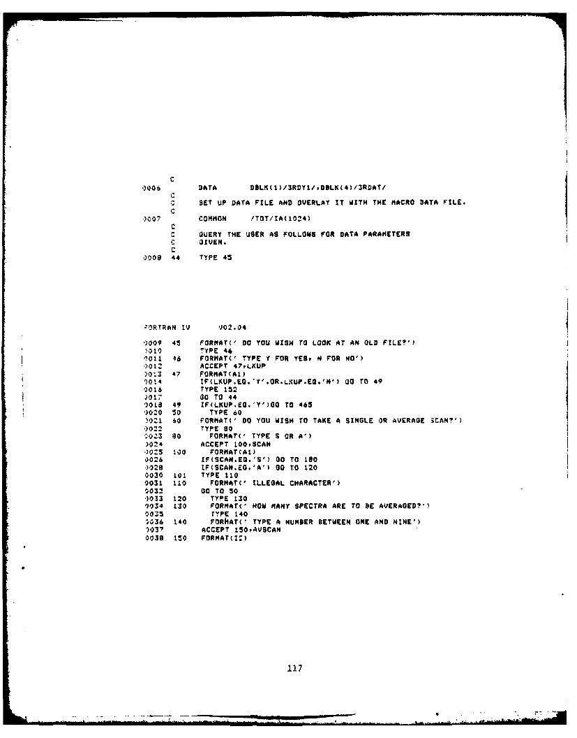
0006 DATA DBLK(1)/3RDYI/,D9LK(4)/3RDAT/Cc SET UP DATA FILE AND OVERLAY IT WITH THE MACRO DATA FILE.C
)07 COMMON !TOT/IA(1024)CC QUERY THE USER AS FOLLOWS FOR DATA PARAMETERSC 3IVEN.C
0009 44 TYPE 45
:IRTRAN IV J02.04
1009 45 FORMAT(' DO YOU WISH TO LOOK AT AN OLD FILE?'))010 !'YPE 44'0011 46 FORMAT(' TYPE Y FOR YESP 0 FOR NO')0012 ACCEPT 47,LKUP)013 47 FORMAT(A1)0014 IFlLKUP.EO.'Y'.OR.LKUP.EG.'H') GO TO 490016 TYPE 152)0i7 s0 TO 44001 49 IF(LKUP.EO.'Y')O0 TO 4659020 50 TYPE 6O)021 60 FORMAT(' DO YOU WISH TO TAKE A SINGLE OR AVERAGE 3CAN')
0022 TYPE 90O023 80 FORMAT(' TYPE S OR A'))024 ACCEPT IO0,SCAN')025 100 FORMATCA1)0026 IF(SCAN.EG.'S') O0 TO 180-)028 tF(SCAN.EG.'A') GO TO 120
0030 10i TYPE 1100031 110 FORMAT(' ILLEGAL CHARACTER')
0032 00 TO 50.)033 120 TYPE 1309034 130 FORMAT(, NOW MANY SPECTRA ARE TO 9E AVERAGED?')00,5 TYPE 1405036 140 FORkAT(' TYPE A NUMBER BETWEEN ONE AND NINE'))037 ACCEPT 150,AVSCAN0038 150 FORMAT(II)
117
- -________________________________- -

0039 IF(AVSCAN.LT.9.AND.AVSCAN.GT.0) 30 TO 1510041 TYPE 1520042 152 FORMAT(' INVALID CHARACTERS.')J043 Go TO 1200044 151 TYPE 155)045 155 FORMAT(' HOW MANY SCANS ARE TO BE TAKEN?')1046 TYPE 157.)047 157 FORMATV" TYPE UP TO A THREE DIGIT NUMBER.')0048 ACCEPT 136,IDLONO0049 IF(IBLONO.GT.O.AND.IRLONO.LT.200) 0O TO 158.051 TYPE 152)052 GO TO 151
C ADJUST rBLONO TO REFLECT BLOCKS RATHER THAN SCANS.C
)053 15 IDLONO-IBLONO*40054 156 PORMAT(13)1)055 TYPE 160105 L60 FORMAT(' ENTER A SIX CHARACTER FILE NAME HERE:')01!.'7 ACCEPT 170,(LBLK(J),J"I,&))059 170 FORMAT(6A1)
C CONVERT FILE NAME FROM ASCII TO RADIX 50 AND PLACE INc DEVICE AMD FILE SPECIFICATION.C
J059 CALL IRA0SO(6#LBLK*DBLK(2))
OBTAIN FLOPPY DISK HANDLER AND CHECK FO'? AN ERROR.
FORTRAN ZV V02.04
C
3060 IF(IFETCH(IDNAN) .HE. 0) STOP "FETCH ERROR'
C ALLOCATE A CHANNEL FOR DATA TRANSFER FROM HARD
C MEMORY TO FLOPPY DISK AND CHECK FOR AN ERROR.
2062 ICHAN-IGETC()O0&3 IF(ICHAN.LT.0) STOP 'CHMNNEL ERRI'
118

C aET THE FLOPPY DISK AREAP READY IT FOR WRITINGoC AND CHECK FOR AN ERROR.C
0065 IF(IENTER(ICHAN9D3LKoO) .LT. 0) STOP 'ENTER ERR'3067 174 TYPE 1750)69 175 FORMAT(' AT THIS TIME THE SYSTEN IS READY')0069 TYPE 1760070 176 FORMAT(' TYPE R TO START RUN OR A TO ABORT.')
C- DISABLE KEYBOARD INTERRUPT UNTIL DATA TRANSFERC HAS BEEN MADE.C
0071 CALL IPOKE('44#10100.OR.IPEEKW44))
C RESET BLOCK COUNTER.
0072 201 KLOG=O0073 202 ACCEPT 177PKEY)074 17' FORMAT(Al)0075 179 IF(KEY.EQ.'R') GO TO 300•3077 IF (KEY .EQ. 'A') 60 TO 590007? 0O TO 202
CC RESET THE DATA BUFFER.
0080 300 00 299 Ka1,10241081 29P NA(K)=O
c CONDUCT AVSCAN NUMBER OF SCANS SUCCESSIVELYC ADDING THE DATA IN ARRAY NA.
0092 30 302 JulpAVSCAN
C'ALL MACRO SUBROUTINE TO INITIATE SPECTRAL SCAN ANDACQUISITION OF VOLTAGEP CURRENTP AND TRAVEL SPEED.
0803 CALL OMAITC
C ADD SUCCESSIVE SCANS.C
0084 DO 301 1-7,10240085 301 NA(I)*NA(I)+IA(r)0086 302 CONTINUE
CC GET TINE IN TICKS PAST .IDNIGHT.
119
-t .. ...

F3RTRAN IV V02.04
C0087 CALL BTIN(JTIME)
CC CONVERT THE TICKS FOUND ABOVE INTO HOURS, SINUTES,C SECONDS# AND TICKS.C
0098 CALL CVTTIM(JTIENA(4),NA(5)NA(&),HA(8))Cc STORE THREE INTEGER VALUES CORRESPONDING TO THE
MONTH, DAY, AND YEAR.
0099 CALL IDATE(NA(1)pNA(2),NA(3))
C STORE NUMBER OF SCANS AVERAGED.C
0090 NA(7) AUSCAMC
c wRirc THE DATA ONTO THE FLOPPY DISK. IF AN ERROR
C OCCURS# REPORT IT.C
)091 IF(;WRITW(1024,NAKLOSICHAN).LT.O)STOP 'WRITE ERRI'CC ADVANCE BLOCK NUNER BY FOUR OR 1024 WORDS.C
'093 KLOG*KLOO+4
C CHECK TO SEE IF THE NUNBER OF SCANS TAKEN (KLOG)C EQUALS THE NUNBER DESIRED TO BE AGUIRED (IBLONO).C
-094 !F(KLO. GE.IBLONO)GO TO 4000096 00 TO 300
CC THE FOLLOWING CODE IS USED FOR CALIBRATION OF AC SINGLE SCAN.
C TAKE A SCAN.C
)097 190 CALL' DMAIT0093 O0 215 I-t,1024
120

CC CONVERT THE A/D VALUE TO ITS CORRESPONDING DECIMAL
VALUE.
.390 215 IA(I)s((4095-IA(I))+1)34.88
C TYPE OUT A SINGLE SCAN.C
11i00 DO 220 I-O,1016PS0101 220 TYPE $t(IA(I J)iJ1l6)0102 00 TO 590
CC CLOSE OUT THE CHANNEL AND CLEAR THE BLOCK COUNTC
0103 400 CALL CLOSEC(ICHAN)
FORTRAN rv V02.04
C RESTORE TERMINAL INTERRUPTS.
0104 CALL IPOKE(6449'167677 .AND. IPEEK('44))r)1O5 405 TYPE 4100106 410 FORMAT(' DO YOU WISH TO SEE THE RESULTS?')0!0'? ACCEPT 420,IANS0109 420 FORMAT(A1)
!F(IANS.E9.'Y'.OR.1ANSoEG.'N') GO TO 4210121 TYPE 152.1.. GO TO 405O113 421 IF(IANS.EG.'Y')GO TO 4650115 00 TO 5613116 465 TYPE 4700117 470 FORMAT(' WHAT FILE CODE WORD DO YOU YOU WISH TO ACCESS?')
0118 TYPE 4800119 460 rORHAT(' TYPE SIX CHARACTER CODE')
01"0 ACCEPT 490,(LDLK(I)r,1,6)0i :ZL 490 =ORMAT(6Ai)0122 465 TYPE fI10123 481 FORMAT(' TYPE A THREE DIGIT SCAN NUNDER')0124 ACCEPT 491,KLOO
4
121
Now---i
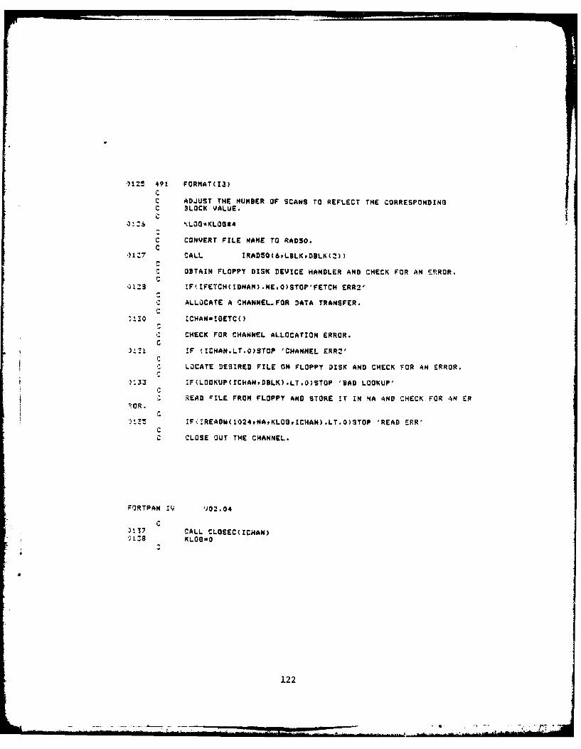
')IZ 491 FORMAT(I3)
CC ADJUST THE NUMBER OF SCANS TO REFLECT THE CORRESPONDINGC BLOCK VALUE.C
oiZs XLOG-KLOG*4
C CONVERT FILE NAME TO RADSO.C
117 CALL IRAD5O(6,LBLK,DLK(2))CC OBTAIN FLOPPY DISK DEVICE HANDLER AND CHECK FOR AN ERROR.C
0123 IF'tFETCH(IDNAM).NEO)STOP'FETCH ERR2'
C ALLOCATE A CHANNEL.FOR DATA TRANSFER.
.3O )CHANM-GETCo)
CHECK FOR CHANNEL ALLOCATION ERROR.C
")-l IF (ICHAN.LT.O)STOP 'CHANNEL ERR2'C
LOCATE DESIRED FILE ON FLOPPY DISK AND CHECK FOR AN ERROR.c
):33 IF(LOOKUP(rCHANDULK).LT.O)STOP "BAD LOOKUP'
OR. READ FILE FROM FLOPPY AND STORE IT IN NA AND CHECK FOR AN ER
iF(READW(LO24,NAKLOOICHAN),LT.O)STOP 'READ ERR'
CLOSE OUT THE CHANNEL.
FORTPAN IV 'J02.04
C3137 CALL CLOSEC(ICHAN)1ZS KLOG-O
122

PRINT OUT THE DATA READ FROM THE FLOPPY,C
'YPE 520p(LBLK(r),I=l6)0!40 520 FORNAT(*' FLENANE:',6AL)0141 TYPE 530,NA(1),NA(2),NA(3)3142 530 FORMAT(' DATE!',I2,' -',2,' -',I2)3143 TYPE S40,NA(4),NA(5)pNA(6)yNA(B)0144 540 FORMAT(, TINEelI2,' :', 2,' :',Z2," :',Z2)
C
c CONVERT SPECTRAL BINARY VALUES TC CORRESPONDINGC DECIMAL VALUES.C
.)145 DO 547,I-12,10240146 547 NA(l)-((4095-(NA(I)/NA(7)))41)E4.88')i47 30 546 19,l* 148 548 NA(I)w((NA(I)/NA(7))4A)Z4.8W
C CONVERT VOLTAGE,CURRENT, AND TRAVEL SPEEDC BINARY VALUES TO CORREUPO'lDrNG DECIMAL VALUESC AND PRINT THE DATA.C
TYPE IO00,NA(7)"0130 1000 FORMAT(' AVERAGE NO. OF SCANS='PI2)
TYPE I001MNA(9)3152 1001 FORHATt' VOLTAGE-15))i33 TYPE IOO2,NA(IO)314 1002 FORMAT(' CURRENTs'rI5)U125 TYPE 1003,NA(11)0156 1003 FORMAT(' TRAVEL 9PEEDm',15)01Z7 TYPE 4,(NA(I),Iu12v16)01138 DO 550 1*16#1016,801!9 350 TPE Sp (NA<r J),Js ,8)
C
c OUERY THE USER ABOUT THE COURSE OF ACTIONC TO BE TAKEN AS FOLLOWS:C
0160 551 TYPE 51550161 555 FORMAT(' DO YOU WISH TO SEE ANOTHER SCAN?')0162 TYPE 5560163 556 FORMAT(' TYPE Y FOR YES, N FOR NO')0164 ACCEPT 557tKAN60165 557 FORMAT(A1)0166 IF(KAMS.EG.'Y'.OR.KANS.V3.*4') 3O TO S590168 TYPE 1520169 30 To 5510170 559 IF(KANS.EO.'Y')OG TO 485)172 561 TYPE 560
123
__ _ _ _ _ __ _ _ _ _ _ __ _ _ _ _ _ __ _ _I-*
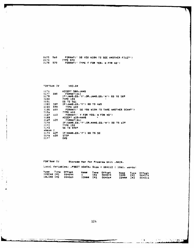
0173 560 FORNAT(' O0 YOU ZISH TO SEE ANOTHER FILE?')0174 TYPE 570'i75 570 FORMAT(' TYPE Y FOR YES, N FnR NO')
-ORTRAN rV V02.04
,)175 ACCEPT 580,JANS.17'7 50 FORNAT(A1)03179 1F(JANS.EQ.'Y'.OR.JANS.EQ.'N') 00 TO 589)130 TYPE 152-)1131 GO To 561.:92 !89 IF(JANS.EO.'Y') 00 TO 465-3194 !90 TYPE 600)185 600 FORMAT(' DO YOU WISH TO TAKE ANOTHER SCANT')1,30 T YPE 610)187 510 FORMAT(' Y FOR YES, N FOR NO')-)18a ACCEPT 620,NANSI189 i20 FORMAT(A1)7zg0 XF(NANS.EQ.'Y'.OR.NANS.EG.'N') 0O TO 629!1. TYPE 152
)193 S0 TO 590'
!! 24 629 !F NANS.EO.'Y') 0O TO 500106 630 STOP0i97 END
FOR-RAN rv Storage Nap for Program Unit .MAIN.
'zeal Oariables, .PSECT $DATA* Size -004112 C 1061. words)
4,aw T'* & Offfset Name Tpe Offset Name Tpe OffstYSCAN 102 004044 1 132 004074 IANS I12 004076
ISLONO 1*2 004060 ICHAN 1*2 004064 IDNAM :*2 00401
124
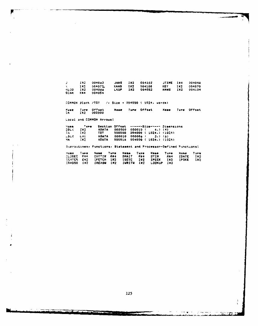
- L12 004062 JANS I$2 004102 JTZNE 1*4 004046
1*2 004072. KANS IS2 004100 KEY 182 004070LOG 1*2 004066 LKUP 1*2 004052 NANS 1*2 004104
SCAN R*4 004054
ZOMMON 3lock /TOT /v Size 004000 ( 1024. words)
aa* Tyve Offset Nee Twpe Offset Ham Twpe OffsetIA 112 000000
-oca1 and COMMON Atrrev:
l4ael Tvpq Section Offset ------ Size .--- Omensions3?L.( 122 $DATA 000000 000010 ( 4.) (4)
!92 TOT 000000 004000 ( 1024.) (1024)..5L. L-91 $DATA 000010 000006 ( 3.) (6)4A 12 $OATA 000016 004000 ( 1024.) (1024)
i3oroutines, Fqnctionst Statement and Proc*ssop-Oftined nctio 0st
see Tip. Name Tvp* Memo Twpe mnmm Tpe &I%e TiAt'SEC 9*4 CVTTIN R*4 ODAZT R*4 STIM R*4 ZDATE 182
!4TE 2 ;FETCH 1*2 ETC 1*2 IPEEK 1*2 tPOKE 1*2
!RADSO [2 rREAO 192 1wRt1? Z*2 LOOKUP 1*2
125
blow-

APPENDIX F
AN EXAMPLE OF THE DATA OBTAINED FROM THE WQMWHEN DISPLAYED ON THE DECWRITER LA-120
127
- - A-4,-
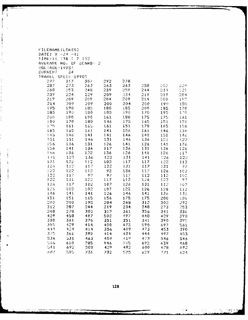
F I LENAME . LSRSS2DATE: 9 - , -'231IIME16 "18 7 :12AVE.RAGE NO. OF SCANS- 2VOL. AGE: 1905:.CURREN TT RAVE.L SFE_!:- 19905
297 317 30/ 292 278287 273 .263 263 263 258 252268 2 5 3 248 239 244 2 .2..4239 22A 229 209 )34 219 219 '4
2, 19 209 209 204 209 214 200 1
214 209 209 200 204 200 190 1 E)r195 190 185 180 195 200 185 170185 19,) 1)0 185 190 170 195 1.: 020 I s1o 190 161 180 175 175 161[8t 170 180 146 175 165 151 151
-7 161 165 161 151 170 165 1 56165 165 161 141 156 161 146 1:3'! A5 146 141 141 146 141 151 146i51 151 146 131 146 136 1".L 1221 56 136 131 126 141 126 141 1-6156 141 136 117 136 131 136 126
136 122 136 126 141 126, i11S41 122 136 122 131 141 "26 12"13 1 1'22 112 102 117 117 122 112126 1.2 11? 122 131 117 131
.22 12? 112 92 136 -1? 1.26 IC2.122 11 97 97 117 112 112, 22 131 12 117 112 126 122 97126 .[117 102 107 126 131 112 .071'. 102 102 107 1- 126 126 1 12146 141 141 126 146 141 136 1311.51 151 165 156 175 175 200 i 9Q200 200 195 204 268 312 302 292312 287 244 219 234 248 273 253268 278 302 317 361 356 341 336429 458 497 502 i97 448 429 ,70390 361 370 351 351 341 390 39'395 429 414 400 473 590 697 561'144 424 414 356 409 473 453 3903,5 366 390 114 434 444 497 4535.36 t31 463 409 i?19 473 546 546566 610 785 946 795 692 639 468541 692 580 429 4192 600 678 692
59. 736 732 575 629 1 624
128
................................... ,

.575 561 585 668 624 522 458 41943 '22 197 439 478 497 551 6537 27 683 /56 751 946 1476 1.903 1424
1.146 922 834 1029 1302 1.171. 1117 1156I000 1146 1224 1093 951 917 1019 985i 1.} 1293 !I1i5 863 727 653 629 575'85 492 4,)3 448 '144 409 463 483
70 /17 722 658 590 639 605 478173 468 468 444 473 507 502 139
7'. 308, 395 473 649 805 614q/3 414 395 375 414 409 405 390'I09 390 409 380 370 331 317 307351 375 434 683 1044 814 448 351
B 0 370 351 346 380 375 395 424419 385 39(C 356 351 2*6 322 3313e,6 385 3?'0 336 331 31/ 326 336361 33! 336 336 346 317 331 33140 ", 463 4 5 3 385 414 3 70 351 331356 375 400 336 336 326 331 302,2 322 331 326 246 322 302 28731/ 307 326 326 326 297 292 287312 32 3122 312 "26 312 32' 292326 326 3,11 341 390 390 405 4291i-.4 405 429 ,163 497 '09 390 395
46E F 473 114 356 370 351 326 302•1 - - , , -z ' 3 2 22 3 22 9.2 2 326 317 307 322 317 32 322361 351 351 361 400 414 400 36i,56 346 341 322 351 336 370 36.385 380 385 361 419 453 419 370,58 536 527 395 390 405 463 536517 400 405 414 434 400 356 312146 356 361 331 351 -26 317 317-37 307 326 322 341 312 322 - 322
336 376 341 307 356 356 341 307312 312 302 292 302 263 278 26328? 292 302 312 336 375 375 302287 287 283 297 317 283 278 283297 2,3 283 283 307 292 268 253".8 26 273 244 283 278 273 2973 3. 322 ,312 263 287 263 278 253268 273 287 278 312 278 283 26329" 273 263 244 268 258 258 239248 263 2/3 253 278 278 268 268.1. 248 244 263 258 253 244258 253 283 283 322 322 29"7 273
53 258 239 258 248 239 224
229 224 219 239 229 229 20?
129

29 214 229 214 229 224 204 209-24 224 22l9 239 283 292 27 244-.. 229 214 204 229 214 209 195209 219 209 195 219 204 200 200219 195 200 180 209 200 200221 209 195 185 214 204 195 1.p,.:04 204 209 195 204 204 204 190
209 190 180 165 190 185 !90 1.'?5200 185 190 165 200 190 175 180190 1.90 170 170 190 185 170 17517" 1.75 175 141 180 170 151 156175 161 165 151 170 175 165 146i70 161 165 146 165 170 161 146175 151 156 146 146 146 151 12156 1'6 1l 117 151 126 13 6 !22136 .1.36 141 141 146 146 141 112141 126 122 117 141 141 131 126146 it7 131 1I" 141 136 .31a 11214i. 141 146 117 156 146 131. 11714.l 97 136 107 131 122 1.26 107
"22 131 107 141 122 17 17126 131 117 117 126 117 117 102102 117 112 112 .1.22 122 17 97126 117 122 97 126 107 111/ 102'131 112 122 102 117 112 107 92117 97 126 97 126 122 107 1021.-26 112 126 102 102 107 112 1021I2 - It2 1.12 1o/ 1.17 112 101.02."22 117 97 97 117 97 102 107:1 02 107 107 97 1. 1.." 117 112 8"1 1." 97 1.02 97 :. 12 107 107 97131 97 107 92 102 102 1.12 87122 102 97 82 .!. 12 112 9?117 92 102 92 112 112 07 1 " 2
'7 97 102 78 107 11.7 92 87
112 102 1.07 97 L22 97 102 37102 97 102 97 102 102 102 78102 97 82 82 1!.2 92 102 92102 102 102 97 97 97 92 ")
112 97 5" 73 102 112 78 82107 87 97 92 112 .1.57 87
130
4 . ... ~~~ ~ S - " -

APPENDIX G
AN EXAMPLE OF CALIBRATION DATA FOR THE
SPECTROGRAPH TAKEN USING THE WQM
131 V

i N . .. .. . . . . .. . i
DO 'iOIJ W IScH 1 '0 LOOK AT oN OLD IL.E?TYPE Y F(R YES, N FOR NONDO '(OU W.[SH 1r TAKE A SINGLE OR AVERAGE SCAN?TYPE S OR As
39 43 146 161 117 97 11.2 9219573 1?602 19637 102 102 102 97 69
107 112 102 82 97 102 112 1021.02 9.' 97 92 102 122 102 102J 17 1?7 1.12 102 1.02 107 102 10"
112 112 92 97 107 97 102 92v2 97 102 102 1.02 102 122 87
102 52 '2 87 92 97 107 781. 07 87 87 .12 102 -92 82102 107 122 82 97 92 102 102122 97 87 92 102 87 ±07 c7
92 102 97 68 87 97 97 78107 10/ 82 87 117 92 97 92117 87 97 92 117 112 9,
112 97 97 102 97 97 1. 17 82
11 102 87 87 102 112 3102 92 107 102 107 97 102 82102 97 97 92 97 97 107 9-7.122 Y7 92 102 102 87 107 879,] 1.07 92 78 92 102 1.07 73
107 112 87 97 112 92 102 87112 87 92 8"7 117 112 9? 92
1")2 102 102 107 102 102 122102 1.12 97 87 87 102 117 E2102 92 102 107 117 107 102 !2102 97 102 102 107 97 102 10y
22 1.02 92 102 112 92 11-11102 112 82 97 107 11 : 92
11l i12 92 102 122 92 107 9211" 87 102 92 117 122 112 102.. 102 102 107 102 97 112 92
102 112 97 92 87 102 112 82102 97 102 97 10? 97 97107 92 92 92 102 97 107 102
122 ,7 107 1.02 87 107 2tj t 102 97 73 92 97 97 7
107 8 92 107 82 107 87
132

10, <8 92 8>' 112 112 92 92122 92.) 92 97 97 97 112 329"? 112 92 82 92 102 112 73'.02 87 107 92 112 97 97 82107 8/ 92 92 107 107 97 73102 97 97 73 107 107 87 97112 87 107 102 112 87 97 87117 112 97 102 122 97 87 971.02 87 107 92 97 107 97 73
97 102 97 73 107 107 87 97117 87 102 87 112 87 92 8,1112 112 92 92 122 92 102 102102 97 112 82 97 112 97 82102 102 112 78 102 92 102 9711 10) 102 82 102 92 97 92i1. 11?1 97 73 112 102 107 78107 107 87 97 117 87 107 107141. 87 97 92 1.17 112 102 102112 102 92 1.02 102 92 117 92
97 117 102 82 92 107 112 87'12 107 112 97 112 107 112 102-112 112 102 102 92 107 112 82112 107 97 82 97 102 122 10?112 1.02 117 87 1.12 117 97 92122 97 102 102 102 92 102 92
112 97 97 97 92 92 87 87112 112 97 87 B7 97 87 82112 92 112 82 97 87 92 92
92 102 102 73 102 97 97 82". ?2 102 97 92 92 92 92
97 12"2 92 97 122 87 107 97'97 i02 107 82 87 102 102, 92F;3 97 97 73 107 102 82 87
.1.2 107 82 78 97 107 112 82112 122 92 73 107 92 82 97102 87 102 82 87 87 97 92
92 112 107 73 107 107 92 97107 112 87 87 112 112 112 9211"2 112 92 87 122 97 102 1029'/ 92 112 87 97 92 102 102
102 97 92 92 122 112 102 92102 92 97 92 112 97 97 9212'2 122 9? 78 112 102 87 92112 87 102 97 97 87 112 102102 112 112 82 117 117 92 102107 112 87 97 11.2 11 122 9211; 122 102 92 122 102 102 107
133
- - - -,. ...,
... .. ' ... ...... ... " .... '± .. . . ... ' - , ," .,' ;. 2 2 ,..

122 87 97 97 117 112,02 f.2 97 102 122 107 102 97ii2 102 92 87 112 97 97 97122 122 102 78 112 97 82 87
2 82 102 92 82 87 97 9787 102 112 73 112 112 82 97
107 11.2 82 87 107 112 112 87112 112 97 87 122 97 97 102102 92 112 87 97 87 107 10292 97 87 97 107 107 92 02
I0.! 97 87 87 107 102 122 8792 107 102 97 92 107 112 73
112 112 92 97 122 97 92 a7i0/ 112 122 92 117 122 97 73112 97 87 92 102 87 102 9787 8/ 102 92 87 107 107 73
107 107 82 87 97 107 '7 0i02 107 12"2 92 112 112 92 78112 92 92 102 97 92 112 8297 87 102 102 97 92 92
117 1.07 97 92 87 102 87 87112 87 97 92 122 122 97 82IL7 97 87 97 J07 87 102 82,. 92 102 92 87 102 107 73
112 107 82 97 112 112 87 92
107 97 97 92 97 92 ?7 1029'7 107 97 102 112 92 97 87
112 97 102 87 122 122 102 102112 102 112 102 102 87 102 92112 87 97 97 87 97 107 78
107 97 68 92 102 107 97i12 112 97 92 97 1.17 97 78112 9? 87 97 102 87 87 87
107 87 97 92 92 102 97 73107 107 97 68 97 97 107 97i12 971 112 78 107 117 97 92122 97 102 102 107 92 102 97117 92 102 87 112 112 112 87112 92 9) 82 102 112 107 107102 87 1.02 92 117 9 102 107
92 :107 107 78 112 11' 112 8210? 102 1 t' 97 107 1. .2 1 2 8792 312 97 82 1.17 97 92 92
112 92 87 92 112 87 107 102
134
M~6

APPENDIX H
FLOPPY DISK FORMATTING AND INITIALIZATION
Inherent in the RT-11 System Software is a utility program called
"Format." Any new floppy disk will be unformatted (note: formatting
destroys data currently on a disk). To format a floppy disk for this
system, type in on the LA-120, "R FORMAT." Then press the return button.
The utility program will respond with a prompt that looks like this: *.
Then, assuming the unformatted disk is in slot 1 and the system floppy
disk is in slot 0, type "DYl:/Y." Then press return.
To initialize the floppy disk for file structuring (this will also
destroy all existing files on the floppy disk), type in: "INITIALIZE/
BADBLOCKS DYI:." The system will respond with: "DYl: Init are you
sure?." Type in "Y." The floppy disk will now be ready for data
accumulation. Further information on these commands can be found in the
RT-11 operator manuals.
135
iiiiiiiiiiiiiiijil

REFERENCES
[1] F. Kearney, "Nondestructive testing for field welds: Real timeweld quality monitor," CERL Rep. M-251, August 1978.
[2] F. Kearney, "Optoelectronic weld evaluation," ILIR Report-FY1976 work.
[3] R. Weber, F. Kearney and S. Joshi, "Development of a weld quality
monitor," CERL Rep. M-183, July 1976.
[4] Dolan-Jenner, Bulletin 878, "High temperature fiber optics,"Revised February 12, 1978.
[5] DEC Microcomputer Processor Handbook, published by Digital EquipmentCorporation, 1979.
[6] DEC Microcomputer Interfaces Handbook, published by Digital EquipmentCorporation, 1981.
[7] MDB MLSI-DRVIIC Parallel Line Interface Module Instruction Manual,published by MDB Systems Inc., 1978.
[8] RT-11 Operator Manuals, published by Digital Equipment Corporation.
[9] ADAC Instruction Manuals, Models 1012, 1014, 1012EY, and 1620DMA,
Data Acquisition Systems Compatible with DEC LSI-11 and LSI-lI/2,published by ADAC Corporation.
[10] DEC LA120 User Guide, published by Digital Equipment Corporation,1979.
136
I . . ....... . ... ....,- .. _ , ....... .L_ , " ' ... . .. .i ... .---- ,.---~ J '

Chief of Lt'iner. Oth USA, , rta IN0019 - Ch 1.n9tL. Div.ATTN: Tech Mlitur ATTN: LAPE 19) 08301 ATTN: Facilities EngineerATT4: 0ALN-AS-t t2) ATTN; EAFEY 986388 ArLington MelL Station 12) 2ATTN: OAEN-CCP ATTN: FE9-10 91224 Vint HILL Fere Station 2MIATTN: 0AN-CW A"Th: AF26-401 99208ATTN: DAEN-CWE ATTN: EAFE-H 6271 999ATTN: DAE-CYWi-F ATTN: AFE-P 99289 ATTN: Fo1Liltio EngineerATTN: UAEN-CsiC ATTN: LAFF-T 99212 Cameron Station 22314ATTN; DAEN-09P Fort LasLey J. Mlcair 20319ATTN: OAEN -P Hooky Mt. Arasnal., 8 W-IS 500022 Fort Myer 22211ATTN: OAEN-MiCATl.t: OAEN-iPE Arte Enineaer. ASIC-Area Office NTMCAiTN: 2AEN-MPO Arnol1 Air Force Station, TN 37309 ATT : KTNC-SA 20315ATTN: DAEN-MPR-A ATi, Facilities EnginerATTN: 0AEN-) Weatarn Area ffice, CE Oakland Army e@* 94922ATTN: DAIl-AOL Ardarberd AFB, CA 93437 Sayonne 9O1 07002ATTN: cAEN-ROM Sunny Point NOT 28461ATTN: DAEN-AM 410th Engineer Commend 6002JATT: 0AEN-Z ATTN: Foi i ar .a .I 2ARADCO . ATN: DRDNA-F 071160ATTN: DAEN ZCEATTN: OAN-ZOl USA Japan :USARJI TARCO , Fec. Div. 4900ATTN: DAEN-ZM Ch, FE Uiv, A.JEi-cE 9343
Foc Engr (Honahu) 96343 TECOM. ATTN: ORtTE-L--F 21006fLSA ATTN: 'rorer
0 22060 P., Er-gr lOknowa) 96331
TRADDCFESA, ATTN: 01t ILL 79Sft ROK/U CoclneC Forces Command 16301 HO, TRADOC, ATTN; ATEN-FE
ATTN: FUFA-HHC-CFCEngr ATTN: FaciLities Engineer016 Army Engineer Dionricta Fort Bslnoir 22G60
ArTN: lirry US Militery Aado, 1096 Fort Banning 31805ALoBk& ,iS01 ATTN: Folitlio Ergiseer Fort OLil. 79916AL dtrn U961, A-TN: Oept of GeogroOhy & Carlisla Barracks 17013ALbuqurque H7103 Cornuter Science Fort Chaffee 72902213liner, 21203 A i": FSCPER/MAEN-A Fort 0i 08640Buffo 14207 Fort Eustis 23804ChorleSt :: '9402 Engr. Stoules Cantor 20315 Fort Gordon 30905crcy 62604 ATO: Lilrr-, Fort Hemilton 11252Dntroit 4A,31 Fort Aenj wln Harrison 45iFar East 90301 1AM , ATTN: DAXMF-WE 12172 Fort Jackan 29207Fort Wrtn 751D? Fort Kne, 40121GOlunate,: 77550 -SA AhRCOr 6'g8 Fort Leanaortr 5027HuntrO'teOg 2571 ATTN RCHS-Hj-1 Fort Lee 23801Joa-SOtl l 32232 ATTN: 2PSAR-Lb Fort MCltLon 3620Jopo 91343 Fort nrn o 23651Kaena L~t 64106 3ARCO2 - ir., ,nat., & SCS. Fort Rucker 36362little Alea 72203 ATTN: Faclitie Egnaar Fort iL 73503Lo Anql era 90053 AHRADC2 :7601 Fort Leonard Woad 65473LO.AUlrav 40201 Aberdeen Proving Ground 21005MHapri 39103 Army Motl. od Mechanics Res. Cir. TSARCOM. AiTN: STSAS-F 53120MoHe 3620 Lurpue Chriati Army Depot 78418N901 Lin 3720P Harry Oiswond Laboratories 20723 uSACCNtw Orters 70160 Ougwey Proving Gound 84022 ATTN: Falitis Engineories 00,k 1 01J07 Jefferson Proving Ground 47250 cart Hutchuce 65613Norfet '3510 Foro Moncooth 07703 romt Raonu 21719Denoc 6102 Lettarkenny Army Depot 17201Phltadelpnrl 19106 Natick RD Ctr. 01780 MESTO MPitbor1 15222 Ne. Cuorlnnd Army Depot 17070 ATTN: Failitio EnginssrPnaorrd 97P08 Pueblo Amy Oept 01001 Fort Shtfter 96658Tyod" 11035 Ra' Rioar ARmy Depot 75501
qc R ln:) 51201 Hastenr A1 enl 3802 SHAPE 09055
or9en5to 9514 Rok Iltnd Arsenal 61228 ATTN: Suroioohito Orction. PSb'r. Frln"iuo 94105 Saonno Amy epot 61074 Infrstructore Brach, LANDAovannah 31401 Shrro Army Depot 95331
FeoIttle 3614 S.e.o tray Oe: 14541 0 USEUCOM 0912S3t. Lous :'3101 Toylnno. Army input 19486 ATTN: ECJ 4,7-LOESt. PAUl 55101
Toone" Amy Dept 4074
Tulso /4102 etervle Arsonel 12'188 For: BaLvo'r, VA 22080Virkhar' q91BU Yum Provin
g Ground 85364 ATTN: ATZA-DTE-EM
2,11" 201L 15362 Whit. Sendo MInLorl Range 99000 ATTN: ATZA-DTE-SWWInrlqtn 28401 ATTi: ATZA-FE
OLA ATTN: VLA-91 22314 ATTN: Engr. Library:$ Army Fhiner Dierainno ATTN: Canodian Lialor Office (2)311 : Lrarry FORSCOM ATTN: 1WR Library
E,.rope 09757 FORSCOM Egitone, ATTN: AFElftFE,aunt-vl"l 3580 AT7N: FociLto Engineer Cold Feona Reaearch Etinring Lob 03755Lower lasisnsa1pPi Valley 39'80 Fort 5ucnhnan 00934 ATTN: LibraryMiddlr Eant q9038 Fort Bragg 28307Middl 0 East Ilear 22601 Fort CespbelL 42223 ETL, ATTN: Library 22080MISue,, 'oar '8101 Fort Coraon 62913New England 02154 Fort Dean. 01433 eaterveya Experiment Station 3910North Atlantic 10027 Fort Drum 13601 ATTN: LibraryNorth Central 60605 FORGCOMorth P.Fa1fi 97208 ATTN: Flcilitino Engirror 6
n, XVII Airborne Corps end 28307
hino Aiver 49701 Fort tiad 76544 Ft. 9raggPacifro Ocean 96858 Fort Indlanton (lp 17003 ATTN: AFZA-FE-EESouth Atlantic 30303 Fort 1rm 52311South Pacific 94111 Fort Som Houeton 78234 Cnute AF, IL 81969Southwestern 75202 Fort Lewis B8433 3348 CES/OE, Stop 27
FOrt McCoy 5468dS Army Frope FOrt Mcaerson 30330 Norton AF 90409.0, 7th Army Training Command 09114 Fort George G. Head* 20755 ATTN: AFRCE-/DIEE
AdTI; AE-rG-DEH (5) Fort rd 893841HiO ith Amy ODCS/Engr. 09403 Fort Polk 71489 NCEL 93041
ATTN: AEAEN-EH (4) Fort RITchardon 985 ATTN: Library tCoda LO8AV. Corpm 09079 Fort Ri Lay 8442ATTN: AETVDEH (5) Presidio of San Francisco 94129 TyndLL AFB, FL 32403
A!E. Caren 09154 FOrt Sheridan 20037 AFESC/Enginesring Service LobATT: AFt0OEH 9J10 Fort Steesrt 31313aet Sipport Conaund 09325 Fort Wainwright 927013 Defense Technical Info. Center 22314ATTN: AE6H 151 Vencouver ikges.6880 AM"1, DA (121
br n 09742ATN: AERk-EN 21 l$C Engineering Societies Library 10017Gorthern European Tesk Force 08169 ATTN: HSL0F 79234 .N York, NYATTN: Ae-ENG 31 ATTN: Fecititnin Enginear
"rnt iiatii4in Support Activity 08403 Fitzsimons Army Medical Center 80240 National Ocerd Bureau 20310ATTN: A6(ES-nP Wecter Read Army Holical Center 20012 netaLLetion Divison
US Governmeet Printing Office 2804Recloving Section/opsimtory Copies (9)
262
EIMl Team Distribution
Director of Facilities Engineering US Army Engineer DivisionMiami. FL 34004 New England
ATTN: Chief, NEDED-1
West Point, NY 10996 North AtlanticATTN: Dept of Mechanics ATTN. Chief, NADEN-TATTN: Library South Atlantic
ATTN: Chief, SADEN-TSChief of Engineers HuntsvilleATTN: DAEN-MPO-U ATTN: Chief, HNDED-CSATTN: DAEN-MPZ-A ATTN: Chief, HNDED-SRATTN: DAEN-MPR Ohio RiverATTN: DAN-RDL ATTN: Chief, Engr Div
SouthwesternFort Belvoir, VA 22060 ATTN: SWDED-TMATTN: Kingmlan Bldg. Library Pacific OceanATTN: Canadian Liaison Officer (2) ATTN: Chief, Engr Div
North PacificFort Leavenworth, KS 66027 ATTN: Chief, Engr DivATTN: ATZLCA-SA
AFESC/PRTFort McPherson, GA 30330 Tyndall AFB, FL 32403ATTN: AFEN-CD
Tinker AFB, OK 73145Fort Monroe, VA 23651 2854 ABG/DEEEATTN: ATEN-AJ (3)
Patrick AFB, FL 32925USA-WES ATTN: XRQATTN: C/Structures
McClellan AFB, i.A 956526th US Army 2852 APG/OEATTN: AFKC-EN
Naval Air Systems Command7th US Army ATTN: LibraryATTN: AETTM-HRD-EHD WASH DC 20360
US Army Science & Technology Naval Facilities Engr CommandCenter - Far East Office ATTN: Code 04
Alexandria, VA 22332
US Amy Engineer DistrictPhiladelphia Port Hueneme, CA 93043
ATTN: Chief, NAPEN-D ATTN: Library (Code LO8A)Baltimore
ATTN: Chief, Engr Div Washington, DCNorfolk ATTN: Transportation Research Board
ATTN: Chief, NAOEN-D ATTN: Library of Congress (2)Wilmington ATTN: Dept of Transportation Library
ATTN: Chief, SAWEN-DCharleston National Defense Headquarters
ATTN: Chief, Engr Div Director General of ConstructionSavannah Ottawa, Ontario
ATTN: Chief, SASAS-L Canada KiA OK2Jacksonville
ATTN: Const Div Airports and Construction Services DirMobile technical Information Reference Centre
ATTN: Chief, SAMEN-C Ottawa, OntarioATTN: Chief, SAMEN-D Canada KIA ON8
MemphisATTN: Chief, LMMED-DM 64
VicksburgATTN: Chief, Engr Div
LouisvilleATTN: Chief, Engr Div
St. Pau)ATTN: Chief, ED-D
OmahaATTN: Chief, Engr Div
New OrleansATTN: Chief, LMNEO-OG
Little RockATTN: Chief, Engr Div
San FranciscoATTN: Chief, Engr Div
SacramentoATTN: Chief, SPKED-O
PortlandATTN: Chief, DB-6
SeattleATTN: Chief, MPSCO
Walla WallaATTN: Chief, Engr Div
AlaskaATTN: Chief, NPASA-R
i-.

Norris, Michael E.
MicoproceOSsor controlled Wald arc spectrum analyzer for qualityontrol and analysis. -- Champaign, LL : Construction Eniineuring
Research Laboratory ; available from NTIS, 1982.
127 p. (Technical report ; Custruction Engineering Research
Laboratory ; M-317) Thesis (M.S.) - University of llinois, 1982
I. Welded joints - detects - testing. 2. Spectrograph. 1. Title.
It. Technical manuscript (Construction Engineerin8 Research laboratory,
(U.S.)) ;M-317.

AL
Recommended