Freescale SemiconductorData Sheet: Technical Data
Document Number: MCF5271ECRev. 4, 08/2009
Contents
MCF5271 Family Configurations . . . . . . . . . . . . . . . . . . . 2Block Diagram . . . . . . . . . . . . . . . . . . . . . . . . . . . . . . . . . 2Features . . . . . . . . . . . . . . . . . . . . . . . . . . . . . . . . . . . . . 4Signal Descriptions . . . . . . . . . . . . . . . . . . . . . . . . . . . . . 4Design Recommendations . . . . . . . . . . . . . . . . . . . . . . . 8Mechanicals/Pinouts and Part Numbers . . . . . . . . . . . . 12Electrical Characteristics . . . . . . . . . . . . . . . . . . . . . . . . 17Documentation . . . . . . . . . . . . . . . . . . . . . . . . . . . . . . . 39Document Revision History . . . . . . . . . . . . . . . . . . . . . . 39
MCF5271 Integrated MicroprocessorHardware Specificationby: Microcontroller Solutions Group
The MCF5271 family is a highly integrated implementation of the ColdFire® family of reduced instruction set computing (RISC) microprocessors. This document describes pertinent features and functions of the MCF5271 family. The MCF5271 family includes the MCF5271 and MCF5270 microprocessors. The differences between these parts are summarized below in Table 1. This document is written from the perspective of the MCF5271 and unless otherwise noted, the information applies also to the MCF5270.
The MCF5271 family combines low cost with high integration on the popular version 2 ColdFire core with over 144 (Dhrystone 2.1) MIPS at 150 MHz. Positioned for applications requiring a cost-sensitive 32-bit solution, the MCF5271 family features a 10/100 Ethernet MAC and optional hardware encryption to ensure the application can be connected and protected. In addition, the MCF5271 family features an enhanced multiply accumulate unit (eMAC), large on-chip memory (64 Kbytes SRAM, 8 Kbytes configurable cache), and a 32-bit SDR SDRAM memory controller.
123456789
© Freescale Semiconductor, Inc., 2009. All rights reserved.
MCF5271 Family Configurations
1 MCF5271 Family Configurations
2 Block DiagramThe superset device in the MCF5271 family comes in a 196 mold array plastic ball grid array (MAPBGA) package. Figure 1 shows a top-level block diagram of the MCF5271.
Table 1. MCF5271 Family Configurations
Module MCF5270 MCF5271
ColdFire V2 Core with EMAC and Hardware Divide
x x
System Clock 150 MHz
Performance (Dhrystone/2.1 MIPS) 144
Instruction/Data Cache 8 Kbytes
Static RAM (SRAM) 64 Kbytes
Interrupt Controllers (INTC) 2 2
Edge Port Module (EPORT) x x
External Interface Module (EIM) x x
4-channel Direct-Memory Access (DMA) x x
SDRAM Controller x x
Fast Ethernet Controller (FEC) x x
Hardware Encryption — x
Watchdog Timer (WDT) x x
Four Periodic Interrupt Timers (PIT) x x
32-bit DMA Timers 4 4
QSPI x x
UART(s) 3 3
I2C x x
General Purpose I/O Module (GPIO) x x
JTAG - IEEE 1149.1 Test Access Port x x
Package 160 QFP,196 MAPBGA
160 QFP,196 MAPBGA
MCF5271 Integrated Microprocessor Hardware Specification, Rev. 4
Freescale Semiconductor2
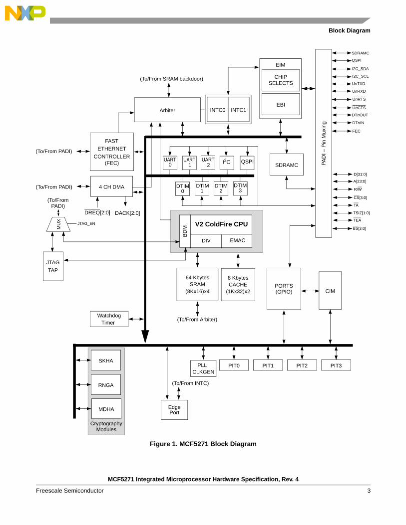
Block Diagram
Figure 1. MCF5271 Block Diagram
64 KbytesSRAM
(8Kx16)x4
EIM
ETHERNET
V2 ColdFire CPU
INTC0
Watchdog
PIT0
JTAGTAP
CACHE(1Kx32)x2
PIT1 PIT2 PIT3
4 CH DMA
UART0
UART1 I2C QSPI
DTIM0
DTIM1
DTIM2
DTIM3
TimerPA
DI –
Pin
Mux
ing
PLLCLKGEN
UART2
8 Kbytes
EdgePort
SDRAMC
CHIP
EBI
SELECTS
(To/From PADI)
(To/From
FAST
CONTROLLER(FEC)
FEC
DTnIN
DTnOUT
UnRXD
UnTXD
I2C_SDA
I2C_SCL
SDRAMC
QSPI
UnRTS
UnCTS
PORTSCIM(GPIO)
D[31:0]
A[23:0]
R/W
CS[3:0]
TA
TSIZ[1:0]
TEA
BS[3:0]
DIV EMAC
DREQ[2:0]
INTC1Arbiter
(To/From SRAM backdoor)
(To/From Arbiter)
SKHA
RNGA
MDHA
(To/From PADI)
CryptographyModules
DACK[2:0]
BD
M
(To/From INTC)
MU
X
PADI)
JTAG_EN
MCF5271 Integrated Microprocessor Hardware Specification, Rev. 4
Freescale Semiconductor 3
Features
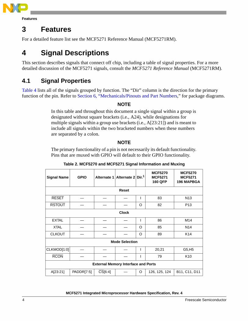
3 FeaturesFor a detailed feature list see the MCF5271 Reference Manual (MCF5271RM).
4 Signal DescriptionsThis section describes signals that connect off chip, including a table of signal properties. For a more detailed discussion of the MCF5271 signals, consult the MCF5271 Reference Manual (MCF5271RM).
4.1 Signal PropertiesTable 4 lists all of the signals grouped by function. The “Dir” column is the direction for the primary function of the pin. Refer to Section 6, “Mechanicals/Pinouts and Part Numbers,” for package diagrams.
NOTEIn this table and throughout this document a single signal within a group is designated without square brackets (i.e., A24), while designations for multiple signals within a group use brackets (i.e., A[23:21]) and is meant to include all signals within the two bracketed numbers when these numbers are separated by a colon.
NOTEThe primary functionality of a pin is not necessarily its default functionality. Pins that are muxed with GPIO will default to their GPIO functionality.
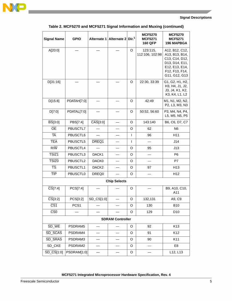
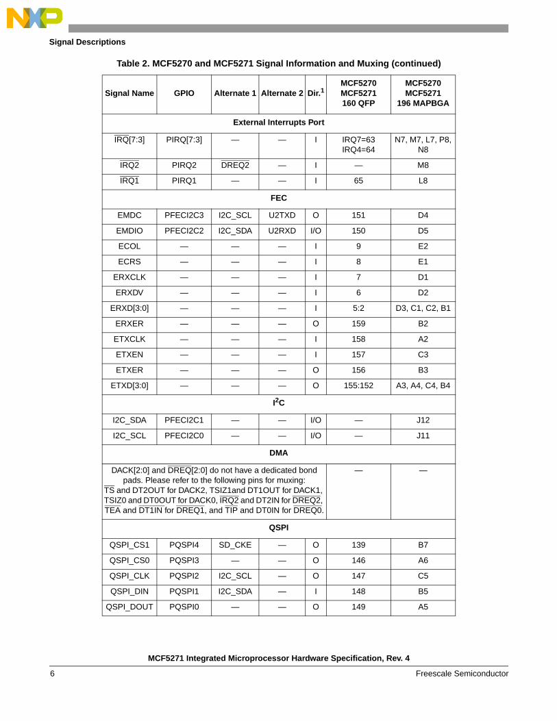
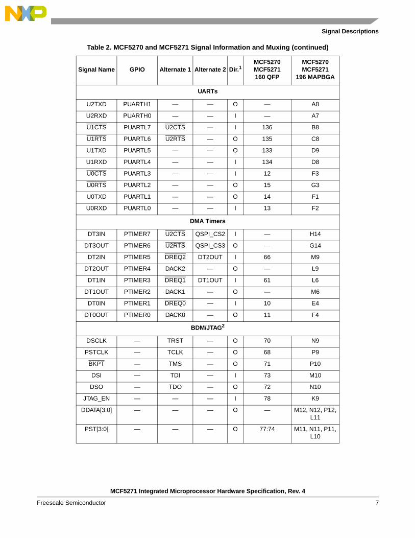
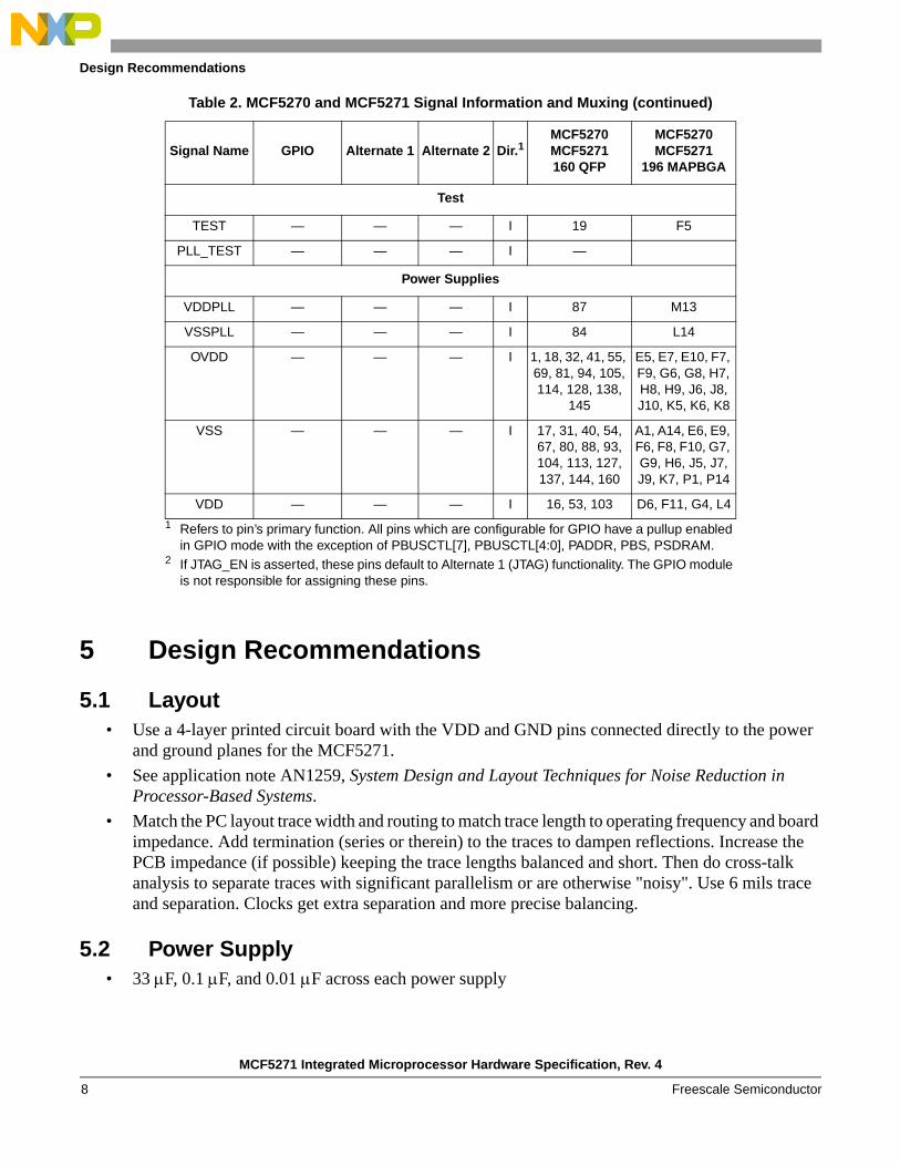
Table 2. MCF5270 and MCF5271 Signal Information and Muxing
Signal Name GPIO Alternate 1 Alternate 2 Dir.1MCF5270MCF5271160 QFP
MCF5270MCF5271
196 MAPBGA
Reset
RESET — — — I 83 N13
RSTOUT — — — O 82 P13
Clock
EXTAL — — — I 86 M14
XTAL — — — O 85 N14
CLKOUT — — — O 89 K14
Mode Selection
CLKMOD[1:0] — — — I 20,21 G5,H5
RCON — — — I 79 K10
External Memory Interface and Ports
A[23:21] PADDR[7:5] CS[6:4] — O 126, 125, 124 B11, C11, D11
MCF5271 Integrated Microprocessor Hardware Specification, Rev. 4
Freescale Semiconductor4
Signal Descriptions
A[20:0] — — — O 123:115, 112:106, 102:98
A12, B12, C12, A13, B13, B14, C13, C14, D12, D13, D14, E11, E12, E13, E14, F12, F13, F14, G11, G12, G13
D[31:16] — — — O 22:30, 33:39 G1, G2, H1, H2, H3, H4, J1, J2, J3, J4, K1, K2, K3, K4, L1, L2
D[15:8] PDATAH[7:0] — — O 42:49 M1, N1, M2, N2, P2, L3, M3, N3
D[7:0] PDATAL[7:0] — — O 50:52, 56:60 P3, M4, N4, P4, L5, M5, N5, P5
BS[3:0] PBS[7:4] CAS[3:0] — O 143:140 B6, C6, D7, C7
OE PBUSCTL7 — — O 62 N6
TA PBUSCTL6 — — I 96 H11
TEA PBUSCTL5 DREQ1 — I — J14
R/W PBUSCTL4 — — O 95 J13
TSIZ1 PBUSCTL3 DACK1 — O — P6
TSIZ0 PBUSCTL2 DACK0 — O — P7
TS PBUSCTL1 DACK2 — O 97 H13
TIP PBUSCTL0 DREQ0 — O — H12
Chip Selects
CS[7:4] PCS[7:4] — — O — B9, A10, C10, A11
CS[3:2] PCS[3:2] SD_CS[1:0] — O 132,131 A9, C9
CS1 PCS1 — — O 130 B10
CS0 — — — O 129 D10
SDRAM Controller
SD_WE PSDRAM5 — — O 92 K13
SD_SCAS PSDRAM4 — — O 91 K12
SD_SRAS PSDRAM3 — — O 90 K11
SD_CKE PSDRAM2 — — O — E8
SD_CS[1:0] PSDRAM[1:0] — — O — L12, L13
Table 2. MCF5270 and MCF5271 Signal Information and Muxing (continued)
Signal Name GPIO Alternate 1 Alternate 2 Dir.1MCF5270MCF5271160 QFP
MCF5270MCF5271
196 MAPBGA
MCF5271 Integrated Microprocessor Hardware Specification, Rev. 4
Freescale Semiconductor 5
Signal Descriptions
External Interrupts Port
IRQ[7:3] PIRQ[7:3] — — I IRQ7=63IRQ4=64
N7, M7, L7, P8, N8
IRQ2 PIRQ2 DREQ2 — I — M8
IRQ1 PIRQ1 — — I 65 L8
FEC
EMDC PFECI2C3 I2C_SCL U2TXD O 151 D4
EMDIO PFECI2C2 I2C_SDA U2RXD I/O 150 D5
ECOL — — — I 9 E2
ECRS — — — I 8 E1
ERXCLK — — — I 7 D1
ERXDV — — — I 6 D2
ERXD[3:0] — — — I 5:2 D3, C1, C2, B1
ERXER — — — O 159 B2
ETXCLK — — — I 158 A2
ETXEN — — — I 157 C3
ETXER — — — O 156 B3
ETXD[3:0] — — — O 155:152 A3, A4, C4, B4
I2C
I2C_SDA PFECI2C1 — — I/O — J12
I2C_SCL PFECI2C0 — — I/O — J11
DMA
DACK[2:0] and DREQ[2:0] do not have a dedicated bond pads. Please refer to the following pins for muxing:
TS and DT2OUT for DACK2, TSIZ1and DT1OUT for DACK1, TSIZ0 and DT0OUT for DACK0, IRQ2 and DT2IN for DREQ2, TEA and DT1IN for DREQ1, and TIP and DT0IN for DREQ0.
— —
QSPI
QSPI_CS1 PQSPI4 SD_CKE — O 139 B7
QSPI_CS0 PQSPI3 — — O 146 A6
QSPI_CLK PQSPI2 I2C_SCL — O 147 C5
QSPI_DIN PQSPI1 I2C_SDA — I 148 B5
QSPI_DOUT PQSPI0 — — O 149 A5
Table 2. MCF5270 and MCF5271 Signal Information and Muxing (continued)
Signal Name GPIO Alternate 1 Alternate 2 Dir.1MCF5270MCF5271160 QFP
MCF5270MCF5271
196 MAPBGA
MCF5271 Integrated Microprocessor Hardware Specification, Rev. 4
Freescale Semiconductor6
Signal Descriptions
UARTs
U2TXD PUARTH1 — — O — A8
U2RXD PUARTH0 — — I — A7
U1CTS PUARTL7 U2CTS — I 136 B8
U1RTS PUARTL6 U2RTS — O 135 C8
U1TXD PUARTL5 — — O 133 D9
U1RXD PUARTL4 — — I 134 D8
U0CTS PUARTL3 — — I 12 F3
U0RTS PUARTL2 — — O 15 G3
U0TXD PUARTL1 — — O 14 F1
U0RXD PUARTL0 — — I 13 F2
DMA Timers
DT3IN PTIMER7 U2CTS QSPI_CS2 I — H14
DT3OUT PTIMER6 U2RTS QSPI_CS3 O — G14
DT2IN PTIMER5 DREQ2 DT2OUT I 66 M9
DT2OUT PTIMER4 DACK2 — O — L9
DT1IN PTIMER3 DREQ1 DT1OUT I 61 L6
DT1OUT PTIMER2 DACK1 — O — M6
DT0IN PTIMER1 DREQ0 — I 10 E4
DT0OUT PTIMER0 DACK0 — O 11 F4
BDM/JTAG2
DSCLK — TRST — O 70 N9
PSTCLK — TCLK — O 68 P9
BKPT — TMS — O 71 P10
DSI — TDI — I 73 M10
DSO — TDO — O 72 N10
JTAG_EN — — — I 78 K9
DDATA[3:0] — — — O — M12, N12, P12, L11
PST[3:0] — — — O 77:74 M11, N11, P11, L10
Table 2. MCF5270 and MCF5271 Signal Information and Muxing (continued)
Signal Name GPIO Alternate 1 Alternate 2 Dir.1MCF5270MCF5271160 QFP
MCF5270MCF5271
196 MAPBGA
MCF5271 Integrated Microprocessor Hardware Specification, Rev. 4
Freescale Semiconductor 7
Design Recommendations
5 Design Recommendations
5.1 Layout• Use a 4-layer printed circuit board with the VDD and GND pins connected directly to the power
and ground planes for the MCF5271. • See application note AN1259, System Design and Layout Techniques for Noise Reduction in
Processor-Based Systems.• Match the PC layout trace width and routing to match trace length to operating frequency and board
impedance. Add termination (series or therein) to the traces to dampen reflections. Increase the PCB impedance (if possible) keeping the trace lengths balanced and short. Then do cross-talk analysis to separate traces with significant parallelism or are otherwise "noisy". Use 6 mils trace and separation. Clocks get extra separation and more precise balancing.
5.2 Power Supply• 33 μF, 0.1 μF, and 0.01 μF across each power supply
Test
TEST — — — I 19 F5
PLL_TEST — — — I —
Power Supplies
VDDPLL — — — I 87 M13
VSSPLL — — — I 84 L14
OVDD — — — I 1, 18, 32, 41, 55, 69, 81, 94, 105, 114, 128, 138,
145
E5, E7, E10, F7, F9, G6, G8, H7, H8, H9, J6, J8, J10, K5, K6, K8
VSS — — — I 17, 31, 40, 54, 67, 80, 88, 93, 104, 113, 127, 137, 144, 160
A1, A14, E6, E9, F6, F8, F10, G7, G9, H6, J5, J7, J9, K7, P1, P14
VDD — — — I 16, 53, 103 D6, F11, G4, L4
1 Refers to pin’s primary function. All pins which are configurable for GPIO have a pullup enabled in GPIO mode with the exception of PBUSCTL[7], PBUSCTL[4:0], PADDR, PBS, PSDRAM.
2 If JTAG_EN is asserted, these pins default to Alternate 1 (JTAG) functionality. The GPIO module is not responsible for assigning these pins.
Table 2. MCF5270 and MCF5271 Signal Information and Muxing (continued)
Signal Name GPIO Alternate 1 Alternate 2 Dir.1MCF5270MCF5271160 QFP
MCF5270MCF5271
196 MAPBGA
MCF5271 Integrated Microprocessor Hardware Specification, Rev. 4
Freescale Semiconductor8
Design Recommendations
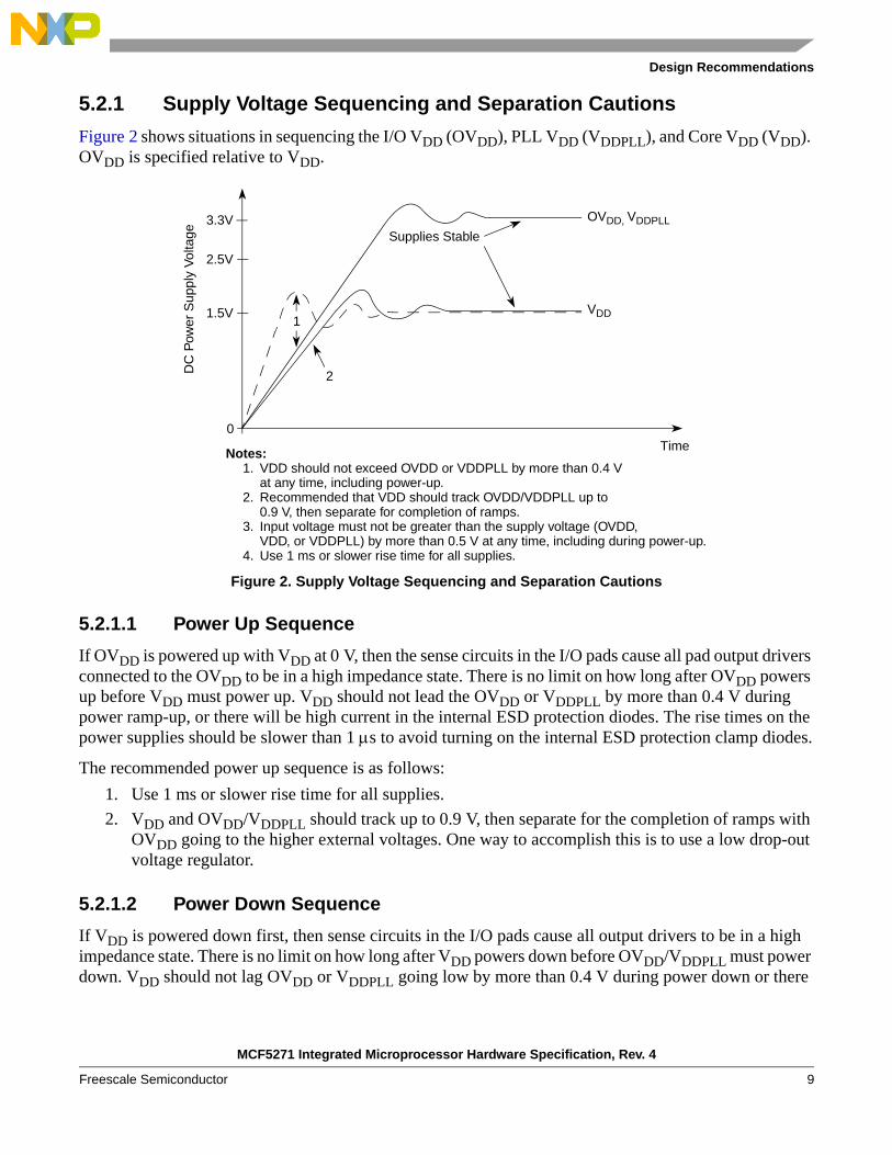
5.2.1 Supply Voltage Sequencing and Separation Cautions
Figure 2 shows situations in sequencing the I/O VDD (OVDD), PLL VDD (VDDPLL), and Core VDD (VDD). OVDD is specified relative to VDD.
Figure 2. Supply Voltage Sequencing and Separation Cautions
5.2.1.1 Power Up Sequence
If OVDD is powered up with VDD at 0 V, then the sense circuits in the I/O pads cause all pad output drivers connected to the OVDD to be in a high impedance state. There is no limit on how long after OVDD powers up before VDD must power up. VDD should not lead the OVDD or VDDPLL by more than 0.4 V during power ramp-up, or there will be high current in the internal ESD protection diodes. The rise times on the power supplies should be slower than 1 μs to avoid turning on the internal ESD protection clamp diodes.
The recommended power up sequence is as follows:1. Use 1 ms or slower rise time for all supplies.2. VDD and OVDD/VDDPLL should track up to 0.9 V, then separate for the completion of ramps with
OVDD going to the higher external voltages. One way to accomplish this is to use a low drop-out voltage regulator.
5.2.1.2 Power Down Sequence
If VDD is powered down first, then sense circuits in the I/O pads cause all output drivers to be in a high impedance state. There is no limit on how long after VDD powers down before OVDD/VDDPLL must power down. VDD should not lag OVDD or VDDPLL going low by more than 0.4 V during power down or there
Supplies Stable
2
1
3.3V
2.5V
1.5V
0TimeNotes:
VDD should not exceed OVDD or VDDPLL by more than 0.4 Vat any time, including power-up.Recommended that VDD should track OVDD/VDDPLL up to0.9 V, then separate for completion of ramps.Input voltage must not be greater than the supply voltage (OVDD,VDD, or VDDPLL) by more than 0.5 V at any time, including during power-up.Use 1 ms or slower rise time for all supplies.
1.
2.
3.
4.
DC
Pow
er S
uppl
y V
olta
ge
VDD
OVDD, VDDPLL
MCF5271 Integrated Microprocessor Hardware Specification, Rev. 4
Freescale Semiconductor 9
Design Recommendations
will be undesired high current in the ESD protection diodes. There are no requirements for the fall times of the power supplies.
The recommended power down sequence is as follows:1. Drop VDD to 0 V.2. Drop OVDD/VDDPLL supplies.
5.3 Decoupling• Place the decoupling caps as close to the pins as possible, but they can be outside the footprint of
the package.• 0.1 μF and 0.01 μF at each supply input
5.4 Buffering• Use bus buffers on all data/address lines for all off-board accesses and for all on-board accesses
when excessive loading is expected. See Section 7, “Electrical Characteristics.”
5.5 Pull-up Recommendations• Use external pull-up resistors on unused inputs. See pin table.
5.6 Clocking Recommendations• Use a multi-layer board with a separate ground plane. • Place the crystal and all other associated components as close to the EXTAL and XTAL (oscillator
pins) as possible. • Do not run a high frequency trace around crystal circuit. • Ensure that the ground for the bypass capacitors is connected to a solid ground trace. • Tie the ground trace to the ground pin nearest EXTAL and XTAL. This prevents large loop currents
in the vicinity of the crystal. • Tie the ground pin to the most solid ground in the system. • Do not connect the trace that connects the oscillator and the ground plane to any other circuit
element. This tends to make the oscillator unstable.• Tie XTAL to ground when an external oscillator is clocking the device.
5.7 Interface Recommendations
5.7.1 SDRAM Controller
5.7.1.1 SDRAM Controller Signals in Synchronous Mode
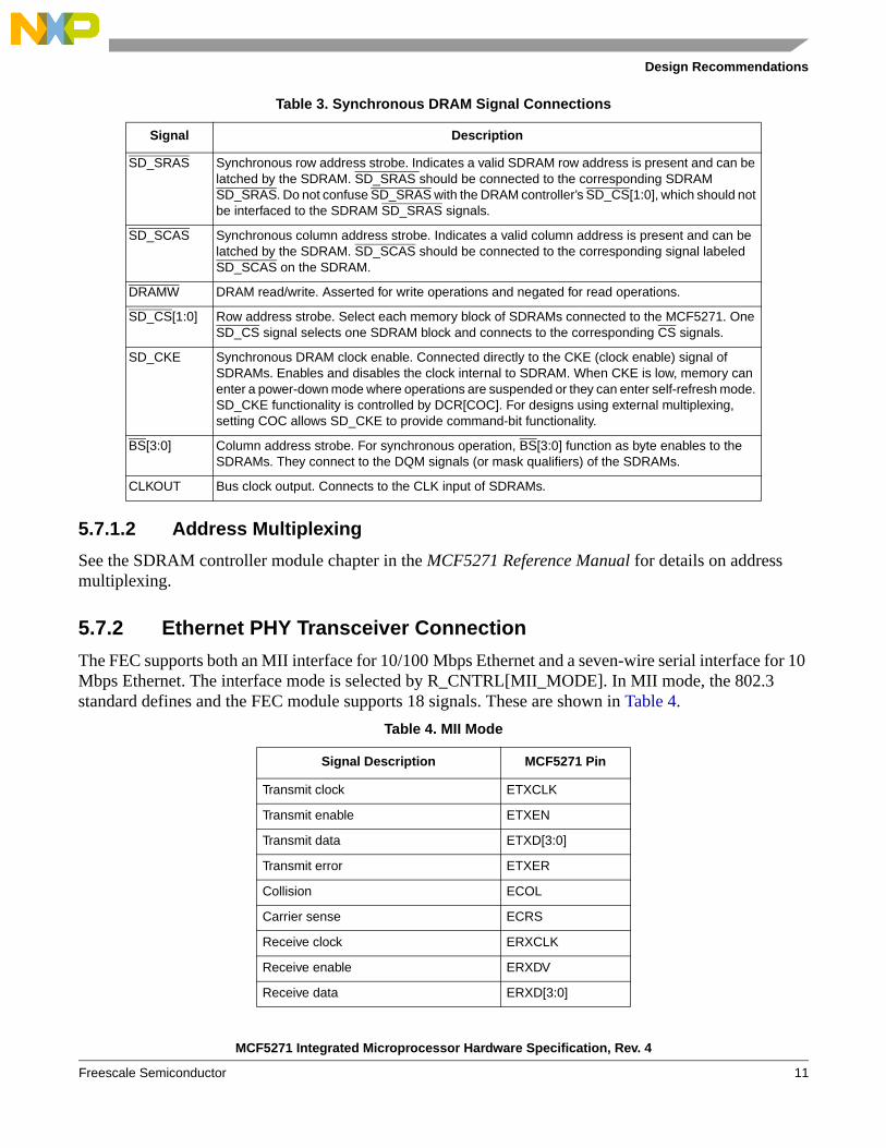
Table 3 shows the behavior of SDRAM signals in synchronous mode.
MCF5271 Integrated Microprocessor Hardware Specification, Rev. 4
Freescale Semiconductor10
Design Recommendations
5.7.1.2 Address Multiplexing
See the SDRAM controller module chapter in the MCF5271 Reference Manual for details on address multiplexing.
5.7.2 Ethernet PHY Transceiver Connection
The FEC supports both an MII interface for 10/100 Mbps Ethernet and a seven-wire serial interface for 10 Mbps Ethernet. The interface mode is selected by R_CNTRL[MII_MODE]. In MII mode, the 802.3 standard defines and the FEC module supports 18 signals. These are shown in Table 4.
Table 3. Synchronous DRAM Signal Connections
Signal Description
SD_SRAS Synchronous row address strobe. Indicates a valid SDRAM row address is present and can be latched by the SDRAM. SD_SRAS should be connected to the corresponding SDRAM SD_SRAS. Do not confuse SD_SRAS with the DRAM controller’s SD_CS[1:0], which should not be interfaced to the SDRAM SD_SRAS signals.
SD_SCAS Synchronous column address strobe. Indicates a valid column address is present and can be latched by the SDRAM. SD_SCAS should be connected to the corresponding signal labeled SD_SCAS on the SDRAM.
DRAMW DRAM read/write. Asserted for write operations and negated for read operations.
SD_CS[1:0] Row address strobe. Select each memory block of SDRAMs connected to the MCF5271. One SD_CS signal selects one SDRAM block and connects to the corresponding CS signals.
SD_CKE Synchronous DRAM clock enable. Connected directly to the CKE (clock enable) signal of SDRAMs. Enables and disables the clock internal to SDRAM. When CKE is low, memory can enter a power-down mode where operations are suspended or they can enter self-refresh mode. SD_CKE functionality is controlled by DCR[COC]. For designs using external multiplexing, setting COC allows SD_CKE to provide command-bit functionality.
BS[3:0] Column address strobe. For synchronous operation, BS[3:0] function as byte enables to the SDRAMs. They connect to the DQM signals (or mask qualifiers) of the SDRAMs.
CLKOUT Bus clock output. Connects to the CLK input of SDRAMs.
Table 4. MII Mode
Signal Description MCF5271 Pin
Transmit clock ETXCLK
Transmit enable ETXEN
Transmit data ETXD[3:0]
Transmit error ETXER
Collision ECOL
Carrier sense ECRS
Receive clock ERXCLK
Receive enable ERXDV
Receive data ERXD[3:0]
MCF5271 Integrated Microprocessor Hardware Specification, Rev. 4
Freescale Semiconductor 11
Mechanicals/Pinouts and Part Numbers
The serial mode interface operates in what is generally referred to as AMD mode. The MCF5271 configuration for seven-wire serial mode connections to the external transceiver are shown in Table 5.
Refer to the M5271EVB evaluation board user’s manual for an example of how to connect an external PHY. Schematics for this board are accessible at the MCF5271 site by navigating to: http://www.freescale.com/coldfire.
5.7.3 BDM
Use the BDM interface as shown in the M5271EVB evaluation board user’s manual. The schematics for this board are accessible at the Freescale website at: http://www.freescale.com/coldfire.
6 Mechanicals/Pinouts and Part NumbersThis section contains drawings showing the pinout and the packaging and mechanical characteristics of the MCF5271 devices. See Table 4 for a list the signal names and pin locations for each device.
Receive error ERXER
Management channel clock EMDC
Management channel serial data EMDIO
Table 5. Seven-Wire Mode Configuration
Signal Description MCF5271 Pin
Transmit clock ETXCLK
Transmit enable ETXEN
Transmit data ETXD[0]
Collision ECOL
Receive clock ERXCLK
Receive enable ERXDV
Receive data ERXD[0]
Unused, configure as PB14 ERXER
Unused input, tie to ground ECRS
Unused, configure as PB[13:11] ERXD[3:1]
Unused output, ignore ETXER
Unused, configure as PB[10:8] ETXD[3:1]
Unused, configure as PB15 EMDC
Input after reset, connect to ground EMDIO
Table 4. MII Mode (continued)
Signal Description MCF5271 Pin
MCF5271 Integrated Microprocessor Hardware Specification, Rev. 4
Freescale Semiconductor12
Mechanicals/Pinouts and Part Numbers
A A
B B
C C
D D
E E
F F
G G
H H
J J
K K
L L
M M
N N
P P
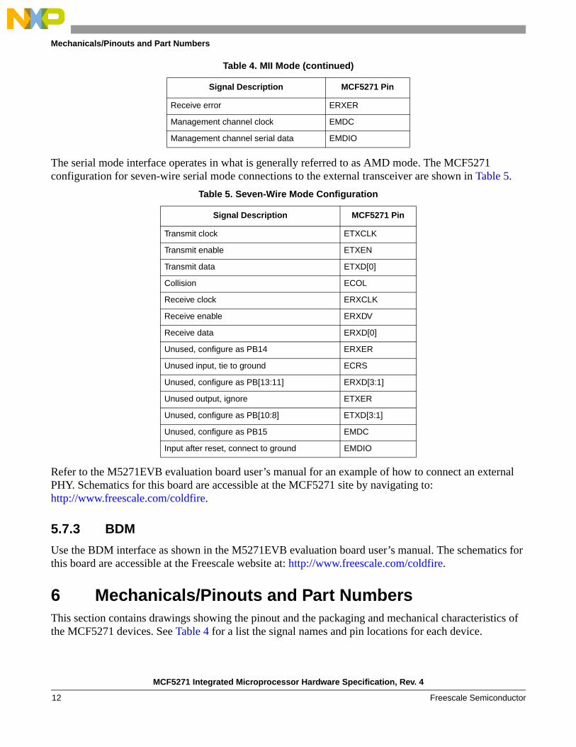
6.1 Pinout—196 MAPBGAThe following figure shows a pinout of the MCF5270/71CVMxxx package.
Figure 3. MCF5270/71CVMxxx Pinout (196 MAPBGA)
1 2 3 4 5 6 7 8 9 10 11 12 13 14
VSS ETXCLK ETXD3 ETXD2 QSPI_DOUT QSPI_CS0 U2RXD U2TXD CS3 CS6 CS4 A20 A17 VSS
ERXD0 ERXER ETXER ETXD0 QSPI_DIN BS3 QSPI_CS1 U1CTS CS7 CS1 A23 A19 A16 A15
ERXD2 ERXD1 ETXEN ETXD1 QSCK BS2 BS0 RTS1 CS2 CS5 A22 A18 A14 A13
ERXCLK ERXDV ERXD3 EMDC EMDIO Core VDD_4 BS1 U1RXD1 U1TXD CS0 A21 A12 A11 A10
ECRS ECOL NC TIN0 VDD VSS VDD SD_CKE VSS VDD A9 A8 A7 A6
U0TXD U0RXD U0CTS DTOUT0 TEST VSS VDD VSS VDD VSS Core VDD_3 A5 A4 A3
D31 D30 U0RTS Core VDD_1
CLK MOD1 VDD VSS VDD VSS NC A2 A1 A0 DTOUT3
D29 D28 D27 D26 CLK MOD0 VSS VDD VDD VDD NC TA TIP TS DTIN3
D25 D24 D23 D22 VSS VDD VSS VDD VSS VDD I2C_SCL I2C_SDA R/W TEA
D21 D20 D19 D18 VDD VDD VSS VDD JTAG_EN RCON SD_ RAS SD_ CAS SD_ WE CLKOUT
D17 D16 D10 Core VDD_2 D3 DTIN1 IRQ5 IRQ1 DTOUT2 PST0 DDATA0 SD_ CS1 SD_ CS0 VSSPLL
D15 D13 D9 D6 D2 DTOUT1 IRQ6 IRQ2 DTIN2 TDI/DSI PST3 DDATA3 VDDPLL EXTAL
D14 D12 D8 D5 D1 OE IRQ7 IRQ3 TRST/DSCLK TDO/DSO PST2 DDATA2 RESET XTAL
VSS D11 D7 D4 D0 TSIZ1 TSIZ0 IRQ4 TCLK/ PSTCLK
TMS/ BKPT PST1 DDATA1 RSTOUT VSS
1 2 3 4 5 6 7 8 9 10 11 12 13 14
MCF5271 Integrated Microprocessor Hardware Specification, Rev. 4
Freescale Semiconductor 13
Mechanicals/Pinouts and Part Numbers
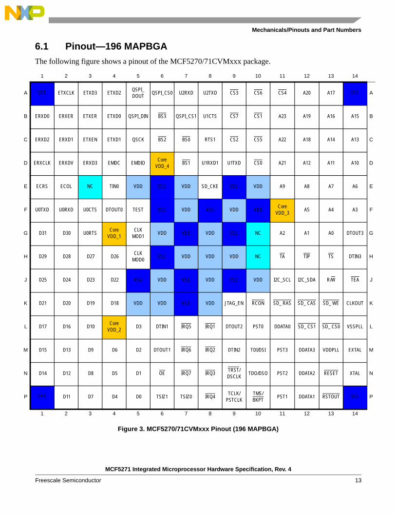
6.2 Package Dimensions—196 MAPBGAFigure 4 shows MCF5270/71CVMxxx package dimensions.
Figure 4. 196 MAPBGA Package Dimensions (Case No. 1128A-01)
X
TOL
Laser mark for pin 1identification inthis area
e13X
D
E
M
S
A1
A2A
0.10 Z
0.20 Z
Z
Rotated 90° ClockwiseDetail K
5
View M-M
e13X
S
M
X0.15 YZ
0.08 Z
3
b196X
Metalized mark for pin 1 identificationin this area14 13 12 11 5 4 3 2
B
C
D
E
F
G
H
J
K
L
4
NOTES:1. Dimensions are in millimeters. 2. Interpret dimensions and tolerances
per ASME Y14.5M, 1994. 3. Dimension b is measured at the
maximum solder ball diameter, parallel to datum plane Z.
4. Datum Z (seating plane) is defined by the spherical crowns of the solder balls.
5. Parallelism measurement shall exclude any effect of mark on top surface of package.
Y
K
M
N
P
A
1610 9
DIMMillimeters
Min Max
A 1.25 1.60
A1 0.27 0.47
A2 1.16 REF
b 0.45 0.55
D 15.00 BSC
E 15.00 BSC
e 1.00 BSC
S 0.50 BSC
196X
MCF5271 Integrated Microprocessor Hardware Specification, Rev. 4
Freescale Semiconductor14
Mechanicals/Pinouts and Part Numbers
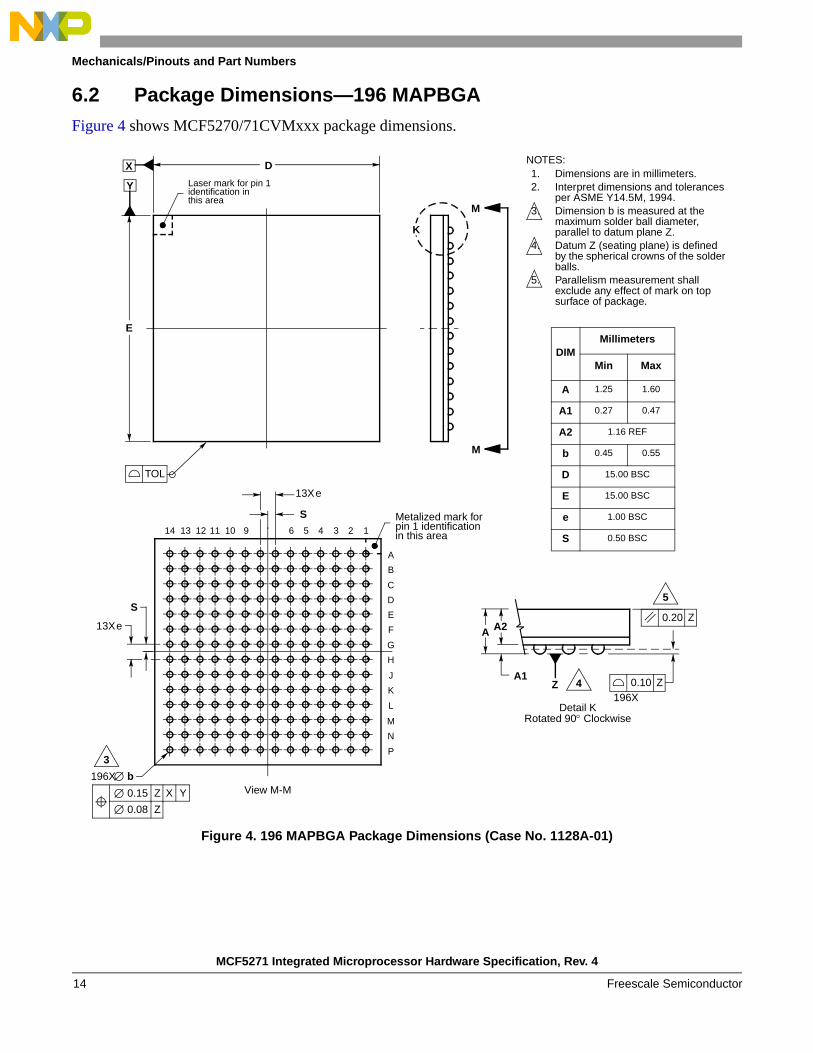
6.3 Pinout—160 QFPFigure 5 shows a pinout of the MCF5271CABxxx package.
Figure 5. MCF5270/71CABxxx Pinout (160 QFP)
160
159
158
157
156
155
154
153
152
151
150
149
148
147
146
145
144
143
142
141
140
139
138
137
136
135
134
133
132
131
130
129
128
127
126
125
124
123
122
121
12011911811711611511411311211111010910810710610510410310210110099989796959493929190898887868584838281
41 42 43 44 45 46 47 48 49 50 51 52 53 54 55 56 57 58 59 60 61 62 63 64 65 66 67 68 69 70 71 72 73 74 75 76 77 78 79 80
12345678910111213141516171819202122232425262728293031323334353637383940
VSS
ERX
ERET
XC
LKET
XEN
ETX
ERET
XD
3ET
XD
2ET
XD
1ET
XD
0EM
DC
EMD
IOQ
SPI_
DO
UT
QSP
I_D
INQ
SPI_
CLK
QSP
I_C
S0O
-VD
DV
SSB
S3B
S2B
S1B
S0Q
SPI_
CS1
/SD
_CK
EO
-VD
DV
SSU
1CTS
U1R
TSU
1RX
DU
1TX
DC
S3C
S2C
S1C
S0O
-VD
DV
SS
A18
A21
A20
A19
A18
A17A16A15A14A13A12O-VDDVSSA11A10A9A8A7A6A5O-VDDVSSCore_Vdd_3A4A3A2A1A0TSTAR/WO-VDDVSSSD_WESD_SCASSD_SRASCLKOUTVSSVDDPLLEXTALXTALVSSPLLRESETRSTOUTO-VDD
A23
O-VDDERXD0ERXD1ERXD2ERXD3ERXDV
ERXCLKECRSECOL
U0TINU0TOUT
U0CTSU0RXDU0TXDU0RTS
Core VDD_1VSS
O-VDDTEST
CLKMOD1CLKMOD0
DATA31DATA30DATA29DATA28DATA27DATA26DATA25DATA24DATA23
VSSO-VDD
DATA22DATA21DATA20DATA19DATA18DATA17DATA16
VSS
O-V
DD
DAT
A15
DAT
A14
DAT
A13
DAT
A12
DAT
A11
DAT
A10
DAT
A9
DAT
A8
DAT
A7
DAT
A6
DAT
A5
Cor
e V
dd_2
VSS
O-V
DD
DAT
A4
DAT
A3
DAT
A2
DAT
A1
DAT
A0
DTI
N1
OE
IRQ
7IR
Q4
IRQ
1D
TIN
2V
SSTC
LK\P
STC
LKO
-VD
DTR
ST/D
SCLK
TMS\
BK
PTTD
O/D
SOTD
I/DSI
PST0
PST1
PST2
PST3
JTA
G_E
NR
CO
NV
SS
MCF5271
MCF5271 Integrated Microprocessor Hardware Specification, Rev. 4
Freescale Semiconductor 15
Mechanicals/Pinouts and Part Numbers
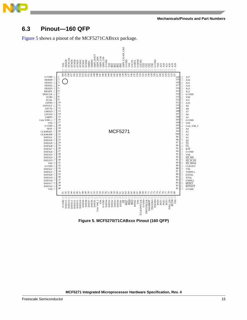
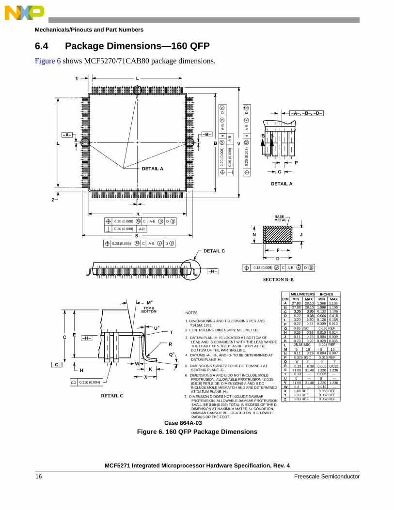
6.4 Package Dimensions—160 QFPFigure 6 shows MCF5270/71CAB80 package dimensions.
Figure 6. 160 QFP Package Dimensions
TOP &BOTTOM
Case 864A-03
D
N
F
J
BASEMETAL
SECTION B–B
DETAIL C
S S
–C–
EC
M×
U×
WK
X
Q×
R
T
H
–H–
B
–A–, –B–, –D–
B
DETAIL A
G
P
S
S
S S
S S A
S
L
Z
LY
DETAIL A
B V
–A– –B–
–H–
DETAIL C
MILLIMETERS INCHESDIM MIN MAX MIN MAXABCDEFGHJKLMNPQR
TUVWXYZ
27.90 28.10 1.098 1.10627.90 28.10 1.098 1.1063.35 3.85 0.132 1.1063.35 3.85
0.009 0.0150.22 0.38
0.009 0.0130.22 0.330.126 0.1383.20 3.50
0.65 BSC 0.026 REF0.010 0.0140.25 0.350.004 0.0090.11 0.230.028 0.0350.70 0.90
25.35 BSC 0.998 REF5° 16° 5° 16°
0.004 0.0070.11 0.190.325 BSC 0.013 REF0° 7° 0° 7°
0.005 0.0120.13 0.30
0.005 —0.13 —0° — 0° —
31.00 31.40 1.220 1.236S
31.00 31.40 1.220 1.2360.016 —0.4 —
1.60 REF 0.063 REF1.33 REF 0.052 REF1.33 REF 0.052 REF
NOTES
1. DIMENSIONING AND TOLERINCING PER ANSIY14.5M, 1982.
2. CONTROLLING DIMENSION: MILLIMETER
3. DATUM PLAN -H- IS LOCATED AT BOTTOM OFLEAD AND IS COINCIDENT WITH THE LEAD WHERETHE LEAD EXITS THE PLASTIC BODY AT THEBOTTOM OF THE PARTING LINE.
4. DATUMS -A-, -B-, AND -D- TO BE DETERMINED ATDATUM PLANE -H-.
5. DIMENSIONS S AND V TO BE DETERMINED ATSEATING PLANE -C-.
6. DIMENSIONS A AND B DO NOT INCLUDE MOLDPROTRUSION. ALLOWABLE PROTRUSION IS 0.25(0.010) PER SIDE. DIMENSIONS A AND B DOINCLUDE MOLD MISMATCH AND ARE DETERMINEDAT DATUM PLANE -H-.
7. DIMENSION D DOES NOT INCLUDE DAMBARPROTRUSION. ALLOWABLE DAMBAR PROTRUSIONSHALL BE 0.08 (0.003) TOTAL IN EXCESS OF THE DDIMENSION AT MAXIMUM MATERIAL CONDITION.DAMBAR CANNOT BE LOCATED ON THE LOWERRADIUS OR THE FOOT.
0.110 (0.004)
A-B DC0.13 (0.005) M
0.20 (0.008) A-B DCM
M0.20 (0.008)
A-B0.20 (0.008)
A-B DC
SS
M M
HA
-BD
HA
-BD
0.20
(0.0
08)
0.20
(0.0
08)
0.20
(0.0
08)
A-B
MCF5271 Integrated Microprocessor Hardware Specification, Rev. 4
Freescale Semiconductor16
Electrical Characteristics
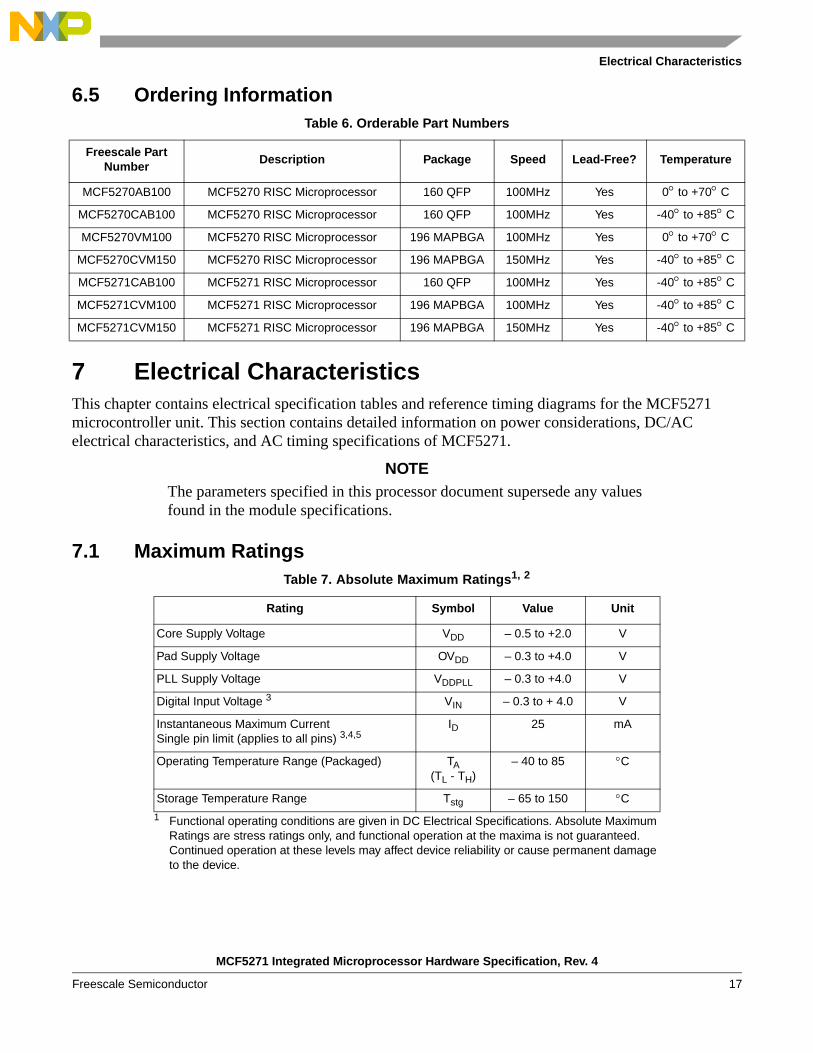
6.5 Ordering Information
7 Electrical CharacteristicsThis chapter contains electrical specification tables and reference timing diagrams for the MCF5271 microcontroller unit. This section contains detailed information on power considerations, DC/AC electrical characteristics, and AC timing specifications of MCF5271.
NOTEThe parameters specified in this processor document supersede any values found in the module specifications.
7.1 Maximum Ratings
Table 6. Orderable Part Numbers
Freescale Part Number
Description Package Speed Lead-Free? Temperature
MCF5270AB100 MCF5270 RISC Microprocessor 160 QFP 100MHz Yes 0° to +70° C
MCF5270CAB100 MCF5270 RISC Microprocessor 160 QFP 100MHz Yes -40° to +85° C
MCF5270VM100 MCF5270 RISC Microprocessor 196 MAPBGA 100MHz Yes 0° to +70° C
MCF5270CVM150 MCF5270 RISC Microprocessor 196 MAPBGA 150MHz Yes -40° to +85° C
MCF5271CAB100 MCF5271 RISC Microprocessor 160 QFP 100MHz Yes -40° to +85° C
MCF5271CVM100 MCF5271 RISC Microprocessor 196 MAPBGA 100MHz Yes -40° to +85° C
MCF5271CVM150 MCF5271 RISC Microprocessor 196 MAPBGA 150MHz Yes -40° to +85° C
Table 7. Absolute Maximum Ratings1, 2
1 Functional operating conditions are given in DC Electrical Specifications. Absolute Maximum Ratings are stress ratings only, and functional operation at the maxima is not guaranteed. Continued operation at these levels may affect device reliability or cause permanent damage to the device.
Rating Symbol Value Unit
Core Supply Voltage VDD – 0.5 to +2.0 V
Pad Supply Voltage OVDD – 0.3 to +4.0 V
PLL Supply Voltage VDDPLL – 0.3 to +4.0 V
Digital Input Voltage 3 VIN – 0.3 to + 4.0 V
Instantaneous Maximum CurrentSingle pin limit (applies to all pins) 3,4,5
ID 25 mA
Operating Temperature Range (Packaged) TA(TL - TH)
– 40 to 85 °C
Storage Temperature Range Tstg – 65 to 150 °C
MCF5271 Integrated Microprocessor Hardware Specification, Rev. 4
Freescale Semiconductor 17
Electrical Characteristics
7.2 Thermal CharacteristicsThe below table lists thermal resistance values.
2 This device contains circuitry protecting against damage due to high static voltage or electrical fields; however, it is advised that normal precautions be taken to avoid application of any voltages higher than maximum-rated voltages to this high-impedance circuit. Reliability of operation is enhanced if unused inputs are tied to an appropriate logic voltage level (e.g., either VSS or OVDD).
3 Input must be current limited to the value specified. To determine the value of the required current-limiting resistor, calculate resistance values for positive and negative clamp voltages, then use the larger of the two values.
4 All functional non-supply pins are internally clamped to VSS and OVDD.5 Power supply must maintain regulation within operating OVDD range during instantaneous
and operating maximum current conditions. If positive injection current (Vin > OVDD) is greater than IDD, the injection current may flow out of OVDD and could result in external power supply going out of regulation. Insure external OVDD load will shunt current greater than maximum injection current. This will be the greatest risk when the processor is not consuming power (ex; no clock).Power supply must maintain regulation within operating OVDD range during instantaneous and operating maximum current conditions.
Table 8. Thermal Characteristics
Characteristic Symbol196
MAPBGA160QFP Unit
Junction to ambient, natural convection Four layer board (2s2p) θJMA 321,2
1 θJMA and Ψjt parameters are simulated in conformance with EIA/JESD Standard 51-2 for natural convection. Motorola recommends the use of θJmA and power dissipation specifications in the system design to prevent device junction temperatures from exceeding the rated specification. System designers should be aware that device junction temperatures can be significantly influenced by board layout and surrounding devices. Conformance to the device junction temperature specification can be verified by physical measurement in the customer’s system using the Ψjt parameter, the device power dissipation, and the method described in EIA/JESD Standard 51-2.
2 Per JEDEC JESD51-6 with the board horizontal.
401,2 °C / W
Junction to ambient (@200 ft/min) Four layer board (2s2p) θJMA 291,2 361,2 °C / W
Junction to board θJB 203
3 Thermal resistance between the die and the printed circuit board in conformance with JEDEC JESD51-8. Board temperature is measured on the top surface of the board near the package.
253 °C / W
Junction to case θJC 104
4 Thermal resistance between the die and the case top surface as measured by the cold plate method (MIL SPEC-883 Method 1012.1).
104 °C / W
Junction to top of package Ψjt 21,5
5 Thermal characterization parameter indicating the temperature difference between package top and the junction temperature per JEDEC JESD51-2. When Greek letters are not available, the thermal characterization parameter is written in conformance with Psi-JT.
21,5 °C / W
Maximum operating junction temperature Tj 104 105 oC
The average chip-junction temperature (TJ) in °C can be obtained from:
(1)
Where:
TJ TA PD ΘJMA×( )+=
MCF5271 Integrated Microprocessor Hardware Specification, Rev. 4
Freescale Semiconductor18
Electrical Characteristics
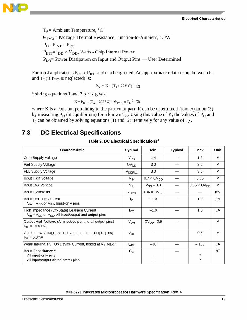
7.3 DC Electrical Specifications
TA= Ambient Temperature, °CΘJMA= Package Thermal Resistance, Junction-to-Ambient, °C/WPD= PINT + PI/OPINT= IDD × VDD, Watts - Chip Internal PowerPI/O= Power Dissipation on Input and Output Pins — User Determined
For most applications PI/O < PINT and can be ignored. An approximate relationship between PD and TJ (if PI/O is neglected) is:
(2)
Solving equations 1 and 2 for K gives:K = PD × (TA + 273 °C) + ΘJMA × PD
2 (3)
where K is a constant pertaining to the particular part. K can be determined from equation (3) by measuring PD (at equilibrium) for a known TA. Using this value of K, the values of PD and TJ can be obtained by solving equations (1) and (2) iteratively for any value of TA.
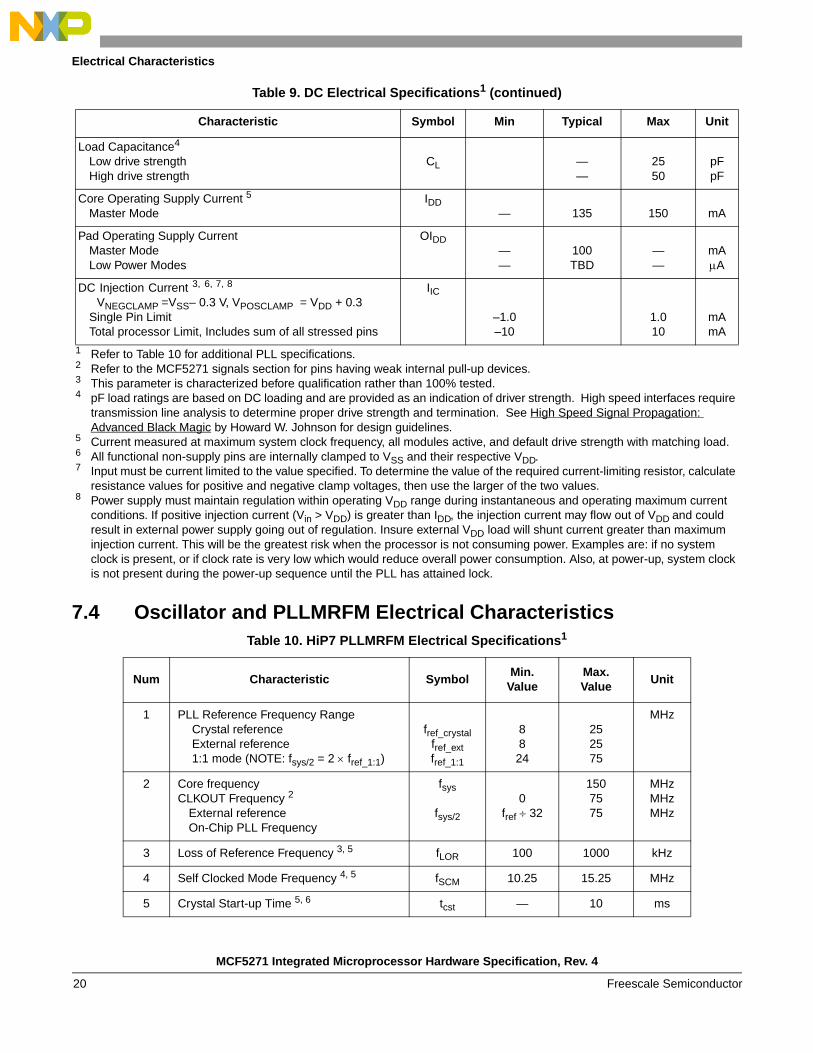
Table 9. DC Electrical Specifications1
Characteristic Symbol Min Typical Max Unit
Core Supply Voltage VDD 1.4 — 1.6 V
Pad Supply Voltage OVDD 3.0 — 3.6 V
PLL Supply Voltage VDDPLL 3.0 — 3.6 V
Input High Voltage VIH 0.7 × OVDD — 3.65 V
Input Low Voltage VIL VSS – 0.3 — 0.35 × OVDD V
Input Hysteresis VHYS 0.06 × OVDD — — mV
Input Leakage CurrentVin = VDD or VSS, Input-only pins
Iin –1.0 — 1.0 μA
High Impedance (Off-State) Leakage CurrentVin = VDD or VSS, All input/output and output pins
IOZ –1.0 — 1.0 μA
Output High Voltage (All input/output and all output pins)IOH = –5.0 mA
VOH OVDD - 0.5 — — V
Output Low Voltage (All input/output and all output pins)IOL = 5.0mA
VOL — — 0.5 V
Weak Internal Pull Up Device Current, tested at VIL Max.2 IAPU –10 — – 130 μA
Input Capacitance 3
All input-only pinsAll input/output (three-state) pins
Cin——
—77
pF
PD K TJ 273°C+( )÷=
MCF5271 Integrated Microprocessor Hardware Specification, Rev. 4
Freescale Semiconductor 19
Electrical Characteristics
7.4 Oscillator and PLLMRFM Electrical Characteristics
Load Capacitance4
Low drive strengthHigh drive strength
CL ——
2550
pFpF
Core Operating Supply Current 5
Master ModeIDD
— 135 150 mA
Pad Operating Supply CurrentMaster ModeLow Power Modes
OIDD——
100TBD
——
mAμA
DC Injection Current 3, 6, 7, 8
VNEGCLAMP =VSS– 0.3 V, VPOSCLAMP = VDD + 0.3Single Pin LimitTotal processor Limit, Includes sum of all stressed pins
IIC
–1.0–10
1.010
mAmA
1 Refer to Table 10 for additional PLL specifications.2 Refer to the MCF5271 signals section for pins having weak internal pull-up devices.3 This parameter is characterized before qualification rather than 100% tested.4 pF load ratings are based on DC loading and are provided as an indication of driver strength. High speed interfaces require
transmission line analysis to determine proper drive strength and termination. See High Speed Signal Propagation: Advanced Black Magic by Howard W. Johnson for design guidelines.
5 Current measured at maximum system clock frequency, all modules active, and default drive strength with matching load.6 All functional non-supply pins are internally clamped to VSS and their respective VDD.7 Input must be current limited to the value specified. To determine the value of the required current-limiting resistor, calculate
resistance values for positive and negative clamp voltages, then use the larger of the two values.8 Power supply must maintain regulation within operating VDD range during instantaneous and operating maximum current
conditions. If positive injection current (Vin > VDD) is greater than IDD, the injection current may flow out of VDD and could result in external power supply going out of regulation. Insure external VDD load will shunt current greater than maximum injection current. This will be the greatest risk when the processor is not consuming power. Examples are: if no system clock is present, or if clock rate is very low which would reduce overall power consumption. Also, at power-up, system clock is not present during the power-up sequence until the PLL has attained lock.
Table 10. HiP7 PLLMRFM Electrical Specifications1
Num Characteristic SymbolMin.
ValueMax.Value
Unit
1 PLL Reference Frequency Range Crystal reference External reference 1:1 mode (NOTE: fsys/2 = 2 × fref_1:1)
fref_crystal fref_ext fref_1:1
8824
252575
MHz
2 Core frequency CLKOUT Frequency 2
External referenceOn-Chip PLL Frequency
fsys
fsys/2 0
fref ÷ 32
1507575
MHzMHzMHz
3 Loss of Reference Frequency 3, 5 fLOR 100 1000 kHz
4 Self Clocked Mode Frequency 4, 5 fSCM 10.25 15.25 MHz
5 Crystal Start-up Time 5, 6 tcst — 10 ms
Table 9. DC Electrical Specifications1 (continued)
Characteristic Symbol Min Typical Max Unit
MCF5271 Integrated Microprocessor Hardware Specification, Rev. 4
Freescale Semiconductor20
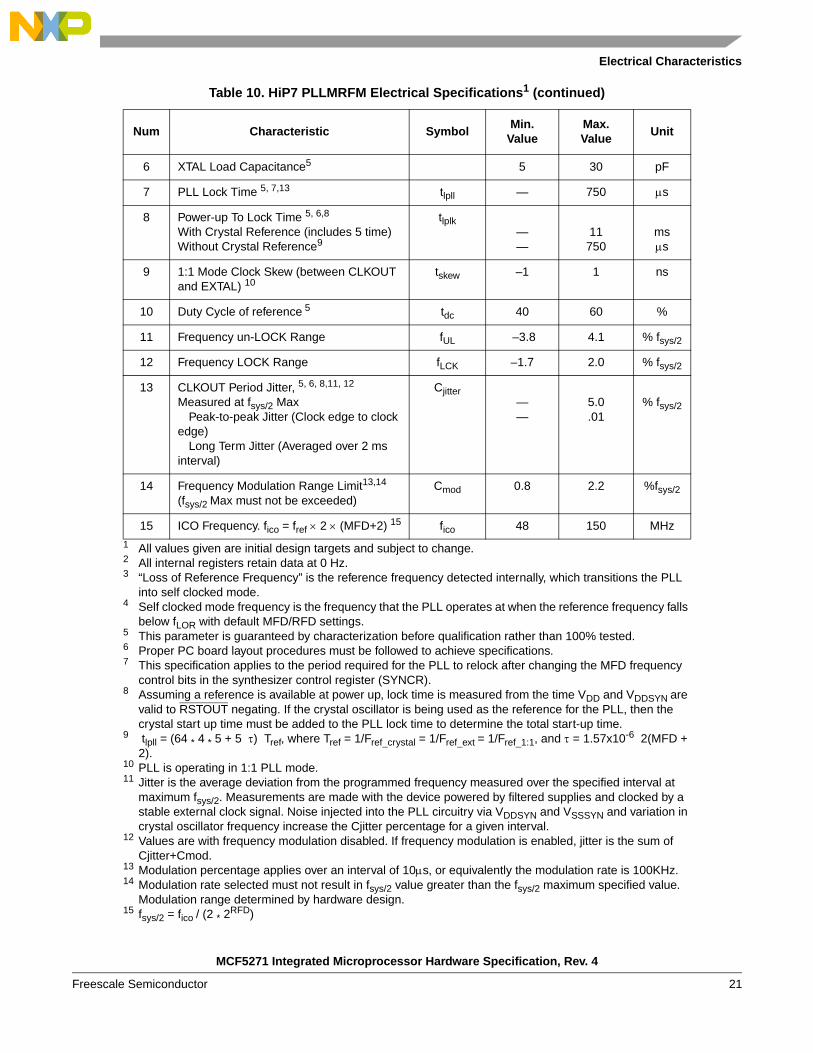
Electrical Characteristics
6 XTAL Load Capacitance5 5 30 pF
7 PLL Lock Time 5, 7,13 tlpll — 750 μs
8 Power-up To Lock Time 5, 6,8
With Crystal Reference (includes 5 time)Without Crystal Reference9
tlplk ——
11750
msμs
9 1:1 Mode Clock Skew (between CLKOUT and EXTAL) 10
tskew –1 1 ns
10 Duty Cycle of reference 5 tdc 40 60 %
11 Frequency un-LOCK Range fUL –3.8 4.1 % fsys/2
12 Frequency LOCK Range fLCK –1.7 2.0 % fsys/2
13 CLKOUT Period Jitter, 5, 6, 8,11, 12
Measured at fsys/2 MaxPeak-to-peak Jitter (Clock edge to clock
edge)Long Term Jitter (Averaged over 2 ms
interval)
Cjitter ——
5.0.01
% fsys/2
14 Frequency Modulation Range Limit13,14
(fsys/2 Max must not be exceeded)Cmod 0.8 2.2 %fsys/2
15 ICO Frequency. fico = fref × 2 × (MFD+2) 15 fico 48 150 MHz
1 All values given are initial design targets and subject to change.2 All internal registers retain data at 0 Hz.3 “Loss of Reference Frequency” is the reference frequency detected internally, which transitions the PLL
into self clocked mode.4 Self clocked mode frequency is the frequency that the PLL operates at when the reference frequency falls
below fLOR with default MFD/RFD settings.5 This parameter is guaranteed by characterization before qualification rather than 100% tested.6 Proper PC board layout procedures must be followed to achieve specifications.7 This specification applies to the period required for the PLL to relock after changing the MFD frequency
control bits in the synthesizer control register (SYNCR).8 Assuming a reference is available at power up, lock time is measured from the time VDD and VDDSYN are
valid to RSTOUT negating. If the crystal oscillator is being used as the reference for the PLL, then the crystal start up time must be added to the PLL lock time to determine the total start-up time.
9 tlpll = (64 * 4 * 5 + 5 τ) Tref, where Tref = 1/Fref_crystal = 1/Fref_ext = 1/Fref_1:1, and τ = 1.57x10⁻⁶ 2(MFD + 2).
10 PLL is operating in 1:1 PLL mode.11 Jitter is the average deviation from the programmed frequency measured over the specified interval at
maximum fsys/2. Measurements are made with the device powered by filtered supplies and clocked by a stable external clock signal. Noise injected into the PLL circuitry via VDDSYN and VSSSYN and variation in crystal oscillator frequency increase the Cjitter percentage for a given interval.
12 Values are with frequency modulation disabled. If frequency modulation is enabled, jitter is the sum of Cjitter+Cmod.
13 Modulation percentage applies over an interval of 10μs, or equivalently the modulation rate is 100KHz.14 Modulation rate selected must not result in fsys/2 value greater than the fsys/2 maximum specified value.
Modulation range determined by hardware design.15 fsys/2 = fico / (2 * 2
RFD)
Table 10. HiP7 PLLMRFM Electrical Specifications1 (continued)
Num Characteristic SymbolMin.
ValueMax.Value
Unit
MCF5271 Integrated Microprocessor Hardware Specification, Rev. 4
Freescale Semiconductor 21
Electrical Characteristics
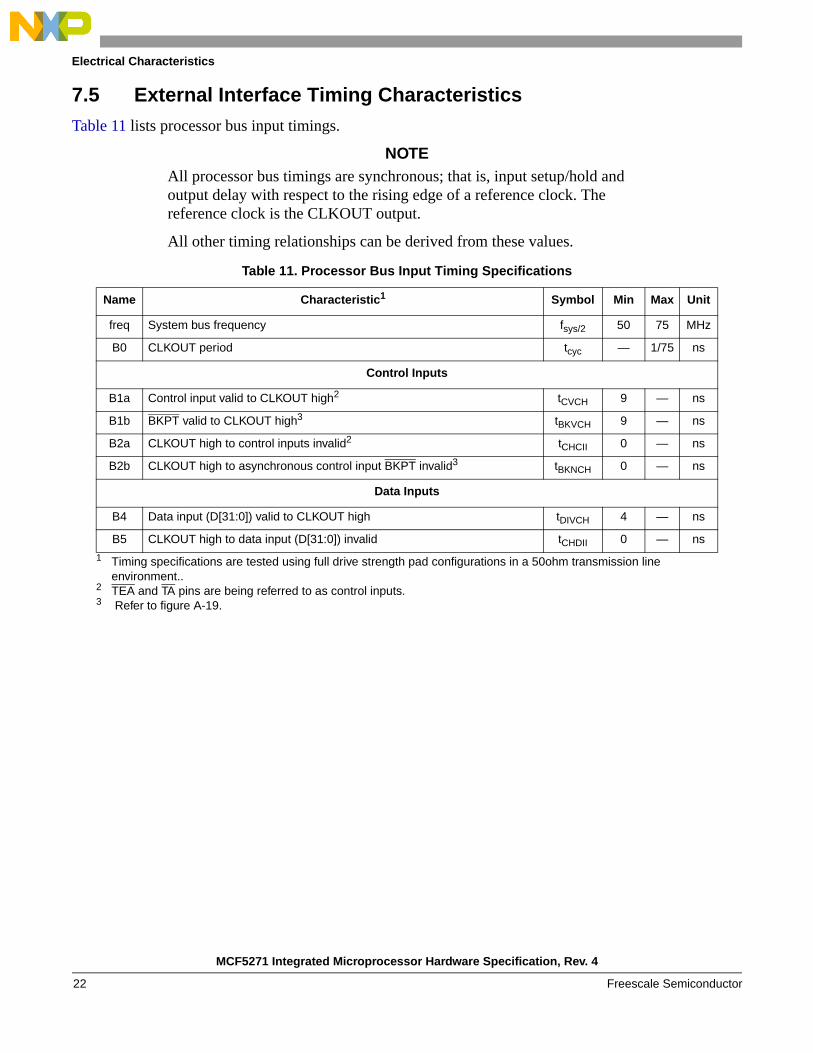
7.5 External Interface Timing CharacteristicsTable 11 lists processor bus input timings.
NOTEAll processor bus timings are synchronous; that is, input setup/hold and output delay with respect to the rising edge of a reference clock. The reference clock is the CLKOUT output.
All other timing relationships can be derived from these values.
Table 11. Processor Bus Input Timing Specifications
Name Characteristic1
1 Timing specifications are tested using full drive strength pad configurations in a 50ohm transmission line environment..
Symbol Min Max Unit
freq System bus frequency fsys/2 50 75 MHz
B0 CLKOUT period tcyc — 1/75 ns
Control Inputs
B1a Control input valid to CLKOUT high2
2 TEA and TA pins are being referred to as control inputs.
tCVCH 9 — ns
B1b BKPT valid to CLKOUT high3
3 Refer to figure A-19.
tBKVCH 9 — ns
B2a CLKOUT high to control inputs invalid2 tCHCII 0 — ns
B2b CLKOUT high to asynchronous control input BKPT invalid3 tBKNCH 0 — ns
Data Inputs
B4 Data input (D[31:0]) valid to CLKOUT high tDIVCH 4 — ns
B5 CLKOUT high to data input (D[31:0]) invalid tCHDII 0 — ns
MCF5271 Integrated Microprocessor Hardware Specification, Rev. 4
Freescale Semiconductor22
Electrical Characteristics
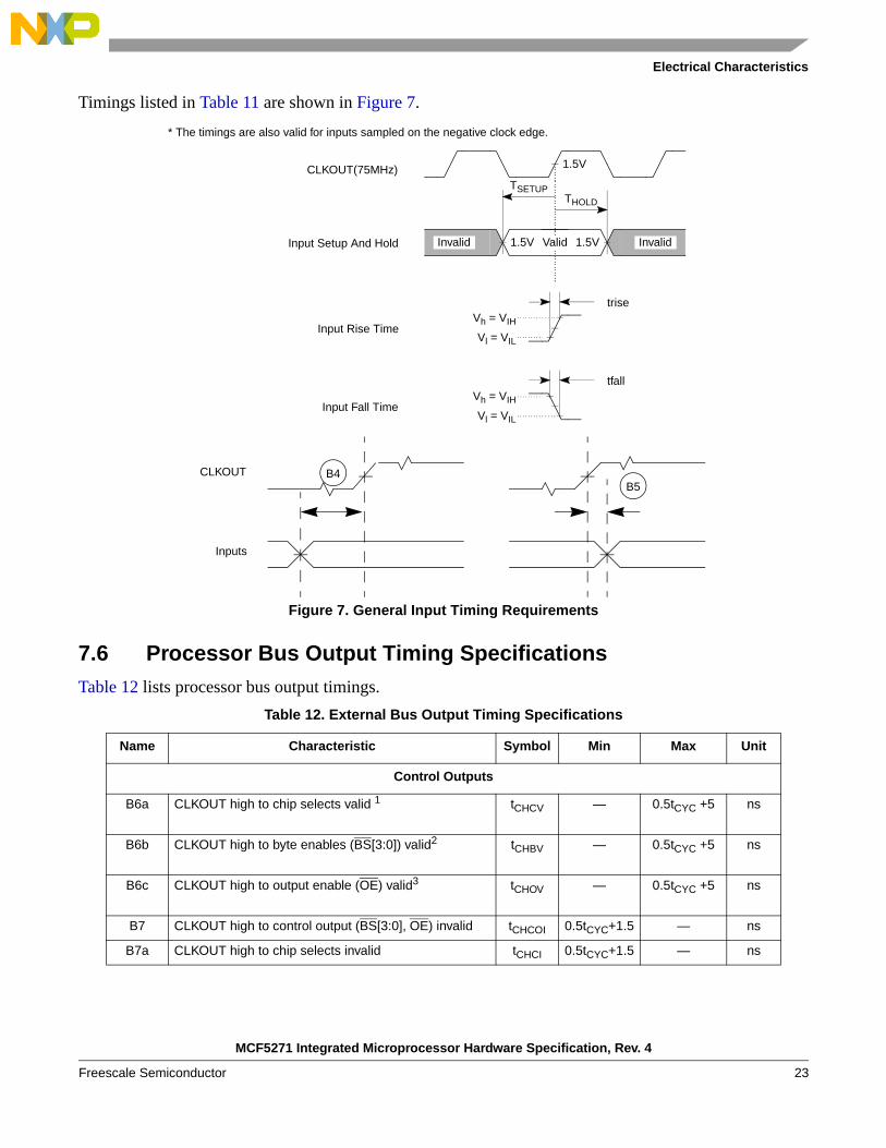
Timings listed in Table 11 are shown in Figure 7.
Figure 7. General Input Timing Requirements
7.6 Processor Bus Output Timing SpecificationsTable 12 lists processor bus output timings.
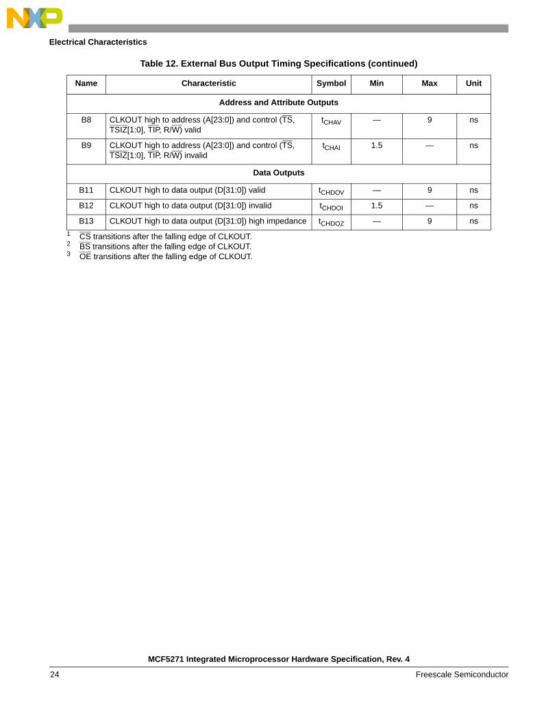
Table 12. External Bus Output Timing Specifications
Name Characteristic Symbol Min Max Unit
Control Outputs
B6a CLKOUT high to chip selects valid 1 tCHCV — 0.5tCYC +5 ns
B6b CLKOUT high to byte enables (BS[3:0]) valid2 tCHBV — 0.5tCYC +5 ns
B6c CLKOUT high to output enable (OE) valid3 tCHOV — 0.5tCYC +5 ns
B7 CLKOUT high to control output (BS[3:0], OE) invalid tCHCOI 0.5tCYC+1.5 — ns
B7a CLKOUT high to chip selects invalid tCHCI 0.5tCYC+1.5 — ns
Invalid Invalid
CLKOUT(75MHz)TSETUP
THOLD
Input Setup And Hold
1.5V
trise Vh = VIH
Vl = VIL
1.5V1.5V Valid
tfallVh = VIH
Vl = VIL
Input Rise Time
Input Fall Time
* The timings are also valid for inputs sampled on the negative clock edge.
Inputs
CLKOUT B4B5
MCF5271 Integrated Microprocessor Hardware Specification, Rev. 4
Freescale Semiconductor 23
Electrical Characteristics
Address and Attribute Outputs
B8 CLKOUT high to address (A[23:0]) and control (TS, TSIZ[1:0], TIP, R/W) valid
tCHAV — 9 ns
B9 CLKOUT high to address (A[23:0]) and control (TS, TSIZ[1:0], TIP, R/W) invalid
tCHAI 1.5 — ns
Data Outputs
B11 CLKOUT high to data output (D[31:0]) valid tCHDOV — 9 ns
B12 CLKOUT high to data output (D[31:0]) invalid tCHDOI 1.5 — ns
B13 CLKOUT high to data output (D[31:0]) high impedance tCHDOZ — 9 ns
1 CS transitions after the falling edge of CLKOUT.2 BS transitions after the falling edge of CLKOUT.3 OE transitions after the falling edge of CLKOUT.
Table 12. External Bus Output Timing Specifications (continued)
Name Characteristic Symbol Min Max Unit
MCF5271 Integrated Microprocessor Hardware Specification, Rev. 4
Freescale Semiconductor24
Electrical Characteristics
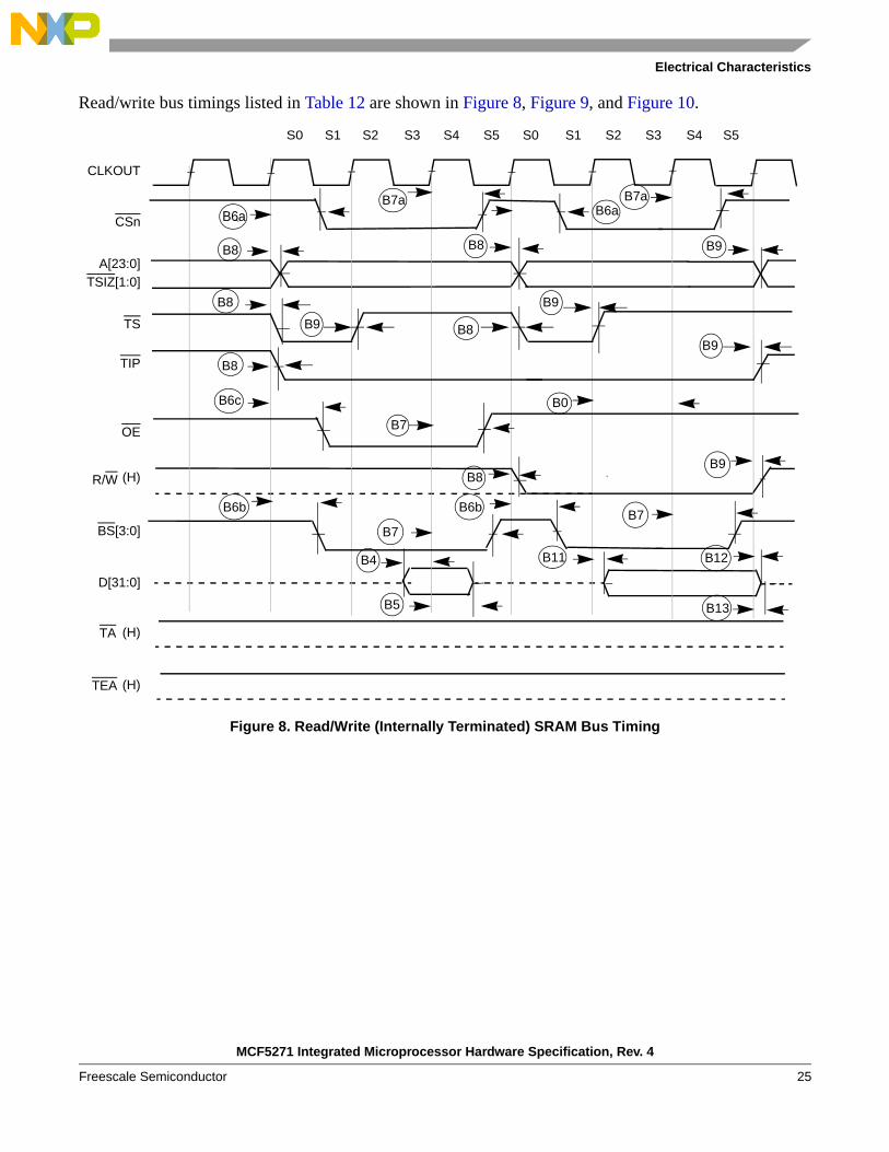
Read/write bus timings listed in Table 12 are shown in Figure 8, Figure 9, and Figure 10.
Figure 8. Read/Write (Internally Terminated) SRAM Bus Timing
B12
B13
B8
CLKOUT
CSn
A[23:0]
R/W
BS[3:0]
D[31:0]
TA
(H)
(H)
S0 S2 S3S1 S4 S5 S0 S1 S2 S3 S4 S5
TEA (H)
B6a
B8
B7a
B6c
B7
B6b
B7
B4
B5
B11
B9
B9
B6b
OE
B0
B7
B9TS
TIP
B8
B8B9
B8
B9TSIZ[1:0]
B7aB6a
B8
MCF5271 Integrated Microprocessor Hardware Specification, Rev. 4
Freescale Semiconductor 25
Electrical Characteristics
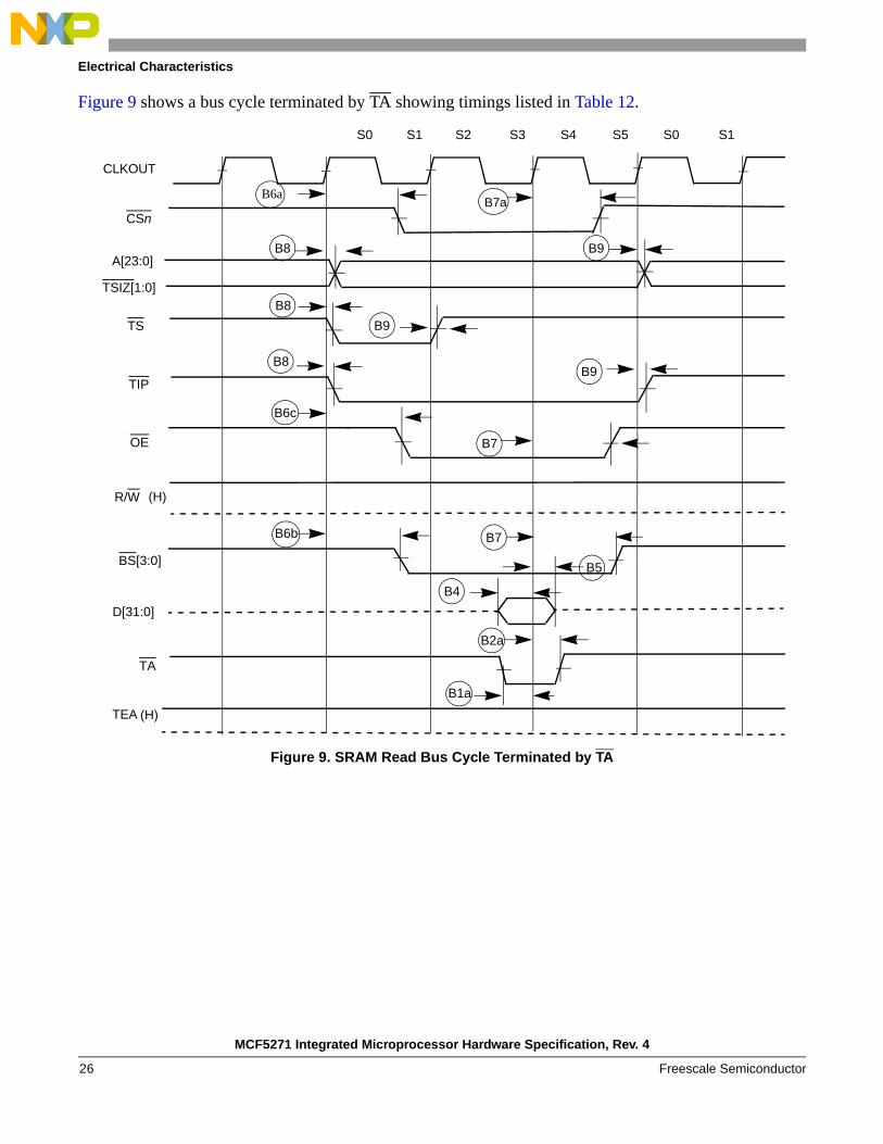
Figure 9 shows a bus cycle terminated by TA showing timings listed in Table 12.
Figure 9. SRAM Read Bus Cycle Terminated by TA
B8
B9
B6a
CLKOUT
CSn
A[23:0]
OE
R/W
BS[3:0]
TA
(H)
S0 S2 S3S1 S4 S5 S0 S1
TEA (H)
B8
B7a
B9
B6c
B7
B6b B7
B2a
B1a
D[31:0]B4
B5
B8TS
B9TIP
TSIZ[1:0]
MCF5271 Integrated Microprocessor Hardware Specification, Rev. 4
Freescale Semiconductor26
Electrical Characteristics
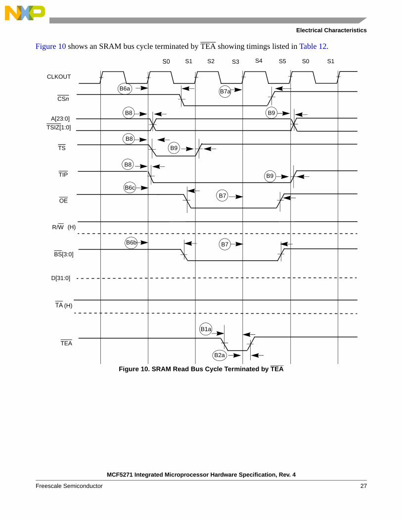
Figure 10 shows an SRAM bus cycle terminated by TEA showing timings listed in Table 12.
Figure 10. SRAM Read Bus Cycle Terminated by TEA
CLKOUT
CSn
A[23:0]
OE
R/W
BS[3:0]
TEA
(H)
S0 S2 S3S1 S4 S5 S0 S1
TA (H)
B6a
B8
B7a
B9
B6cB7
B6b B7
B2a
B1a
D[31:0]
B8B9TS
B9TIP
B8
TSIZ[1:0]
MCF5271 Integrated Microprocessor Hardware Specification, Rev. 4
Freescale Semiconductor 27
Electrical Characteristics
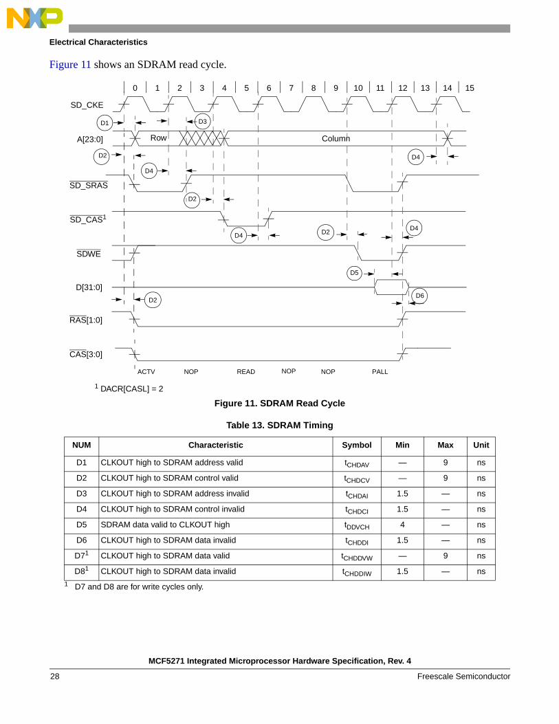
Figure 11 shows an SDRAM read cycle.
Figure 11. SDRAM Read Cycle
Table 13. SDRAM Timing
NUM Characteristic Symbol Min Max Unit
D1 CLKOUT high to SDRAM address valid tCHDAV — 9 ns
D2 CLKOUT high to SDRAM control valid tCHDCV — 9 ns
D3 CLKOUT high to SDRAM address invalid tCHDAI 1.5 — ns
D4 CLKOUT high to SDRAM control invalid tCHDCI 1.5 — ns
D5 SDRAM data valid to CLKOUT high tDDVCH 4 — ns
D6 CLKOUT high to SDRAM data invalid tCHDDI 1.5 — ns
D71
1 D7 and D8 are for write cycles only.
CLKOUT high to SDRAM data valid tCHDDVW — 9 ns
D81 CLKOUT high to SDRAM data invalid tCHDDIW 1.5 — ns
A[23:0]
SD_SRAS
D[31:0]
ACTV NOP PALLNOP
RAS[1:0]
READ
Column
SD_CKE
0
SDWE
CAS[3:0]
1 2 3 4 5 6 7 8 9 10 11 12 13 14 15
D1
D2
D4
D6
D5
D4
1 DACR[CASL] = 2
SD_CAS1
NOP
D4
Row
D3
D2
D2
D2
D4
MCF5271 Integrated Microprocessor Hardware Specification, Rev. 4
Freescale Semiconductor28
Electrical Characteristics
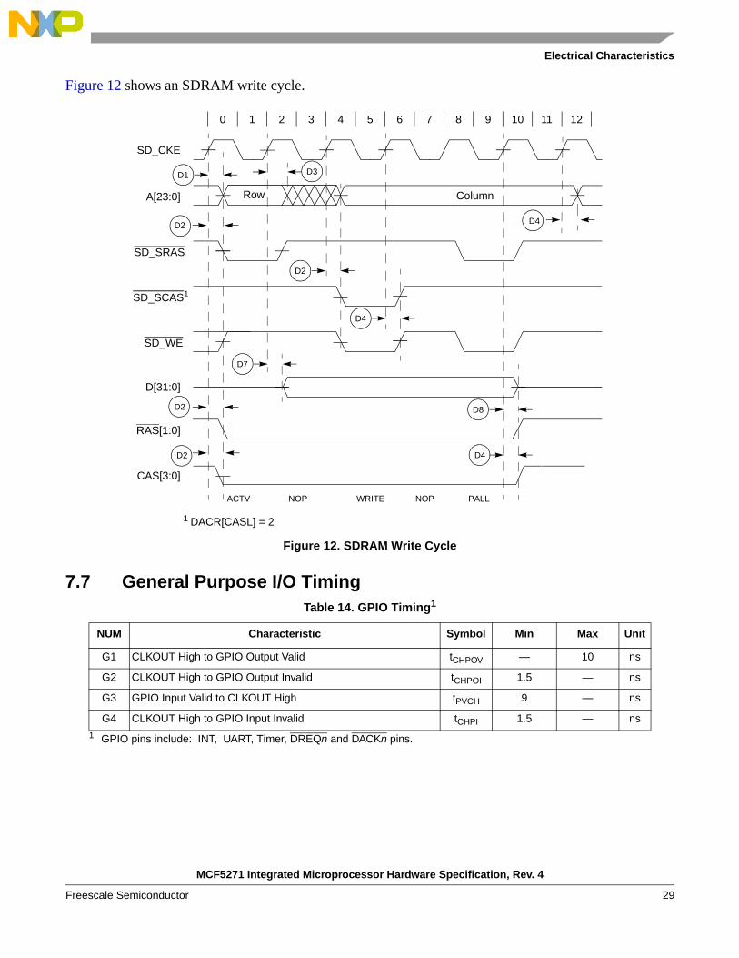
Figure 12 shows an SDRAM write cycle.
Figure 12. SDRAM Write Cycle
7.7 General Purpose I/O TimingTable 14. GPIO Timing1
1 GPIO pins include: INT, UART, Timer, DREQn and DACKn pins.
NUM Characteristic Symbol Min Max Unit
G1 CLKOUT High to GPIO Output Valid tCHPOV — 10 ns
G2 CLKOUT High to GPIO Output Invalid tCHPOI 1.5 — ns
G3 GPIO Input Valid to CLKOUT High tPVCH 9 — ns
G4 CLKOUT High to GPIO Input Invalid tCHPI 1.5 — ns
A[23:0]
SD_SRAS
SD_SCAS1
D[31:0]
ACTV PALLNOP
RAS[1:0]
WRITE
Row Column
SD_CKE
SD_WE
CAS[3:0]
D1
D2
D4
D8
0 1 2 3 4 5 6 7 8 9 10 11 12
D7
NOP
1 DACR[CASL] = 2
D4
D3
D2
D2
D4D2
MCF5271 Integrated Microprocessor Hardware Specification, Rev. 4
Freescale Semiconductor 29
Electrical Characteristics
Figure 13. GPIO Timing
7.8 Reset and Configuration Override Timing
Figure 14. RESET and Configuration Override Timing
Refer to the chip configuration module (CCM) chapter in the device’s reference manual for more information.
Table 15. Reset and Configuration Override Timing(VDD = 2.7 to 3.6 V, VSS = 0 V, TA = TL to TH)1
1 All AC timing is shown with respect to 50% VDD levels unless otherwise noted.
NUM Characteristic Symbol Min Max Unit
R1 RESET Input valid to CLKOUT High tRVCH 9 — ns
R2 CLKOUT High to RESET Input invalid tCHRI 1.5 — ns
R3 RESET Input valid Time 2
2 During low power STOP, the synchronizers for the RESET input are bypassed and RESET is asserted asynchronously to the system. Thus, RESET must be held a minimum of 100 ns.
tRIVT 5 — tCYC
R4 CLKOUT High to RSTOUT Valid tCHROV — 10 ns
R5 RSTOUT valid to Config. Overrides valid tROVCV 0 — ns
R6 Configuration Override Setup Time to RSTOUT invalid tCOS 20 — tCYC
R7 Configuration Override Hold Time after RSTOUT invalid tCOH 0 — ns
R8 RSTOUT invalid to Configuration Override High Impedance tROICZ — 1 tCYC
G2G1
G4G3
CLKOUT
GPIO Outputs
GPIO Inputs
R1 R2
CLKOUT
RESET
RSTOUT
R3
R4
R8R7R6R5
Configuration Overrides*:
R4
(RCON, Override pins])
MCF5271 Integrated Microprocessor Hardware Specification, Rev. 4
Freescale Semiconductor30
Electrical Characteristics
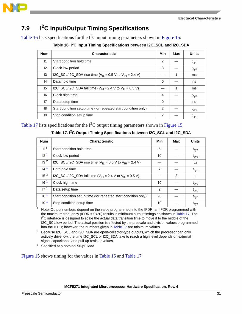
7.9 I2C Input/Output Timing SpecificationsTable 16 lists specifications for the I2C input timing parameters shown in Figure 15.
Table 17 lists specifications for the I2C output timing parameters shown in Figure 15.
Figure 15 shows timing for the values in Table 16 and Table 17.
Table 16. I2C Input Timing Specifications between I2C_SCL and I2C_SDA
Num Characteristic Min Max Units
I1 Start condition hold time 2 — tcyc
I2 Clock low period 8 — tcyc
I3 I2C_SCL/I2C_SDA rise time (VIL = 0.5 V to VIH = 2.4 V) — 1 ms
I4 Data hold time 0 — ns
I5 I2C_SCL/I2C_SDA fall time (VIH = 2.4 V to VIL = 0.5 V) — 1 ms
I6 Clock high time 4 — tcyc
I7 Data setup time 0 — ns
I8 Start condition setup time (for repeated start condition only) 2 — tcyc
I9 Stop condition setup time 2 — tcyc
Table 17. I2C Output Timing Specifications between I2C_SCL and I2C_SDA
Num Characteristic Min Max Units
I11
1 Note: Output numbers depend on the value programmed into the IFDR; an IFDR programmed with the maximum frequency (IFDR = 0x20) results in minimum output timings as shown in Table 17. The I2C interface is designed to scale the actual data transition time to move it to the middle of the I2C_SCL low period. The actual position is affected by the prescale and division values programmed into the IFDR; however, the numbers given in Table 17 are minimum values.
Start condition hold time 6 — tcyc
I2 1 Clock low period 10 — tcyc
I3 2
2 Because I2C_SCL and I2C_SDA are open-collector-type outputs, which the processor can only actively drive low, the time I2C_SCL or I2C_SDA take to reach a high level depends on external signal capacitance and pull-up resistor values.
I2C_SCL/I2C_SDA rise time (VIL = 0.5 V to VIH = 2.4 V) — — µs
I4 1 Data hold time 7 — tcyc
I5 3
3 Specified at a nominal 50-pF load.
I2C_SCL/I2C_SDA fall time (VIH = 2.4 V to VIL = 0.5 V) — 3 ns
I6 1 Clock high time 10 — tcyc
I7 1 Data setup time 2 — tcyc
I8 1 Start condition setup time (for repeated start condition only) 20 — tcyc
I9 1 Stop condition setup time 10 — tcyc
MCF5271 Integrated Microprocessor Hardware Specification, Rev. 4
Freescale Semiconductor 31
Electrical Characteristics
Figure 15. I2C Input/Output Timings
7.10 Fast Ethernet AC Timing SpecificationsMII signals use TTL signal levels compatible with devices operating at either 5.0 V or 3.3 V.
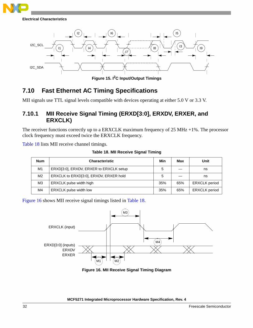
7.10.1 MII Receive Signal Timing (ERXD[3:0], ERXDV, ERXER, and ERXCLK)
The receiver functions correctly up to a ERXCLK maximum frequency of 25 MHz +1%. The processor clock frequency must exceed twice the ERXCLK frequency.
Table 18 lists MII receive channel timings.
Figure 16 shows MII receive signal timings listed in Table 18.
Figure 16. MII Receive Signal Timing Diagram
Table 18. MII Receive Signal Timing
Num Characteristic Min Max Unit
M1 ERXD[3:0], ERXDV, ERXER to ERXCLK setup 5 — ns
M2 ERXCLK to ERXD[3:0], ERXDV, ERXER hold 5 — ns
M3 ERXCLK pulse width high 35% 65% ERXCLK period
M4 ERXCLK pulse width low 35% 65% ERXCLK period
I2 I6
I1 I4I7
I8 I9
I5
I3I2C_SCL
I2C_SDA
M1 M2
ERXCLK (input)
ERXD[3:0] (inputs)ERXDVERXER
M3
M4
MCF5271 Integrated Microprocessor Hardware Specification, Rev. 4
Freescale Semiconductor32
Electrical Characteristics
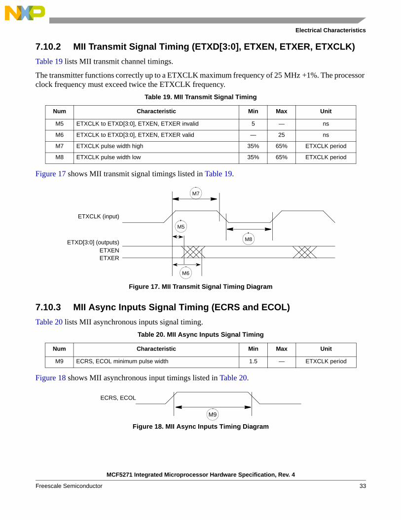
7.10.2 MII Transmit Signal Timing (ETXD[3:0], ETXEN, ETXER, ETXCLK)
Table 19 lists MII transmit channel timings.
The transmitter functions correctly up to a ETXCLK maximum frequency of 25 MHz +1%. The processor clock frequency must exceed twice the ETXCLK frequency.
Figure 17 shows MII transmit signal timings listed in Table 19.
Figure 17. MII Transmit Signal Timing Diagram
7.10.3 MII Async Inputs Signal Timing (ECRS and ECOL)
Table 20 lists MII asynchronous inputs signal timing.
Figure 18 shows MII asynchronous input timings listed in Table 20.
Figure 18. MII Async Inputs Timing Diagram
Table 19. MII Transmit Signal Timing
Num Characteristic Min Max Unit
M5 ETXCLK to ETXD[3:0], ETXEN, ETXER invalid 5 — ns
M6 ETXCLK to ETXD[3:0], ETXEN, ETXER valid — 25 ns
M7 ETXCLK pulse width high 35% 65% ETXCLK period
M8 ETXCLK pulse width low 35% 65% ETXCLK period
Table 20. MII Async Inputs Signal Timing
Num Characteristic Min Max Unit
M9 ECRS, ECOL minimum pulse width 1.5 — ETXCLK period
M6
ETXCLK (input)
ETXD[3:0] (outputs)ETXENETXER
M5
M7
M8
ECRS, ECOL
M9
MCF5271 Integrated Microprocessor Hardware Specification, Rev. 4
Freescale Semiconductor 33
Electrical Characteristics
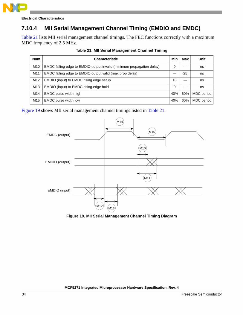
7.10.4 MII Serial Management Channel Timing (EMDIO and EMDC)
Table 21 lists MII serial management channel timings. The FEC functions correctly with a maximum MDC frequency of 2.5 MHz.
Figure 19 shows MII serial management channel timings listed in Table 21.
Figure 19. MII Serial Management Channel Timing Diagram
Table 21. MII Serial Management Channel Timing
Num Characteristic Min Max Unit
M10 EMDC falling edge to EMDIO output invalid (minimum propagation delay) 0 — ns
M11 EMDC falling edge to EMDIO output valid (max prop delay) — 25 ns
M12 EMDIO (input) to EMDC rising edge setup 10 — ns
M13 EMDIO (input) to EMDC rising edge hold 0 — ns
M14 EMDC pulse width high 40% 60% MDC period
M15 EMDC pulse width low 40% 60% MDC period
EMDC (output)
EMDIO (output)
M12M13
EMDIO (input)
M10
M14
M15
M11
MCF5271 Integrated Microprocessor Hardware Specification, Rev. 4
Freescale Semiconductor34
Electrical Characteristics
7.11 32-Bit Timer Module AC Timing SpecificationsTable 22 lists timer module AC timings.
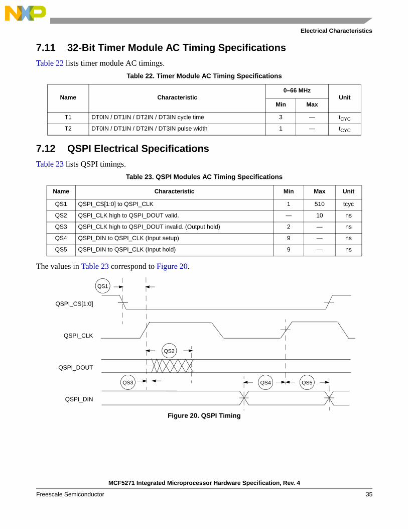
7.12 QSPI Electrical Specifications Table 23 lists QSPI timings.
The values in Table 23 correspond to Figure 20.
Figure 20. QSPI Timing
Table 22. Timer Module AC Timing Specifications
Name Characteristic 0–66 MHz
UnitMin Max
T1 DT0IN / DT1IN / DT2IN / DT3IN cycle time 3 — tCYC
T2 DT0IN / DT1IN / DT2IN / DT3IN pulse width 1 — tCYC
Table 23. QSPI Modules AC Timing Specifications
Name Characteristic Min Max Unit
QS1 QSPI_CS[1:0] to QSPI_CLK 1 510 tcyc
QS2 QSPI_CLK high to QSPI_DOUT valid. — 10 ns
QS3 QSPI_CLK high to QSPI_DOUT invalid. (Output hold) 2 — ns
QS4 QSPI_DIN to QSPI_CLK (Input setup) 9 — ns
QS5 QSPI_DIN to QSPI_CLK (Input hold) 9 — ns
QSPI_CS[1:0]
QSPI_CLK
QSPI_DOUT
QS5
QS1
QSPI_DIN
QS3 QS4
QS2
MCF5271 Integrated Microprocessor Hardware Specification, Rev. 4
Freescale Semiconductor 35
Electrical Characteristics
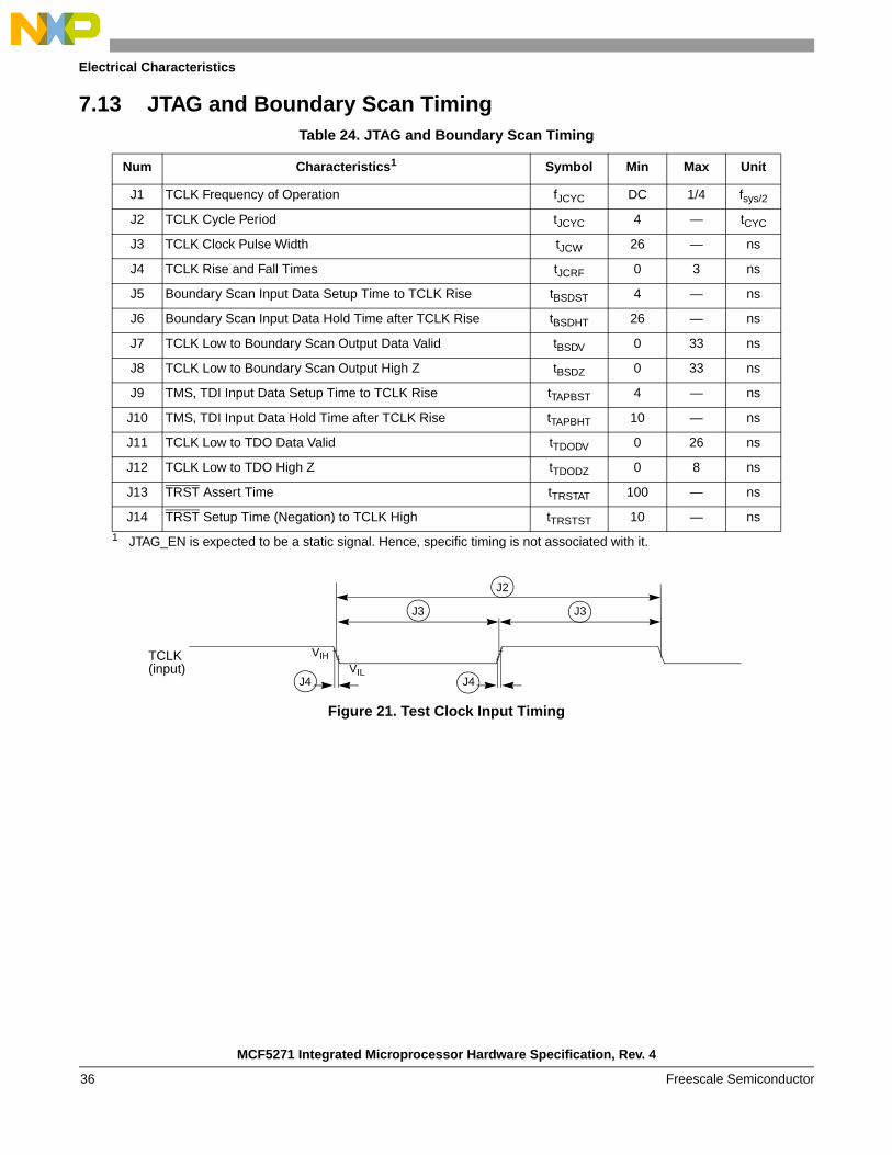
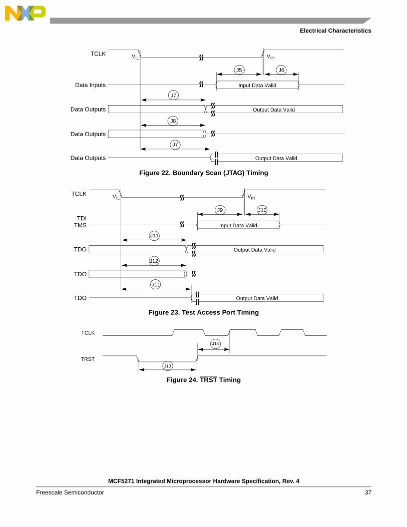
7.13 JTAG and Boundary Scan Timing
Figure 21. Test Clock Input Timing
Table 24. JTAG and Boundary Scan Timing
Num Characteristics1
1 JTAG_EN is expected to be a static signal. Hence, specific timing is not associated with it.
Symbol Min Max Unit
J1 TCLK Frequency of Operation fJCYC DC 1/4 fsys/2
J2 TCLK Cycle Period tJCYC 4 — tCYC
J3 TCLK Clock Pulse Width tJCW 26 — ns
J4 TCLK Rise and Fall Times tJCRF 0 3 ns
J5 Boundary Scan Input Data Setup Time to TCLK Rise tBSDST 4 — ns
J6 Boundary Scan Input Data Hold Time after TCLK Rise tBSDHT 26 — ns
J7 TCLK Low to Boundary Scan Output Data Valid tBSDV 0 33 ns
J8 TCLK Low to Boundary Scan Output High Z tBSDZ 0 33 ns
J9 TMS, TDI Input Data Setup Time to TCLK Rise tTAPBST 4 — ns
J10 TMS, TDI Input Data Hold Time after TCLK Rise tTAPBHT 10 — ns
J11 TCLK Low to TDO Data Valid tTDODV 0 26 ns
J12 TCLK Low to TDO High Z tTDODZ 0 8 ns
J13 TRST Assert Time tTRSTAT 100 — ns
J14 TRST Setup Time (Negation) to TCLK High tTRSTST 10 — ns
TCLKVIL
VIH
J3 J3
J4 J4
J2
(input)
MCF5271 Integrated Microprocessor Hardware Specification, Rev. 4
Freescale Semiconductor36
Electrical Characteristics
Figure 22. Boundary Scan (JTAG) Timing
Figure 23. Test Access Port Timing
Figure 24. TRST Timing
Input Data Valid
Output Data Valid
Output Data Valid
TCLK
Data Inputs
Data Outputs
Data Outputs
Data Outputs
VIL VIH
J5 J6
J7
J8
J7
Input Data Valid
Output Data Valid
Output Data Valid
TCLK
TDI
TDO
TDO
TDO
TMS
VIL VIH
J9 J10
J11
J12
J11
TCLK
TRST
J14
J13
MCF5271 Integrated Microprocessor Hardware Specification, Rev. 4
Freescale Semiconductor 37
Electrical Characteristics
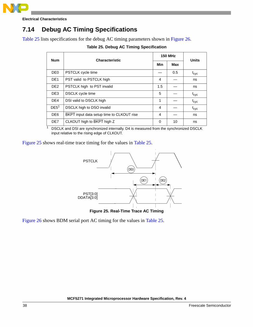
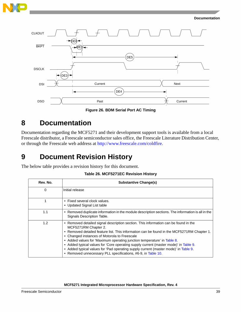
7.14 Debug AC Timing SpecificationsTable 25 lists specifications for the debug AC timing parameters shown in Figure 26.
Figure 25 shows real-time trace timing for the values in Table 25.
Figure 25. Real-Time Trace AC Timing
Figure 26 shows BDM serial port AC timing for the values in Table 25.
Table 25. Debug AC Timing Specification
Num Characteristic150 MHz
UnitsMin Max
DE0 PSTCLK cycle time — 0.5 tcyc
DE1 PST valid to PSTCLK high 4 — ns
DE2 PSTCLK high to PST invalid 1.5 — ns
DE3 DSCLK cycle time 5 — tcyc
DE4 DSI valid to DSCLK high 1 — tcyc
DE51
1 DSCLK and DSI are synchronized internally. D4 is measured from the synchronized DSCLK input relative to the rising edge of CLKOUT.
DSCLK high to DSO invalid 4 — tcyc
DE6 BKPT input data setup time to CLKOUT rise 4 — ns
DE7 CLKOUT high to BKPT high Z 0 10 ns
PSTCLK
PST[3:0]
DE2DE1
DDATA[3:0]
DE0
MCF5271 Integrated Microprocessor Hardware Specification, Rev. 4
Freescale Semiconductor38
Documentation
Figure 26. BDM Serial Port AC Timing
8 DocumentationDocumentation regarding the MCF5271 and their development support tools is available from a local Freescale distributor, a Freescale semiconductor sales office, the Freescale Literature Distribution Center, or through the Freescale web address at http://www.freescale.com/coldfire.
9 Document Revision HistoryThe below table provides a revision history for this document.
Table 26. MCF5271EC Revision History
Rev. No. Substantive Change(s)
0 Initial release
1 • Fixed several clock values. • Updated Signal List table
1.1 • Removed duplicate information in the module description sections. The information is all in the Signals Description Table.
1.2 • Removed detailed signal description section. This information can be found in the MCF5271RM Chapter 2.
• Removed detailed feature list. This information can be found in the MCF5271RM Chapter 1. • Changed instances of Motorola to Freescale • Added values for ‘Maximum operating junction temperature’ in Table 8. • Added typical values for ‘Core operating supply current (master mode)’ in Table 9. • Added typical values for ‘Pad operating supply current (master mode)’ in Table 9. • Removed unnecessary PLL specifications, #6-9, in Table 10.
DSI
DSO
Current Next
CLKOUT
Past Current
DSCLK
DE3
DE4
DE5
BKPT
DE6
DE7
MCF5271 Integrated Microprocessor Hardware Specification, Rev. 4
Freescale Semiconductor 39
Document Revision History
1.3 • Device is now available in 150 MHz versions. Updated specs where necessary to reflect this improvement.
• Added 2 new part numbers to Table 6: MCF5270CVM150 and MCF5271CVM150. • Removed features list. This information can be found in the MCF5271RM. • Removed SDRAM address multiplexing section. This information can be found in the
MCF5271RM.
1.4 • Added Section 5.2.1, “Supply Voltage Sequencing and Separation Cautions.” • Updated 196MAPBGA package dimensions, Figure 4.
2 • Table 2: Changed SD_CKE pin location from 139 to “—” for the 160QFP device. • Table 2: Changed QSPI_CS1 pin location from “—” to 139 for the 160QFP device. • Table 2: Changed DT3IN pin’s alternate 2 function from “—” to QSPI_CS2. • Table 2: Changed DT3OUT pin’s alternate 2 function from “—” to QSPI_CS3. • Figure 5: Changed pin 139 label from “SD_CKE/QSPI_CS1” to “QSPI_CS1/SD_CKE”. • Removed second sentence from Section 7.10.1, “MII Receive Signal Timing (ERXD[3:0],
ERXDV, ERXER, and ERXCLK),” and Section 7.10.2, “MII Transmit Signal Timing (ETXD[3:0], ETXEN, ETXER, ETXCLK),” regarding no minimum frequency requirement for TXCLK.
• Removed third and fourth paragraphs from Section 7.10.2, “MII Transmit Signal Timing (ETXD[3:0], ETXEN, ETXER, ETXCLK),” as this feature is not supported on this device.
3 • Section 5.2.1, “Supply Voltage Sequencing and Separation Cautions” changed PLLVDD to VDDPLL to match rest of document.
• Section 5.2.1, “Supply Voltage Sequencing and Separation Cautions” Changed VDDPLL voltage level from 1.5V to 3.3V throughout section.
• Section 5.2.1.1, “Power Up Sequence” first bullet, changed “Use 1 µs” to “Use 1 ms”. • Corrected position of spec D5 in Figure 11. • Figure 3: Corrected M4 ball location from DATA5 to DATA6, changed DATAn labels to Dn for
consistency • Table 14: Added DACKn and DREQn to footnote. • Table 9, added PLL supply voltage row
4 • Added part number MCF5270CAB100 in Table 6
Table 26. MCF5271EC Revision History (continued)
Rev. No. Substantive Change(s)
MCF5271 Integrated Microprocessor Hardware Specification, Rev. 4
Freescale Semiconductor40
Document Revision History
MCF5271 Integrated Microprocessor Hardware Specification, Rev. 4
Freescale Semiconductor 41
Document Number: MCF5271ECRev. 408/2009
How to Reach Us:
Home Page:www.freescale.com
E-mail:[email protected]
USA/Europe or Locations Not Listed:Freescale SemiconductorTechnical Information Center, CH3701300 N. Alma School RoadChandler, Arizona 85224+1-800-521-6274 or [email protected]
Europe, Middle East, and Africa:Freescale Halbleiter Deutschland GmbHTechnical Information CenterSchatzbogen 781829 Muenchen, Germany+44 1296 380 456 (English)+46 8 52200080 (English)+49 89 92103 559 (German)+33 1 69 35 48 48 (French)[email protected]
Japan:Freescale Semiconductor Japan Ltd.HeadquartersARCO Tower 15F1-8-1, Shimo-Meguro, Meguro-ku,Tokyo 153-0064Japan0120 191014 or +81 3 5437 [email protected]
Asia/Pacific:Freescale Semiconductor Hong Kong Ltd.Technical Information Center2 Dai King StreetTai Po Industrial EstateTai Po, N.T., Hong Kong+800 2666 [email protected]
For Literature Requests Only:Freescale Semiconductor Literature Distribution CenterP.O. Box 5405Denver, Colorado 802171-800-441-2447 or 303-675-2140Fax: [email protected]
Information in this document is provided solely to enable system and software implementers to use Freescale Semiconductor products. There are no express or implied copyright licenses granted hereunder to design or fabricate any integrated circuits or integrated circuits based on the information in this document.
Freescale Semiconductor reserves the right to make changes without further notice to any products herein. Freescale Semiconductor makes no warranty, representation or guarantee regarding the suitability of its products for any particular purpose, nor does Freescale Semiconductor assume any liability arising out of the application or use of any product or circuit, and specifically disclaims any and all liability, including without limitation consequential or incidental damages. “Typical” parameters that may be provided in Freescale Semiconductor data sheets and/or specifications can and do vary in different applications and actual performance may vary over time. All operating parameters, including “Typicals”, must be validated for each customer application by customer’s technical experts. Freescale Semiconductor does not convey any license under its patent rights nor the rights of others. Freescale Semiconductor products are not designed, intended, or authorized for use as components in systems intended for surgical implant into the body, or other applications intended to support or sustain life, or for any other application in which the failure of the Freescale Semiconductor product could create a situation where personal injury or death may occur. Should Buyer purchase or use Freescale Semiconductor products for any such unintended or unauthorized application, Buyer shall indemnify and hold Freescale Semiconductor and its officers, employees, subsidiaries, affiliates, and distributors harmless against all claims, costs, damages, and expenses, and reasonable attorney fees arising out of, directly or indirectly, any claim of personal injury or death associated with such unintended or unauthorized use, even if such claim alleges that Freescale Semiconductor was negligent regarding the design or manufacture of the part.
Freescale™ and the Freescale logo are trademarks of Freescale Semiconductor, Inc. All other product or service names are the property of their respective owners.
© Freescale Semiconductor, Inc. 2009. All rights reserved.
RoHS-compliant and/or Pb-free versions of Freescale products have the functionality and electrical characteristics as their non-RoHS-compliant and/or non-Pb-free counterparts. For further information, see http://www.freescale.com or contact your Freescale sales representative.
For information on Freescale’s Environmental Products program, go to http://www.freescale.com/epp.
Recommended