
General DescriptionThe MAX17558 is a dual-output, synchronous step-down controller that drives nMOSFETs.The device features a peak-current-mode, constant- frequency architecture, allowing it to operate up to 2.2MHz. The device can be configured as two single-phase, independent 10A power supplies or as a dual-phase, single-output 20A power supply. The device also provides the ability to run two controllers 180° out-of-phase to reduce the power loss and noise due to the input-capacitor ESR.The IC supports current sensing using either an external current-sense resistor for accuracy or an inductor DCR for improved system efficiency. Current foldback limits MOSFET power dissipation under short-circuit conditions.The IC provides independent adjustable soft-start for each output and can start up monotonically into a prebiased output. The IC can be configured in either PWM or DCM modes of operation, depending on whether constant-frequency operation or light-load efficiency is desired.The IC operates over the -40°C to +125°C temperature range and is available in a lead(Pb)-free, 32-pin TQFN, 5mm x 5mm package with an exposed pad.
Applications Industrial Power Supplies Distributed DC Power Systems Motion Control Programmable Logic Controllers Computerized Numerical Control
Benefits and Features Wide Range of Operation
• Wide 4.5V to 60V Input Voltage Range• Wide 0.8V to 24V Output Voltage Range• RSENSE or Inductor DCR Current Sensing• Selectable In-Phase or 180° Out-of-Phase
Operation• Adjustable 100kHz to 2.2MHz Switching Frequency• Independent Enable and PGOOD• Available in a Lead(Pb)-Free 32-Pin, 5mm x 5mm
TQFN-EP Package Enhances Power Efficiency
• Low-Impedance Gate Drives for High Efficiency• DCM Operation at Light Loads• Auxiliary Bootstrap LDO
Operates Reliably in Adverse Industrial Environments• Independent Adjustable Soft-Start or Tracking• Current Foldback Limits MOSFET Heat Dissipation
During a Short-Circuit Condition• Operates Over the -40°C to +125°C Temperature
Range• Output Overvoltage and Overtemperature Protections
Ordering Information appears at end of data sheet.
MAX17558 60V, Dual-Output, Synchronous Step-Down Controller
19-7532; Rev 1; 3/16
EVALUATION KIT AVAILABLE

0.88V
VFB1
0.72V0.88V
VFB
2
0.72V
BST_24,17
DH_26,15
25,16LX_
VCCINT
CONTROLLOGIC
DL_23,18
PGND21
FB_31,11
COMP_30,12
SS_29,13
5µA
EA 0.80VSS_
ZX
RS Q
Q
DUPLICATE FOR SECONDCONTROLLER CHANNEL
SLOPECOMP
1.8µA
EN_7,8
10µA2
27
14
SEL_PH3 4
TEST
CLK2
CLK1
OSC
CURRENTLIMIT
LDO
EN
196GND
LDO
EN
4.7V
VCCINT
20VCCEXT
22IN
28ILIM
5SKIP
100K
RT
PGOOD2
PGOOD1
CS_+32,10CS_-1,9
1.5V
SKIP
MAX17558 60V, Dual-Output, Synchronous Step-Down Controller
www.maximintegrated.com Maxim Integrated 2
Block Diagram

IN to GND ..............................................................-0.3V to +70VCS_+ to GND ........................................................-0.3V to +40VCS_+ to CS_- .......................................................-0.3V to +0.3VLX_, BST_ to PGND .............................................-0.3V to +70VBST_ to LX_ ............................................................-0.3V to +6VBST_ to VCCINT ....................................................-0.3V to +70VDH_ to LX_ ............................................-0.3V to (VBST_ + 0.3)VDL_ to PGND ...................................... -0.3V to (VCCINT + 0.3)VEN_ to GND ............................................................-0.3V to +6VVCCINT to GND .......................................................-0.3V to +6VVCCEXT to GND ....................................................-0.3V to +26VPGND to GND ......................................................-0.3V to +0.3V
PGOOD_ to GND ....................................................-0.3V to +6VFB_, COMP_, SS_, RT, SKIP, SEL_PH,
ILIM .................................................. -0.3V to (VCCINT + 0.3)VGND to EP ............................................................-0.3V to +0.3VContinuous Power Dissipation at +70°C
(multilayer board) ....................................................2758.6mWPower Deration (multilayer board) ...........................34.5 mW/°COperating Temperature Range ......................... -40°C to +125°CMaximum Junction Temperature .....................................+150°CStorage Temperature Range ............................ -65°C to +160°CLead Temperature (soldering, 10s) .................................+300°C
Junction-to-Ambient Thermal Resistance (θJA) ..............29°C/W Junction-to-Case Thermal Resistance (θJC) ..................1.7°C/W
(Note 1)
(VIN = 24V, RT = open, CVCCINT = 4.7µF, EN_ = open, DH_, DL_ = open, TJ = -40°C to +125°C, unless otherwise noted. Typical values are at TA = +25°C.) (Note 2)
PARAMETER SYMBOL CONDITIONS MIN TYP MAX UNITS
INPUT SUPPLY
Input Voltage Range VIN4.5 60
VVCCINT = VIN 4.5 5.5
Operating Supply Current (Note 3) IIN
SKIP = open, LX_ = PGND, BST_ = 5V EN1 = open, EN2 = GND, VFB1 = 0.84V or EN2 = open, EN1 = GND, VFB2 = 0.84V
0.5 1.5 2.0mA
SKIP = open, LX_ = PGND, BST_ = 5VEN1 = EN2 = open, VFB1 = VFB1 = 0.84V 1 2.5 3.5
SKIP = VCCINT, LX_ = PGND, BST_ = 5V EN1 = open, EN2 = GND, VFB1 = 0.76V orEN2 = open, EN1 = GND, VFB2 = 0.76V
1 1.8 3.5mA
SKIP = VCCINT, LX_ = PGND,BST_=5V EN1 = EN2 = open, VFB1 = VFB1 = 0.76V 1.5 3.2 5
Shutdown Supply Current EN1 = EN2 = GND 10 20 µA
MAX17558 60V, Dual-Output, Synchronous Step-Down Controller
www.maximintegrated.com Maxim Integrated 3
Note 1: Package thermal resistances were obtained using the method described in JEDEC specification JESD51-7, using a four-layer board. For detailed information on package thermal considerations, refer to www.maximintegrated.com/thermal-tutorial.
Absolute Maximum Ratings
Stresses beyond those listed under “Absolute Maximum Ratings” may cause permanent damage to the device. These are stress ratings only, and functional operation of the device at these or any other conditions beyond those indicated in the operational sections of the specifications is not implied. Exposure to absolute maximum rating conditions for extended periods may affect device reliability.
Package Thermal Characteristics
Electrical Characteristics

(VIN = 24V, RT = open, CVCCINT = 4.7µF, EN_ = open, DH_, DL_ = open, TJ = -40°C to +125°C, unless otherwise noted. Typical values are at TA = +25°C.) (Note 2)
PARAMETER SYMBOL CONDITIONS MIN TYP MAX UNITS
VCCINT REGULATOR
VCCINT Output Voltage VCCINT
6V < VIN < 60V, IVCCINT = 1mA 4.95 5.1 5.25V6V < VCCEXT < 24V, IVCCINT = 1mA
(VCCINT supplied from VCCEXT) 4.95 5.1 5.25
VCCINT Load Regulation
VIN = 12V, I = 0mA to 100mA, VCCEXT = 0V (VCCINT supplied from VIN)
5 25 50mV
VVCCEXT = 12V, IVCCINT = 0mA to 100mA (VCCINT supplied from VCCEXT) 5 25 50
VCCINT Short-Circuit Output Current
VIN = 8.5V, VCCEXT = 0V, VCCINT = 4V 120 250 340mAVCCEXT = 8.5V, VCCINT = 4V
(VCCINT supplied from VCCEXT)120 250 340
VCCINT Dropout VoltageVIN = 4.5V, load = 75mA, VCCEXT = 0 50 150 420
mVVCCINT supplied from VCCEXT, VIN = 24V, VCCEXT = 4.7V, load = 75mA 50 150 420
VCCEXT Switch Overvoltage VCCEXT rising 4.55 4.7 4.85 V
VCCEXT Switch Overvoltage Hysteresis 0.2 0.25 0.3 V
VCCINT UVLOVCCINT rising 4 4.2 4.4
VVCCINT falling 3.5 3.7 3.9
OSCILLATOR
Switching Frequency fSW
RT = 62kΩ 405 440 475
kHzRT = VCCINT 480 535 590
RT = GND 325 350 375
RT Pullup Current VRT = 0.5V 9.5 10 10.5 µA
Switching Frequency Adjustable Range fSW 26.5kΩ < RT < 280kΩ 100 2200 kHz
SKIP
DCM Mode Setting Range 1.25 VCCINT -1.6
V
PWM Mode Setting Range VCCINT - 1.5
VCCINT V
SKIP Pulldown Resistance 70 100 130 kΩ
MAX17558 60V, Dual-Output, Synchronous Step-Down Controller
www.maximintegrated.com Maxim Integrated 4
Electrical Characteristics (continued)

(VIN = 24V, RT = open, CVCCINT = 4.7µF, EN_ = open, DH_, DL_ = open, TJ = -40°C to +125°C, unless otherwise noted. Typical values are at TA = +25°C.) (Note 2)
PARAMETER SYMBOL CONDITIONS MIN TYP MAX UNITS
GATE DRIVER
DH_ to BST_ On-Resistance Sourcing 100mA 0.7 1.3 2.5 Ω
DH_ to LX_ On-Resistance Sinking 100mA 0.25 0.5 0.9 Ω
DL_ to VCCINT On-Resistance Sourcing 100mA 0.7 1.3 2.5 Ω
DL_ to PGND_ On-Resistance Sinking 100mA 0.35 0.75 1.25 Ω
DH_ Minimum Controlled On-Time tON_MIN 120 155 ns
DL_ Minimum Controlled Off-Time tOFF_MIN PWM mode, VFB_ = 0.84V 80 120 160 ns
Dead Time tDTDH_ falling to DL_ rising, CLOAD = 6nF 30
nsDL_ falling to DH_ rising, CLOAD = 6nF 30
DH_ Transition TimeDH_ rising, CLOAD = 6nF 25
nsDH_ falling, CLOAD = 6nF 15
DL_ Transition TimeDL_ rising, CLOAD = 6nF 25
nsDL_ falling, CLOAD = 6nF 15
SOFT-START
Soft-Start Current ISS VSS = 0.5V 3.5 5 6.5 µA
ENABLE
EN_ Logic-High Threshold EN_ rising 1.2 1.25 1.3 V
EN_ Hysteresis 90 mV
EN_ Bias Pullup Bias Current VEN_ = 0.5V 0.9 1.8 2.7 µA
CURRENT-SENSE AMPLIFIER
CS_+ , CS_- Common-Mode Voltage Range 0 24 V
CS_+ to CS_- Input Operating Voltage Range
VCS_+ -VCS_-
0 < VCS_- < 24V -100 +100 mV
Current-Sense Amplifier Gain
ILIM = GND 30 33.3 36.6
V/VILIM = open 18 20 22
VILIM = VCCINT 12 13.3 14.5
CS_+ Input Bias Current 0 < VCS_- < 24V, TA = TJ = +25°C 0.01 1 µA
CS_- Input Bias Current VCS_+ = VCS_- = 1.2V or 24V 5 600 µA
MAX17558 60V, Dual-Output, Synchronous Step-Down Controller
www.maximintegrated.com Maxim Integrated 5
Electrical Characteristics (continued)

(VIN = 24V, RT = open, CVCCINT = 4.7µF, EN_ = open, DH_, DL_ = open, TJ = -40°C to +125°C, unless otherwise noted. Typical values are at TA = +25°C.) (Note 2)
Note 2: Limits are 100% tested at TA = +25°C. Limits over the temperature range and relevant supply voltage range are guaranteed by design and characterization.
Note 3: This supply current excludes the switching current due to the external MOSFETs’ gate charge.
PARAMETER SYMBOL CONDITIONS MIN TYP MAX UNITS
CURRENT LIMIT
Cycle-by-Cycle Peak Positive Current-Limit Threshold VCS
ILIM = open, VIN = 12V, VOUT = 1.25V 42.5 50 55
mVILIM = GND, VIN = 12V, VOUT = 1.25V 23 30 37
VILIM = VCCINT, VIN = 12V, VOUT = 1.25V 65 75 85
ERROR AMPLIFIER
Feedback Regulation Voltage VFB_ 788 800 812 mV
FB _ Input Leakage Current VFB_ = 0.8V, TA = TJ = +25°C -100 0 +100 nA
Transconductance gM_ 1.7 2 2.3 mA/V
POWER-GOOD OUTPUTS
PGOOD_ ThresholdVFB__rising 103 110 113 % of
FB_VFB__falling 87 90 93
PGOOD_ Output Low Level IPGOOD_ = 10mA 0.05 0.15 0.25 V
PGOOD_ Leakage Current VPGOOD_= 5V , TA = TJ = +25°C -100 +100 nA
THERMAL SHUTDOWN
Thermal-Shutdown Threshold 160 °C
Thermal-Shutdown Hysteresis 20 °C
MAX17558 60V, Dual-Output, Synchronous Step-Down Controller
www.maximintegrated.com Maxim Integrated 6
Electrical Characteristics (continued)
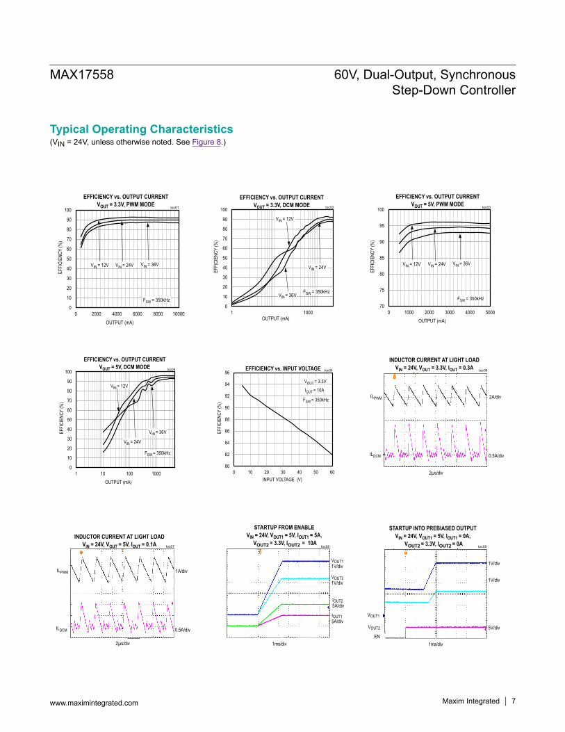
(VIN = 24V, unless otherwise noted. See Figure 8.)
0
10
20
30
40
50
60
70
80
90
100
1 1000
EFFI
CIEN
CY (%
)
OUTPUT (mA)
EFFICIENCY vs. OUTPUT CURRENTVOUT = 3.3V, DCM MODE toc02
VIN = 12V
VIN = 24V
VIN = 36V FSW = 350kHz
70
75
80
85
90
95
100
0 1000 2000 3000 4000 5000
EFFI
CIEN
CY(%
)
OUTPUT (mA)
EFFICIENCY vs. OUTPUT CURRENTVOUT = 5V, PWM MODE toc03
VIN = 12V VIN = 24V VIN = 36V
FSW = 350kHz
0
10
20
30
40
50
60
70
80
90
100
1 10 100 1000
EFFI
CIEN
CY (%
)
OUTPUT (mA)
EFFICIENCY vs. OUTPUT CURRENTVOUT = 5V, DCM MODE toc04
VIN = 12V
VIN = 24V
VIN = 36V
FSW = 350kHz
80
82
84
86
88
90
92
94
96
0 10 20 30 40 50 60
EFFI
CIEN
CY (%
)
INPUT VOLTAGE (V)
EFFICIENCY vs. INPUT VOLTAGE toc05
IOUT = 10A
FSW = 350kHz
VOUT = 3.3V
INDUCTOR CURRENT AT LIGHT LOADVIN = 24V, VOUT = 3.3V, IOUT = 0.3A toc06
2µs/div
ILPWM
0.5A/div
2A/div
ILDCM
INDUCTOR CURRENT AT LIGHT LOADVIN = 24V, VOUT = 5V, IOUT = 0.1A toc07
2µs/div
ILPWM
0.5A/div
1A/div
ILDCM
0
10
20
30
40
50
60
70
80
90
100
0 2000 4000 6000 8000 10000
EFFI
CIEN
CY(%
)
OUTPUT (mA)
EFFICIENCY vs. OUTPUT CURRENTVOUT = 3.3V, PWM MODE toc01
VIN = 12V VIN = 24V VIN = 36V
FSW = 350kHz
STARTUP FROM ENABLEVIN = 24V, VOUT1 = 5V, IOUT1 = 5A,
VOUT2 = 3.3V, IOUT2 = 10Atoc08
1ms/div
IOUT15A/div
IOUT25A/div
VOUT21V/div
VOUT11V/div
STARTUP INTO PREBIASED OUTPUTVIN = 24V, VOUT1 = 5V, IOUT1 = 0A,
VOUT2 = 3.3V, IOUT2 = 0A toc09
1ms/div
5V/div
1V/div
1V/div
VOUT1
EN
VOUT2
MAX17558 60V, Dual-Output, Synchronous Step-Down Controller
Maxim Integrated 7www.maximintegrated.com
Typical Operating Characteristics

(VIN = 24V, unless otherwise noted. See Figure 8.)
COINCIDENT TRACKING AT STARTUPVIN = 24V, VOUT1 = 5V, IOUT1 = 5A,
VOUT2 = 3.3V, IOUT2 = 10A toc10
1ms/div
5A/div
1V/div
1V/divVOUT1
IOUT2
VOUT2
5A/div
IOUT1
LOAD TRANSIENT RESPONSEVIN = 24V, VOUT2 = 3.3V, IOUT2 = 0.1A to 5A
DCM MODE toc11
200µs/div
2A/div
100mV/divAC-COUPLED
IOUT2
VOUT2
LOAD TRANSIENT RESPONSEVIN = 24V, VOUT2 = 3.3V, IOUT2 = 0A to 5A
PWM MODE toc12
200µs/div
2A/div
50mV/divAC-COUPLED
IOUT2
VOUT2
LOAD TRANSIENT RESPONSEVIN = 24V, VOUT2 = 3.3V, IOUT2 = 5A to 10A
PWM MODE toc13
200µs/div
5A/div
50mV/divAC-COUPLED
I
VOUT2
OUT2
LOAD TRANSIENT RESPONSEVIN = 24V, VOUT1 = 5V, IOUT1 = 0.05A to 2.5A
DCM MODE toc14
200µs/div
1A/div
100mV/divAC-COUPLED
IOUT1
VOUT1
LOAD TRANSIENT RESPONSEVIN = 24V, VOUT1 = 5V, IOUT1 = 0A to 2.5A
PWM MODE toc15
200µs/div
1A/div
50mV/divAC-COUPLED
IOUT1
VOUT1
LOAD TRANSIENT RESPONSEVIN = 24V, VOUT1 = 5V, IOUT1 = 2.5A to 5A
PWM MODE toc16
200µs/div
2A/div
50mV/divAC-COUPLED
IOUT1
VOUT1
OVERCURRENT PROTECTIONVIN = 24V, VOUT2 = 3.3V, IOUT2 = SHORT
PWM MODE toc17
40µs/div
1V/div
IOUT2
VOUT2
5A/div
OVER CURRENT PROTECTIONVIN = 24V, VOUT1 = 5V, IOUT1 = SHORT
PWM MODE toc18
20µs/div
2V/div
IOUT1
VOUT1
2A/div
MAX17558 60V, Dual-Output, Synchronous Step-Down Controller
Maxim Integrated 8www.maximintegrated.com
Typical Operating Characteristics (continued)

(VIN = 24V, unless otherwise noted. See Figure 8.)
SHORT-CIRCUIT UNDER STEADY-STATEVIN = 24V, VOUT1 = 5V, IOUT2 = 5A TO SHORT
PWM MODE toc20
20µs/div
2V/div
IOUT1
VOUT1
2A/div
-150
-120
-90
-60
-30
0
30
60
90
120
150
1k 10k 100k-50
-40
-30
-20
-10
0
10
20
30
40
50
PHAS
E MA
RGIN
(°)
GAIN
(dB)
FREQUENCY (Hz)
CLOSED-LOOP BODE PLOTVIN = 24V, VOUT = 5V, IOUT = 5A
GAIN
toc27
PHASE
CROSSOVER FREQUENCY = 39kHzPHASE MARGIN = 64.9
-150
-120
-90
-60
-30
0
30
60
90
120
150
1k 10k 100k-50
-40
-30
-20
-10
0
10
20
30
40
50
PHAS
E MA
RGIN
(°)
GAIN
(dB)
FREQUENCY (Hz)
CLOSED-LOOP BODE PLOTVIN = 24V, VOUT = 3.3V, IOUT = 10A
GAIN
toc28
PHASE
CROSSOVER FREQUENCY = 39.8kHzPHASE MARGIN = 69°
0° IN-PHASE OPERATIONVIN = 36V, VOUT1 = 24V, IOUT2 = 0A
VOUT2 = 3.3V, IOUT2 = 0A, PWM MODE toc29
1µs/div
20V/div
20V/divLX1
LX2
180° OUT-OF-PHASE OPERATIONVIN = 36V, VOUT1 = 24V, IOUT2 = 0A
VOUT2 = 3.3V, IOUT2 = 0A, PWM MODE toc30
1µs/div
20V/div
20V/divLX1
LX2
SHORT-CIRCUIT UNDER STEADY-STATEVIN = 24V, VOUT2 = 3.3V, IOUT2 = 10A TO SHORT
PWM MODE toc19
10µs/div
2V/div
IOUT2
VOUT2
5A/div
MAX17558 60V, Dual-Output, Synchronous Step-Down Controller
Maxim Integrated 9www.maximintegrated.com
Typical Operating Characteristics (continued)

(VIN = 24V, unless otherwise noted. See Figure 8.)
MAX17558 60V, Dual-Output, Synchronous Step-Down Controller
Maxim Integrated 10www.maximintegrated.com
Typical Operating Characteristics (continued)
5
5.03
5.06
5.09
5.12
5.15
5.18
0 20 40 60
V CCI
NTVO
LTAG
E(V
)
INPUT VOLTAGE (V)
VCCINT VOLTAGEvs. INPUT VOLTAGE toc21
-5
45
95
145
195
245
0 5 10 15 20
CS-P
ININ
PUT
BIAS
CURR
ENT
(µA)
VSENSE COMMON MODE VOLTAGE (V)
CS_- PIN INPUT BIAS CURRENTvs. VSENSE COMMON-MODE VOLTAGE
0
10
20
30
40
50
60
70
80
90
100
0 0.2 0.4 0.6 0.8 1
MAXI
MUM
CURR
ENT-
SENS
EVO
LTAG
E(m
V)
FEEDBACK VOLTAGE (V)
MAXIMUM CURRENT-SENSE VOLTAGEvs. FEEDBACK VOLTAGE
toc23
ILIM = GND
ILIM = OPEN
ILIM = VCCINT
0
30
60
90
120
150
180
210
240
-45 -20 5 30 55 80 105 130
CS_-
PIN
INPU
T CU
RREN
T (µ
A)
TEMPERATURE (°C)
CS_- PIN INPUT CURRENTvs. TEMPERATURE
toc24
VOUT = 3.3V
VOUT = 24V
0
100
200
300
400
500
600
-45 -20 5 30 55 80 105 130
SWIT
CHIN
G FR
EQUE
NCY
(kHz)
TEMPERATURE (°C)
SWITCHING FREQUENCYvs. TEMPERATURE
RT = GND
RT = VCCINT
4.7
4.75
4.8
4.85
4.9
4.95
5
5.05
5.1
5.15
5.2
0 25 50 75 100
V CCIN
TVO
LTAG
E (V
)
VCCINT LOAD CURRENT (mA)
VCCINT LOAD REGULATION
VCCEXT = 12V, VIN = 24V
VCCEXT = 0V, VIN = 24V
VCCEXT = 5V, VIN = 12V

MAX17588
TQFN(5mm x 5mm)
TOP VIEW
29
30
28
27
12
11
13
RT
TEST
SKIP
GND
EN1
14
CS1-
DL1
PGND
V CCE
XT
BST1
V CCI
NT
DL2
1 2
ILIM
4 5 6 7
2324 22 20 19 18
SS1
COMP1
PGOOD2
SS2
COMP2
FB2SE
L_PH
IN
3
21
31 10FB1 CS2+
32 9CS1+ CS2-+
PGOOD1
26 15 DH2DH1
25 16 LX2
EN2
BST2
8
17
LX1
PIN NAME FUNCTION
1, 9 CS1-, CS2- Current-Sense Amplifier Negative Input of Controller 1 and Controller 2, Respectively. Connect to negative terminal of current-sense signal. See Figure 5 and Figure 6.
2 RTSwitching-Frequency Programming Resistor Connection. Connect a resistor between RT and GND to set the switching frequency. See Figure 3. Connect to VCCINT to program switching frequency of 535kHz. Connect to GND to program switching frequency of 350kHz.
3 SEL_PH Phase-Selection Input. The SEL_PH pin programs the phase shift between the two controllers of the device.
4 TEST Connect to GND
5 SKIPConnect SKIP to VCCINT to select PWM mode of operation. Pull up SKIP with 100kΩ to VCCINT or connect to a voltage between 1.25V and VCCINT - 1.5V to program DCM mode of operation. SKIP is internally pulled down to GND by 100kΩ.
6 GND Signal Ground Connection. GND should connect to the PGND plane at a single point. Refer to the MAX17558 evaluation kit data sheet PCB layout for an example grounding scheme.
7, 8 EN1, EN2Enable Input for Controller 1 and Controller 2. Either leave unconnected or connect to a voltage between 1.25V and 5.5V to enable corresponding controller. Connect to GND to disable corresponding controller.
MAX17558 60V, Dual-Output, Synchronous Step-Down Controller
www.maximintegrated.com Maxim Integrated 11
Pin Description
Pin Configuration

PIN NAME FUNCTION
10, 32 CS2+, CS1+ Current-Sense Amplifier Positive Input of Controller 2 and Controller 1. Connect to positive terminal of current-sense signal. See Figure 5 and Figure 6.
11, 31 FB2, FB1 Feedback Voltage Input of Controller 2 and Controller 1. Connect the FB_ pins to the midpoint of a resistor-divider from output to GND. See the circuit of Figure 4 for details.
12, 30 COMP2, COMP1
Error-Amplifier Output and Compensation Network-Connection Node for Controller 2 and Controller 1. Connect the COMP_ pins to the compensation network as shown in the circuit of Figure 7.
13, 29 SS2, SS1
Output-Voltage Soft-Start Time Programming Pins. Connect a capacitor from SS_ to GND to program output-voltage soft-start time. Alternatively, a resistor-divider on another voltage supply connected to this pin allows the device output to track the other supply during startup. See the Shutdown and Startup (EN_ and SS_) and Soft-Start Capacitor sections for more details.
14, 27 PGOOD2, PGOOD1
Open-Drain Power-Good Pins of Controller 2 and Controller 1. Pull up with external resistor to a maximum of 5.5V.
15, 26 DH2, DH1 High-Side MOSFET Gate-Driver Output of Controller 2 and Controller 1. Connect to gate of respective high-side MOSFET.
16, 25 LX2, LX1 Switching Node Connection Input of Controller 2 and Controller 1. Connect to respective output-filter inductors.
17, 24 BST2, BST1 Bootstrap Capacitor Connection Input of Controller 2 and Controller 1. Connect a capacitor between BST_ and corresponding LX_. See the Bootstrap Capacitor Selection section for more details.
18, 23 DL2, DL1 Low-Side MOSFET Gate-Driver Output of Controller 2 and Controller 1. Connect to gate of respective low-side MOSFET.
19 VCCINTInternal LDO Output. Connect a minimum 4.7µF low-ESR ceramic capacitor between VCCINT and PGND.
20 VCCEXT
External Power-Supply Input for Internal LDO. Apply a voltage between 4.85V and 24V to disconnect the LDO that operates from IN, and power internal circuitry with the LDO connected to VCCEXT. A minimum of 0.1µF local decoupling for the VCCEXT pin is recommended.
21 PGNDPower Ground. Connect to the source terminal of the external low-side MOSFETs and VCCINT bypass capacitor return terminal. Refer to the MAX17558 evaluation kit data sheet PCB layout for an example.
22 IN Supply Input. Bypass with minimum 1µF low-ESR ceramic capacitor to PGND.
28 ILIM Current-Limit Selection Input for Both Controllers. See the Peak Current-Limit Programming (ILIM) section for a more detailed description.
— EPExposed Pad. Connect to GND pin of the IC. Connect to a large copper plane with multiple vias to improve thermal performance. Refer to the MAX17558 evaluation kit data sheet PCB layout for an example grounding scheme and thermal via arrangement.
MAX17558 60V, Dual-Output, Synchronous Step-Down Controller
www.maximintegrated.com Maxim Integrated 12
Pin Description (continued)

Detailed DescriptionThe MAX17558 is a dual-output synchronous step-down controller that operates from a 4.5V to 60V wide input supply range with programmable output volt-age ranging from 0.8V to 24V. The IC uses constant- frequency, peak current-mode control for the control loop. The frequency of the device can be adjusted from 100kHz to 2.2MHz using a resistor at the RT pin. Input capacitor size can be minimized by running the two outputs 180° out-of-phase.The phase shift between the two controllers of the IC can be selected using the SEL_PH pin. The device provides independent adjustable soft-start and can start up monotonically with a prebiased output voltage. It also features selectable DCM/PWM mode of operation. Other features include independent open-drain PGOOD_ outputs and independent enable (EN_) inputs.
Internal LDO (VCCINT)The IC has two internal 100mA low-dropout (LDO) linear regulators that power VCCINT. One regulator is powered from IN, while the other is powered from VCCEXT. At any time, one of the two regulators is in operation depending on the voltage levels at VCCEXT. If VCCEXT voltage is greater than 4.7V (typ) then VCCINT is powered from the VCCEXT regulator. If VCCEXT is lower than 4.55V (typ), then VCCINT is powered from the IN regulator. Powering VCCINT from VCCEXT increases efficiency at higher input voltages. VCCEXT can be connected to one of the switch-ing regulator outputs if that output voltage is greater than 4.7V (typ). The maximum voltage limit on VCCEXT is 24V.VCCINT output voltage powers the gate drivers and internal control circuitry. VCCINT should be decoupled to PGND with at least a 4.7µF low-ESR ceramic capacitor. The IC employs an undervoltage-lockout (UVLO) circuit that forces both the regulators off when VCCINT falls below 3.8V (typ). The regulators are enabled again when VCCINT > 4.2V (typ).
Low-Side Gate Driver (DL_)Low-side external MOSFET gate drivers are powered from VCCINT. Under normal operating conditions, the low-side gate-driver output (DL_) is always the complement of the high-side gate-driver output (DH_). On each controller, dedicated circuitry monitors the DH_ and DL_ outputs and prevents either gate-drive signal from turning on until the other gate-drive signal is fully off. Thus, the circuit allows DH_ to turn on only when DL_ has been turned off. Similarly, it prevents DL_ from turning on until DH_ has been turned off.There must be a low-impedance path from the DL_ and DH_ pins to the external MOSFET gates to ensure that the gate driver’s circuitry works properly. To minimize impedance, very short, wide traces should be used in the PCB layout. The internal pulldown transistor that drives the DL_ low is robust with a 0.75Ω (typ) on-resistance. This low on-resistance helps prevent DL_ from being pulled up during the fast rising of the LX_ node, due to capacitive coupling from the drain to the gate of the low-side synchronous rectifier MOSFET.
High-Side Gate Driver (DH_)High-side gate drivers are powered from the bootstrap capacitors connected between BST_ and LX_. The boot-strap capacitor normally gets charged to VCCINT during each switching cycle through an external Schottky diode, when the low-side MOSFET turns on.The high-side MOSFET is turned on by closing an internal switch between BST_ and DH_. This provides the necessary gate-to-source voltage to turn on the high-side MOSFET. See the Bootstrap Capacitor Selection section to choose the right size of the bootstrap capacitor.
MAX17558 60V, Dual-Output, Synchronous Step-Down Controller
www.maximintegrated.com Maxim Integrated 13
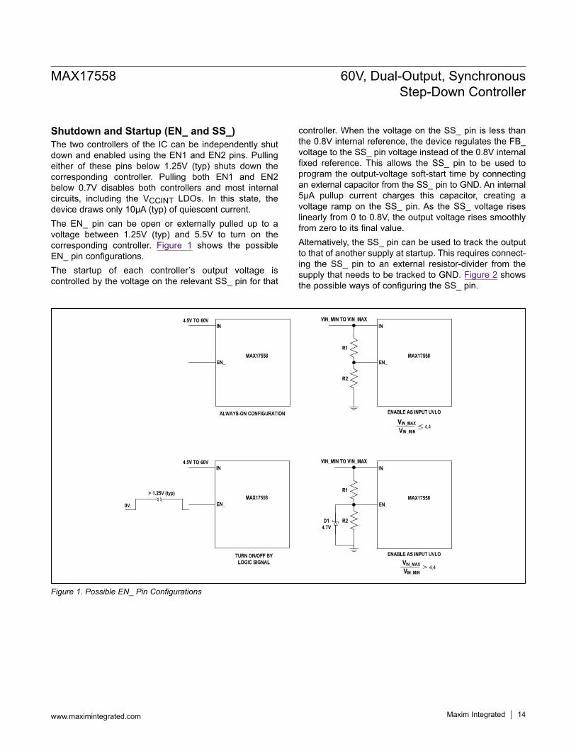
Shutdown and Startup (EN_ and SS_)The two controllers of the IC can be independently shut down and enabled using the EN1 and EN2 pins. Pulling either of these pins below 1.25V (typ) shuts down the corresponding controller. Pulling both EN1 and EN2 below 0.7V disables both controllers and most internal circuits, including the VCCINT LDOs. In this state, the device draws only 10µA (typ) of quiescent current.The EN_ pin can be open or externally pulled up to a voltage between 1.25V (typ) and 5.5V to turn on the corresponding controller. Figure 1 shows the possible EN_ pin configurations.The startup of each controller’s output voltage is controlled by the voltage on the relevant SS_ pin for that
controller. When the voltage on the SS_ pin is less than the 0.8V internal reference, the device regulates the FB_ voltage to the SS_ pin voltage instead of the 0.8V internal fixed reference. This allows the SS_ pin to be used to program the output-voltage soft-start time by connecting an external capacitor from the SS_ pin to GND. An internal 5µA pullup current charges this capacitor, creating a voltage ramp on the SS_ pin. As the SS_ voltage rises linearly from 0 to 0.8V, the output voltage rises smoothly from zero to its final value.Alternatively, the SS_ pin can be used to track the output to that of another supply at startup. This requires connect-ing the SS_ pin to an external resistor-divider from the supply that needs to be tracked to GND. Figure 2 shows the possible ways of configuring the SS_ pin.
Figure 1. Possible EN_ Pin Configurations
MAX17558 60V, Dual-Output, Synchronous Step-Down Controller
www.maximintegrated.com Maxim Integrated 14

Figure 2. Possible SS_ Pin Configurations
SS2
SS1
MAX17588
INDEPENDENT SOFT-START
VOUT1
VOUT2
OUTPUTVOLTAGE
TIME
R3
R4
MAX17588
SS2
DH1 VOUT1
DL1
PGND
SS1
VOUT1 FB1
R1
R2DL2
DH2
VOUT2
VIN
VIN
FB2
R3
R4
R1
R2
MAX17588
SS2
DH1 VOUT1
DL1
PGND
SS1
VOUT1 FB1
R1
R2DL2
DH2
VOUT2
VIN
VIN
FB2
R3
R4
COINCIDENT TRACKING
VOUT1
VOUT2
OUTPUTVOLTAGE
TIME
RATIOMETRIC TRACKING
VOUT1
VOUT2
OUTPUTVOLTAGE
TIME
MAX17558 60V, Dual-Output, Synchronous Step-Down Controller
www.maximintegrated.com Maxim Integrated 15
Light-Load Current Operation (SKIP)The MAX17558 can be configured to operate either in discontinuous-conduction (DCM) mode for high light-load efficiency or fixed-frequency pulse-width-modulation (PWM) mode. To select DCM mode of operation, connect the SKIP pin to a DC voltage between 1.25V and VCCINT - 1.5V. To select PWM mode of operation, connect SKIP to VCCINT.
DCM ModeIn DCM mode, the IC turns off the low-side MOSFET of the regulator close to the zero-crossing of the inductor current in each switching cycle. This operation minimizes negative current in the inductor, reducing loss due to current flowing from the output to the input. Therefore, the inductor current in each cycle is a triangular waveform whose peak is proportional to the load current demand. The controller operates at a constant frequency while adjusting the peak current in the inductor for load and input-voltage variations. However, under light-load and/or high input-voltage conditions, there exists a minimum on-time constraint for the controller. The minimum on-time is the smallest controllable pulse width that the controller can generate. This imposes a lower limit on the peak inductor current that can be programmed in the inductor and causes a fixed amount of energy to be delivered to the output, regardless of the energy requirement of the load. If the load is such that the amount of energy delivered during minimum on-time is more than the load energy, the output voltage rises above its nominal set value. This results in skipping of switching cycles to regulate the average output voltage to the set point. This operation results in an effective switching frequency that is lower than the programmed switching frequency, which improves the regulator efficiency. As the load current increases to a point where the valley of the inductor current rises above zero, the regulator operation moves into PWM mode.
PWM ModeEach controller of the device operates in PWM mode whenever SKIP is connected to VCCINT. The inductor current is allowed to go negative in this mode. In PWM mode, under normal operating conditions, the high-side MOSFET turns on at an edge of the internal clock. An internal error amplifier compares the feedback voltage at the FB_ pin to a fixed internal reference voltage and gen-erates an error current. This error current flows through the compensation network at the COMP_ pin and gener-ates control voltage for the inner current loop. The on-time of the high-side MOSFET in a switching cycle is deter-mined by comparing the control voltage at the COMP_ pin with the sum of the current-sense voltage at CS_+,
CS_-, and the internal slope-compensation voltage. The inductor current ramps up during high-side MOSFET turn-on time. Once the high-side MOSFET is turned off, the low-side MOSFET is turned on. During low-side MOSFET turn-on time, the inductor current ramps down. The low-side MOSFET remains on until the next clock edge. PWM mode of operation has the advantages of low output-voltage ripple and constant-frequency operation, which is beneficial in applications that are sensitive to operating frequency. Under minimum on-time conditions described in the DCM Mode section, the device skips high-side turn-on events in PWM mode also, to regulate the output voltage. This results in low-frequency operation with regard to inductor current and output-voltage-ripple waveforms.
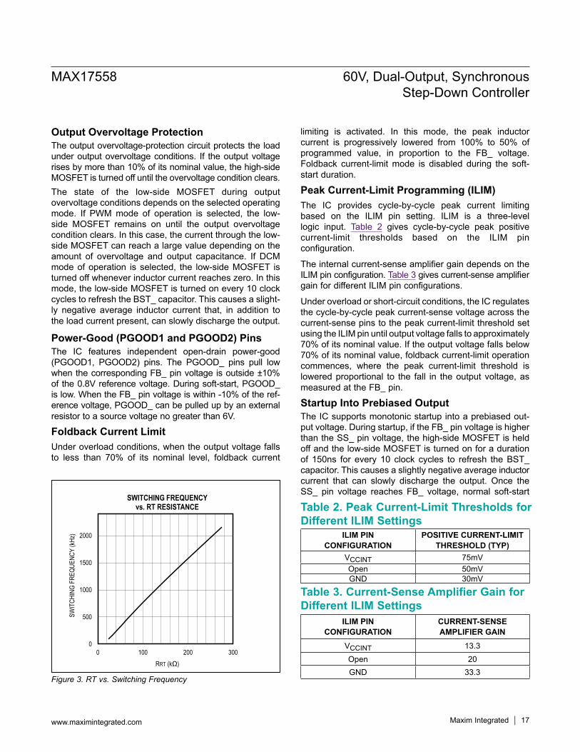
Frequency Selection (RT)The selection of switching frequency is a tradeoff between efficiency and component size. Low-frequency operation increases efficiency by reducing MOSFET switching losses and gate-drive losses, but requires a larger inductor and/or capacitor to maintain low output-ripple voltage. The switching frequency of the device can be programmed between 100kHz and 2.2MHz using the RT pin. Connect RT to VCCINT to program a default frequency of 535kHz switching frequency, and to GND to program 350kHz switching frequency. Figure 3 shows the switching frequency for different RT values.The following formula can be used to find the required resistor for a given switching frequency.
RTR =fSW + 133
8.8
0 to 180° Phase OperationThe IC allows the user to configure the phase shift between the two output channels of the device. Table 1 gives selecta-ble phase-shift configurations based on SEL_PH.The advantages of operation with 180° phase shift between channels are:
Reduction of input and output capacitor RMS current. Lower input-voltage ripple.
Table 1. Configuring Phase Shift Using SEL_PH
SEL_PH LX1/LX2 PHASING
VCCINT 0°/0°
Open 0°/180°
MAX17558 60V, Dual-Output, Synchronous Step-Down Controller
www.maximintegrated.com Maxim Integrated 16
Output Overvoltage ProtectionThe output overvoltage-protection circuit protects the load under output overvoltage conditions. If the output voltage rises by more than 10% of its nominal value, the high-side MOSFET is turned off until the overvoltage condition clears.The state of the low-side MOSFET during output overvoltage conditions depends on the selected operating mode. If PWM mode of operation is selected, the low-side MOSFET remains on until the output overvoltage condition clears. In this case, the current through the low-side MOSFET can reach a large value depending on the amount of overvoltage and output capacitance. If DCM mode of operation is selected, the low-side MOSFET is turned off whenever inductor current reaches zero. In this mode, the low-side MOSFET is turned on every 10 clock cycles to refresh the BST_ capacitor. This causes a slight-ly negative average inductor current that, in addition to the load current present, can slowly discharge the output.
Power-Good (PGOOD1 and PGOOD2) PinsThe IC features independent open-drain power-good (PGOOD1, PGOOD2) pins. The PGOOD_ pins pull low when the corresponding FB_ pin voltage is outside ±10% of the 0.8V reference voltage. During soft-start, PGOOD_ is low. When the FB_ pin voltage is within -10% of the ref-erence voltage, PGOOD_ can be pulled up by an external resistor to a source voltage no greater than 6V.
Foldback Current LimitUnder overload conditions, when the output voltage falls to less than 70% of its nominal level, foldback current
limiting is activated. In this mode, the peak inductor current is progressively lowered from 100% to 50% of programmed value, in proportion to the FB_ voltage. Foldback current-limit mode is disabled during the soft-start duration.
Peak Current-Limit Programming (ILIM)The IC provides cycle-by-cycle peak current limiting based on the ILIM pin setting. ILIM is a three-level logic input. Table 2 gives cycle-by-cycle peak positive current-limit thresholds based on the ILIM pin configuration.
The internal current-sense amplifier gain depends on the ILIM pin configuration. Table 3 gives current-sense amplifier gain for different ILIM pin configurations.
Under overload or short-circuit conditions, the IC regulates the cycle-by-cycle peak current-sense voltage across the current-sense pins to the peak current-limit threshold set using the ILIM pin until output voltage falls to approximately 70% of its nominal value. If the output voltage falls below 70% of its nominal value, foldback current-limit operation commences, where the peak current-limit threshold is lowered proportional to the fall in the output voltage, as measured at the FB_ pin.
Startup Into Prebiased OutputThe IC supports monotonic startup into a prebiased out-put voltage. During startup, if the FB_ pin voltage is higher than the SS_ pin voltage, the high-side MOSFET is held off and the low-side MOSFET is turned on for a duration of 150ns for every 10 clock cycles to refresh the BST_ capacitor. This causes a slightly negative average inductor current that can slowly discharge the output. Once the SS_ pin voltage reaches FB_ voltage, normal soft-start
Figure 3. RT vs. Switching Frequency
Table 2. Peak Current-Limit Thresholds for Different ILIM Settings
Table 3. Current-Sense Amplifier Gain for Different ILIM Settings
0
500
1000
1500
2000
0 100 200 300
SWIT
CHIN
G FR
EQUE
NCY
(kHz)
RRT (kΩ)
SWITCHING FREQUENCYvs. RT RESISTANCE
ILIM PIN CONFIGURATION
POSITIVE CURRENT-LIMIT THRESHOLD (TYP)
VCCINT 75mVOpen 50mVGND 30mV
ILIM PIN CONFIGURATION
CURRENT-SENSE AMPLIFIER GAIN
VCCINT 13.3Open 20GND 33.3
MAX17558 60V, Dual-Output, Synchronous Step-Down Controller
www.maximintegrated.com Maxim Integrated 17

operation occurs, and the output voltage smoothly ramps up from the prebiased value.
Operating Input Voltage RangeFor a step-down converter, the minimum and maximum operating input voltages for a given output voltage should be calculated as follows:
VIN_MIN =
+ ILOAD(MAX) x (RDS(ON)_HI - RDS(ON)_LOW)
VOUT + ILOAD(MAX) x (RDS(ON)_LOW + DCR)1 - fSW_MAX x tOFF_MIN
VIN_MAX =VOUT
(fSW_MAX x tON_MIN)
where VOUT is the steady-state output voltage, ILOAD(MAX) is the maximum load current, DCR is the DC resistance of the inductor, fSW_MAX is the maximum switching frequency, RDS(ON)_HI are the on-state resistances of the high-side and low-side MOSFETs, tOFF_MIN is the worst-case minimum off-time (160ns), and tON_MIN is the worst-case minimum on-time (155ns) from the Electrical Characteristics table.
Thermal-Overload ProtectionThermal-overload protection limits total power dissipation in the IC. When the junction temperature of the device exceeds +160°C, an on-chip thermal sensor shuts down the device, allowing it to cool. The thermal sensor turns the device on again after the junction temperature cools by 20°C. The device restarts with soft-start when recovering from thermal shutdown.
Applications InformationSetting the Input Undervoltage-Lockout LevelThe EN_ pins can be used as input undervoltage-lockout detectors with a typical hysteresis of 100mV. As shown in Figure 1, the input voltage at which each controller of the IC turns on, can be set with a resistor-divider connected to corresponding EN_ from IN to GND.Select R2 = 10kW and calculate R1 based on the following equation:
1.25R1 = R2 x(VINUVLO - 1.25)
where VINUVLO is the input voltage at which the controller should be enabled.
Setting the Output VoltageThe output voltage of each controller is set by connecting a resistor-divider to FB_ from the corresponding output to GND (Figure 4). Select R1 using the following equation, based on the offset introduced on the output voltage by the FB_ leakage. Let α be the offset introduced on the output voltage:
FB_R1
Iα
≤
where IFB_ is the FB_ leakage current (±100nA max). For example, for VOUT = 5V, α = 0.1% of VOUT (= 5mV).
5mVR10.1µA
≤
R1 ≤ 50kΩCalculate R2 with the following equation:
OUT
R1R 2V
10.8
=
−
Figure 4. Output-Voltage Programming
MAX17588FB_
VOUT_
R1
R2
MAX17558 60V, Dual-Output, Synchronous Step-Down Controller
www.maximintegrated.com Maxim Integrated 18

Soft-Start CapacitorSoft-start time is programmed by connecting a capacitor from the SS_ pin to GND. An internal 5µA current source charges the capacitor at the SS_ pins providing a linear ramping voltage for output-voltage reference. The soft-start time is calculated based on the following equation:
SS SS0.8Vt C5µA
= ×
Inductor SelectionThree key inductor parameters must be specified to select output inductor:1) Inductance (L).2) Inductor saturation current (ISAT).3) DC resistance of inductor (DCR).The required inductance (L) is calculated based on the ratio of inductor peak-to-peak ripple AC current to its DC average current (LIR). A good compromise between size and loss is a 30% peak-to-peak ripple current to average-current ratio (LIR = 0.3). The switching frequency, input voltage, output voltage, and selected LIR then determine the inductor value as follows:
OUT
LOAD SW
V (1 D)L
LIR I f× −
=× ×
where VOUT is the output voltage, D is the operating duty cycle (= VOUT/VIN), ILOAD is the full-load current, and fSW is the operating switching frequency.The minimum inductor saturation current should be equal to or greater than maximum inductor peak current given by the following equation:
Maximum InductorPeak Current Maximum Load Current + ΔILPK-PK (max)=
where ΔILPK-PK(max) is the maximum inductor ripple current and can be calculated as follows:
OUTOUT
INMAXLPK PK
SW
VV 1
VI
L f−
× − D×
(max) =
Selecting an inductor with lower DCR improves efficiency, but there is a lower limit for DCR based on the minimum peak-to-peak current-sense signal required at the current-sense pins, as described in the Current Sensing (CS_+ and CS_-) section.
Current Sensing (CS_+ and CS_-)The CS_+ and CS_- pins are the inputs to the internal current-sense amplifiers. The common-mode operating voltage range on these pins is 0 to 24V, enabling the IC to regulate output voltages up to a nominal 24V.Whether the current sensing is done by an external current-sense resistor or inductor DCR, the desired current-sense resistance is calculated using the following equation:
CSSENSE
LPK PKLOAD(MAX)
VR
I (max)I
2
=+ -
where:RSENSE is the desired current-sense resistor,VCS is the selected current-limit threshold based on ILIM pin setting,ILOAD(MAX) is the maximum load current.To ensure that the application delivers full-load current over the full operating temperature range, select the minimum value for the VCS parameter from the Electrical Characteristics table.It should be noted that the magnitude of current-sense ripple voltage is critical for a good signal-to-noise ratio to ensure minimum duty-cycle jitter. The worst-case current-sense ripple voltage occurs at minimum operating input voltage, and should be set in the 7mV to 12mV range. The following equation can be used to calculate the worst-case current-sense ripple voltage at the CS_+, CS_- pins:
CSmin LPK PK SENSEV I (min) R−D = D ×
where ΔILPK-PK(min) is the minimum inductor current ripple, which occurs at minimum operating input voltage. ΔILPK-PK(min) can be calculated using the following equation:
OUTOUT
INMINLPK PK
SW
VV 1V
I (min)L f−
× − D =×
MAX17558 60V, Dual-Output, Synchronous Step-Down Controller
www.maximintegrated.com Maxim Integrated 19
If DVCSMIN is less than the target value, the selected output inductance should be lowered, and RSENSE should be iteratively recalculated until DVCSMIN is equal to or greater than the target value (7mV to 10mV, depending on PCB layout), and VCSMAX, as calculated by the following equation is less than the selected VCS from the Electrical Characteristics table.
LPK PKCSMAX SENSE LOADMAX
I (max)2
−D = × + V R I
Because of PCB layout-related noise, operation at the minimum operating voltage should be checked for jitter before finalizing the worst-case current-sense voltage. Care should be taken to ensure that current-sense filter components should be placed close to the IC’s current-sense pins. The current-sense traces should be short and differentially routed.
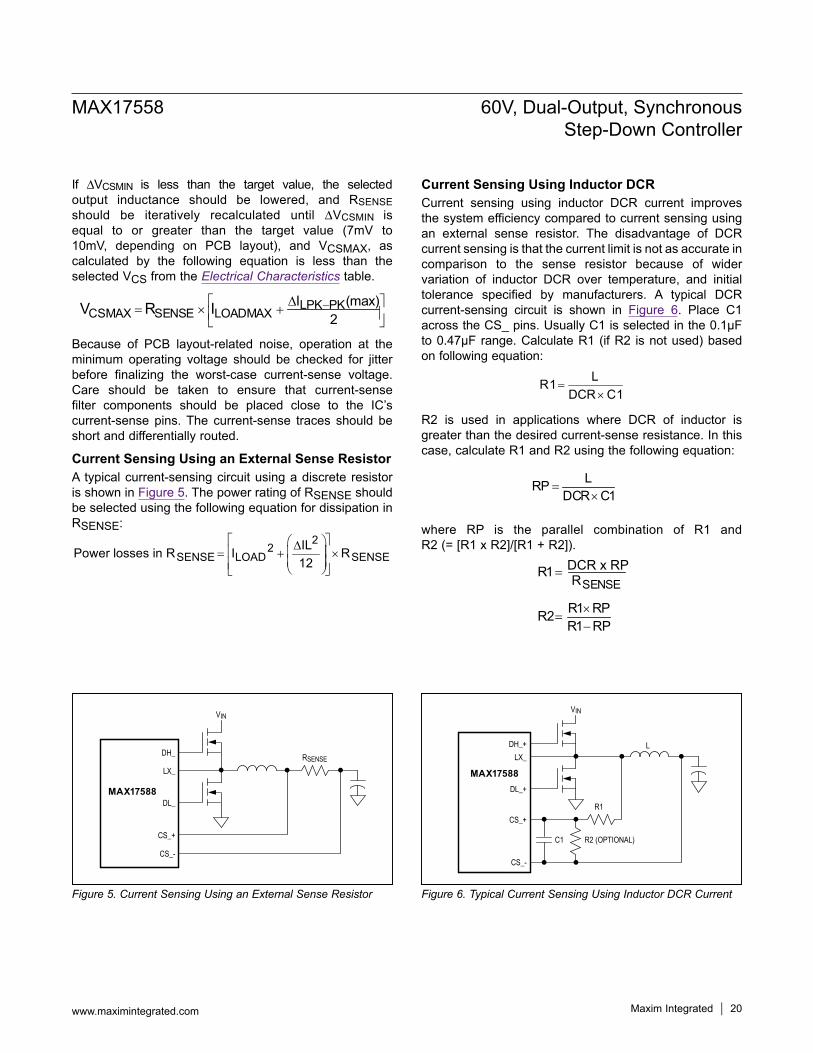
Current Sensing Using an External Sense ResistorA typical current-sensing circuit using a discrete resistor is shown in Figure 5. The power rating of RSENSE should be selected using the following equation for dissipation in RSENSE:
22
SENSE LOAD SENSEILPower losses in R I R12
D = + ×
Current Sensing Using Inductor DCRCurrent sensing using inductor DCR current improves the system efficiency compared to current sensing using an external sense resistor. The disadvantage of DCR current sensing is that the current limit is not as accurate in comparison to the sense resistor because of wider variation of inductor DCR over temperature, and initial tolerance specified by manufacturers. A typical DCR current-sensing circuit is shown in Figure 6. Place C1 across the CS_ pins. Usually C1 is selected in the 0.1µF to 0.47µF range. Calculate R1 (if R2 is not used) based on following equation:
LR1DCR C1
=×
R2 is used in applications where DCR of inductor is greater than the desired current-sense resistance. In this case, calculate R1 and R2 using the following equation:
LRPDCR C1
=×
where RP is the parallel combination of R1 and R2 (= [R1 x R2]/[R1 + R2]).
R1 DCR x RPSENSER
R2
=
= R1 RPR1 RP
×−
Figure 5. Current Sensing Using an External Sense Resistor Figure 6. Typical Current Sensing Using Inductor DCR Current
MAX17588
DH_
DL_
LX_
CS_+
CS_-
RSENSE
VIN
MAX17588
DH_+
DL_+
LX_
CS_+
C1 R2 (OPTIONAL)
CS_-
L
R1
VIN
MAX17558 60V, Dual-Output, Synchronous Step-Down Controller
www.maximintegrated.com Maxim Integrated 20

Input Capacitor SelectionThe input filter capacitor reduces peak currents drawn from the power source and reduces noise and voltage ripple on the input caused by the circuit’s switching. Use low-ESR ceramic capacitors at the input. For each output channel, calculate the input capacitance required for a specified input-ripple DVIN using the following equations, by neglecting the ripple component due to ESR of input capacitor:
LOADIN
SW
I D (1 D)CVIN
× × −=
η×D × f
where D = (VOUT/VIN), E is efficiency of power conversion. The input capacitor RMS current requirement (CINRMS) can be calculated by the following equation:
RMS LOAD(MAX)CIN I D (1 D)= × × −
where ILOAD(MAX) is the maximum value of load current, D = VOUT/VIN.
Output Capacitor SelectionThe key selection parameters for the output capacitor are capacitance value, ESR, and voltage rating. These parameters affect the overall stability, output-ripple voltage, and transient response. The steady-state output ripple (ΔVOUTSS) has two components (by neglecting the ESL of the output capacitors): one component is due to the voltage drop across the ESR (ΔVOUTESR_SS) and the other component is due to the variation in charge stored in the output capacitor (ΔVOUTQ_SS). By neglecting the output-voltage drop due to ESL of output capacitor, approx-imate output voltage ripple under steady state is given by:
OUTSS OUTESR _SS OUTQ _SSV V VD ≈ D + D
where ΔVOUTSS is the output-voltage ripple under steady state:
OUTESR _SS PK PK
PK PKOUTQ _SS
SW OUT
V IL ESR
ILV8 f C
−
−
D = D ×
DD =
× ×
Calculate the required COUT and ESR based on the above equations. For ceramic output capacitors, VOUTQ_SS contributes to approximately 80% of the total output-ripple voltage, ΔVOUTQSS_SS. For electrolytic output capacitors, ΔVOUTQ_SS contributes approximately 50% of the total output-voltage ripple. Low-ESR capacitors should be used.
Loop CompensationThe IC uses an internal transconductance error amplifier with its inverting input and output available to the user for external frequency compensation. The output capacitor and compensation network determine the loop stability for a given output inductor and output capacitor.The controller uses a peak current-mode control scheme that regulates the output voltage by forcing the required current through the external inductor. Current-mode control eliminates the double pole in the feedback loop caused by the inductor and output capacitor in the case of voltage-mode control, resulting in a smaller phase shift and requiring less elaborate error-amplifier compensation.Typical type-2 compensation used with peak current-mode control is shown in Figure 7. Calculate the compensation resistor (RZ) using the following equation:
CO OUT CS SENSEZ
M FB
2 f C G RR
g G× π× × × ×
=×
where:fCO is the desired crossover frequency that should be chosen between fSW/10 and fSW/20,COUT is the output capacitance,GCS is the current-sense amplifier gain, which depends on the ILIM setting,RSENSE is the effective current-sense resistor across the CS_+ and CS_- pins,gM is the internal transconductance amplifier gain,GFB is the output-voltage feedback divider gain, which is equal to (0.8V/output voltage).CZ is calculated using the following equation:
ZP_Load Z
1C2 f R
=× π× ×
where FP_Load is the load-pole frequency approximated by the following equation:
P_LoadOUT
OUTLOAD
1fV
2 CI
=
× π× ×
Calculate CF using the following equation:
FZ P_EA
1C2 R f
=× π× ×
MAX17558 60V, Dual-Output, Synchronous Step-Down Controller
www.maximintegrated.com Maxim Integrated 21
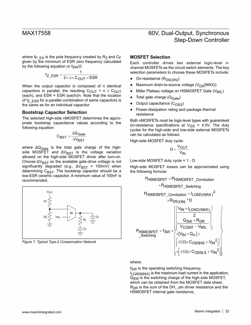
where fP_EA is the pole frequency created by RZ and CF given by the minimum of ESR zero frequency calculated by the following equation or fSW/2:
Z_ESROUT
1f2 C ESR
=× π× ×
When the output capacitor is composed of n identical capacitors in parallel, the resulting COUT = n O COUT (each), and ESR = ESR (each)/n. Note that the location of fZ_ESR for a parallel combination of same capacitors is the same as for an individual capacitor.
Bootstrap Capacitor SelectionThe selected high-side nMOSFET determines the appro-priate bootstrap capacitance values according to the following equation:
GateBST
BST
QC
VD
=D
where ΔQGate is the total gate charge of the high-side MOSFET and ΔVBST is the voltage variation allowed on the high-side MOSFET driver after turn-on. Choose ΔVBST so the available gate-drive voltage is not significantly degraded (e.g., ΔVBST = 100mV) when determining CBST. The bootstrap capacitor should be a low-ESR ceramic capacitor. A minimum value of 100nF is recommended.
MOSFET SelectionEach controller drives two external logic-level n- channel MOSFETs as the circuit switch elements. The key selection parameters to choose these MOSFETs include:
On-resistance (RDS(ON)) Maximum drain-to-source voltage (VDS(MAX)) Miller Plateau voltage on HSMOSFET Gate (VMIL) Total gate charge (QGate) Output capacitance (COSS) Power-dissipation rating and package thermal
resistanceBoth nMOSFETs must be logic-level types with guaranteed on-resistance specifications at VGS = 4.5V. The duty cycles for the high-side and low-side external MOSFETs can be calculated as follows:High-side MOSFET duty cycle:
OUT
IN
VD
V=
Low-side MOSFET duty cycle = 1 - DHigh-side MOSFET losses can be approximated using the following formula:
HSMOSFET HSMOSFET _Conduction
HSMOSFET _Switching2
HSMOSFET_Conduction LOAD(MAX )
DS ON
IN LOAD(MAX)
SW DRCCINT TH_
HSMOSFET SWIN rr_Switching
2OSSHS IN
OS
P PP
P IR *D
V I2
Q RV V
P fV Q
2/3 C V
4/3 C
=
+
=
×
× ××
− = ×
+ × +
× ×
+ × 2SLS INV
×
MIL
(1/2)
(1/2)
where:fSW is the operating switching frequency, ILOAD(MAX) is the maximum load current in the application, QSW is the switching charge of the high-side MOSFET, which can be obtained from the MOSFET data sheet, RDR is the sum of the DH_ pin driver resistance and the HSMOSFET internal gate resistance,
Figure 7. Typical Type-2 Compensation Network
VOUT
R1
R2RZ
gM
CZ
VFB_ CF
MAX17558 60V, Dual-Output, Synchronous Step-Down Controller
www.maximintegrated.com Maxim Integrated 22

VMIL- VGS on HSMOSFET gate that produces IDS = ILOAD(MAX)Qrr is the reverse-recovery charge of low-side MOSFET body diode (if external Schottky is not placed across low-side MOSFET),COSSHS is the effective output capacitance of the high-side MOSFET,COSSLS is the effective output capacitance of the low-side MOSFET.Low-side MOSFET losses can be approximated using the following formula:
2HSMOSFET LOAD(MAX) DS ONP I R 1 D= × × −
+ VD x ILOAD(MAX) x tDT x fSW
where VD is the forward-drop of the LSMOSFET body diode and tDT is the dead time from the Electrical Characteristics table.Take the RDS(ON) variation with temperature into account while calculating the above losses and ensure that the losses of each MOSFET do not exceed their power rat-ing. Using a low Qrr Schottky diode across the low-side MOSFET reduces the high-side MOSFET losses.
Power Dissipation within the MAX17558Gate-charge losses are dissipated by the drivers. Therefore, the gate-driver current taken from the internal LDO regulator and resulting power dissipation must be checked. If VCCEXT is not used to power VCCINT, calculate the approximate IC losses as follows:
MAX17558 IN Gate SW INP V (Q f ) I= × × +
If VCCEXT is used to power the VCCINT, use the following equation to calculate the approximate IC losses:
MAX17558 CCEXT Gate SW INP V (Q f ) I= × × +
where:QGate = Total gate charge of high-side and low-side MOSFETs of controller1 + total gate charge of high-side and low-side MOSFETs of controller 2,IIN is the supply current given in the Electrical Characteristics table.Calculate the IC junction temperature using the following equation and ensure that this value does not exceed +125°C:
J MAX17558 JA AT P Rth T= × +
where:TJ is the IC junction temperature,PMAX17558 is the power losses in the IC,RthJA is the IC junction-to-ambient thermal resistance, which is typically 29°C/W for a multilayer board,TA is the maximum ambient temperature.
PCB Layout GuidelinesCareful PCB layout is critical to achieve low losses, low output noise, and clean and stable operation. Use the following guidelines for PCB layout:
Keep input bypass capacitors as close as possible across the drain of the high-side MOSFET and source of the low-side MOSFET.
If external Schottky diodes are used across the low-side MOSFET, keep the Schottky very close and right across the low-side MOSFET.
Keep IN, VCCINT, VCCEXT bypass capacitors and BST_ capacitors nearer to IC pins.
Route high-speed switching nodes (BST_, LX_, DH_, and DL_) away from the sensitive analog areas (RT, COMP_, CS_, and FB_).
The gate current traces must be short and wide. Use multiple small vias to route these signals if routed from one layer of the PCB to another layer.
Route current-sense lines parallel, short, and next to each other to minimize the loop formed by these lines.
Keep current-sense filter capacitors nearer to IC current-sense pins and on the same side of the IC.
Group all GND-referred and feedback components close to the IC.
Keep the FB_ and compensation-network nets as small as possible to prevent noise pickup.
If possible, place all power components on the top side of the board and run the power-stage currents using traces or copper fills on the top side only, without adding vias.
Keep the power traces and load connections short. This practice is essential for high efficiency. Use thick copper PCBs (2oz or higher) to enhance efficiency and minimize trace inductance and resistance.
On the top side, lay out a large PGND copper area for the output and connect the bottom terminals of the input bypass capacitors, output capacitors, and the source terminals of the low-side MOSFET to that area.
Refer to the MAX17558 evaluation kit data sheet PCB layout for an example.
MAX17558 60V, Dual-Output, Synchronous Step-Down Controller
www.maximintegrated.com Maxim Integrated 23

Figure 8. Wide-Input Voltage, High-Efficiency 5V and 3.3V Output Buck Converter with Resistor-Based Current Sensing (R8, R9).
CS1-
RT
SEL_PH
TEST
SKIP
GND
EN1EN2
CS2-
CS2+
FB2
COMP
2
SS2
PGOO
D2DH
2
LX2
BST2
DL2
V CCI
NT
V CCE
XT
PGND
IN
DL1
BST1
DH1
LX1
PGOO
D1ILIM
COMP
1
SS1
FB1
CS1+
Q1
Q2
Q3
Q4
V OUT
1
V CCI
NT
CS1+
CS1-
VCCI
NT
VCCINT
CS2+
CS2-
VOUT1
VOUT1
MAX17558
PGOO
D1
C7120µF6.3V
C8 C910µF10V
C141µF100V
C151µF
C16
C21C22
C25
C26
L1
L2
R8
R9
R7
R5
R1
R2
R6
R3
R14
R4
C17
C18
10µF
12nF68pF
1nF
1nF
0.47µF
0.47µF
8mΩ
5mΩ
2.2Ω
95.3kΩ
18.2kΩ
53.6kΩ
100kΩ for DCM0Ω for PWM
2.2Ω
4.7µH
2.2µH
C23
C24R10
12nF120pF
V OUT
2
R12
R13
102kΩ
32.4kΩ
PGOO
D2
10µF10V
CS1+
CS1-
C10180µF6.3V
C12 C1310µF10V
10µF10V
C11180µF6.3V
VOUT2
15nF Q5
5V at5A
3.3V at10A
15nFC19
C20
V CCI
NT
R1110kΩ
0.5W
1W
6V to 60V
VIN
CS2+
CS2-
C3
2.2µFC22.2µF
C12.2µF
C52.2µFC6
2.2µFC4
2.2µF
VIN
Q1, Q3, Q5: RJK0651DPBQ2, Q4: RJK0653DPBL1:744771004 , Wurth ElectronicsL2:7447709002 , Wurth ElectronicsC7: EEF-SX0J121E7C10, C11: EEF-SE0J181RD1, D2: Diodes Incorporated DFLS 1100-7
13.3kΩ
12.1kΩ
D1
D2
VCCINT
VCCINT
REFER TO FIGURE 1FOR SETTING UP
EN1, EN2AS UVLO INPUTS
VIN
VOUT1
10kΩ
VOUT2
MAX17558 60V, Dual-Output, Synchronous Step-Down Controller
www.maximintegrated.com Maxim Integrated 24
Typical Application Circuits

Figure 9. Wide Input Voltage, High-Efficiency 5V and 3.3V Output Buck Converter with Inductor DCR Current Sensing (L1, L2).
CS1-
RT
SEL_PH
TEST
SKIP
GND
EN1EN2
CS2-
CS2+
FB2
COMP
2
SS2
PGOO
D2DH
2
LX2
BST2
DL2
V CCI
NT
V CCE
XT
PGND
IN
DL1
BST1
DH1
LX1
PGOO
D1ILIM
COMP
1
SS1
FB1
CS1+
Q1
Q2
Q3
Q4
V OUT
1
V CCI
NT
CS1 P
C S1N
V CC I
NT
VCCINT
CS2P
CS2N
VOUT1
VOUT1
MAX17558
PGOO
D1
C7120µF6.3V
C8 C910µF10V
C141µF100V
C151µF
C16
C21C22
C25
C26
L1
L2
R7
R5
R1
R2
R6
R3
R14
R4
C17
C18
10µF
12nF68pF
100nF
100nF
0.47µF
0.47µF
2.2Ω
95.3kΩ
18.2kΩ
53.6kΩ
100kΩ for DCM0Ω for PWM
2.2Ω
4.7µH
2.2µH
C23
C24R10
12nF120pF
V OUT
2
R12
R13
102kΩ
32.4kΩ
P GOO
D2
10µF10V
CS1P
CS1N
C10180µF6.3V
C12 C1310µF10V
10µF10V
C11180µF6.3V
VOUT2
VOUT2
15nF Q5
5V at5A
3.3V at10A
15nFC19
C20
V CCI
NT
R1110kΩ
6V to 60V
VIN
CS2P
CS2N
C32.2µF
C22.2µF
C12.2µF
C52.2µFC6
2.2µFC4
2.2µF
VIN
Q1, Q3, Q5: RJK0651DPBQ2, Q4: RJK0653DPBL1:744771004 , Wurth ElectronicsL2:7447709002 , Wurth ElectronicsC7: EEF-SX0J121E7C10, C11: EEF-SE0J181RD1, D2: Diodes Incorporated DFLS 1100-7
13.3kΩ
12.1kΩ
D1
D2
VCCINT
VCCINT
REFER TO FIGURE 1FOR SETTING UP
EN1, EN2AS UVLO INPUTS
VIN
VOUT1
10kΩ
R9 3.6kΩ
R8 4.7kΩ
MAX17558 60V, Dual-Output, Synchronous Step-Down Controller
www.maximintegrated.com Maxim Integrated 25
Typical Application Circuits (continued)

Figure 10. Wide Input Voltage, High-Efficiency Dual Phase 3.3V, 20A Output Buck Converter with Resistor-based Current Sensing
R110
0kΩ
R232
. 4kΩ
R312
.1kΩ
C21
12nF
C22
120p
F
FB1
COMP
1SS
1
C19
15nF
ILIM
VOUT
VCCI
NT
R410
kΩ VC
CINTPG
OOD1 VC
CEXT
R5 2.2kΩ
VCCE
XTPG
OOD1
VCCI
NT
C15
1µF
C16
10µF
CS1+
C25
1µF
CS1+
CS1-
RT
R653
.6kΩ
SEL _
PH
TEST
VOUT
R14
100k
Ω F
OR D
CM0Ω
FOR
PW
M
CS1-
GND
EN1
EN2
REFE
R TO
FIG
URE
1 FOR
SE
TTIN
G UP
EN1
,EN2
AS
UVLO
INPU
TS
C14
1µF
100V
IN
VIN
R7 0Ω
BST1
D1VC
CINT
DH1
Q1
C3 4.7µF
C2 4.7µF
C1 4.7µF
C27
4.7µF
VIN
Q6
LX1
DL1
C17
0.47µ
F L1
2.2µH
CS1+
R8 5mΩ
1W
CS1-
PGND
Q2C2
918
0µF
6.3V
C7 180µ
F6.3
V
+C8 10
µF10
V
+C9 10
µF10
V
+
VOUT
VOUT
DL2
Q4L2
2.2µH
LX2
R9 5mΩ
1WVO
UT3.3
V@20
A
CS2+
CS2-
+ +
C10
180µ
F6.3
V
+
C11
180µ
F6.3
V
C12
10µF
10V
C13
10µF
10V VO
UT
BST2
C18
0.47µ
F D2VC
CINT
Q3Q5
C6 4.7µF
C5 4.7µF
C4 4.7µF
C28
4.7µF VI
N
DH2
CS2-
C26
1nF
CS2-
CS2+
FB2
CS2+
FB1
COMP
2
COMP
1
SS2
SS1
PGOO
D2
R11
10KΩ
PGOO
D2VC
CINT
MA
X175
58
Q1, Q
3, Q5
, Q6:
RJK0
651D
PBQ2
, Q4:
RJK0
653D
PBL1
:7447
7100
4, W
URTH
ELE
CTRO
NICS
L2:74
4770
9002
, WUR
TH E
LECT
RONI
CSC7
, C10
, C11
, C29
: EEF
-SE0
J181
RD1
, D2:
DIOD
ES IN
CORP
ORAT
ED D
FLS
1100
-7
4.5V
TO 60
V
R10
69.8k
Ω
MA
X175
52
C30
1µF
IN EN/U
VLO
RT/S
YNC
SS MODE
L310
0µH
LX
GND
VOUT
R3 22.1Ω
FB
R13
324Ω
R12
324Ω
C3
110
µF
RESE
T
VCCE
XTVI
N
MAX17558 60V, Dual-Output, Synchronous Step-Down Controller
www.maximintegrated.com Maxim Integrated 26
Typical Application Circuits (continued)

PART TEMP RANGE BUMP-PACKAGE
MAX17558ATJ+ -40°C to +125°C 32 TQFN-EP*(5mm x 5mm)
PACKAGE TYPE
PACKAGE CODE
OUTLINE NO.
LAND PATTERN NO.
32 TQFN T3255+4 21-0140 90-0012
MAX17558 60V, Dual-Output, Synchronous Step-Down Controller
www.maximintegrated.com Maxim Integrated 27
Package InformationFor the latest package outline information and land patterns (foot-prints), go to www.maximintegrated.com/packages. Note that a “+”, “#”, or “-” in the package code indicates RoHS status only. Package drawings may show a different suffix character, but the drawing pertains to the package regardless of RoHS status.
Ordering Information
Chip InformationPROCESS: BiCMOS
+Denotes a lead(Pb)-free/RoHS-compliant package.*EP = Exposed pad.

REVISIONNUMBER
REVISIONDATE DESCRIPTION PAGES
CHANGED0 3/15 Initial release —1 3/16 Updated General Description and added Typical Application Circuit 1, 26
Maxim Integrated cannot assume responsibility for use of any circuitry other than circuitry entirely embodied in a Maxim Integrated product. No circuit patent licenses are implied. Maxim Integrated reserves the right to change the circuitry and specifications without notice at any time. The parametric values (min and max limits) shown in the Electrical Characteristics table are guaranteed. Other parametric values quoted in this data sheet are provided for guidance.
Maxim Integrated and the Maxim Integrated logo are trademarks of Maxim Integrated Products, Inc.
MAX17558 60V, Dual-Output, Synchronous Step-Down Controller
© 2016 Maxim Integrated Products, Inc. 28
Revision History
For pricing, delivery, and ordering information, please contact Maxim Direct at 1-888-629-4642, or visit Maxim Integrated’s website at www.maximintegrated.com.
Recommended


![· 2 WWW#balJXfgdY#^db#XcZ#]^_[‘bdXkcbJ^dl_[gf][\lfef_lm\dYfX_lm\dYfX#Zel L /+J ˛. ˚ M WWW#‘feZal[^aYa#]^_Ebc]a_kWkf^eac\[Xk‘feZcdlldYk9kD0_DE_9DDEk89A9A8F L ˜ J](https://img.pdfslide.us/doc/110x75/5e11bb1ca7bda8630e6793cf/2-wwwbaljxfgdydbxczabdxkcbjdlgflfeflmdyfxlmdyfxzel-l-j-.jpg)