NXP and the NXP logo are trademarks of NXP B.V. All other product or service names are the property
of their respective owners. © 2017 NXP B.V.
PUBLIC
APPLICATION ENGINEER
BRETISLAV, ZUCZEK
MAGNIV BASED HIGH
CURRENT 3PHS MOTOR
CONTROL SOLUTIONS
AMF-AUT-T2658 | JUNE 2017

PUBLIC 1
AGENDA• Introduction
• HC PCB Design – Considerations
• NXP MC High Current Solution
• MAGNIV Development Board Performance
• MAGNIV Development Board Features
• 2017 Outlook
• Conclusion

PUBLIC 2
Introduction
01.
PUBLIC 3
Motivation
• Missing low voltage high current h/w solution for MC applications in range <20V/
75..100Arms
• New development platform for high current applications:
low end EPS
engine cooling fan
fuel/oil/water pumps
• Reference design targeting customer requirements on high efficiency, high current,
low EMI, good thermal performance
• Customer request for high efficient high current board based on S12ZVM

PUBLIC 4
Design Challenges & Issues
• Optimized MOSFET half bridge switching performance
• Minimize output voltage ringing caused by high rate of current change [di/dt] and parasitic components
(RLC) of the MOSFET packages, PCB traces
• Protect the MCU from damage caused by overvoltage on analogue power pins
• Tradeoff between speed of switching and EMC
• Thermal performance
• PCB manufacturing technology
• Cooling using passive heat-sink
• Price
• Optimize schematic and PCB layout such as to achieve required performance while keeping cost of
manufacturing as low as possible

PUBLIC 5
Project evolution• 1st Generation
Standard six layer stack-up PCB with increased cooper weight to 70um.
• 2nd Generation
Optimized layout regarding to the trace inductance
Standard four layer stack-up PCB with extended tin areas
• 3rd Generation
ICBERG PCB technology used to extend PCB current capability and thermal performance
Standard PCB material FR4
Varying copper thickness on one layer to increase current carrying capability of PCB traces
Updated layout, shorted MOSFET gate control signals
Small compact design

PUBLIC 6
HC PCB Design - Considerations02.

PUBLIC 7
PCB Traces Inductance
• All traces, pads and vias on PCB have some parasitic resistance, inductance and
capacitance (with respect to other traces/vias/planes)
• Inductance of a trace can be directly reduced by:
increased cross-sectional area of the trace
decreased length of the trace
• Thickness of PCB trace is limited, hence increasing cross-sectional area usually
means making the traces wider (plates)
parallel plate vs. coplanar plate
XX

PUBLIC 8
Power Inverter – High Current Path
PUBLIC 9
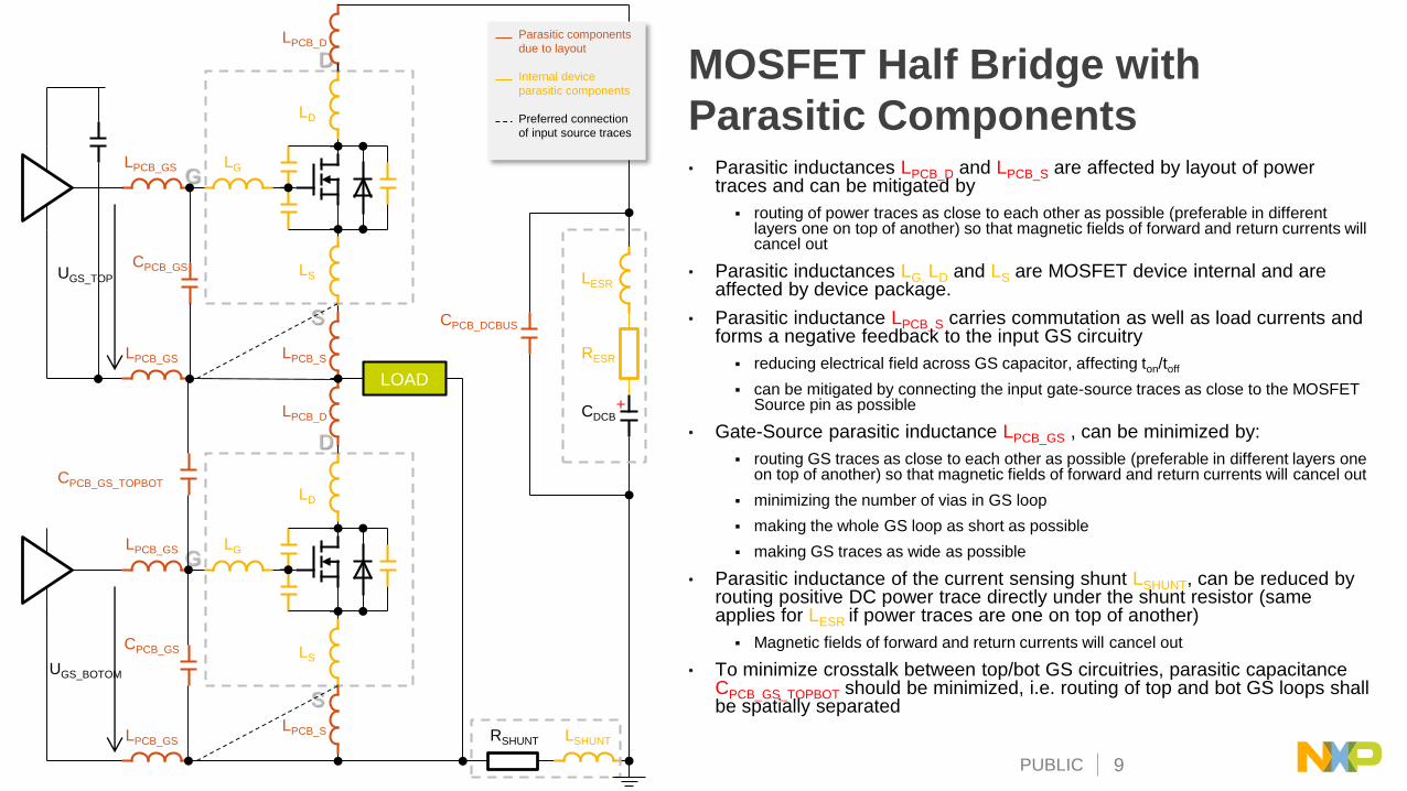
MOSFET Half Bridge with
Parasitic Components• Parasitic inductances LPCB_D and LPCB_S are affected by layout of power
traces and can be mitigated by
routing of power traces as close to each other as possible (preferable in different layers one on top of another) so that magnetic fields of forward and return currents will cancel out
• Parasitic inductances LG, LD and LS are MOSFET device internal and are affected by device package.
• Parasitic inductance LPCB_S carries commutation as well as load currents and forms a negative feedback to the input GS circuitry
reducing electrical field across GS capacitor, affecting ton/toff
can be mitigated by connecting the input gate-source traces as close to the MOSFET Source pin as possible
• Gate-Source parasitic inductance LPCB_GS , can be minimized by:
routing GS traces as close to each other as possible (preferable in different layers one on top of another) so that magnetic fields of forward and return currents will cancel out
minimizing the number of vias in GS loop
making the whole GS loop as short as possible
making GS traces as wide as possible
• Parasitic inductance of the current sensing shunt LSHUNT, can be reduced by routing positive DC power trace directly under the shunt resistor (same applies for LESR if power traces are one on top of another)
Magnetic fields of forward and return currents will cancel out
• To minimize crosstalk between top/bot GS circuitries, parasitic capacitance CPCB_GS_TOPBOT should be minimized, i.e. routing of top and bot GS loops shall be spatially separated
LOAD
+
D
S
G
LS
LD
LG
LPCB_S
D
S
G
LS
LD
LG
LPCB_D
LPCB_S
LPCB_GS
CPCB_GS
LPCB_D
LESR
RESR
CDCB
RSHUNT LSHUNT
UGS_BOTOM
UGS_TOP
LPCB_GS
LPCB_GS
Parasitic components
due to layout
Internal device
parasitic components
Preferred connection
of input source traces
LPCB_GS
CPCB_GS
CPCB_DCBUS
CPCB_GS_TOPBOT
PUBLIC 10
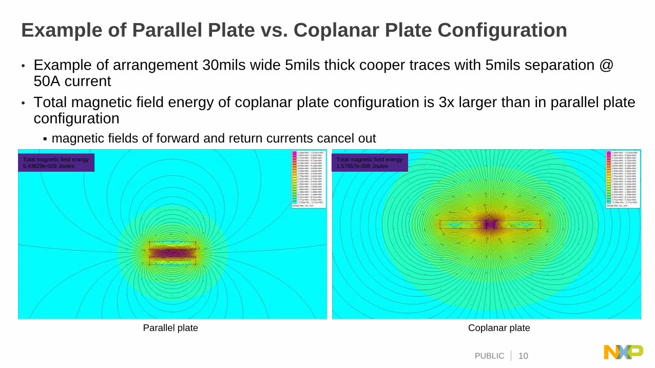
Example of Parallel Plate vs. Coplanar Plate Configuration
• Example of arrangement 30mils wide 5mils thick cooper traces with 5mils separation @ 50A current
• Total magnetic field energy of coplanar plate configuration is 3x larger than in parallel plate configuration
magnetic fields of forward and return currents cancel out
Total magnetic field energy
5.43829e-009 Joules
Total magnetic field energy
1.57957e-008 Joules
Parallel plate Coplanar plate
PUBLIC 11
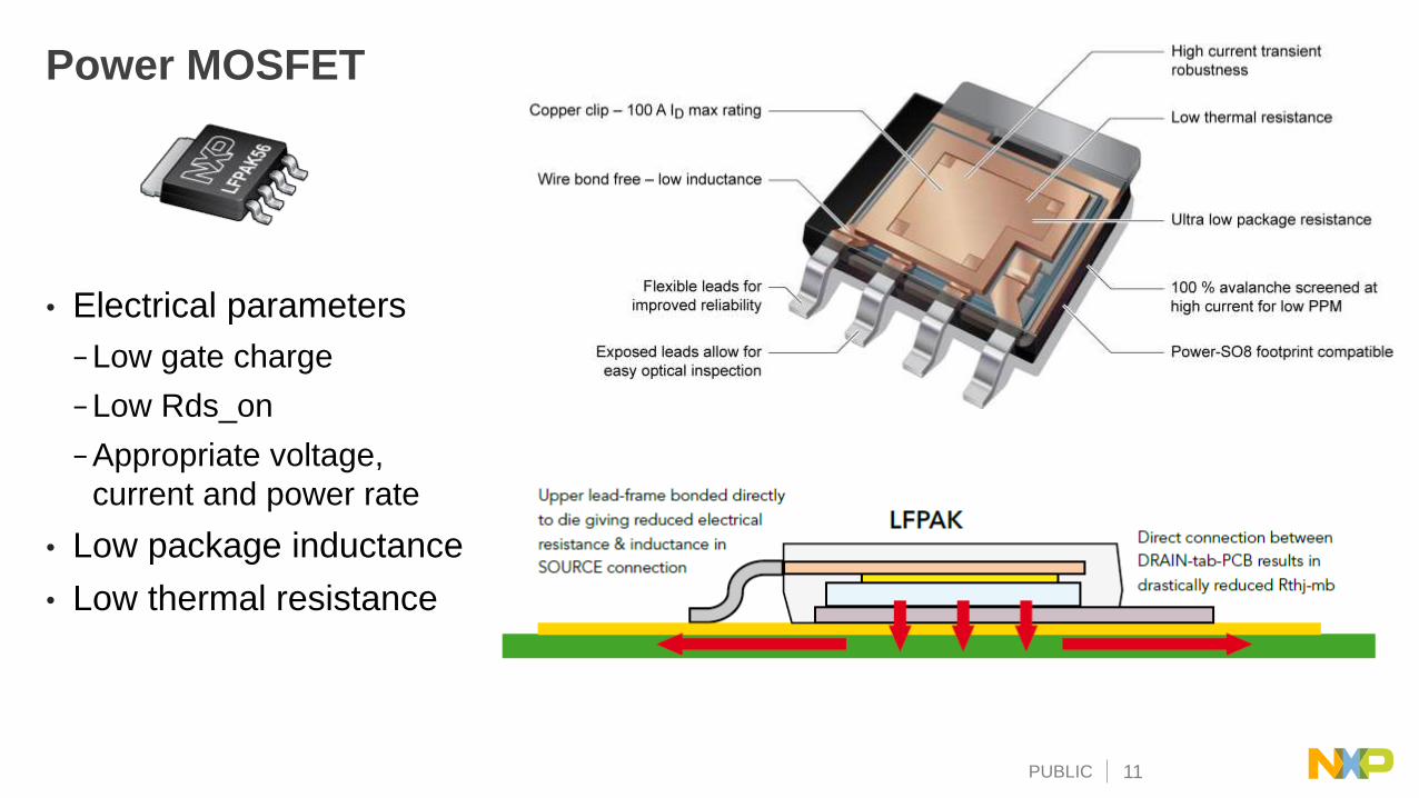
Power MOSFET
• Electrical parameters
−Low gate charge
−Low Rds_on
−Appropriate voltage,
current and power rate
• Low package inductance
• Low thermal resistance
PUBLIC 12
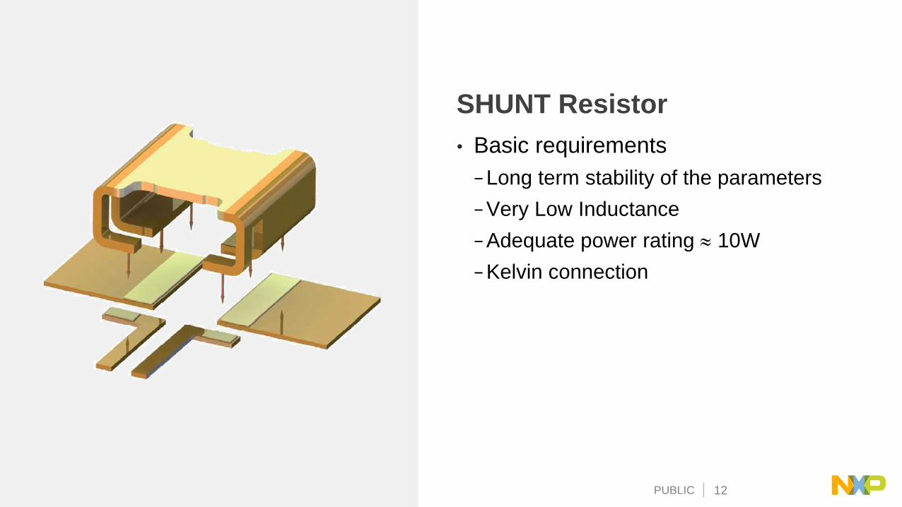
SHUNT Resistor
• Basic requirements
−Long term stability of the parameters
−Very Low Inductance
−Adequate power rating 10W
−Kelvin connection
PUBLIC 13
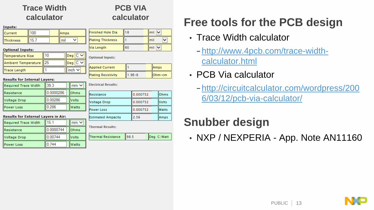
Free tools for the PCB design
• Trace Width calculator
−http://www.4pcb.com/trace-width-
calculator.html
• PCB Via calculator
−http://circuitcalculator.com/wordpress/200
6/03/12/pcb-via-calculator/
Trace Width
calculator
PCB VIA
calculator
Snubber design
• NXP / NEXPERIA - App. Note AN11160

PUBLIC 14
NXP MC High Current Solution03.
PUBLIC 15
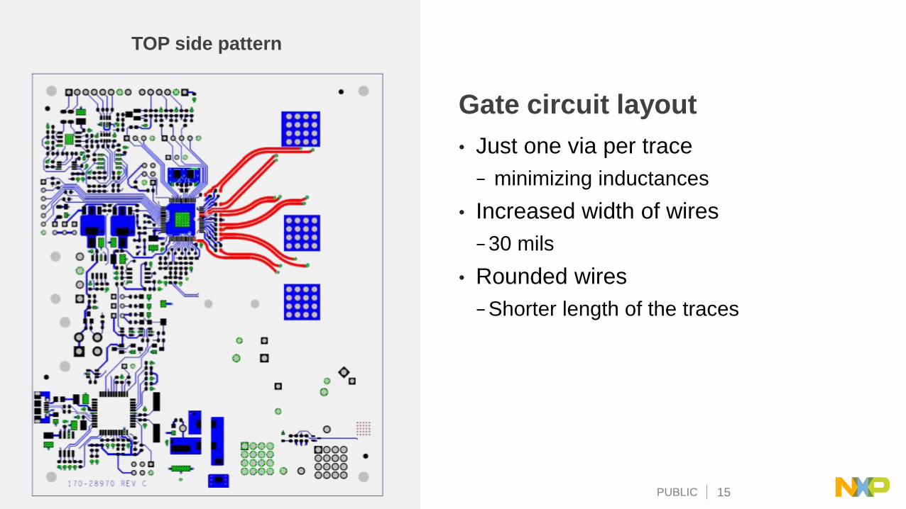
Gate circuit layout
• Just one via per trace
− minimizing inductances
• Increased width of wires
−30 mils
• Rounded wires
−Shorter length of the traces
TOP side pattern
PUBLIC 16
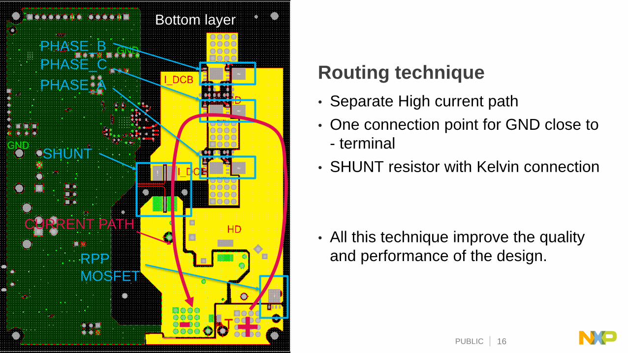
Routing technique
• Separate High current path
• One connection point for GND close to
- terminal
• SHUNT resistor with Kelvin connection
• All this technique improve the quality
and performance of the design.
Bottom layer
+-
PHASE_B
PHASE_C
PHASE_A
SHUNT
RPP
MOSFET
CURRENT PATH
PUBLIC 17
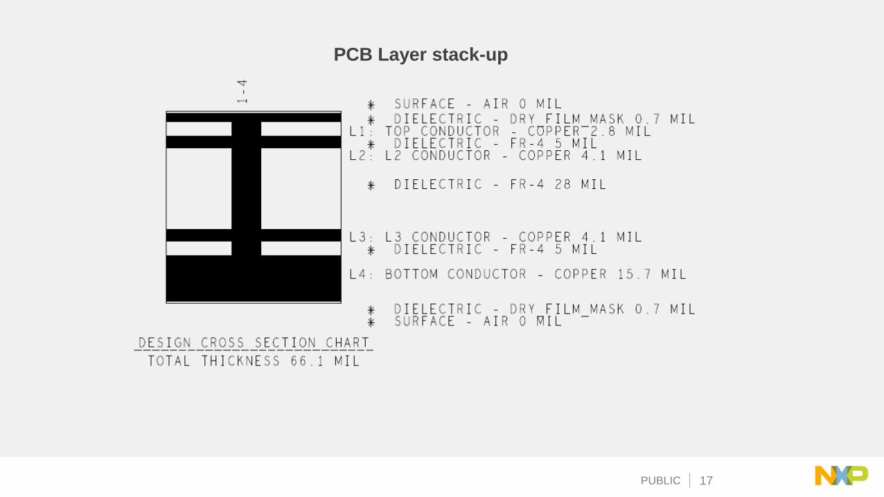
PCB Layer stack-up
PUBLIC 18
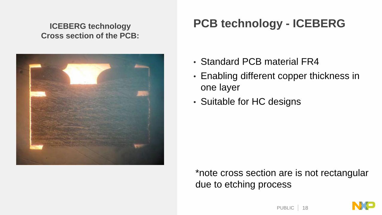
PCB technology - ICEBERG
• Standard PCB material FR4
• Enabling different copper thickness in
one layer
• Suitable for HC designs
*note cross section are is not rectangular
due to etching process
ICEBERG technology
Cross section of the PCB:

PUBLIC 19
HEATSINK
• Designed to fit PCB.
• Material - Aluminum
• Conductive thermal foil
• Four mounting points

PUBLIC 20
MAGNIV Dev. Board Performance04.
PUBLIC 21
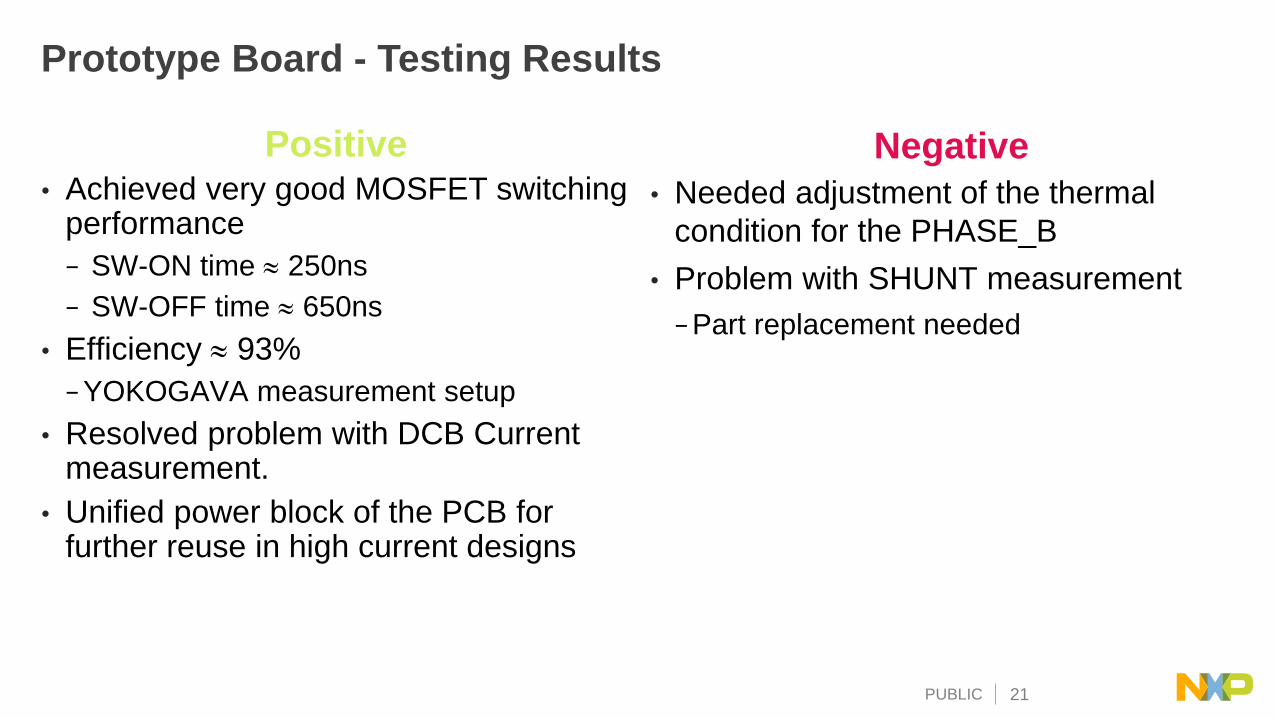
Prototype Board - Testing Results
• Achieved very good MOSFET switching performance
− SW-ON time 250ns
− SW-OFF time 650ns
• Efficiency 93%
−YOKOGAVA measurement setup
• Resolved problem with DCB Current measurement.
• Unified power block of the PCB for further reuse in high current designs
• Needed adjustment of the thermal
condition for the PHASE_B
• Problem with SHUNT measurement
−Part replacement needed
Positive Negative
PUBLIC 22
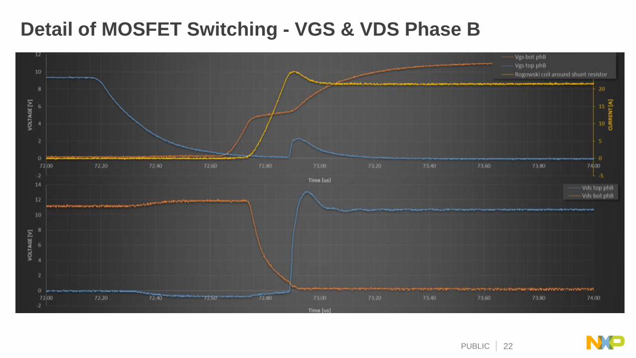
Detail of MOSFET Switching - VGS & VDS Phase B

PUBLIC 23
MAGNIV Development Board Features05.
PUBLIC 24
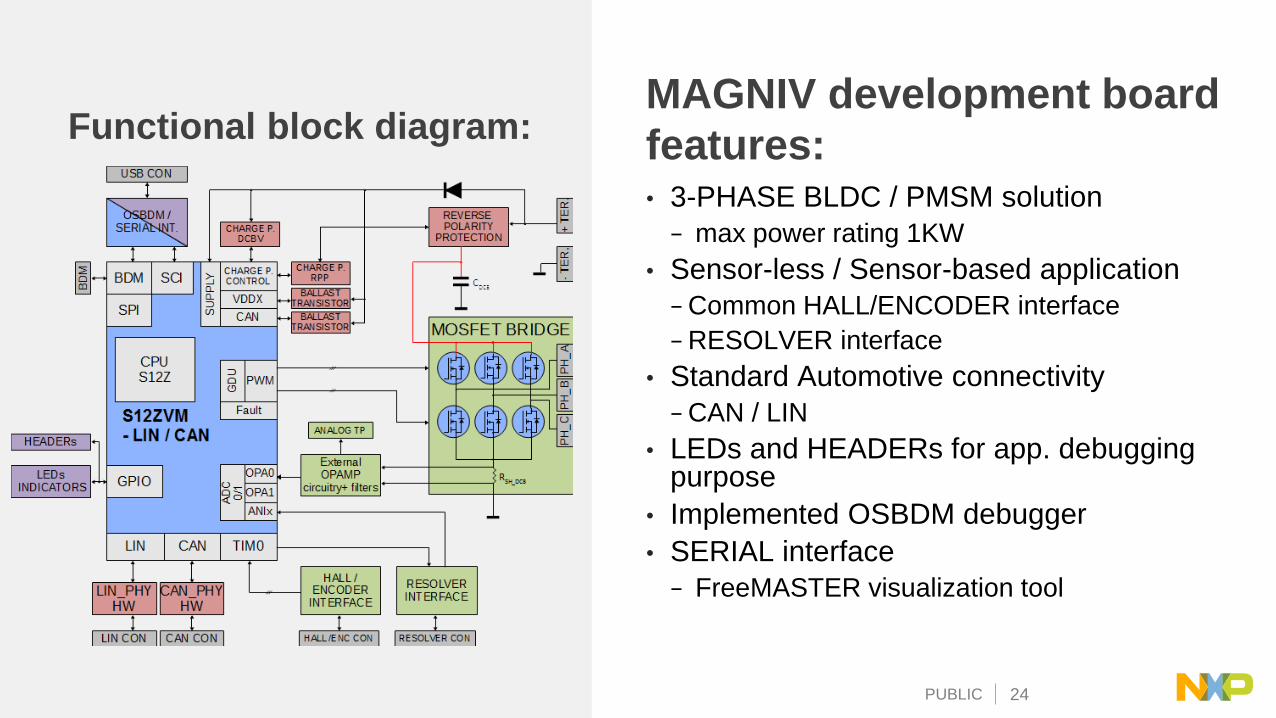
Functional block diagram:MAGNIV development board
features:• 3-PHASE BLDC / PMSM solution
− max power rating 1KW
• Sensor-less / Sensor-based application
− Common HALL/ENCODER interface
− RESOLVER interface
• Standard Automotive connectivity
− CAN / LIN
• LEDs and HEADERs for app. debugging purpose
• Implemented OSBDM debugger
• SERIAL interface
− FreeMASTER visualization tool
PUBLIC 25
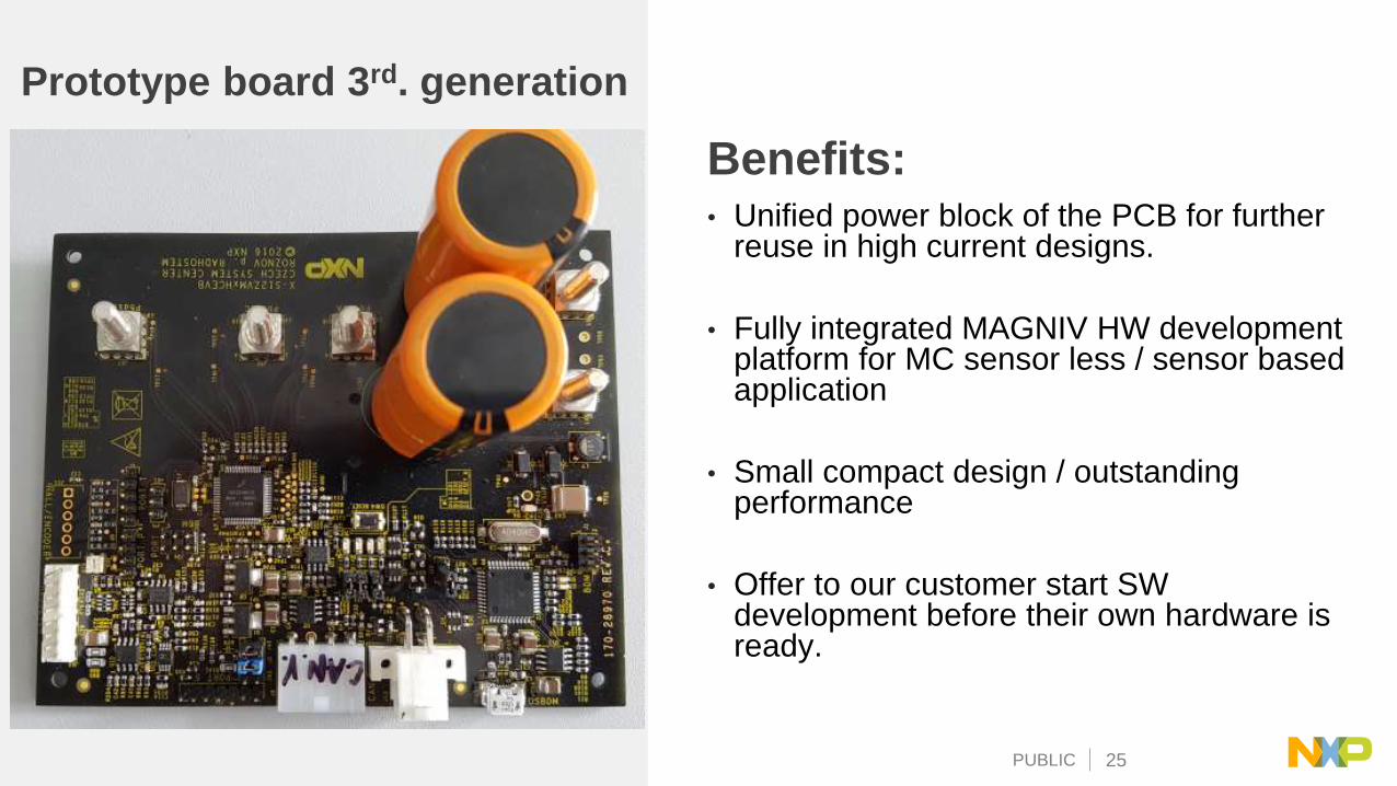
Prototype board 3rd. generation
Benefits:• Unified power block of the PCB for further
reuse in high current designs.
• Fully integrated MAGNIV HW development platform for MC sensor less / sensor based application
• Small compact design / outstanding performance
• Offer to our customer start SW development before their own hardware is ready.
PUBLIC 26
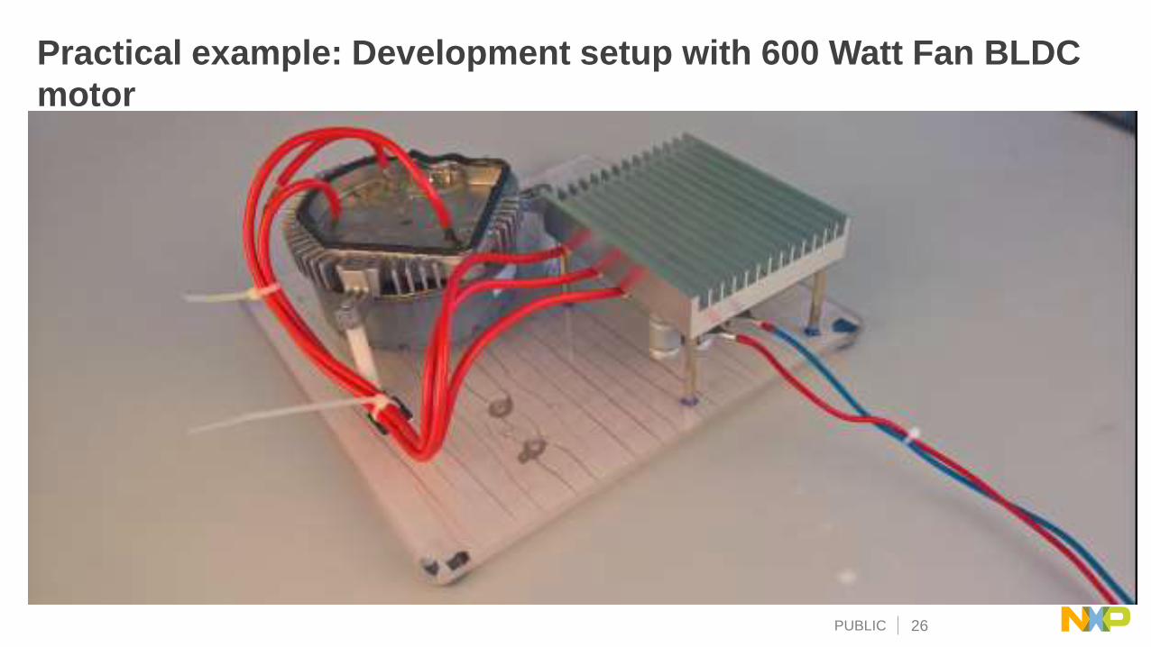
Practical example: Development setup with 600 Watt Fan BLDC
motor
PUBLIC 27
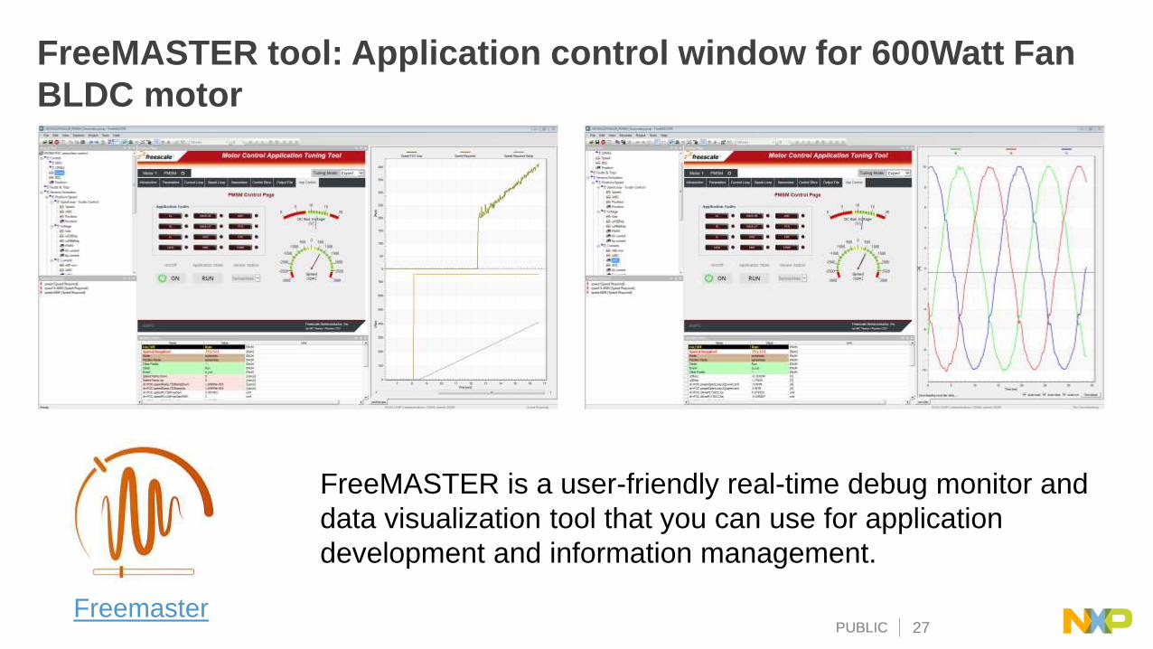
FreeMASTER tool: Application control window for 600Watt Fan
BLDC motor
Freemaster
FreeMASTER is a user-friendly real-time debug monitor and
data visualization tool that you can use for application
development and information management.

PUBLIC 28
2017 Outlook 06.
PUBLIC 29
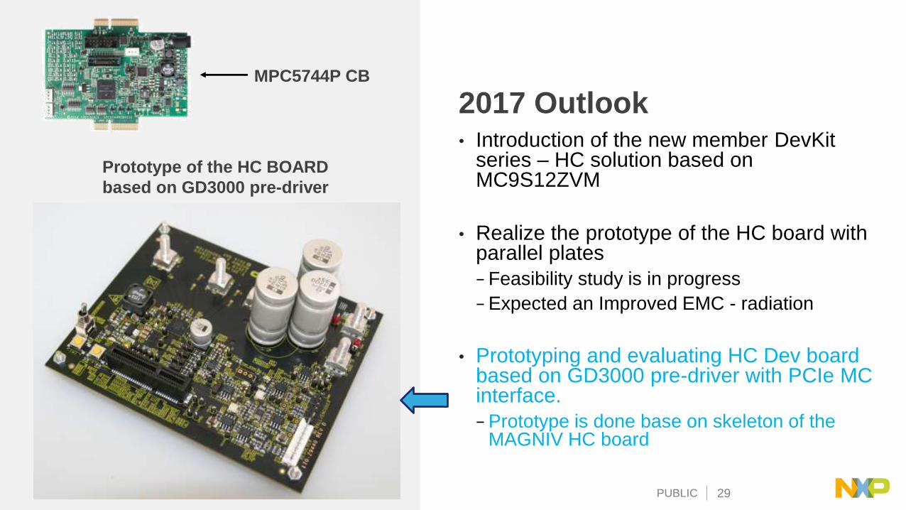
Prototype of the HC BOARD
based on GD3000 pre-driver
MPC5744P CB
2017 Outlook• Introduction of the new member DevKit
series – HC solution based on MC9S12ZVM
• Realize the prototype of the HC board with parallel plates
− Feasibility study is in progress
− Expected an Improved EMC - radiation
• Prototyping and evaluating HC Dev board based on GD3000 pre-driver with PCIe MC interface.
− Prototype is done base on skeleton of the MAGNIV HC board

PUBLIC 30
Conclusion07.
PUBLIC 31
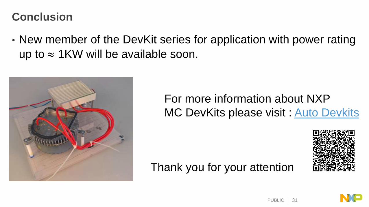
Conclusion
• New member of the DevKit series for application with power rating
up to 1KW will be available soon.
For more information about NXP
MC DevKits please visit : Auto Devkits
Thank you for your attention

NXP and the NXP logo are trademarks of NXP B.V. All other product or service names are the property of their respective owners. © 2017 NXP B.V.
Recommended
![[PPT]Direct – Current Motor Characteristics and … · Web viewDirect – Current Motor Characteristics and Applications Straight Shunt Motor Essentially a constant speed motor](https://img.pdfslide.us/doc/110x75/5add0e687f8b9a4a268d0073/pptdirect-current-motor-characteristics-and-viewdirect-current-motor.jpg)