M. Lozano, C. Fleta*, G. Pellegrini, M. Ullán, F. Campabadal, J. M. Rafí
CNM-IMB (CSIC), Barcelona, Spain(*) Currently at University of Glasgow, UK
S. Martí, C. García, C. Lacasta, M. Miñano
IFIC (CSIC), Valencia, Spain
Prague, 26th June 2006
IMB-CNM and IFICactivities in P-type detectors
IMB-CNM and IFICactivities in P-type detectors

2006 RD50 Meeting, Prague 2
IMB-CNM Barcelona, IFIC Valencia (CSIC)
Index Our first intention was to report only the "Development of
Moderated p-spray Isolation Techniques for P-type Detectors at CNM"
Unfortunately, the clean room process is not yet finished We will explain the activities of CNM and IFIC in P-type
detectors
TOPICSI. Finishing of RD50 processingII. Simulation and processing of moderated p-spray isolation techniquesIII. First module with 3 cm p-type strip detectors
2006 RD50 Meeting, Prague 3
IMB-CNM Barcelona, IFIC Valencia (CSIC)
I. Finishing of RD50 processing

2006 RD50 Meeting, Prague 4
IMB-CNM Barcelona, IFIC Valencia (CSIC)
RD50 process The p-spray technology is ready We have found a set of implant conditions that offer enough
strip insulation, keeping the breakdown voltage high enough Energy, E=100 keV, dose = 31012 cm-2
We checked with gamma irradiation that the insulation is kept after oxide charge saturation
A set of 22 wafers has been processed using RD50 microstrip mask set with the above implant conditions
Wafers are diced and will be stored at CERN for irradiation and/or collection

2006 RD50 Meeting, Prague 5
IMB-CNM Barcelona, IFIC Valencia (CSIC)
Reminder of RD50 processTechnology Wafers
Growing method
TypeWafer origin
Comments
P-in-N4 MCZ N RD50 >500 ·cm, 300 µm
2 EPI N RD50 thickness ~ 150 µm
N-in-P
4 (+1) MCZ P RD50 >2 k·cm, 300 µm
4 FZ P CNM
4 (+1) FZ P CNM Oxygen enriched DOFZ
2 EPI P RD50 thickness ~ 150 µm
N-in-N 2 FZ N CNM Single side processing
TOTAL 22 (+2)

2006 RD50 Meeting, Prague 6
IMB-CNM Barcelona, IFIC Valencia (CSIC)
Reminder of RD50 microstrip mask set
Technology• P-in-N and N-in-P
Mask set• Designed by the RD50
Collaboration• Double-side processing• One metal layer
Structures• 26 microstrip detectors
- Polysilicon biasing resistors- Capacitive coupling- P-spray insulation- No p-stops
• 20 pad detectors• 12 pixel detectors• 8 test structure sets

2006 RD50 Meeting, Prague 7
IMB-CNM Barcelona, IFIC Valencia (CSIC)
Results IV plots of un-diced wafers
detector: solid line ring: dashed line Absolute current at 20ºC plotted Diode area = 1 cm2 aprox.
Good performance for most of the wafers
Irreversible breakdown in some wafers n-in-n & n-in-p. Oxide damage Always in guard ring VBD well above VFD, no problem for use, but care must be taken

2006 RD50 Meeting, Prague 8
IMB-CNM Barcelona, IFIC Valencia (CSIC)
N-in-P DOFZ3297-NP-DOFZ
300um, SILHRP(9/05) OXG
1.E-09
1.E-08
1.E-07
1.E-06
1.E-05
0 50 100 150 200 250 300 350 400
Vrev (V)
I@20
º (A
)
Wafer 5
Wafer 5
Wafer 6
Wafer 7Wafer 8
Wafer 9

2006 RD50 Meeting, Prague 9
IMB-CNM Barcelona, IFIC Valencia (CSIC)
N-in-P MCZ3297-NP-MCZ
300um, >2kohm.cmSENMCZP (4/04)
1.E-09
1.E-08
1.E-07
1.E-06
1.E-05
1.E-04
1.E-03
1.E-02
0 50 100 150 200 250 300 350 400
Vrev (V)
I@20
º (A
)
Wafer 10
Wafer 11Wafer 12
Wafer 13
Wafer 14
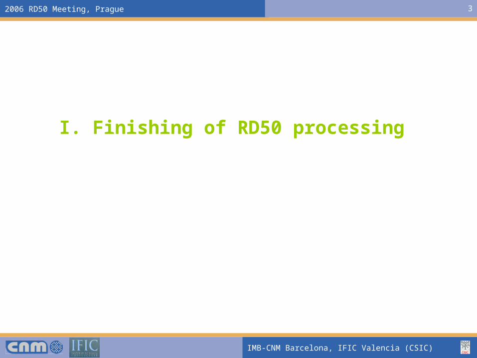
2006 RD50 Meeting, Prague 10
IMB-CNM Barcelona, IFIC Valencia (CSIC)
N-in-P EPI
3297-NP-EPI150um
1.E-09
1.E-08
1.E-07
1.E-06
1.E-05
1.E-04
1.E-03
0 50 100 150 200 250 300
Vrev (V)
I@20
º (A
)
Wafer 15
Wafer 16

2006 RD50 Meeting, Prague 11
IMB-CNM Barcelona, IFIC Valencia (CSIC)
N-in-P FZ
3297-NP-FZ300 um
SILHRP(9/05)1.E-10
1.E-09
1.E-08
1.E-07
1.E-06
0 50 100 150 200 250 300 350 400 450 500
Vrev (V)
I@20
º (A
)
Wafer 1-FZWafer 4-FZ
ruptura irreversible del anillo de guarda
Irreversiblebreakdown in guard ring

2006 RD50 Meeting, Prague 12
IMB-CNM Barcelona, IFIC Valencia (CSIC)
N-in-N FZ3297-NN280 um
SILHRN2C(9/05)
1.E-09
1.E-08
1.E-07
1.E-06
1.E-05
1.E-04
1.E-03
0 50 100 150 200 250 300 350 400
Vrev (V)
I@20
º (A
)
Wafer 17-FZ
Wafer 17-FZ
Wafer 18-FZ
ruptura irreversible de los anillos de guarda
Irreversiblebreakdown in guard ring

2006 RD50 Meeting, Prague 13
IMB-CNM Barcelona, IFIC Valencia (CSIC)
P-in-N MCZ3297-PN-MCZ
300 um, > 500 ohm.cm
1.E-09
1.E-08
1.E-07
1.E-06
0 100 200 300 400 500 600 700
Vrev (V)
I@20
º (A
)
Wafer 19
Wafer 20Wafer 21
Wafer 22

2006 RD50 Meeting, Prague 14
IMB-CNM Barcelona, IFIC Valencia (CSIC)
P-in-N EPI3297-PN-EPI
150 um
1.E-09
1.E-08
1.E-07
1.E-06
0 50 100 150 200 250 300
Vrev (V)
I@20
º (A
)
Wafer 23
Wafer 24

2006 RD50 Meeting, Prague 15
IMB-CNM Barcelona, IFIC Valencia (CSIC)
N-in-P FZ CV curve
0.00E+00
1.00E+20
2.00E+20
3.00E+20
4.00E+20
5.00E+20
6.00E+20
7.00E+20
0 20 40 60 80 100 120 140 160 180 200
VFD = 35 V

2006 RD50 Meeting, Prague 16
IMB-CNM Barcelona, IFIC Valencia (CSIC)
Some comments Similar current levels for all substrates (10-7 A/cm2) Same for ring current in (almost all) p-n and n-p (10-8 A) That means that n-in-p are so well insulated that they
behave like p-in-n Wafers 13 and 14 (p-MCZ) and 15 and 16 (p-EPI) behave as
if they do not have p-spray. Ring current very high, diode current normal Not due to substrate type Consecutive wafers: problem with ion implanter? Dicing and irradiation will improve problem
N-in-n as expected No backside implant

2006 RD50 Meeting, Prague 17
IMB-CNM Barcelona, IFIC Valencia (CSIC)
II. Simulation and processing of moderated p-spray isolation techniques

2006 RD50 Meeting, Prague 18
IMB-CNM Barcelona, IFIC Valencia (CSIC)
Moderated p-spray As already presented in February in Trento We have developed through simulation a technology for p-
type detectors with moderated p-spray insulation Boron implant parameters are selected from our previous
experience with microstrip with p-stops: 50 keV, 1013 cm-2, implant oxide thickness
With less p-spray implanted charge, we obtain: High VBD, Good insulation, Eliminate the high field corner in the p-stop causing
microdischarges

2006 RD50 Meeting, Prague 19
IMB-CNM Barcelona, IFIC Valencia (CSIC)
Doping profile comparison
X
Y
20 30 40
-2
0
2
4
6
AcceptorConcentration2.2E+19
2.9E+09
4.0E-01
5.4E-11
7.4E-21
1.0E-30
diode_np_mdr.grd - n1_des_moderatedpspray400min_10um_Qox1e11_h1X
Y
20 30 40
-5
0
5
10
AcceptorConcentration2.2E+19
2.9E+09
4.0E-01
5.4E-11
7.4E-21
1.0E-30
diode_np_mdr.grd - n1_des_solopstop_10um_Qox1e11_h1000V.dat
P-stop only
Moderatedp-spray
N strip P-stop
P-spray

2006 RD50 Meeting, Prague 20
IMB-CNM Barcelona, IFIC Valencia (CSIC)
Electric field comparison
X
Y
20 30 40
-2
0
2
4
6
ElectricField3.2E+05
2.5E+05
1.9E+05
1.3E+05
6.3E+04
0.0E+00
diode_np_mdr.grd - n1_des_moderatedpspray340min_10um_Qox1e11_h1
X
Y
20 30 40
-5
0
5
10
ElectricField3.2E+05
2.6E+05
1.9E+05
1.3E+05
6.4E+04
0.0E+00
diode_np_mdr.grd - n1_des_solopstop_10um_Qox1e11_h1000V.dat
P-stop only
Moderatedp-spray
microdischarges?N strip P-stop
P-spray

2006 RD50 Meeting, Prague 21
IMB-CNM Barcelona, IFIC Valencia (CSIC)
Technology First: oxidation, photolitograpy p-stop regions, wet oxide
etching, re-oxidation, photoresist striping At this point there are two different oxide thicknesses
thin oxide in the p-stop area and a thicker oxide on the rest of the silicon surface (“p-spray area”)
P-implant (Energy 50 keV, dose 1013 cm-2) Finish with the usual fabrication process
First fabrication batch with mask set CNM275 pad detectors process with dummy poly deposition to have the same
thermal budget as in microstrips Finished in one week MCZ and FZ silicon with p-stop, p-spray and moderate p-spray.

2006 RD50 Meeting, Prague 22
IMB-CNM Barcelona, IFIC Valencia (CSIC)
CNM275 mask set New mask set to replace
old ROSE set 100 pad diodes with
improved guard ring Diodes are labelled from
00 to 99. Only one type of diodes Designed for simplicity
and fast dicing Other test structures
2006 RD50 Meeting, Prague 23
IMB-CNM Barcelona, IFIC Valencia (CSIC)
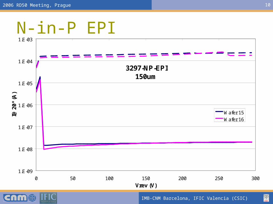
New mask design One additional layer
needed from RD50 microstrip mask set – is being laid out.
Common p-stops p-spray increases safety
Distance between n-strip and p-stop is maximized To achieve higher
breakdown voltages narrow p-stops
2006 RD50 Meeting, Prague 24
IMB-CNM Barcelona, IFIC Valencia (CSIC)
III. First modules with 3 cm p-type strip detectors

2006 RD50 Meeting, Prague 25
IMB-CNM Barcelona, IFIC Valencia (CSIC)
ATLAS SCTDAC readout for p-type sensors Aim: to read a 3 cm p-type detector using the ATLAS
SCTDAC readout. SCTDAC is optimised for n-type sensor. SCT readout: binary ABCD3T chip. We have assembled at IFIC-Valencia a “pseudo SCT
module” with a 3cm p-type sensor and a 3 cm n-type sensor (from CNM-Barcelona) to crosscheck, using all the assembly tools of the SCT end-cap module: assembly jigs, bonding jigs, fan-in adaptors, test box and frames, etc..
2006 RD50 Meeting, Prague 26
IMB-CNM Barcelona, IFIC Valencia (CSIC)
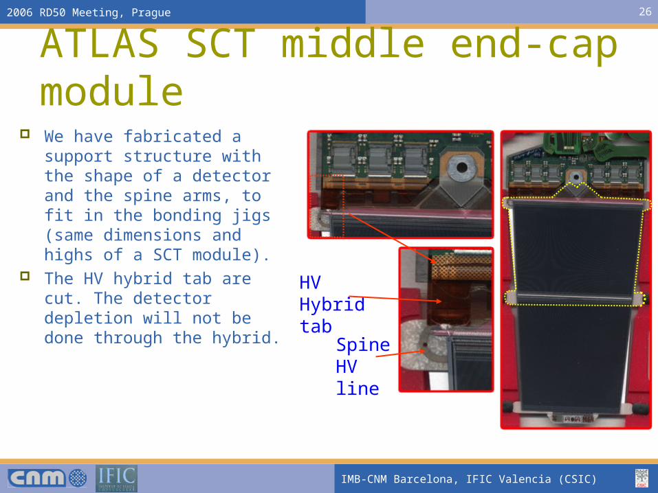
ATLAS SCT middle end-cap module
We have fabricated a support structure with the shape of a detector and the spine arms, to fit in the bonding jigs (same dimensions and highs of a SCT module).
The HV hybrid tab are cut. The detector depletion will not be done through the hybrid.
HV Hybrid tab
Spine HV line

2006 RD50 Meeting, Prague 27
IMB-CNM Barcelona, IFIC Valencia (CSIC)
Support structureThe support structure has been manufactured using a circuit board, the 3cm detector will be hold in the cupper rectangles.
The height of the support structure fits in the assembling and bonding jigs
The structure fits in the transport frame

2006 RD50 Meeting, Prague 28
IMB-CNM Barcelona, IFIC Valencia (CSIC)
Hybrid assembling Gluing of the hybrid in the
SCT assembly jig. The HV tab has been cut
2006 RD50 Meeting, Prague 29
IMB-CNM Barcelona, IFIC Valencia (CSIC)
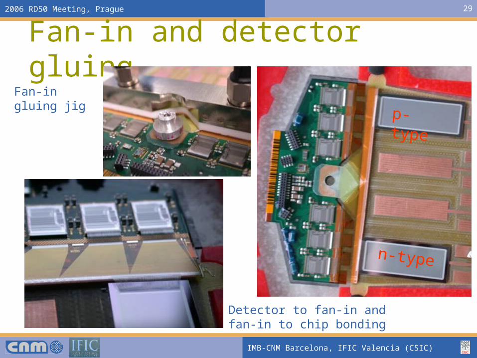
Fan-in and detector gluingFan-in gluing jig
Detector to fan-in and fan-in to chip bonding
n-type
p-type

2006 RD50 Meeting, Prague 30
IMB-CNM Barcelona, IFIC Valencia (CSIC)
p-type
n-type
Module in the test box
Cooling injecting cold air
Strips to ground HV to the back plane
The detectors are not read simultaneously.
Detector biasing:
+HV for n-type
HV for p-type

2006 RD50 Meeting, Prague 31
IMB-CNM Barcelona, IFIC Valencia (CSIC)
Work in progress: Modifying SCTDAC to read
negative pulses for p-type sensors.
Laser and source setups ready to do a full study.
Still place in this module for two more sensors.
Irradiated sensor available to be assembled at 1015
n/cm2 .
IFIC-Valencia automatic laser system with 3 staged and automatic focusing in 20 min.
Recommended