TL/H/12439
LM
2594
SIM
PLE
SW
ITC
HER
Pow
erC
onverte
r150
kH
z0.5
ASte
p-D
ow
nV
olta
ge
Regula
tor
July 1995
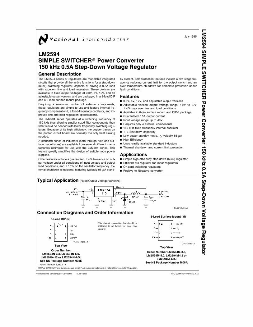
LM2594SIMPLE SWITCHERÉ Power Converter150 kHz 0.5A Step-Down Voltage RegulatorGeneral DescriptionThe LM2594 series of regulators are monolithic integrated
circuits that provide all the active functions for a step-down
(buck) switching regulator, capable of driving a 0.5A load
with excellent line and load regulation. These devices are
available in fixed output voltages of 3.3V, 5V, 12V, and an
adjustable output version, and are packaged in a 8-lead DIP
and a 8-lead surface mount package.
Requiring a minimum number of external components,
these regulators are simple to use and feature internal fre-
quency compensation², a fixed-frequency oscillator, and im-
proved line and load regulation specifications.
The LM2594 series operates at a switching frequency of
150 kHz thus allowing smaller sized filter components than
what would be needed with lower frequency switching regu-
lators. Because of its high efficiency, the copper traces on
the printed circuit board are normally the only heat sinking
needed.
A standard series of inductors (both through hole and sur-
face mount types) are available from several different manu-
facturers optimized for use with the LM2594 series. This
feature greatly simplifies the design of switch-mode power
supplies.
Other features include a guaranteed g4% tolerance on out-
put voltage under all conditions of input voltage and output
load conditions, and g15% on the oscillator frequency. Ex-
ternal shutdown is included, featuring typically 85 mA stand-
by current. Self protection features include a two stage fre-
quency reducing current limit for the output switch and an
over temperature shutdown for complete protection under
fault conditions.
FeaturesY 3.3V, 5V, 12V, and adjustable output versionsY Adjustable version output voltage range, 1.2V to 37V
g4% max over line and load conditionsY Available in 8-pin surface mount and DIP-8 packageY Guaranteed 0.5A output currentY Input voltage range up to 40VY Requires only 4 external componentsY 150 kHz fixed frequency internal oscillatorY TTL Shutdown capabilityY Low power standby mode, IQ typically 85 mAY High EfficiencyY Uses readily available standard inductorsY Thermal shutdown and current limit protection
ApplicationsY Simple high-efficiency step-down (buck) regulatorY Efficient pre-regulator for linear regulatorsY On-card switching regulatorsY Positive to Negative convertor
Typical Application (Fixed Output Voltage Versions)
TL/H/12439–1
Connection Diagrams and Order Information
8-Lead DIP (N)
TL/H/12439–2
Top View
Order Number
LM2594N-3.3, LM2594N-5.0,
LM2594N-12 or LM2594N-ADJ
See NS Package Number N08E
*No internal connection, but should be
soldered to pc board for best heat
transfer.
8-Lead Surface Mount (M)
TL/H/12439–3
Top View
Order Number LM2594M-3.3,
LM2594M-5.0, LM2594M-12 or
LM2594M-ADJ
See NS Package Number M08A²Patent Number 5,382,918.
SIMPLE SWITCHERÉ and Switchers Made SimpleÉ are registered trademarks of National Semiconductor Corporation.
C1995 National Semiconductor Corporation RRD-B30M115/Printed in U. S. A.
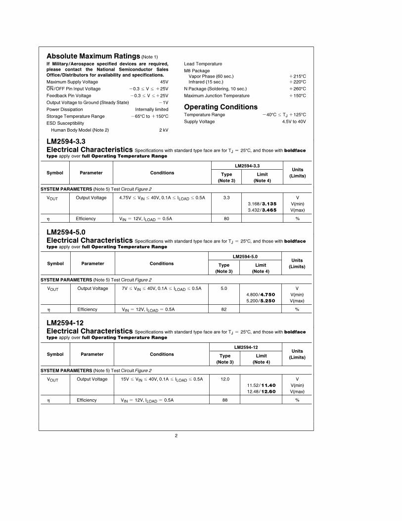
Absolute Maximum Ratings (Note 1)
If Military/Aerospace specified devices are required,
please contact the National Semiconductor Sales
Office/Distributors for availability and specifications.
Maximum Supply Voltage 45V
ON/OFF Pin Input Voltage b0.3 s V s a25V
Feedback Pin Voltage b0.3 s V sa25V
Output Voltage to Ground (Steady State) b1V
Power Dissipation Internally limited
Storage Temperature Range b65§C to a150§CESD Susceptibility
Human Body Model (Note 2) 2 kV
Lead Temperature
M8 Package
Vapor Phase (60 sec.) a215§CInfrared (15 sec.) a220§C
N Package (Soldering, 10 sec.) a260§CMaximum Junction Temperature a150§C
Operating ConditionsTemperature Range b40§C s TJ a125§CSupply Voltage 4.5V to 40V
LM2594-3.3Electrical Characteristics Specifications with standard type face are for TJ e 25§C, and those with boldfacetype apply over full Operating Temperature Range
Symbol Parameter Conditions
LM2594-3.3
(Limits)
UnitsType Limit
(Note 3) (Note 4)
SYSTEM PARAMETERS (Note 5) Test CircuitFigure 2
VOUT Output Voltage 4.75V s VIN s 40V, 0.1A s ILOAD s 0.5A 3.3 V
3.168/3.135 V(min)
3.432/3.465 V(max)
h Efficiency VIN e 12V, ILOAD e 0.5A 80 %
LM2594-5.0Electrical Characteristics Specifications with standard type face are for TJ e 25§C, and those with boldfacetype apply over full Operating Temperature Range
Symbol Parameter Conditions
LM2594-5.0
(Limits)
UnitsType Limit
(Note 3) (Note 4)
SYSTEM PARAMETERS (Note 5) Test CircuitFigure 2
VOUT Output Voltage 7V s VIN s 40V, 0.1A s ILOAD s 0.5A 5.0 V
4.800/4.750 V(min)
5.200/5.250 V(max)
h Efficiency VIN e 12V, ILOAD e 0.5A 82 %
LM2594-12Electrical Characteristics Specifications with standard type face are for TJ e 25§C, and those with boldfacetype apply over full Operating Temperature Range
Symbol Parameter Conditions
LM2594-12
(Limits)
UnitsType Limit
(Note 3) (Note 4)
SYSTEM PARAMETERS (Note 5) Test CircuitFigure 2
VOUT Output Voltage 15V s VIN s 40V, 0.1A s ILOAD s 0.5A 12.0 V
11.52/11.40 V(min)
12.48/12.60 V(max)
h Efficiency VIN e 12V, ILOAD e 0.5A 88 %
2
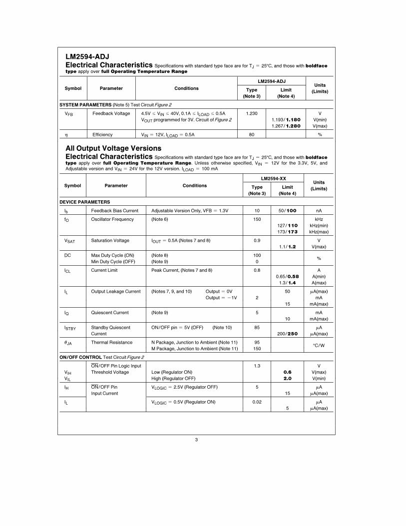
LM2594-ADJElectrical Characteristics Specifications with standard type face are for TJ e 25§C, and those with boldfacetype apply over full Operating Temperature Range
Symbol Parameter Conditions
LM2594-ADJ
(Limits)
UnitsType Limit
(Note 3) (Note 4)
SYSTEM PARAMETERS (Note 5) Test CircuitFigure 2
VFB Feedback Voltage 4.5V s VIN s 40V, 0.1A s ILOAD s 0.5A 1.230 V
VOUT programmed for 3V. Circuit ofFigure 2 1.193/1.180 V(min)
1.267/1.280 V(max)
h Efficiency VIN e 12V, ILOAD e 0.5A 80 %
All Output Voltage VersionsElectrical Characteristics Specifications with standard type face are for TJ e 25§C, and those with boldfacetype apply over full Operating Temperature Range. Unless otherwise specified, VIN e 12V for the 3.3V, 5V, and
Adjustable version and VIN e 24V for the 12V version. ILOAD e 100 mA
Symbol Parameter Conditions
LM2594-XX
(Limits)
UnitsType Limit
(Note 3) (Note 4)
DEVICE PARAMETERS
Ib Feedback Bias Current Adjustable Version Only, VFB e 1.3V 10 50/100 nA
fO Oscillator Frequency (Note 6) 150 kHz
127/110 kHz(min)
173/173 kHz(max)
VSAT Saturation Voltage IOUT e 0.5A (Notes 7 and 8) 0.9 V
1.1/1.2 V(max)
DC Max Duty Cycle (ON) (Note 8) 100%
Min Duty Cycle (OFF) (Note 9) 0
ICL Current Limit Peak Current, (Notes 7 and 8) 0.8 A
0.65/0.58 A(min)
1.3/1.4 A(max)
IL Output Leakage Current (Notes 7, 9, and 10) Output e 0V 50 mA(max)
Output e b1V 2 mA
15 mA(max)
IQ Quiescent Current (Note 9) 5 mA
10 mA(max)
ISTBY Standby Quiescent ON/OFF pin e 5V (OFF) (Note 10) 85 mA
Current 200/250 mA(max)
iJA Thermal Resistance N Package, Junction to Ambient (Note 11) 95§C/W
M Package, Junction to Ambient (Note 11) 150
ON/OFF CONTROL Test CircuitFigure 2
ON/OFF Pin Logic Input 1.3 V
VIH Threshold Voltage Low (Regulator ON) 0.6 V(max)
VIL High (Regulator OFF) 2.0 V(min)
IH ON/OFF Pin VLOGIC e 2.5V (Regulator OFF) 5 mA
Input Current 15 mA(max)
IL VLOGIC e 0.5V (Regulator ON) 0.02 mA
5 mA(max)
3
Electrical Characteristics (Continued)
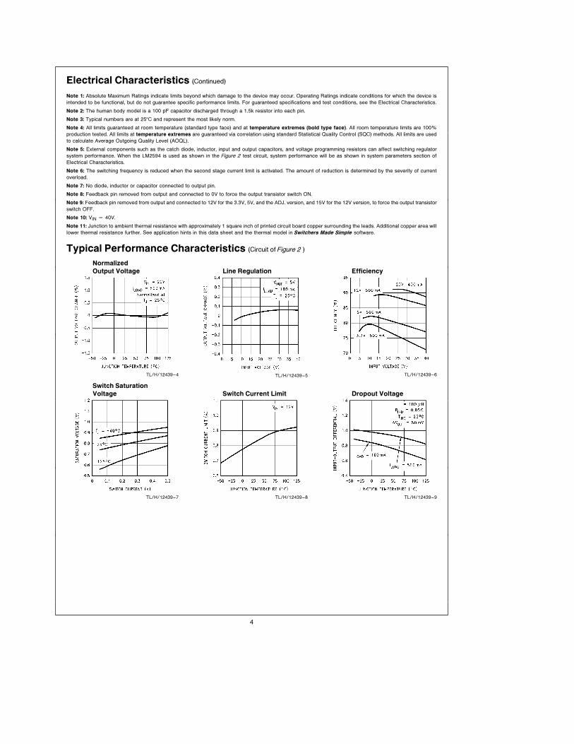
Note 1: Absolute Maximum Ratings indicate limits beyond which damage to the device may occur. Operating Ratings indicate conditions for which the device is
intended to be functional, but do not guarantee specific performance limits. For guaranteed specifications and test conditions, see the Electrical Characteristics.
Note 2: The human body model is a 100 pF capacitor discharged through a 1.5k resistor into each pin.
Note 3: Typical numbers are at 25§C and represent the most likely norm.
Note 4: All limits guaranteed at room temperature (standard type face) and at temperature extremes (bold type face). All room temperature limits are 100%
production tested. All limits at temperature extremes are guaranteed via correlation using standard Statistical Quality Control (SQC) methods. All limits are used
to calculate Average Outgoing Quality Level (AOQL).
Note 5: External components such as the catch diode, inductor, input and output capacitors, and voltage programming resistors can affect switching regulator
system performance. When the LM2594 is used as shown in the Figure 2 test circuit, system performance will be as shown in system parameters section of
Electrical Characteristics.
Note 6: The switching frequency is reduced when the second stage current limit is activated. The amount of reduction is determined by the severity of current
overload.
Note 7: No diode, inductor or capacitor connected to output pin.
Note 8: Feedback pin removed from output and connected to 0V to force the output transistor switch ON.
Note 9: Feedback pin removed from output and connected to 12V for the 3.3V, 5V, and the ADJ. version, and 15V for the 12V version, to force the output transistor
switch OFF.
Note 10: VIN e 40V.
Note 11: Junction to ambient thermal resistance with approximately 1 square inch of printed circuit board copper surrounding the leads. Additional copper area will
lower thermal resistance further. See application hints in this data sheet and the thermal model in Switchers Made Simple software.
Typical Performance Characteristics (Circuit ofFigure 2 )
Normalized
Output Voltage
TL/H/12439–4
Line Regulation
TL/H/12439–5
Efficiency
TL/H/12439–6
Switch Saturation
Voltage
TL/H/12439–7
Switch Current Limit
TL/H/12439–8
Dropout Voltage
TL/H/12439–9
4

Typical Performance Characteristics (Circuit ofFigure 2 ) (Continued)
Quiescent Current
TL/H/12439–10
Standby
Quiescent Current
TL/H/12439–11
Minimum Operating
Supply Voltage
TL/H/12439–12
ON/OFF Threshold
Voltage
TL/H/12439–13
ON/OFF Pin
Current (Sinking)
TL/H/12439–14
Switching Frequency
TL/H/12439–15
Feedback Pin
Bias Current
TL/H/12439–16
5

Typical Performance Characteristics (Circuit ofFigure 2 )
Continuous Mode Switching Waveforms
VIN e 20V, VOUT e 5V, ILOAD e 400 mA
L e 100 mH, COUT e 120 mF, COUT ESR e 140 mX
TL/H/12439–17
A: Output Pin Voltage, 10V/div.
B: Inductor Current 0.2A/div.
C: Output Ripple Voltage, 20 mV/div.
Horizontal Time Base: 2 ms/div.
Discontinuous Mode Switching Waveforms
VIN e 20V, VOUT e 5V, ILOAD e 200 mA
L e 33 mH, COUT e 220 mF, COUT ESR e 60 mX
TL/H/12439–18
A: Output Pin Voltage, 10V/div.
B: Inductor Current 0.2A/div.
C: Output Ripple Voltage, 20 mV/div.
Horizontal Time Base: 2 ms/div.
Load Transient Response for Continuous Mode
VIN e 20V, VOUT e 5V, ILOAD e 200 mA to 500 mA
L e 100 mH, COUT e 120 mF, COUT ESR e 140 mX
TL/H/12439–19
A: Output Voltage, 50 mV/div. (AC)
B: 200 mA to 500 mA Load Pulse
Horizontal Time Base: 50 ms/div.
Load Transient Response for Discontinuous Mode
VIN e 20V, VOUT e 5V, ILOAD e 100 mA to 200 mA
L e 33 mH, COUT e 220 mF, COUT ESR e 60 mX
TL/H/12439–20
A: Output Voltage, 50 mV/div. (AC)
B: 100 mA to 200 mA Load Pulse
Horizontal Time Base: 200 ms/div.
Block Diagram
TL/H/12439–21
FIGURE 1
6
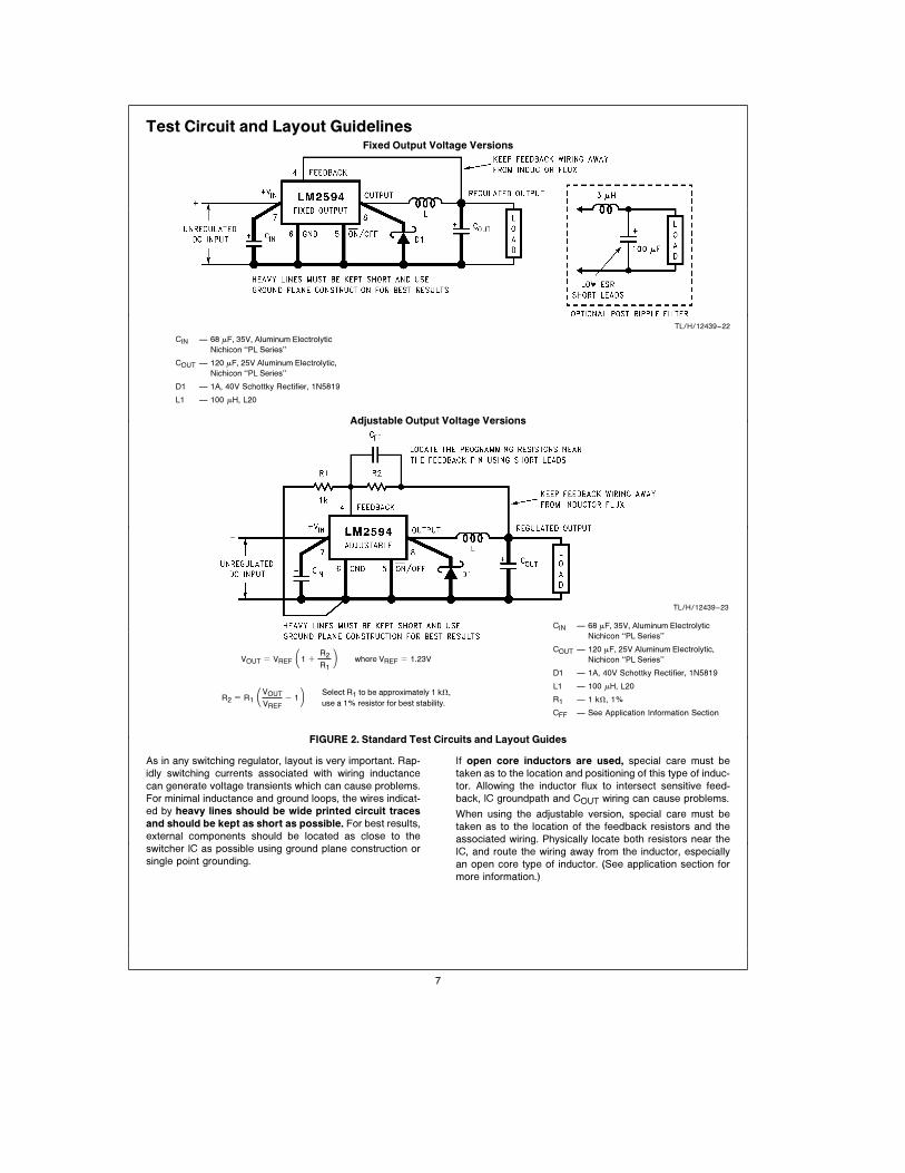
Test Circuit and Layout GuidelinesFixed Output Voltage Versions
TL/H/12439–22
CIN Ð 68 mF, 35V, Aluminum Electrolytic
Nichicon ‘‘PL Series’’
COUT Ð 120 mF, 25V Aluminum Electrolytic,
Nichicon ‘‘PL Series’’
D1 Ð 1A, 40V Schottky Rectifier, 1N5819
L1 Ð 100 mH, L20
Adjustable Output Voltage Versions
TL/H/12439–23
VOUT e VREF # 1 a
R2
R1 J where VREF e 1.23V
R2 e R1 #VOUT
VREF
b 1 J Select R1 to be approximately 1 kX,
use a 1% resistor for best stability.
CIN Ð 68 mF, 35V, Aluminum Electrolytic
Nichicon ‘‘PL Series’’
COUT Ð 120 mF, 25V Aluminum Electrolytic,
Nichicon ‘‘PL Series’’
D1 Ð 1A, 40V Schottky Rectifier, 1N5819
L1 Ð 100 mH, L20
R1 Ð 1 kX, 1%
CFF Ð See Application Information Section
FIGURE 2. Standard Test Circuits and Layout Guides
As in any switching regulator, layout is very important. Rap-
idly switching currents associated with wiring inductance
can generate voltage transients which can cause problems.
For minimal inductance and ground loops, the wires indicat-
ed by heavy lines should be wide printed circuit traces
and should be kept as short as possible. For best results,
external components should be located as close to the
switcher lC as possible using ground plane construction or
single point grounding.
If open core inductors are used, special care must be
taken as to the location and positioning of this type of induc-
tor. Allowing the inductor flux to intersect sensitive feed-
back, lC groundpath and COUT wiring can cause problems.
When using the adjustable version, special care must be
taken as to the location of the feedback resistors and the
associated wiring. Physically locate both resistors near the
IC, and route the wiring away from the inductor, especially
an open core type of inductor. (See application section for
more information.)
7
LM2594 Series Buck Regulator Design Procedure (Fixed Output)
PROCEDURE (Fixed Output Voltage Version) EXAMPLE (Fixed Output Voltage Version)
Given: Given:
VOUT e Regulated Output Voltage (3.3V, 5V or 12V) VOUT e 5V
VIN(max) e Maximum DC Input Voltage VIN(max) e 12V
ILOAD(max) e Maximum Load Current ILOAD(max) e 0.4A
1. Inductor Selection (L1) 1. Inductor Selection (L1)
A. Select the correct inductor value selection guide from A. Use the inductor selection guide for the 5V version
Figures 5, 6, or 7. (Output voltages of 3.3V, 5V, or 12V shown in Figure 6.respectively.) For all other voltages, see the design pro- B. From the inductor value selection guide shown in Fig-cedure for the adjustable version. ure 6, the inductance region intersected by the 12V hori-
B. From the inductor value selection guide, identify the zontal line and the 0.4A vertical line is 100 mH, and the
inductance region intersected by the Maximum Input inductor code is L20.
Voltage line and the Maximum Load Current line. Each C. The inductance value required is 100 mH. From theregion is identified by an inductance value and an induc- table inFigure 9, go to the L20 line and choose an induc-tor code (LXX). tor part number from any of the four manufacturers
C. Select an appropriate inductor from the four manufac- shown. (In most instance, both through hole and surface
turer’s part numbers listed in Figure 9. mount inductors are available.)
2. Output Capacitor Selection (COUT) 2. Output Capacitor Selection (COUT)
A. In the majority of applications, low ESR (Equivalent A. See section on output capacitors in application
Series Resistance) electrolytic capacitors between information section.
82 mF and 220 mF and low ESR solid tantalum capaci- B. From the quick design component selection tabletors between 15 mF and 100 mF provide the best results. shown in Figure 3, locate the 5V output voltage section.This capacitor should be located close to the IC using In the load current column, choose the load current lineshort capacitor leads and short copper traces. Do not that is closest to the current needed in your application,use capacitors larger than 220 mF. for this example, use the 0.5A line. In the maximum input
For additional information, see section on output ca- voltage column, select the line that covers the input volt-
pacitors in application information section. age needed in your application, in this example, use the
15V line. Continuing on this line are recommended in-B. To simplify the capacitor selection procedure, refer toductors and capacitors that will provide the best overallthe quick design component selection table shown inperformance.Figure 3. This table contains different input voltages, out-
put voltages, and load currents, and lists various induc- The capacitor list contains both through hole electrolytic
tors and output capacitors that will provide the best de- and surface mount tantalum capacitors from four differ-
sign solutions. ent capacitor manufacturers. It is recommended that
both the manufacturers and the manufacturer’s seriesC. The capacitor voltage rating for electrolytic capacitorsthat are listed in the table be used.should be at least 1.5 times greater than the output volt-
age, and often much higher voltage ratings are needed In this example aluminum electrolytic capacitors from
to satisfy the low ESR requirements for low output ripple several different manufacturers are available with the
voltage. range of ESR numbers needed.
D. For computer aided design software, see Switchers 120 mF 25V Panasonic HFQ Series
Made SimpleÉ version 4.1 or later. 120 mF 25V Nichicon PL Series
3. Catch Diode Selection (D1) C. For a 5V output, a capacitor voltage rating at least
A. The catch diode current rating must be at least 1.3 7.5V or more is needed. But, in this example, even a low
times greater than the maximum load current. Also, if the ESR, switching grade, 120 mF 10V aluminum electrolytic
power supply design must withstand a continuous output capacitor would exhibit approximately 400 mX of ESR
short, the diode should have a current rating equal to the (see the curve in Figure 14 for the ESR vs voltage rat-
maximum current limit of the LM2594. The most stressful ing). This amount of ESR would result in relatively high
condition for this diode is an overload or shorted output output ripple voltage. To reduce the ripple to 1% of the
condition. output voltage, or less, a capacitor with a higher voltage
rating (lower ESR) should be selected. A 16V or 25VB. The reverse voltage rating of the diode should be atcapacitor will reduce the ripple voltage by approximatelyleast 1.25 times the maximum input voltage.half.
C. This diode must be fast (short reverse recovery time)3. Catch Diode Selection (D1)and must be located close to the LM2594 using short
leads and short printed circuit traces. Because of their A. Refer to the table shown inFigure 12. In this example,
fast switching speed and low forward voltage drop, a 1A, 20V, 1N5817 Schottky diode will provide the best
Schottky diodes provide the best performance and effi- performance, and will not be overstressed even for a
ciency, and should be the first choice, especially in low shorted output.
output voltage applications. Ultra-fast recovery, or High-
Procedure continued on next page. Example continued on next page.
8

LM2594 Series Buck Regulator Design Procedure (Fixed Output) (Continued)
PROCEDURE (Fixed Output Voltage Version) EXAMPLE (Fixed Output Voltage Version)
Efficiency rectifiers also provide good results. Ultra-fast 4. Input Capacitor (CIN)
recovery diodes typically have reverse recovery times of The important parameters for the Input capacitor are the50 ns or less. Rectifiers such as the 1N4001 series are input voltage rating and the RMS current rating. With amuch too slow and should not be used. nominal input voltage of 12V, an aluminum electrolytic
4. Input Capacitor (CIN) capacitor with a voltage rating greater than 18V (1.5 c
VIN) would be needed. The next higher capacitor voltageA low ESR aluminum or tantalum bypass capacitor israting is 25V.needed between the input pin and ground to prevent
large voltage transients from appearing at the input. In The RMS current rating requirement for the input capaci-
addition, the RMS current rating of the input capacitor tor in a buck regulator is approximately (/2 the DC load
should be selected to be at least (/2 the DC load current. current. In this example, with a 400 mA load, a capacitor
The capacitor manufacturers data sheet must be with a RMS current rating of at least 200 mA is needed.
checked to assure that this current rating is not exceed- The curves shown in Figure 13 can be used to select an
ed. The curve shown in Figure 13 shows typical RMS appropriate input capacitor. From the curves, locate the
current ratings for several different aluminum electrolytic 25V line and note which capacitor values have RMS cur-
capacitor values. rent ratings greater than 200 mA. Either a 47 mF or
68 mF, 25V capacitor could be used.This capacitor should be located close to the IC using
short leads and the voltage rating should be approxi- For a through hole design, a 68 mF/25V electrolytic ca-
mately 1.5 times the maximum input voltage. pacitor (Panasonic HFQ series or Nichicon PL series or
equivalent) would be adequate. other types or otherIf solid tantalum input capacitors are used, it is recom-manufacturers capacitors can be used provided theended that they be surge current tested by the manufac-RMS ripple current ratings are adequate.turer.
For surface mount designs, solid tantalum capacitors areUse caution when using ceramic capacitors for input by-recommended. The TPS series available from AVX, andpassing, because it may cause severe ringing at the VINthe 593D series from Sprague are both surge currentpin.tested.
For additional information, see section on input ca-
pacitors in Application Information section.
Conditions InductorOutput Capacitor
Through Hole Surface Mount
Output Load Max InputInductance Inductor
Panasonic Nichicon AVX TPS SpragueVoltage Current Voltage
(mH) (Ý)HFQ Series PL Series Series 595D Series
(V) (A) (V) (mF/V) (mF/V) (mF/V) (mF/V)
3.3
0.5
5 33 L14 220/16 220/16 100/16 100/6.3
7 47 L13 120/25 120/25 100/16 100/6.3
10 68 L21 120/25 120/25 100/16 100/6.3
40 100 L20 120/35 120/35 100/16 100/6.3
6 68 L4 120/25 120/25 100/16 100/6.3
0.2 10 150 L10 120/16 120/16 100/16 100/6.3
40 220 L9 120/16 120/16 100/16 100/6.3
5
0.5
8 47 L13 180/16 180/16 100/16 33/25
10 68 L21 180/16 180/16 100/16 33/25
15 100 L20 120/25 120/25 100/16 33/25
40 150 L19 120/25 120/25 100/16 33/25
9 150 L10 82/16 82/16 100/16 33/25
0.2 20 220 L9 120/16 120/16 100/16 33/25
40 330 L8 120/16 120/16 100/16 33/25
12
0.5
15 68 L21 82/25 82/25 100/16 15/25
18 150 L19 82/25 82/25 100/16 15/25
30 220 L27 82/25 82/25 100/16 15/25
40 330 L26 82/25 82/25 100/16 15/25
15 100 L11 82/25 82/25 100/16 15/25
0.2 20 220 L9 82/25 82/25 100/16 15/25
40 330 L17 82/25 82/25 100/16 15/25
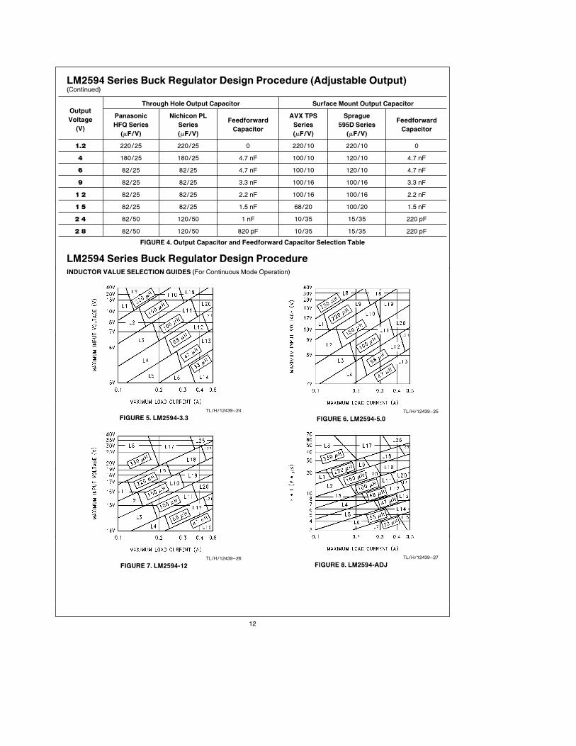
FIGURE 3. LM2594 Fixed Voltage Quick Design Component Selection Table
9
LM2594 Series Buck Regulator Design Procedure (Adjustable Output)
PROCEDURE (Adjustable Output Voltage Version) EXAMPLE (Adjustable Output Voltage Version)
Given: Given:
VOUT e Regulated Output Voltage VOUT e 20V
VIN(max) e Maximum Input Voltage VIN(max) e 28V
ILOAD(max) e Maximum Load Current ILOAD(max) e 0.5A
F e Switching Frequency (Fixed at a nominal 150 kHz). F e Switching Frequency (Fixed at a nominal 150 kHz).
1. Programming Output Voltage (Selecting R1 and R2, as 1. Programming Output Voltage (Selecting R1 and R2, as
shown in Figure 2 ) shown inFigure 2 )
Use the following formula to select the appropriate resis- Select R1 to be 1 kX, 1%. Solve for R2.tor values.
R2 e R1 #VOUT
VREF
b 1J e 1k # 20V
1.23Vb 1JVOUT e VREF #1 a
R2
R1 J where VREF e 1.23V
R2 e 1k (16.26 b 1) e 15.26k, closest 1% value isSelect a value for R1 between 240X and 1.5 kX. The
15.4 kX.lower resistor values minimize noise pickup in the sensi-
R2 e 15.4 kX.tive feedback pin. (For the lowest temperature coeffi-
cient and the best stability with time, use 1% metal film
resistors.)
R2 e R1 #VOUT
VREF
b 1J2. Inductor Selection (L1) 2. Inductor Selection (L1)
A. Calculate the inductor Volt microsecond constant A. Calculate the inductor Volt # microsecond constant
E # T (V # ms), from the following formula: (E # T),
E # T e (VIN b VOUT b VSAT) #VOUT a VD
VIN b VSAT a VD#
1000
150 kHz(V # ms) E # T e (28 b 20 b 0.9) #
20 a 0.5
28 b 0.9 a 0.5#
1000
150(V # ms)
where VSAT e internal switch saturation voltage e 0.9VE # T e (7.1) #
20.5
27.6# 6.67 (V # ms) e 35.2 (V # ms)
and VD e diode forward voltage drop e 0.5V
B. Use the E # T value from the previous formula and B. E # T e 35.2 (V # ms)
match it with the E # T number on the vertical axis of the C. ILOAD(max) e 0.5AInductor Value Selection Guide shown in Figure 8.
D. From the inductor value selection guide shown in Fig-C. on the horizontal axis, select the maximum load cur- ure 8, the inductance region intersected by the 35 (V #rent. ms) horizontal line and the 0.5A vertical line is 150 mH,
D. Identify the inductance region intersected by the E # T and the inductor code is L19.
value and the Maximum Load Current value. Each region E. From the table in Figure 9, locate line L19, and selectis identified by an inductance value and an inductor code an inductor part number from the list of manufacturers(LXX). part numbers.
E. Select an appropriate inductor from the four manufac-
turer’s part numbers listed in Figure 9.
3. Output Capacitor Selection (COUT) 3. Output Capacitor SeIection (COUT)
A. In the majority of applications, low ESR electrolytic or A. See section on COUT in Application Information sec-
solid tantalum capacitors between 82 mF and 220 mF tion.
provide the best results. This capacitor should be locat- B. From the quick design table shown in Figure 4, locateed close to the IC using short capacitor leads and short the output voltage column. From that column, locate thecopper traces. Do not use capacitors larger than 220 mF. output voltage closest to the output voltage in your appli-For additional information, see section on output ca- cation. In this example, select the 24V line. Under thepacitors in application information section. output capacitor section, select a capacitor from the list
B. To simplify the capacitor selection procedure, refer to of through hole electrolytic or surface mount tantalum
the quick design table shown in Figure 4. This table con- types from four different capacitor manufacturers. It is
tains different output voltages, and lists various output recommended that both the manufacturers and the man-
capacitors that will provide the best design solutions. ufacturers series that are listed in the table be used.
C. The capacitor voltage rating should be at least 1.5 In this example, through hole aluminum electrolytic ca-
times greater than the output voltage, and often much pacitors from several different manufacturers are avail-
higher voltage ratings are needed to satisfy the low ESR able.
requirements needed for low output ripple voltage. 82 mF 50V Panasonic HFQ Series
120 mF 50V Nichicon PL Series
Procedure continued on next page. Example continued on next page.
10
LM2594 Series Buck Regulator Design Procedure (Adjustable Output)
PROCEDURE (Adjustable Output Voltage Version) EXAMPLE (Adjustable Output Voltage Version)
4. Feedforward Capacitor (CFF) (SeeFigure 2 ) C. For a 20V output, a capacitor rating of at least 30V or
more is needed. In this example, either a 35V or 50VFor output voltages greater than approximately 10V, ancapacitor would work. A 50V rating was chosen becauseadditional capacitor is required. The compensation ca-it has a lower ESR which provides a lower output ripplepacitor is typically between 50 pF and 10 nF, and is wiredvoltage.in parallel with the output voltage setting resistor, R2. It
provides additional stability for high output voltages, low Other manufacturers or other types of capacitors may
input-output voltages, and/or very low ESR output ca- also be used, provided the capacitor specifications (es-
pacitors, such as solid tantalum capacitors. pecially the 100 kHz ESR) closely match the types listed
in the table. Refer to the capacitor manufacturers dataCFF e
1
31 c 103 c R2sheet for this information.
4. Feedforward Capacitor (CFF)This capacitor type can be ceramic, plastic, silver mica,
The table shown in Figure 4 contains feed forward ca-etc. (Because of the unstable characteristics of ceramicpacitor values for various output voltages. In this exam-capacitors made with Z5U material, they are not recom-ple, a 1 nF capacitor is needed.mended.)
5. Catch Diode Selection (D1)5. Catch Diode Selection (D1)
A. Refer to the table shown inFigure 12. Schottky diodesA. The catch diode current rating must be at least 1.3provide the best performance, and in this example a 1A,times greater than the maximum load current. Also, if the40V, 1N5819 Schottky diode would be a good choice.power supply design must withstand a continuous outputThe 1A diode rating is more than adequate and will notshort, the diode should have a current rating equal to thebe overstressed even for a shorted output.maximum current limit of the LM2594. The most stressful
condition for this diode is an overload or shorted output 6. Input Capacitor (CIN)
condition. The important parameters for the Input capacitor are the
B. The reverse voltage rating of the diode should be at input voltage rating and the RMS current rating. With a
least 1.25 times the maximum input voltage. nominal input voltage of 28V, an aluminum electrolytic
aluminum electrolytic capacitor with a voltage ratingC. This diode must be fast (short reverse recovery time)greater than 42V (1.5 c VIN) would be needed. Sinceand must be located close to the LM2594 using shortthe the next higher capacitor voltage rating is 50V, a 50Vleads and short printed circuit traces. Because of theircapacitor should be used. The capacitor voltage rating offast switching speed and low forward voltage drop,(1.5 c VIN) is a conservative guideline, and can be modi-Schottky diodes provide the best performance and effi-fied somewhat if desired.ciency, and should be the first choice, especially in low
output voltage applications. Ultra-fast recovery, or High- The RMS current rating requirement for the input capaci-
Efficiency rectifiers are also a good choice, but some tor of a buck regulator is approximately (/2 the DC load
types with an abrupt turn-off characteristic may cause current. In this example, with a 400 mA load, a capacitor
instability or EMl problems. Ultra-fast recovery diodes with a RMS current rating of at least 200 mA is needed.
typically have reverse recovery times of 50 ns or less. The curves shown in Figure 13 can be used to select anRectifiers such as the 1N4001 series are much too slow appropriate input capacitor. From the curves, locate theand should not be used. 50V line and note which capacitor values have RMS cur-
6. Input Capacitor (CIN) rent ratings greater than 200 mA. A 47 mF/50V low ESR
electrolytic capacitor capacitor is needed.A low ESR aluminum or tantalum bypass capacitor is
needed between the input pin and ground to prevent For a through hole design, a 47 mF/50V electrolytic ca-
large voltage transients from appearing at the input. In pacitor (Panasonic HFQ series or Nichicon PL series or
addition, the RMS current rating of the input capacitor equivalent) would be adequate. Other types or other
should be selected to be at least (/2 the DC load current. manufacturers capacitors can be used provided the
The capacitor manufacturers data sheet must be RMS ripple current ratings are adequate.
checked to assure that this current rating is not exceed- For surface mount designs, solid tantalum capacitors areed. The curve shown in Figure 13 shows typical RMS recommended. The TPS series available from AVX, andcurrent ratings for several different aluminum electrolytic the 593D series from Sprague are both surge currentcapacitor values. tested.
This capacitor should be located close to the IC using To further simplify the buck regulator design procedure, Na-short leads and the voltage rating should be approxi- tional Semiconductor is making available computer designmately 1.5 times the maximum input voltage. software to be used with the Simple Switcher line ot switch-If solid tantalum input capacitors are used, it is recom- ing regulators. Switchers Made Simple (version 4.1 or lat-ended that they be surge current tested by the manufac- er) is available on a 3(/2× diskette for IBM compatible com-turer. puters.
Use caution when using ceramic capacitors for input by-
passing, because it may cause severe ringing at the VINpin.
For additional information, see section on input capaci-
tors in application information section.
11
LM2594 Series Buck Regulator Design Procedure (Adjustable Output)(Continued)
Voltage
Output
(V)
Through Hole Output Capacitor Surface Mount Output Capacitor
Panasonic Nichicon PLFeedforward
AVX TPS SpragueFeedforward
HFQ Series SeriesCapacitor
Series 595D SeriesCapacitor
(mF/V) (mF/V) (mF/V) (mF/V)
1.2 220/25 220/25 0 220/10 220/10 0
4 180/25 180/25 4.7 nF 100/10 120/10 4.7 nF
6 82/25 82/25 4.7 nF 100/10 120/10 4.7 nF
9 82/25 82/25 3.3 nF 100/16 100/16 3.3 nF
1 2 82/25 82/25 2.2 nF 100/16 100/16 2.2 nF
1 5 82/25 82/25 1.5 nF 68/20 100/20 1.5 nF
2 4 82/50 120/50 1 nF 10/35 15/35 220 pF
2 8 82/50 120/50 820 pF 10/35 15/35 220 pF
FIGURE 4. Output Capacitor and Feedforward Capacitor Selection Table
LM2594 Series Buck Regulator Design ProcedureINDUCTOR VALUE SELECTION GUIDES (For Continuous Mode Operation)
TL/H/12439–24
FIGURE 5. LM2594-3.3TL/H/12439–25
FIGURE 6. LM2594-5.0
TL/H/12439–26
FIGURE 7. LM2594-12
TL/H/12439–27
FIGURE 8. LM2594-ADJ
12
LM2594 Series Buck Regulator Design Procedure (Continued)
Inductance
(mH)
Current
(A)
Schott Renco Pulse Engineering Coilcraft
Through Surface Through Surface Through Surface Surface
Hole Mount Hole Mount Hole Mount Mount
L1 220 0.18 67143910 67144280 RL-5470-3 RL1500-220 PE-53801 PE-53801-S DO1608-224
L2 150 0.21 67143920 67144290 RL-5470-4 RL1500-150 PE-53802 PE-53802-S DO1608-154
L3 100 0.26 67143930 67144300 RL-5470-5 RL1500-100 PE-53803 PE-53803-S DO1608-104
L4 68 0.32 67143940 67144310 RL-1284-68 RL1500-68 PE-53804 PE-53804-S DO1608-68
L5 47 0.37 67148310 67148420 RL-1284-47 RL1500-47 PE-53805 PE-53805-S DO1608-473
L6 33 0.44 67148320 67148430 RL-1284-33 RL1500-33 PE-53806 PE-53806-S DO1608-333
L7 22 0.60 67148330 67148440 RL-1284-22 RL1500-22 PE-53807 PE-53807-S DO1608-223
L8 330 0.26 67143950 67144320 RL-5470-2 RL1500-330 PE-53808 PE-53808-S DO3308-334
L9 220 0.32 67143960 67144330 RL-5470-3 RL1500-220 PE-53809 PE-53809-S DO3308-224
L10 150 0.39 67143970 67144340 RL-5470-4 RL1500-150 PE-53810 PE-53810-S DO3308-154
L11 100 0.48 67143980 67144350 RL-5470-5 RL1500-100 PE-53811 PE-53811-S DO3308-104
L12 68 0.58 67143990 67144360 RL-5470-6 RL1500-68 PE-53812 PE-53812-S DO1608-683
L13 47 0.70 67144000 67144380 RL-5470-7 RL1500-47 PE-53813 PE-53813-S DO3308-473
L14 33 0.83 67148340 67148450 RL-1284-33 RL1500-33 PE-53814 PE-53814-S DO1608-333
L15 22 0.99 67148350 67148460 RL-1284-22 RL1500-22 PE-53815 PE-53815-S DO1608-223
L16 15 1.24 67148360 67148470 RL-1284-15 RL1500-15 PE-53816 PE-53816-S DO1608-153
L17 330 0.42 67144030 67144410 RL-5471-1 RL1500-330 PE-53817 PE-53817-S DO3316-334
L18 220 0.55 67144040 67144420 RL-5471-2 RL1500-220 PE-53818 PE-53818-S DO3316-224
L19 150 0.66 67144050 67144430 RL-5471-3 RL1500-150 PE-53819 PE-53819-S DO3316-154
L20 100 0.82 67144060 67144440 RL-5471-4 RL1500-100 PE-53820 PE-53820-S DO3316-104
L21 68 0.99 67144070 67144450 RL-5471-5 RL1500-68 PE-53821 PE-53821-S DDO3316-683
L26 330 0.80 67144100 67144480 RL-5471-1 Ð PE-53826 PE-53826-S Ð
L27 220 1.00 67144110 67144490 RL-5471-2 Ð PE-53827 PE-53827-S Ð
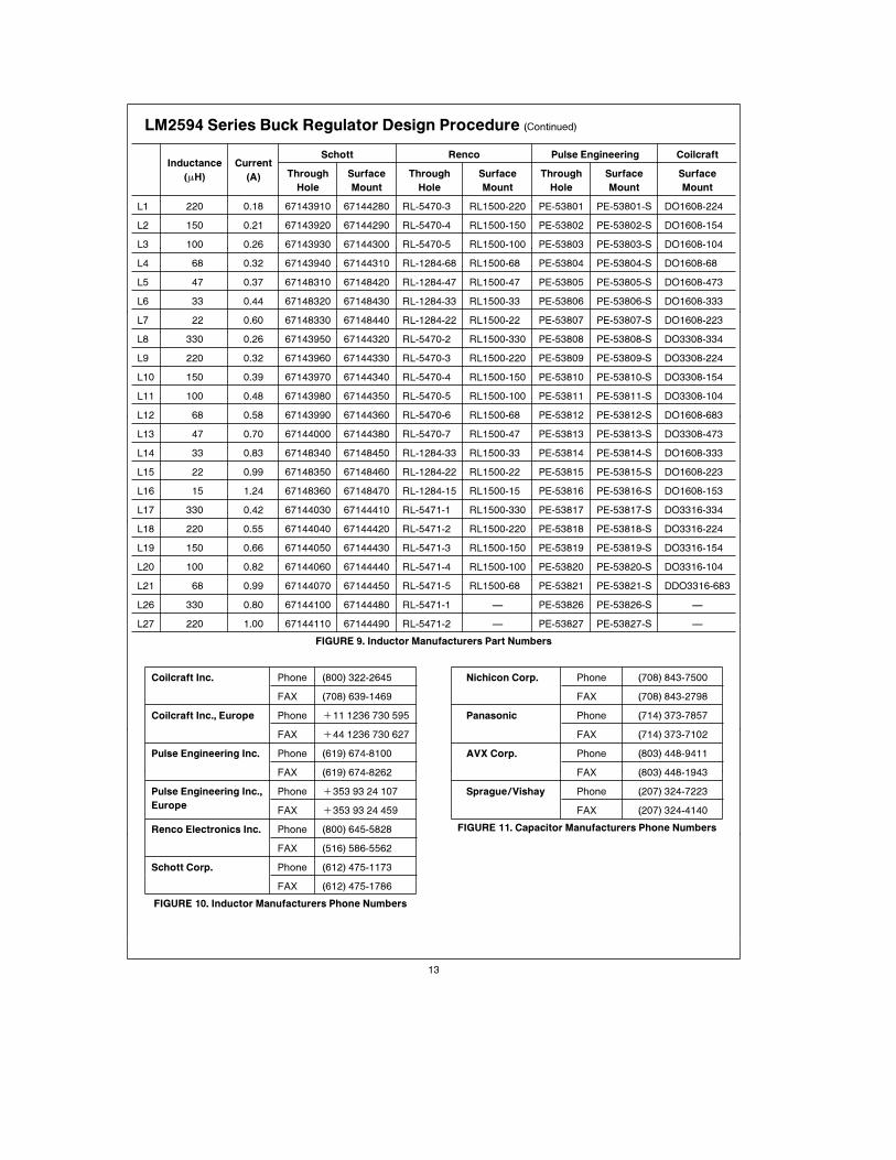
FIGURE 9. Inductor Manufacturers Part Numbers
Coilcraft Inc. Phone (800) 322-2645
FAX (708) 639-1469
Coilcraft Inc., Europe Phone a11 1236 730 595
FAX a44 1236 730 627
Pulse Engineering Inc. Phone (619) 674-8100
FAX (619) 674-8262
Pulse Engineering Inc., Phone a353 93 24 107
EuropeFAX a353 93 24 459
Renco Electronics Inc. Phone (800) 645-5828
FAX (516) 586-5562
Schott Corp. Phone (612) 475-1173
FAX (612) 475-1786
FIGURE 10. Inductor Manufacturers Phone Numbers
Nichicon Corp. Phone (708) 843-7500
FAX (708) 843-2798
Panasonic Phone (714) 373-7857
FAX (714) 373-7102
AVX Corp. Phone (803) 448-9411
FAX (803) 448-1943
Sprague/Vishay Phone (207) 324-7223
FAX (207) 324-4140
FIGURE 11. Capacitor Manufacturers Phone Numbers
13
LM2594 Series Buck RegulatorDesign Procedure (Continued)
VR
1A Diodes
Surface Mount Through Hole
SchottkyUltra Fast
SchottkyUltra Fast
Recovery Recovery
20VAll of 1N5817 All of
these theseSR102
diodes are diodes are
rated to at rated to atMBRS130 1N5818least 50V. least 50V.
30V SR103
11DQ03
MBRS140 MURS120 1N5819 MUR120
40V 10BQ040 10BF10 SR104 HER101
10MQ040 11DQ04 11DF1
more
50V
or
MBRS160 SR105
10BQ050 MBR150
10MQ060 11DQ05
FIGURE 12. Diode Selection Table
Application InformationPIN FUNCTIONS
aVINÐThis is the positive input supply for the IC switching
regulator. A suitable input bypass capacitor must be present
at this pin to minimize voltage transients and to supply the
switching currents needed by the regulator.
GroundÐCircuit ground.
OutputÐInternal switch. The voltage at this pin switches
between (aVIN b VSAT) and approximately b0.5V, with a
duty cycle of VOUT/VIN. To minimize coupling to sensitive
circuitry, the PC board copper area connected to this pin
should be kept to a minimum.
FeedbackÐSenses the regulated output voltage to com-
plete the feedback loop.
ON/OFFÐAllows the switching regulator circuit to be shut
down using logic level signals thus dropping the total input
supply current to approximately 80 mA. Pulling this pin be-
low a threshold voltage of approximately 1.3V turns the reg-
ulator on, and pulling this pin above 1.3V (up to a maximum
of 25V) shuts the regulator down. If this shutdown feature is
not needed, the ON/OFF pin can be wired to the ground pin
or it can be left open, in either case the regulator will be in
the ON condition.
EXTERNAL COMPONENTS
CINÐA low ESR aluminum or tantalum bypass capacitor is
needed between the input pin and ground pin. It must be
located near the regulator using short leads. This capacitor
prevents large voltage transients from appearing at the in-
put, and provides the instantaneous current needed each
time the switch turns on.
The important parameters for the Input capacitor are the
voltage rating and the RMS current rating. Because of the
relatively high RMS currents flowing in a buck regulator’s
input capacitor, this capacitor should be chosen for its RMS
current rating rather than its capacitance or voltage ratings,
although the capacitance value and voltage rating are di-
rectly related to the RMS current rating.
The RMS current rating of a capacitor could be viewed as a
capacitor’s power rating. The RMS current flowing through
the capacitors internal ESR produces power which causes
the internal temperature of the capacitor to rise. The RMS
current rating of a capacitor is determined by the amount of
current required to raise the internal temperature approxi-
mately 10§C above an ambient temperature of 105§C. The
ability of the capacitor to dissipate this heat to the surround-
ing air will determine the amount of current the capacitor
can safely sustain. Capacitors that are physically large and
have a large surface area will typically have higher RMS
current ratings. For a given capacitor value, a higher voltage
electrolytic capacitor will be physically larger than a lower
voltage capacitor, and thus be able to dissipate more heat
to the surrounding air, and therefore will have a higher RMS
current rating.
The consequences of operating an electrolytic capacitor
above the RMS current rating is a shortened operating life.
The higher temperature speeds up the evaporation of the
capacitor’s electrolyte, resulting in eventual failure.
Selecting an input capacitor requires consulting the manu-
facturers data sheet for maximum allowable RMS ripple cur-
rent. For a maximum ambient temperature of 40§C, a gener-
al guideline would be to select a capacitor with a ripple cur-
rent rating of approximately 50% of the DC load current. For
ambient temperatures up to 70§C, a current rating of 75% of
the DC load current would be a good choice for a conserva-
tive design. The capacitor voltage rating must be at least
1.25 times greater than the maximum input voltage, and of-
ten a much higher voltage capacitor is needed to satisfy the
RMS current requirements.
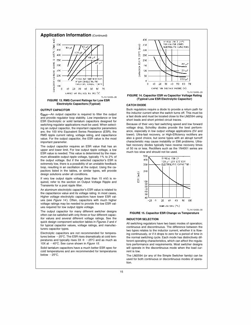
A graph shown in Figure 13 shows the relationship between
an electrolytic capacitor value, its voltage rating, and the
RMS current it is rated for. These curves were obtained
from the Nichicon ‘‘PL’’ series of low ESR, high reliability
electrolytic capacitors designed for switching regulator ap-
plications. Other capacitor manufacturers offer similar types
of capacitors, but always check the capacitor data sheet.
‘‘Standard’’ electrolytic capacitors typically have much high-
er ESR numbers, lower RMS current ratings and typically
have a shorter operating lifetime.
Because of their small size and excellent performance, sur-
face mount solid tantalum capacitors are often used for in-
put bypassing, but several precautions must be observed. A
small percentage of solid tantalum capacitors can short if
the inrush current rating is exceeded. This can happen at
turn on when the input voltage is suddenly applied, and of
course, higher input voltages produce higher inrush cur-
rents. Several capacitor manufacturers do a 100% surge
current testing on their products to minimize this potential
problem. If high turn on currents are expected, it may be
necessary to limit this current by adding either some resist-
ance or inductance before the tantalum capacitor, or select
a higher voltage capacitor. As with aluminum electrolytic ca-
pacitors, the RMS ripple current rating must be sized to the
load current.
14
Application Information (Continued)
TL/H/12439–28
FIGURE 13. RMS Current Ratings for Low ESR
Electrolytic Capacitors (Typical)
OUTPUT CAPACITOR
COUTÐAn output capacitor is required to filter the output
and provide regulator loop stability. Low impedance or low
ESR Electrolytic or solid tantalum capacitors designed for
switching regulator applications must be used. When select-
ing an output capacitor, the important capacitor parameters
are; the 100 kHz Equivalent Series Resistance (ESR), the
RMS ripple current rating, voltage rating, and capacitance
value. For the output capacitor, the ESR value is the most
important parameter.
The output capacitor requires an ESR value that has an
upper and lower limit. For low output ripple voltage, a low
ESR value is needed. This value is determined by the maxi-
mum allowable output ripple voltage, typically 1% to 2% of
the output voltage. But if the selected capacitor’s ESR is
extremely low, there is a possibility of an unstable feedback
loop, resulting in an oscillation at the output. Using the ca-
pacitors listed in the tables, or similar types, will provide
design solutions under all conditions.
If very low output ripple voltage (less than 15 mV) is re-
quired, refer to the section on Output Voltage Ripple and
Transients for a post ripple filter.
An aluminum electrolytic capacitor’s ESR value is related to
the capacitance value and its voltage rating. In most cases,
Higher voltage electrolytic capacitors have lower ESR val-
ues (see Figure 14 ). Often, capacitors with much higher
voltage ratings may be needed to provide the low ESR val-
ues required for low output ripple voltage.
The output capacitor for many different switcher designs
often can be satisfied with only three or four different capac-
itor values and several different voltage ratings. See the
quick design component selection tables in Figures 3 and 4for typical capacitor values, voltage ratings, and manufac-
turers capacitor types.
Electrolytic capacitors are not recommended for tempera-
tures below b25§C. The ESR rises dramatically at cold tem-
peratures and typically rises 3X @ b25§C and as much as
10X at b40§C. See curve shown in Figure 15.
Solid tantalum capacitors have a much better ESR spec for
cold temperatures and are recommended for temperatures
below b25§C.
TL/H/12439–29
FIGURE 14. Capacitor ESR vs Capacitor Voltage Rating
(Typical Low ESR Electrolytic Capacitor)
CATCH DIODE
Buck regulators require a diode to provide a return path for
the inductor current when the switch turns off. This must be
a fast diode and must be located close to the LM2594 using
short leads and short printed circuit traces.
Because of their very fast switching speed and low forward
voltage drop, Schottky diodes provide the best perform-
ance, especially in low output voltage applications (5V and
lower). Ultra-fast recovery, or High-Efficiency rectifiers are
also a good choice, but some types with an abrupt turnoff
characteristic may cause instability or EMI problems. Ultra-
fast recovery diodes typically have reverse recovery times
of 50 ns or less. Rectifiers such as the 1N4001 series are
much too slow and should not be used.
TL/H/12439–30
FIGURE 15. Capacitor ESR Change vs Temperature
INDUCTOR SELECTION
All switching regulators have two basic modes of operation;
continuous and discontinuous. The difference between the
two types relates to the inductor current, whether it is flow-
ing continuously, or if it drops to zero for a period of time in
the normal switching cycle. Each mode has distinctively dif-
ferent operating characteristics, which can affect the regula-
tors performance and requirements. Most switcher designs
will operate in the discontinuous mode when the load cur-
rent is low.
The LM2594 (or any of the Simple Switcher family) can be
used for both continuous or discontinuous modes of opera-
tion.
15
Application Information (Continued)
In many cases the preferred mode of operation is the con-
tinuous mode. It offers greater output power, lower peak
switch, inductor and diode currents, and can have lower out-
put ripple voltage. But it does require larger inductor values
to keep the inductor current flowing continuously, especially
at low output load currents and/or high input voltages.
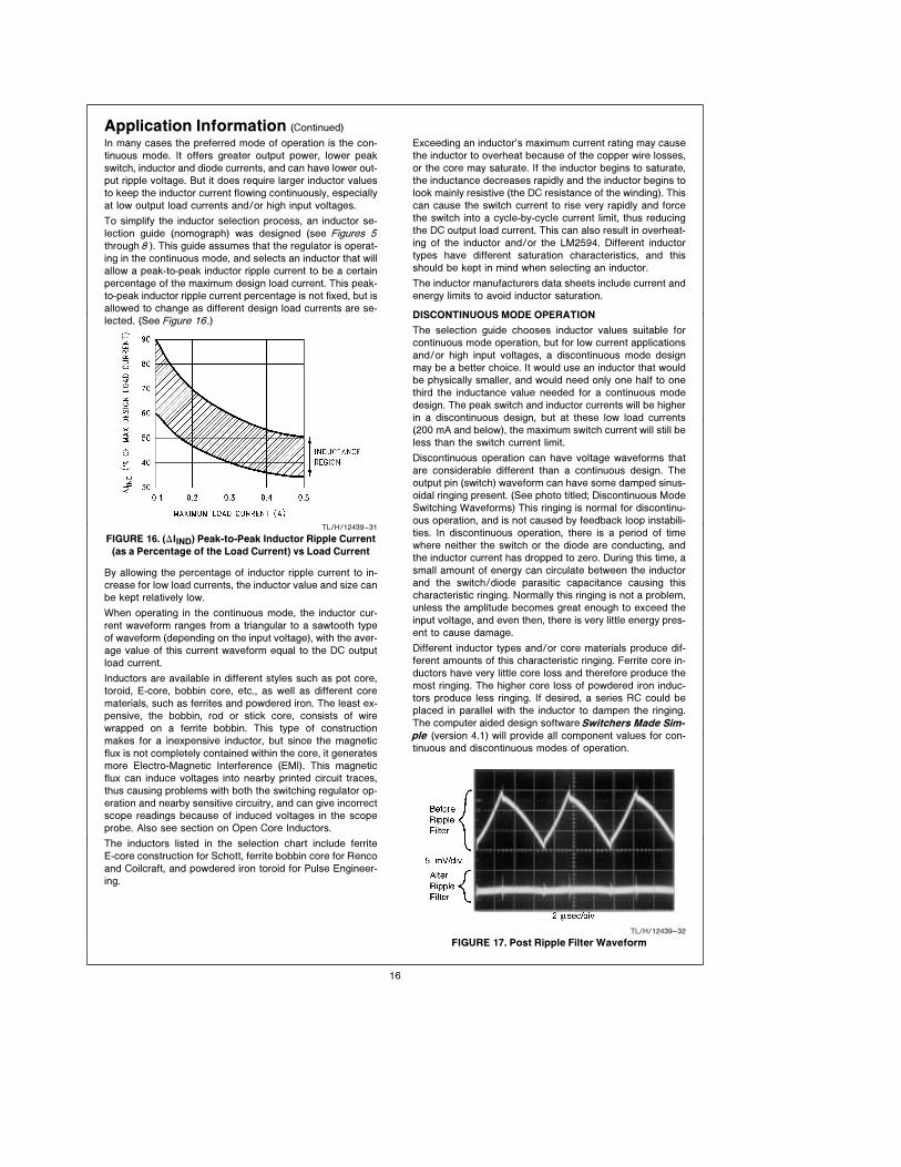
To simplify the inductor selection process, an inductor se-
lection guide (nomograph) was designed (see Figures 5through 8 ). This guide assumes that the regulator is operat-
ing in the continuous mode, and selects an inductor that will
allow a peak-to-peak inductor ripple current to be a certain
percentage of the maximum design load current. This peak-
to-peak inductor ripple current percentage is not fixed, but is
allowed to change as different design load currents are se-
lected. (See Figure 16.)
TL/H/12439–31
FIGURE 16. (DIIND) Peak-to-Peak Inductor Ripple Current
(as a Percentage of the Load Current) vs Load Current
By allowing the percentage of inductor ripple current to in-
crease for low load currents, the inductor value and size can
be kept relatively low.
When operating in the continuous mode, the inductor cur-
rent waveform ranges from a triangular to a sawtooth type
of waveform (depending on the input voltage), with the aver-
age value of this current waveform equal to the DC output
load current.
Inductors are available in different styles such as pot core,
toroid, E-core, bobbin core, etc., as well as different core
materials, such as ferrites and powdered iron. The least ex-
pensive, the bobbin, rod or stick core, consists of wire
wrapped on a ferrite bobbin. This type of construction
makes for a inexpensive inductor, but since the magnetic
flux is not completely contained within the core, it generates
more Electro-Magnetic Interference (EMl). This magnetic
flux can induce voltages into nearby printed circuit traces,
thus causing problems with both the switching regulator op-
eration and nearby sensitive circuitry, and can give incorrect
scope readings because of induced voltages in the scope
probe. Also see section on Open Core Inductors.
The inductors listed in the selection chart include ferrite
E-core construction for Schott, ferrite bobbin core for Renco
and Coilcraft, and powdered iron toroid for Pulse Engineer-
ing.
Exceeding an inductor’s maximum current rating may cause
the inductor to overheat because of the copper wire losses,
or the core may saturate. If the inductor begins to saturate,
the inductance decreases rapidly and the inductor begins to
look mainly resistive (the DC resistance of the winding). This
can cause the switch current to rise very rapidly and force
the switch into a cycle-by-cycle current limit, thus reducing
the DC output load current. This can also result in overheat-
ing of the inductor and/or the LM2594. Different inductor
types have different saturation characteristics, and this
should be kept in mind when selecting an inductor.
The inductor manufacturers data sheets include current and
energy limits to avoid inductor saturation.
DISCONTINUOUS MODE OPERATION
The selection guide chooses inductor values suitable for
continuous mode operation, but for low current applications
and/or high input voltages, a discontinuous mode design
may be a better choice. It would use an inductor that would
be physically smaller, and would need only one half to one
third the inductance value needed for a continuous mode
design. The peak switch and inductor currents will be higher
in a discontinuous design, but at these low load currents
(200 mA and below), the maximum switch current will still be
less than the switch current limit.
Discontinuous operation can have voltage waveforms that
are considerable different than a continuous design. The
output pin (switch) waveform can have some damped sinus-
oidal ringing present. (See photo titled; Discontinuous Mode
Switching Waveforms) This ringing is normal for discontinu-
ous operation, and is not caused by feedback loop instabili-
ties. In discontinuous operation, there is a period of time
where neither the switch or the diode are conducting, and
the inductor current has dropped to zero. During this time, a
small amount of energy can circulate between the inductor
and the switch/diode parasitic capacitance causing this
characteristic ringing. Normally this ringing is not a problem,
unless the amplitude becomes great enough to exceed the
input voltage, and even then, there is very little energy pres-
ent to cause damage.
Different inductor types and/or core materials produce dif-
ferent amounts of this characteristic ringing. Ferrite core in-
ductors have very little core loss and therefore produce the
most ringing. The higher core loss of powdered iron induc-
tors produce less ringing. If desired, a series RC could be
placed in parallel with the inductor to dampen the ringing.
The computer aided design softwareSwitchers Made Sim-ple (version 4.1) will provide all component values for con-
tinuous and discontinuous modes of operation.
TL/H/12439–32
FIGURE 17. Post Ripple Filter Waveform
16
Application Information (Continued)
OUTPUT VOLTAGE RIPPLE AND TRANSIENTS
The output voltage of a switching power supply operating in
the continuous mode will contain a sawtooth ripple voltage
at the switcher frequency, and may also contain short volt-
age spikes at the peaks of the sawtooth waveform.
The output ripple voltage is a function of the inductor saw-
tooth ripple current and the ESR of the output capacitor. A
typical output ripple voltage can range from approximately
0.5% to 3% of the output voltage. To obtain low ripple volt-
age, the ESR of the output capacitor must be low, however,
caution must be exercised when using extremely low ESR
capacitors because they can affect the loop stability, result-
ing in oscillation problems. If very low output ripple voltage
is needed (less than 15 mV), a post ripple filter is recom-
mended. (SeeFigure 2.) The inductance required is typically
between 1 mH and 5 mH, with low DC resistance, to main-
tain good load regulation. A low ESR output filter capacitor
is also required to assure good dynamic load response and
ripple reduction. The ESR of this capacitor may be as low as
desired, because it is out of the regulator feedback loop.
The photo shown in Figure 17 shows a typical output ripple
voltage, with and without a post ripple filter.
When observing output ripple with a scope, it is essential
that a short, low inductance scope probe ground connection
be used. Most scope probe manufacturers provide a special
probe terminator which is soldered onto the regulator board,
preferable at the output capacitor. This provides a very
short scope ground thus eliminating the problems associat-
ed with the 3 inch ground lead normally provided with the
probe, and provides a much cleaner and more accurate pic-
ture of the ripple voltage waveform.
The voltage spikes are caused by the fast switching action
of the output switch and the diode, and the parasitic induc-
tance of the output filter capacitor, and its associated wiring.
To minimize these voltage spikes, the output capacitor
should be designed for switching regulator applications, and
the lead lengths must be kept very short. Wiring inductance,
stray capacitance, as well as the scope probe used to eval-
uate these transients, all contribute to the amplitude of
these spikes.
When a switching regulator is operating in the continuous
mode, the inductor current waveform ranges from a triangu-
lar to a sawtooth type of waveform (depending on the input
voltage). For a given input and output voltage, the peak-to-
peak amplitude of this inductor current waveform remains
constant. As the load current increases or decreases, the
entire sawtooth current waveform also rises and falls. The
average value (or the center) of this current waveform is
equal to the DC load current.
If the load current drops to a low enough level, the bottom
of the sawtooth current waveform will reach zero, and the
switcher will smoothly change from a continuous to a dis-
continuous mode of operation. Most switcher designs (irre-
gardless how large the inductor value is) will be forced to
run discontinuous if the output is lightly loaded. This is a
perfectly acceptable mode of operation.
TL/H/12439–33
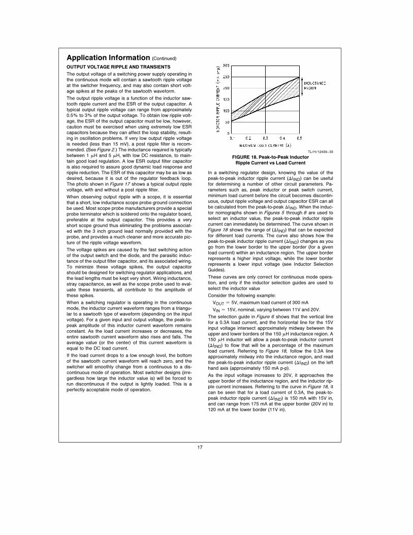
FIGURE 18. Peak-to-Peak Inductor
Ripple Current vs Load Current
In a switching regulator design, knowing the value of the
peak-to-peak inductor ripple current (DIIND) can be useful
for determining a number of other circuit parameters. Pa-
rameters such as, peak inductor or peak switch current,
minimum load current before the circuit becomes discontin-
uous, output ripple voltage and output capacitor ESR can all
be calculated from the peak-to-peak DIIND. When the induc-
tor nomographs shown in Figures 5 through 8 are used to
select an inductor value, the peak-to-peak inductor ripple
current can immediately be determined. The curve shown in
Figure 18 shows the range of (DIIND) that can be expected
for different load currents. The curve also shows how the
peak-to-peak inductor ripple current (DIIND) changes as you
go from the lower border to the upper border (for a given
load current) within an inductance region. The upper border
represents a higher input voltage, while the lower border
represents a lower input voltage (see Inductor Selection
Guides).
These curves are only correct for continuous mode opera-
tion, and only if the inductor selection guides are used to
select the inductor value
Consider the following example:
VOUT e 5V, maximum load current of 300 mA
VIN e 15V, nominal, varying between 11V and 20V.
The selection guide in Figure 6 shows that the vertical line
for a 0.3A load current, and the horizontal line for the 15V
input voltage intersect approximately midway between the
upper and lower borders of the 150 mH inductance region. A
150 mH inductor will allow a peak-to-peak inductor current
(DIIND) to flow that will be a percentage of the maximum
load current. Referring to Figure 18, follow the 0.3A line
approximately midway into the inductance region, and read
the peak-to-peak inductor ripple current (DIIND) on the left
hand axis (approximately 150 mA p-p).
As the input voltage increases to 20V, it approaches the
upper border of the inductance region, and the inductor rip-
ple current increases. Referring to the curve in Figure 18, it
can be seen that for a load current of 0.3A, the peak-to-
peak inductor ripple current (DIIND) is 150 mA with 15V in,
and can range from 175 mA at the upper border (20V in) to
120 mA at the lower border (11V in).
17
Application Information (Continued)
Once the DIIND value is known, the following formulas can
be used to calculate additional information about the switch-
ing regulator circuit.
1. Peak Inductor or peak switch current
e # ILOAD a
DIIND
2 J e #0.3A a
0.150
2 J e 0.375A
2. Minimum load current before the circuit becomes discon-
tinuous
e
DIIND
2e
0.150
2e 0.075A
3. Output Ripple Voltage e (DIIND)c(ESR of COUT)
e 0.150Ac0.240Xe36 mV p-p
or
4. ESR of COUT e
Output Ripple Voltage (DVOUT)
DIIND
e
0.036V
0.150Ae 0.240X
OPEN CORE INDUCTORS
Another possible source of increased output ripple voltage
or unstable operation is from an open core inductor. Ferrite
bobbin or stick inductors have magnetic lines of flux flowing
through the air from one end of the bobbin to the other end.
These magnetic lines of flux will induce a voltage into any
wire or PC board copper trace that comes within the induc-
tor’s magnetic field. The strength of the magnetic field, the
orientation and location of the PC copper trace to the mag-
netic field, and the distance between the copper trace and
the inductor, determine the amount of voltage generated in
the copper trace. Another way of looking at this inductive
coupling is to consider the PC board copper trace as one
turn of a transformer (secondary) with the inductor winding
as the primary. Many millivolts can be generated in a copper
trace located near an open core inductor which can cause
stability problems or high output ripple voltage problems.
If unstable operation is seen, and an open core inductor is
used, it’s possible that the location of the inductor with re-
spect to other PC traces may be the problem. To determine
if this is the problem, temporarily raise the inductor away
from the board by several inches and then check circuit
operation. If the circuit now operates correctly, then the
magnetic flux from the open core inductor is causing the
problem. Substituting a closed core inductor such as a tor-
roid or E-core will correct the problem, or re-arranging the
PC layout may be necessary. Magnetic flux cutting the IC
device ground trace, feedback trace, or the positive or neg-
ative traces of the output capacitor should be minimized.
Sometimes, locating a trace directly beneath a bobbin in-
ductor will provide good results, provided it is exactly in the
center of the inductor (because the induced voltages cancel
themselves out), but if it is off center one direction or the
other, then problems could arise. If flux problems are pres-
ent, even the direction of the inductor winding can make a
difference in some circuits.
This discussion on open core inductors is not to frighten the
user, but to alert the user on what kind of problems to watch
out for when using them. Open core bobbin or ‘‘stick’’ induc-
tors are an inexpensive, simple way of making a compact
efficient inductor, and they are used by the millions in many
different applications.
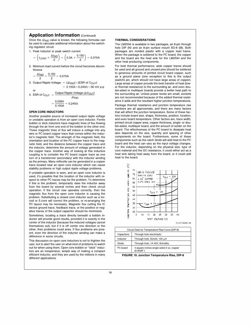
THERMAL CONSIDERATIONS
The LM2594 is available in two packages, an 8-pin through
hole DIP (N) and an 8-pin surface mount SO-8 (M). Both
packages are molded plastic with a copper lead frame.
When the package is soldered to the PC board, the copper
and the board are the heat sink for the LM2594 and the
other heat producing components.
For best thermal performance, wide copper traces should
be used and all ground and unused pins should be soldered
to generous amounts of printed circuit board copper, such
as a ground plane (one exception to this is the output
(switch) pin, which should not have large areas of copper).
Large areas of copper provide the best transfer of heat (low-
er thermal resistance) to the surrounding air, and even dou-
ble-sided or multilayer boards provide a better heat path to
the surrounding air. Unless power levels are small, sockets
are not recommended because of the added thermal resist-
ance it adds and the resultant higher junction temperatures.
Package thermal resistance and junction temperature rise
numbers are all approximate, and there are many factors
that will affect the junction temperature. Some of these fac-
tors include board size, shape, thickness, position, location,
and even board temperature. Other factors are, trace width,
printed circuit copper area, copper thickness, single- or dou-
ble-sided, multilayer board, and the amount of solder on the
board. The effectiveness of the PC board to dissipate heat
also depends on the size, quantity and spacing of other
components on the board. Furthermore, some of these
components such as the catch diode will add heat to the PC
board and the heat can vary as the input voltage changes.
For the inductor, depending on the physical size, type of
core material and the DC resistance, it could either act as a
heat sink taking heat away from the board, or it could add
heat to the board.
TL/H/12439–35
Circuit Data for Temperature Rise Curve (DIP-8)
Capacitors Through hole electrolytic
Inductor Through hole, Schott, 100 mH
Diode Through hole, 1A 40V, Schottky
PC board 4 square inches single sided 2 oz. copper(0.0028×)
FIGURE 19. Junction Temperature Rise, DIP-8
18
Application Information (Continued)
TL/H/12439–34
Circuit Data for Temperature Rise Curve (Surface Mount)
Capacitors Surface mount tantalum, molded ‘‘D’’ size
Inductor Surface mount, Coilcraft DO33, 100 mH
Diode Surface mount, 1A 40V, Schottky
PC board 4 square inches single sided 2 oz. copper
(0.0028×)
FIGURE 20. Junction Temperature Rise, SO-8
The curves shown in Figures 19 and 20 show the LM2594
junction temperature rise above ambient temperature with a
500 mA load for various input and output voltages. This data
was taken with the circuit operating as a buck switcher with
all components mounted on a PC board to simulate the
junction temperature under actual operating conditions. This
curve is typical, and can be used for a quick check on the
maximum junction temperature for various conditions, but
keep in mind that there are many factors that can affect the
junction temperature.
TL/H/12439–36
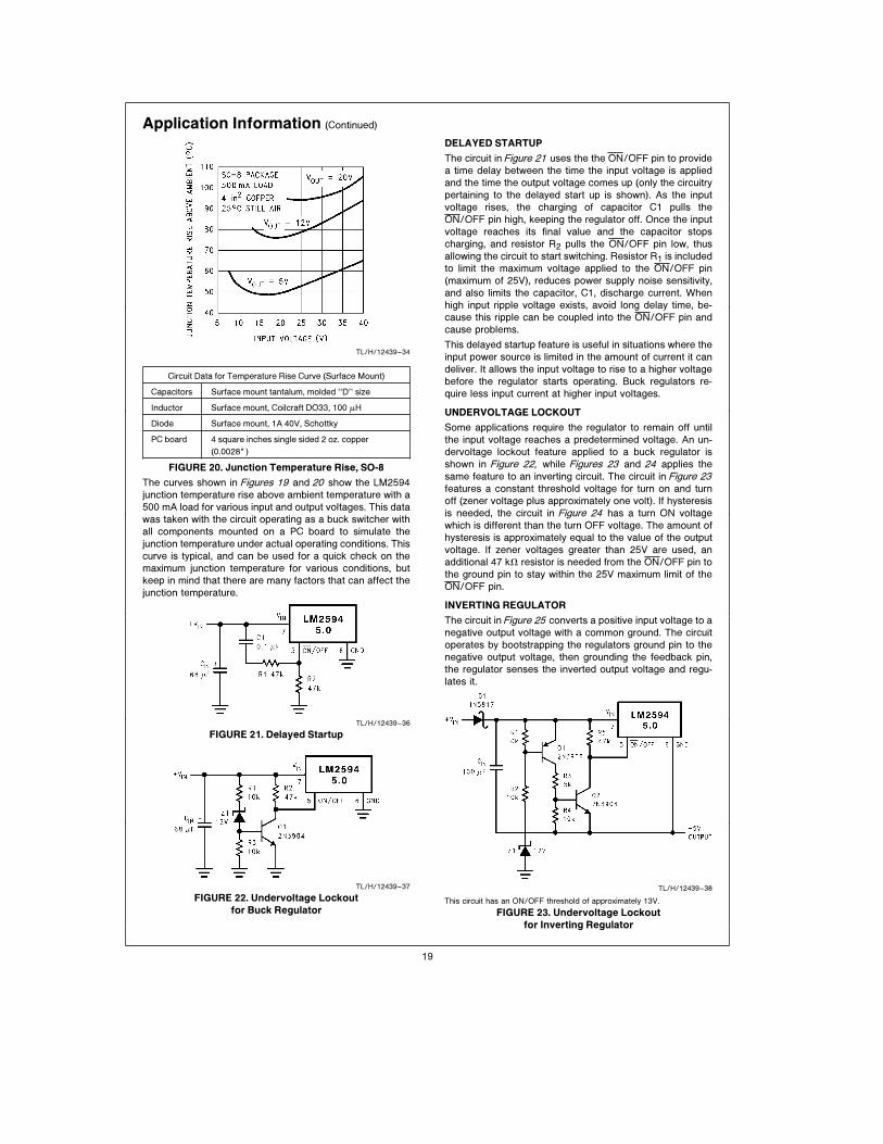
FIGURE 21. Delayed Startup
TL/H/12439–37
FIGURE 22. Undervoltage Lockout
for Buck Regulator
DELAYED STARTUP
The circuit in Figure 21 uses the the ON/OFF pin to provide
a time delay between the time the input voltage is applied
and the time the output voltage comes up (only the circuitry
pertaining to the delayed start up is shown). As the input
voltage rises, the charging of capacitor C1 pulls the
ON/OFF pin high, keeping the regulator off. Once the input
voltage reaches its final value and the capacitor stops
charging, and resistor R2 pulls the ON/OFF pin low, thus
allowing the circuit to start switching. Resistor R1 is included
to limit the maximum voltage applied to the ON/OFF pin
(maximum of 25V), reduces power supply noise sensitivity,
and also limits the capacitor, C1, discharge current. When
high input ripple voltage exists, avoid long delay time, be-
cause this ripple can be coupled into the ON/OFF pin and
cause problems.
This delayed startup feature is useful in situations where the
input power source is limited in the amount of current it can
deliver. It allows the input voltage to rise to a higher voltage
before the regulator starts operating. Buck regulators re-
quire less input current at higher input voltages.
UNDERVOLTAGE LOCKOUT
Some applications require the regulator to remain off until
the input voltage reaches a predetermined voltage. An un-
dervoltage lockout feature applied to a buck regulator is
shown in Figure 22, while Figures 23 and 24 applies the
same feature to an inverting circuit. The circuit in Figure 23features a constant threshold voltage for turn on and turn
off (zener voltage plus approximately one volt). If hysteresis
is needed, the circuit in Figure 24 has a turn ON voltage
which is different than the turn OFF voltage. The amount of
hysteresis is approximately equal to the value of the output
voltage. If zener voltages greater than 25V are used, an
additional 47 kX resistor is needed from the ON/OFF pin to
the ground pin to stay within the 25V maximum limit of the
ON/OFF pin.
INVERTING REGULATOR
The circuit inFigure 25 converts a positive input voltage to a
negative output voltage with a common ground. The circuit
operates by bootstrapping the regulators ground pin to the
negative output voltage, then grounding the feedback pin,
the regulator senses the inverted output voltage and regu-
lates it.
TL/H/12439–38
This circuit has an ON/OFF threshold of approximately 13V.
FIGURE 23. Undervoltage Lockout
for Inverting Regulator
19
Application Information (Continued)
This circuit has hysteresis
Regulator starts switching at VIN e 13VTL/H/12439–39
Regulator stops switching at VIN e 8V
FIGURE 24. Undervoltage Lockout with Hysteresis for Inverting Regulator
CIN Ð 68 mF/25V Tant. Sprague 595D
120 mF/35V Elec. Panasonic HFQ
COUT Ð 22 mF/20V Tant. Sprague 595DTL/H/12439–40
39 mF/16V Elec. Panasonic HFQ
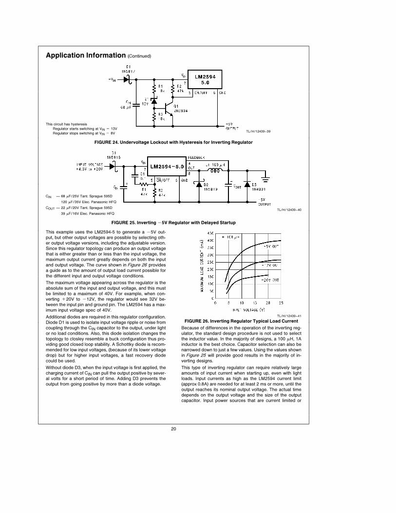
FIGURE 25. Inverting b5V Regulator with Delayed Startup
This example uses the LM2594-5 to generate a b5V out-
put, but other output voltages are possible by selecting oth-
er output voltage versions, including the adjustable version.
Since this regulator topology can produce an output voltage
that is either greater than or less than the input voltage, the
maximum output current greatly depends on both the input
and output voltage. The curve shown in Figure 26 provides
a guide as to the amount of output load current possible for
the different input and output voltage conditions.
The maximum voltage appearing across the regulator is the
absolute sum of the input and output voltage, and this must
be limited to a maximum of 40V. For example, when con-
verting a20V to b12V, the regulator would see 32V be-
tween the input pin and ground pin. The LM2594 has a max-
imum input voltage spec of 40V.
Additional diodes are required in this regulator configuration.
Diode D1 is used to isolate input voltage ripple or noise from
coupling through the CIN capacitor to the output, under light
or no load conditions. Also, this diode isolation changes the
topology to closley resemble a buck configuration thus pro-
viding good closed loop stability. A Schottky diode is recom-
mended for low input voltages, (because of its lower voltage
drop) but for higher input voltages, a fast recovery diode
could be used.
Without diode D3, when the input voltage is first applied, the
charging current of CIN can pull the output positive by sever-
al volts for a short period of time. Adding D3 prevents the
output from going positive by more than a diode voltage.
TL/H/12439–41
FIGURE 26. Inverting Regulator Typical Load Current
Because of differences in the operation of the inverting reg-
ulator, the standard design procedure is not used to select
the inductor value. In the majority of designs, a 100 mH, 1A
inductor is the best choice. Capacitor selection can also be
narrowed down to just a few values. Using the values shown
in Figure 25 will provide good results in the majority of in-
verting designs.
This type of inverting regulator can require relatively large
amounts of input current when starting up, even with light
loads. Input currents as high as the LM2594 current limit
(approx 0.8A) are needed for at least 2 ms or more, until the
output reaches its nominal output voltage. The actual time
depends on the output voltage and the size of the output
capacitor. Input power sources that are current limited or
20
Application Information (Continued)
sources that can not deliver these currents without getting
loaded down, may not work correctly. Because of the rela-
tively high startup currents required by the inverting topolo-
gy, the delayed startup feature (C1, R1 and R2) shown in
Figure 25 is recommended. By delaying the regulator start-
up, the input capacitor is allowed to charge up to a higher
voltage before the switcher begins operating. A portion of
the high input current needed for startup is now supplied by
the input capacitor (CIN). For severe start up conditions, the
input capacitor can be made much larger than normal.
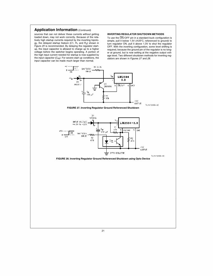
INVERTING REGULATOR SHUTDOWN METHODS
To use the ON/OFF pin in a standard buck configuration is
simple, pull it below 1.3V (@25§C, referenced to ground) to
turn regulator ON, pull it above 1.3V to shut the regulator
OFF. With the inverting configuration, some level shifting is
required, because the ground pin of the regulator is no long-
er at ground, but is now setting at the negative output volt-
age level. Two different shutdown methods for inverting reg-
ulators are shown in Figures 27 and 28.
TL/H/12439–42
FIGURE 27. Inverting Regulator Ground Referenced Shutdown
TL/H/12439–43
FIGURE 28. Inverting Regulator Ground Referenced Shutdown using Opto Device
21
Application Information (Continued)
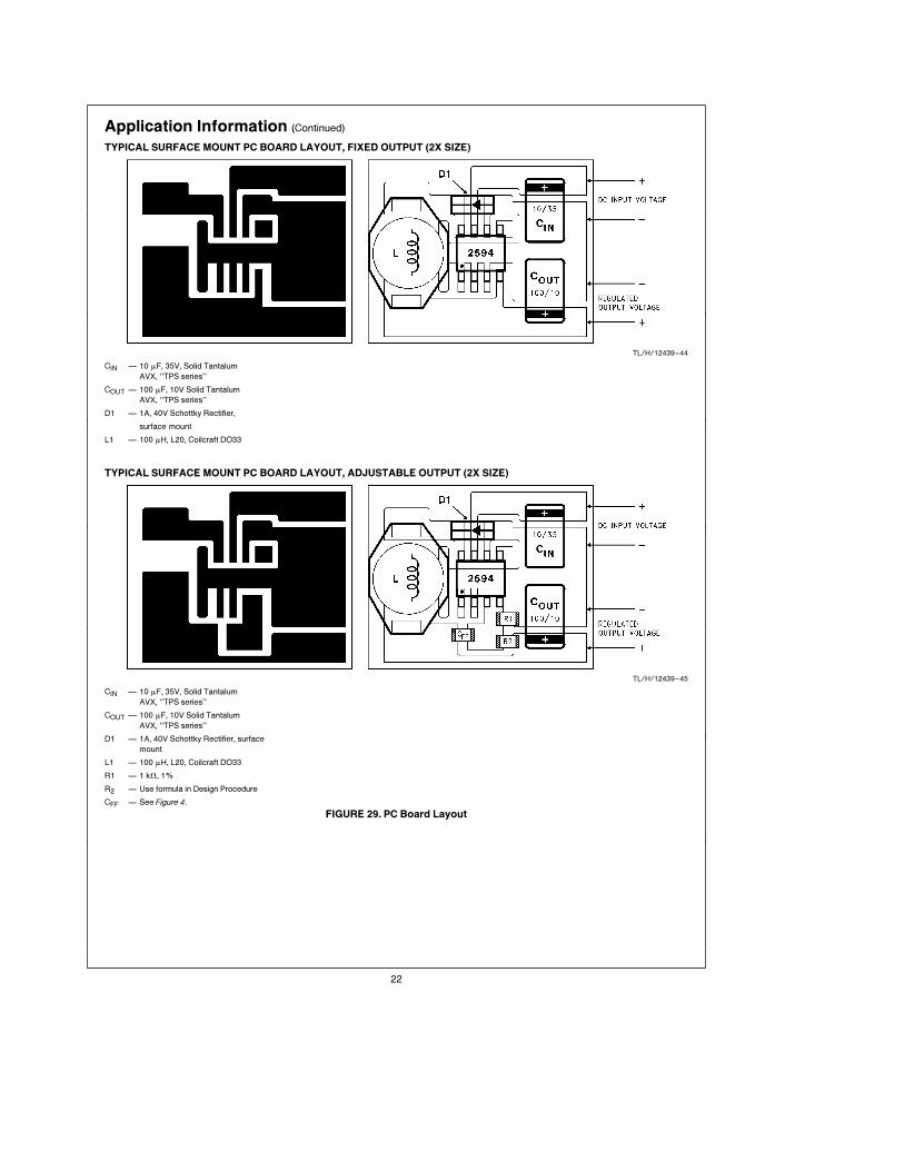
TYPICAL SURFACE MOUNT PC BOARD LAYOUT, FIXED OUTPUT (2X SIZE)
TL/H/12439–44
CIN Ð 10 mF, 35V, Solid Tantalum
AVX, ‘‘TPS series’’
COUT Ð 100 mF, 10V Solid Tantalum
AVX, ‘‘TPS series’’
D1 Ð 1A, 40V Schottky Rectifier,
surface mount
L1 Ð 100 mH, L20, Coilcraft DO33
TYPICAL SURFACE MOUNT PC BOARD LAYOUT, ADJUSTABLE OUTPUT (2X SIZE)
TL/H/12439–45
CIN Ð 10 mF, 35V, Solid Tantalum
AVX, ‘‘TPS series’’
COUT Ð 100 mF, 10V Solid Tantalum
AVX, ‘‘TPS series’’
D1 Ð 1A, 40V Schottky Rectifier, surface
mount
L1 Ð 100 mH, L20, Coilcraft DO33
R1 Ð 1 kX, 1%
R2 Ð Use formula in Design Procedure
CFF Ð SeeFigure 4.
FIGURE 29. PC Board Layout
22
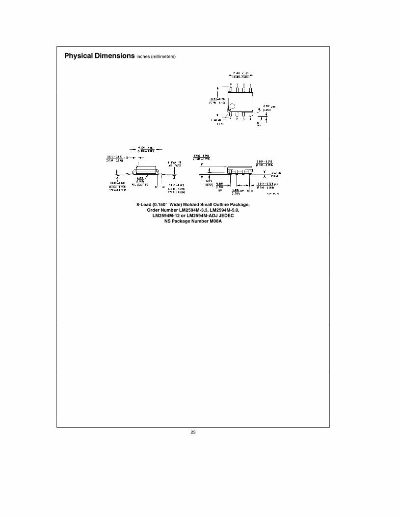
Physical Dimensions inches (millimeters)
8-Lead (0.150× Wide) Molded Small Outline Package,
Order Number LM2594M-3.3, LM2594M-5.0,
LM2594M-12 or LM2594M-ADJ JEDEC
NS Package Number M08A
23
LM
2594
SIM
PLE
SW
ITC
HER
Pow
erC
onvert
er150
kH
z0.5
ASte
p-D
ow
nV
oltage
Regula
tor
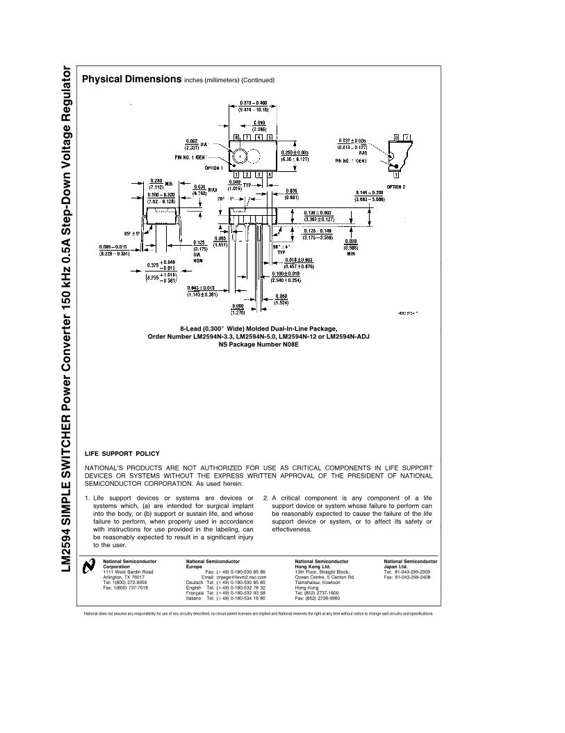
Physical Dimensions inches (millimeters) (Continued)
8-Lead (0.300× Wide) Molded Dual-In-Line Package,
Order Number LM2594N-3.3, LM2594N-5.0, LM2594N-12 or LM2594N-ADJ
NS Package Number N08E
LIFE SUPPORT POLICY
NATIONAL’S PRODUCTS ARE NOT AUTHORIZED FOR USE AS CRITICAL COMPONENTS IN LIFE SUPPORT
DEVICES OR SYSTEMS WITHOUT THE EXPRESS WRITTEN APPROVAL OF THE PRESIDENT OF NATIONAL
SEMICONDUCTOR CORPORATION. As used herein:
1. Life support devices or systems are devices or 2. A critical component is any component of a life
systems which, (a) are intended for surgical implant support device or system whose failure to perform can
into the body, or (b) support or sustain life, and whose be reasonably expected to cause the failure of the life
failure to perform, when properly used in accordance support device or system, or to affect its safety or
with instructions for use provided in the labeling, can effectiveness.
be reasonably expected to result in a significant injury
to the user.
National Semiconductor National Semiconductor National Semiconductor National SemiconductorCorporation Europe Hong Kong Ltd. Japan Ltd.1111 West Bardin Road Fax: (a49) 0-180-530 85 86 13th Floor, Straight Block, Tel: 81-043-299-2309Arlington, TX 76017 Email: cnjwge@ tevm2.nsc.com Ocean Centre, 5 Canton Rd. Fax: 81-043-299-2408Tel: 1(800) 272-9959 Deutsch Tel: (a49) 0-180-530 85 85 Tsimshatsui, KowloonFax: 1(800) 737-7018 English Tel: (a49) 0-180-532 78 32 Hong Kong
Fran3ais Tel: (a49) 0-180-532 93 58 Tel: (852) 2737-1600Italiano Tel: (a49) 0-180-534 16 80 Fax: (852) 2736-9960
National does not assume any responsibility for use of any circuitry described, no circuit patent licenses are implied and National reserves the right at any time without notice to change said circuitry and specifications.
Recommended