LM118/LM218/LM318Operational AmplifiersGeneral DescriptionThe LM118 series are precision high speed operational am-plifiers designed for applications requiring wide bandwidthand high slew rate. They feature a factor of ten increase inspeed over general purpose devices without sacrificing DCperformance.
The LM118 series has internal unity gain frequency compen-sation. This considerably simplifies its application since noexternal components are necessary for operation. However,unlike most internally compensated amplifiers, external fre-quency compensation may be added for optimum perfor-mance. For inverting applications, feedforward compensa-tion will boost the slew rate to over 150V/µs and almostdouble the bandwidth. Overcompensation can be used withthe amplifier for greater stability when maximum bandwidthis not needed. Further, a single capacitor can be added to re-duce the 0.1% settling time to under 1 µs.
The high speed and fast settling time of these op amps makethem useful in A/D converters, oscillators, active filters,
sample and hold circuits, or general purpose amplifiers.These devices are easy to apply and offer an order of mag-nitude better AC performance than industry standards suchas the LM709.
The LM218 is identical to the LM118 except that the LM218has its performance specified over a −25˚C to +85˚C tem-perature range. The LM318 is specified from 0˚C to +70˚C.
Featuresn 15 MHz small signal bandwidthn Guaranteed 50V/µs slew raten Maximum bias current of 250 nAn Operates from supplies of ±5V to ±20Vn Internal frequency compensationn Input and output overload protectedn Pin compatible with general purpose op amps
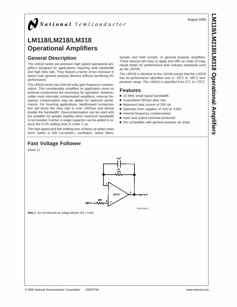
Fast Voltage Follower(Note 1)
DS007766-13
Note 1: Do not hard-wire as voltage follower (R1 ≥ 5 kΩ)
August 2000LM
118/LM218/LM
318O
perationalAm
plifiers
© 2000 National Semiconductor Corporation DS007766 www.national.com
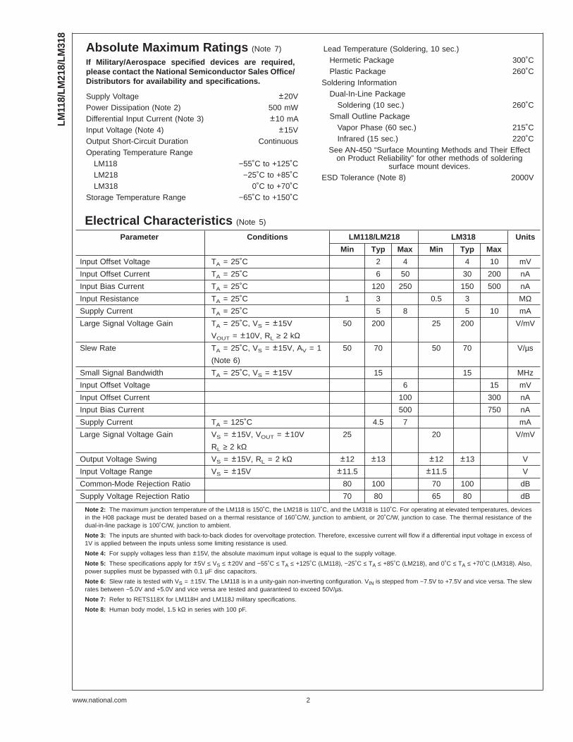
Absolute Maximum Ratings (Note 7)
If Military/Aerospace specified devices are required,please contact the National Semiconductor Sales Office/Distributors for availability and specifications.
Supply Voltage ±20VPower Dissipation (Note 2) 500 mWDifferential Input Current (Note 3) ±10 mAInput Voltage (Note 4) ±15VOutput Short-Circuit Duration ContinuousOperating Temperature Range
LM118 −55˚C to +125˚CLM218 −25˚C to +85˚CLM318 0˚C to +70˚C
Storage Temperature Range −65˚C to +150˚C
Lead Temperature (Soldering, 10 sec.)Hermetic Package 300˚CPlastic Package 260˚C
Soldering InformationDual-In-Line Package
Soldering (10 sec.) 260˚CSmall Outline Package
Vapor Phase (60 sec.) 215˚CInfrared (15 sec.) 220˚C
See AN-450 “Surface Mounting Methods and Their Effecton Product Reliability” for other methods of soldering
surface mount devices.ESD Tolerance (Note 8) 2000V
Electrical Characteristics (Note 5)
Parameter Conditions LM118/LM218 LM318 Units
Min Typ Max Min Typ Max
Input Offset Voltage TA = 25˚C 2 4 4 10 mV
Input Offset Current TA = 25˚C 6 50 30 200 nA
Input Bias Current TA = 25˚C 120 250 150 500 nA
Input Resistance TA = 25˚C 1 3 0.5 3 MΩSupply Current TA = 25˚C 5 8 5 10 mA
Large Signal Voltage Gain TA = 25˚C, VS = ±15V 50 200 25 200 V/mV
VOUT = ±10V, RL ≥ 2 kΩSlew Rate TA = 25˚C, VS = ±15V, AV = 1 50 70 50 70 V/µs
(Note 6)
Small Signal Bandwidth TA = 25˚C, VS = ±15V 15 15 MHz
Input Offset Voltage 6 15 mV
Input Offset Current 100 300 nA
Input Bias Current 500 750 nA
Supply Current TA = 125˚C 4.5 7 mA
Large Signal Voltage Gain VS = ±15V, VOUT = ±10V 25 20 V/mV
RL ≥ 2 kΩOutput Voltage Swing VS = ±15V, RL = 2 kΩ ±12 ±13 ±12 ±13 V
Input Voltage Range VS = ±15V ±11.5 ±11.5 V
Common-Mode Rejection Ratio 80 100 70 100 dB
Supply Voltage Rejection Ratio 70 80 65 80 dB
Note 2: The maximum junction temperature of the LM118 is 150˚C, the LM218 is 110˚C, and the LM318 is 110˚C. For operating at elevated temperatures, devicesin the H08 package must be derated based on a thermal resistance of 160˚C/W, junction to ambient, or 20˚C/W, junction to case. The thermal resistance of thedual-in-line package is 100˚C/W, junction to ambient.
Note 3: The inputs are shunted with back-to-back diodes for overvoltage protection. Therefore, excessive current will flow if a differential input voltage in excess of1V is applied between the inputs unless some limiting resistance is used.
Note 4: For supply voltages less than ±15V, the absolute maximum input voltage is equal to the supply voltage.
Note 5: These specifications apply for ±5V ≤ VS ≤ ±20V and −55˚C ≤ TA ≤ +125˚C (LM118), −25˚C ≤ TA ≤ +85˚C (LM218), and 0˚C ≤ TA ≤ +70˚C (LM318). Also,power supplies must be bypassed with 0.1 µF disc capacitors.
Note 6: Slew rate is tested with VS = ±15V. The LM118 is in a unity-gain non-inverting configuration. VIN is stepped from −7.5V to +7.5V and vice versa. The slewrates between −5.0V and +5.0V and vice versa are tested and guaranteed to exceed 50V/µs.
Note 7: Refer to RETS118X for LM118H and LM118J military specifications.
Note 8: Human body model, 1.5 kΩ in series with 100 pF.
LM11
8/LM
218/
LM31
8
www.national.com 2
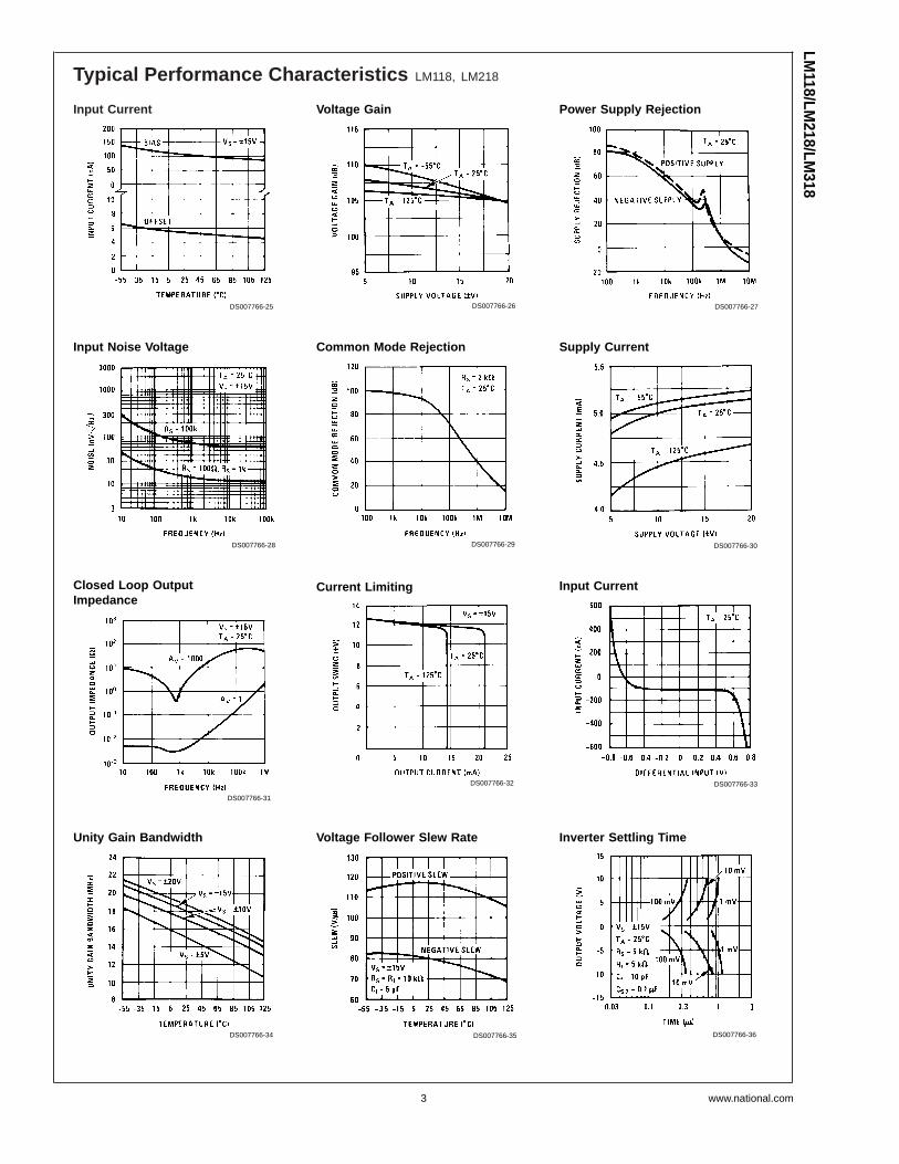
Typical Performance Characteristics LM118, LM218
Input Current
DS007766-25
Voltage Gain
DS007766-26
Power Supply Rejection
DS007766-27
Input Noise Voltage
DS007766-28
Common Mode Rejection
DS007766-29
Supply Current
DS007766-30
Closed Loop OutputImpedance
DS007766-31
Current Limiting
DS007766-32
Input Current
DS007766-33
Unity Gain Bandwidth
DS007766-34
Voltage Follower Slew Rate
DS007766-35
Inverter Settling Time
DS007766-36
LM118/LM
218/LM318
www.national.com3
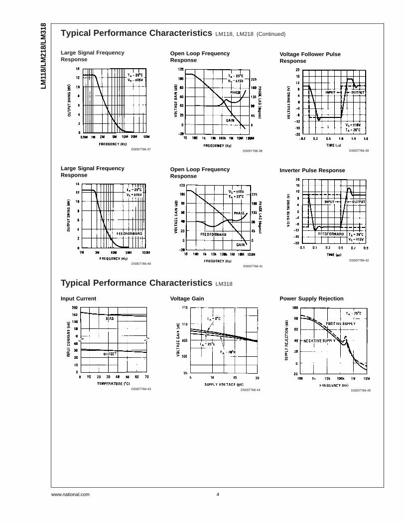
Typical Performance Characteristics LM118, LM218 (Continued)
Typical Performance Characteristics LM318
Large Signal FrequencyResponse
DS007766-37
Open Loop FrequencyResponse
DS007766-38
Voltage Follower PulseResponse
DS007766-39
Large Signal FrequencyResponse
DS007766-40
Open Loop FrequencyResponse
DS007766-41
Inverter Pulse Response
DS007766-42
Input Current
DS007766-43
Voltage Gain
DS007766-44
Power Supply Rejection
DS007766-45
LM11
8/LM
218/
LM31
8
www.national.com 4
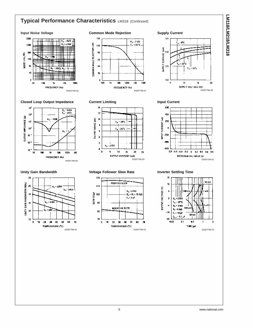
Typical Performance Characteristics LM318 (Continued)
Input Noise Voltage
DS007766-46
Common Mode Rejection
DS007766-47
Supply Current
DS007766-48
Closed Loop Output Impedance
DS007766-49
Current Limiting
DS007766-50
Input Current
DS007766-51
Unity Gain Bandwidth
DS007766-52
Voltage Follower Slew Rate
DS007766-53
Inverter Settling Time
DS007766-54
LM118/LM
218/LM318
www.national.com5
Typical Performance Characteristics LM318 (Continued)
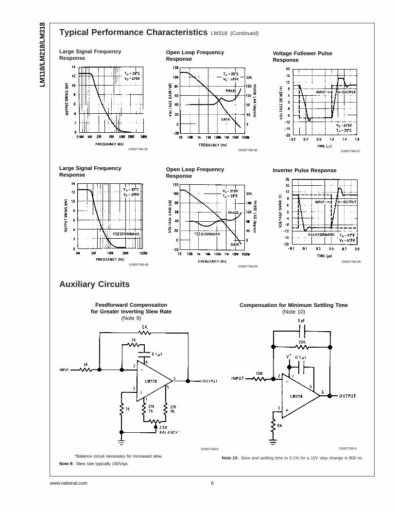
Auxiliary Circuits
Note 10: Slew and settling time to 0.1% for a 10V step change is 800 ns.
Large Signal FrequencyResponse
DS007766-55
Open Loop FrequencyResponse
DS007766-56
Voltage Follower PulseResponse
DS007766-57
Large Signal FrequencyResponse
DS007766-58
Open Loop FrequencyResponse
DS007766-59
Inverter Pulse Response
DS007766-60
Feedforward Compensationfor Greater Inverting Slew Rate
(Note 9)
DS007766-8
*Balance circuit necessary for increased slew.
Note 9: Slew rate typically 150V/µs.
Compensation for Minimum Settling Time(Note 10)
DS007766-9
LM11
8/LM
218/
LM31
8
www.national.com 6
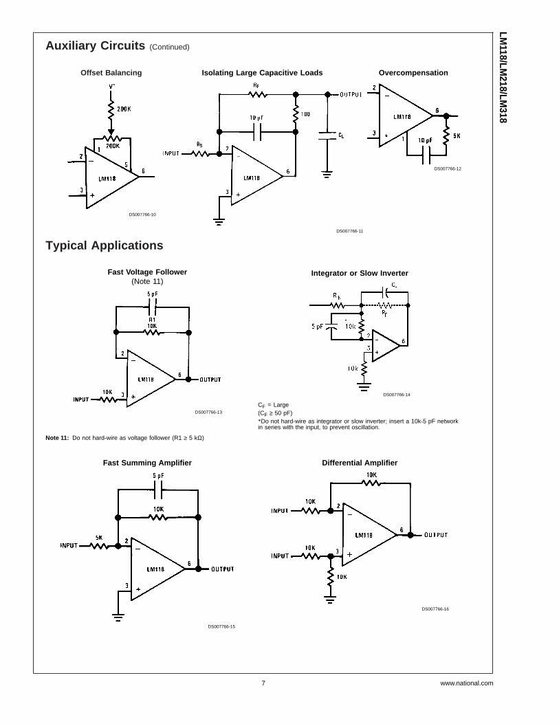
Auxiliary Circuits (Continued)
Typical Applications
Offset Balancing
DS007766-10
Isolating Large Capacitive Loads
DS007766-11
Overcompensation
DS007766-12
Fast Voltage Follower(Note 11)
DS007766-13
Integrator or Slow Inverter
DS007766-14
CF = Large(CF ≥ 50 pF)*Do not hard-wire as integrator or slow inverter; insert a 10k-5 pF networkin series with the input, to prevent oscillation.
Note 11: Do not hard-wire as voltage follower (R1 ≥ 5 kΩ)
Fast Summing Amplifier
DS007766-15
Differential Amplifier
DS007766-16
LM118/LM
218/LM318
www.national.com7
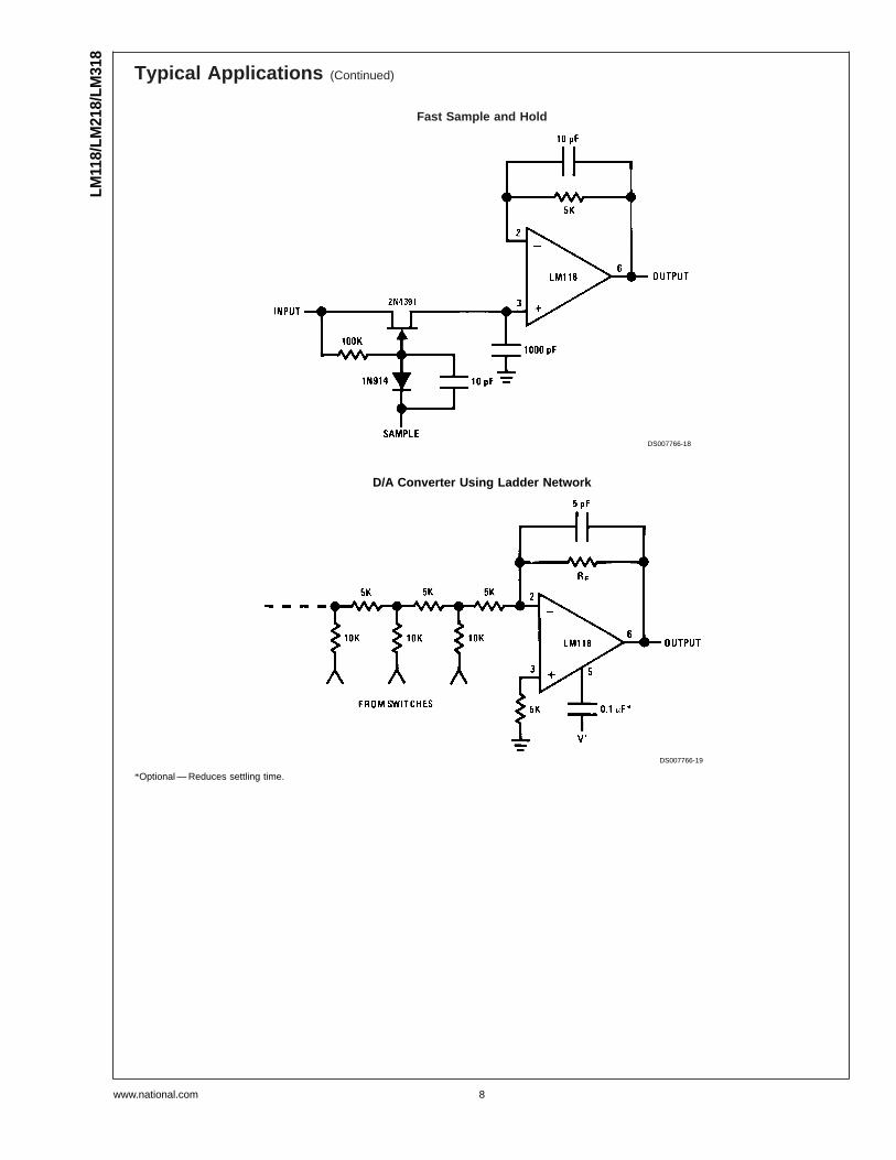
Typical Applications (Continued)
Fast Sample and Hold
DS007766-18
D/A Converter Using Ladder Network
DS007766-19
*Optional — Reduces settling time.
LM11
8/LM
218/
LM31
8
www.national.com 8
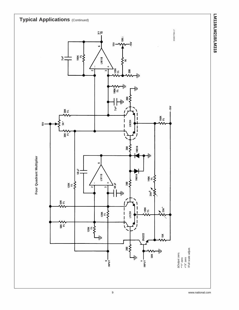
Typical Applications (Continued)
Fou
rQ
uadr
ant
Mul
tiplie
r
DS
0077
66-1
7
∆Out
put
zero
.* “
Y”
zero
+“X
”ze
ro‡ F
ulls
cale
adju
st.
LM118/LM
218/LM318
www.national.com9
Typical Applications (Continued)
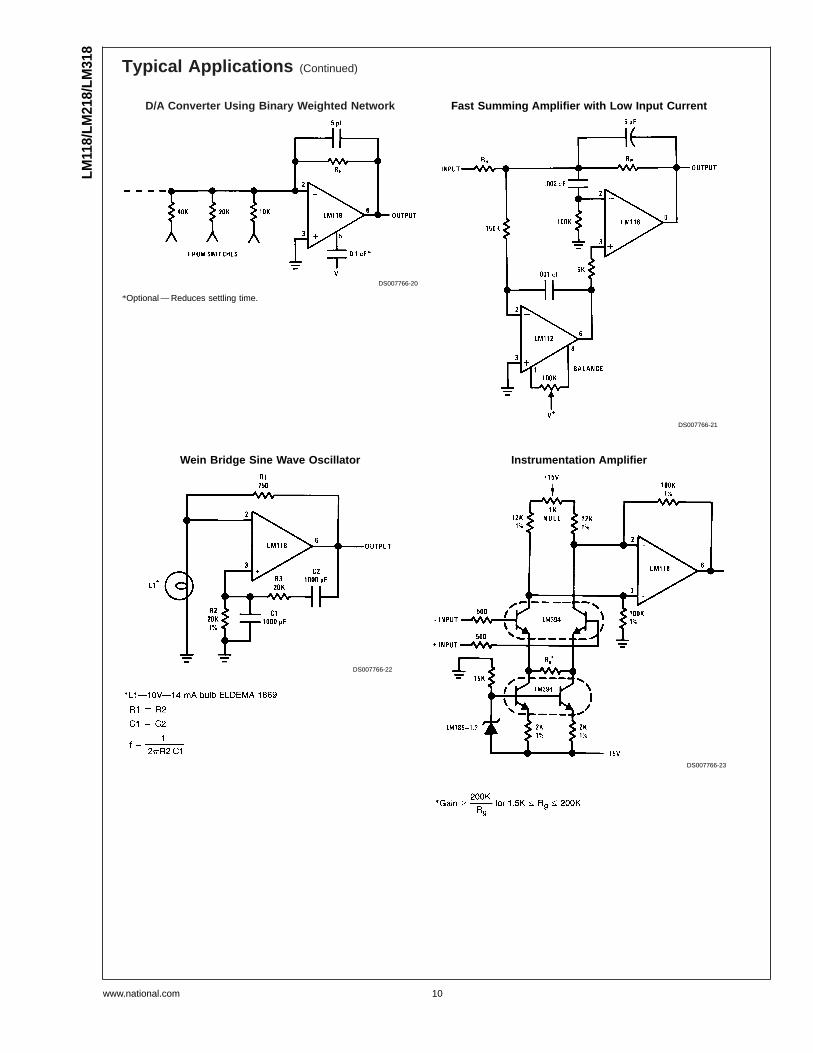
D/A Converter Using Binary Weighted Network
DS007766-20
*Optional — Reduces settling time.
Fast Summing Amplifier with Low Input Current
DS007766-21
Wein Bridge Sine Wave Oscillator
DS007766-22
Instrumentation Amplifier
DS007766-23
LM11
8/LM
218/
LM31
8
www.national.com 10
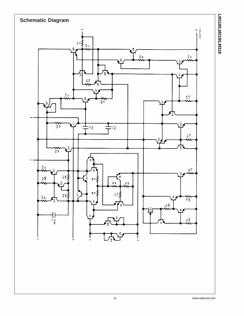
Schematic Diagram
DS
0077
66-1
LM118/LM
218/LM318
www.national.com11
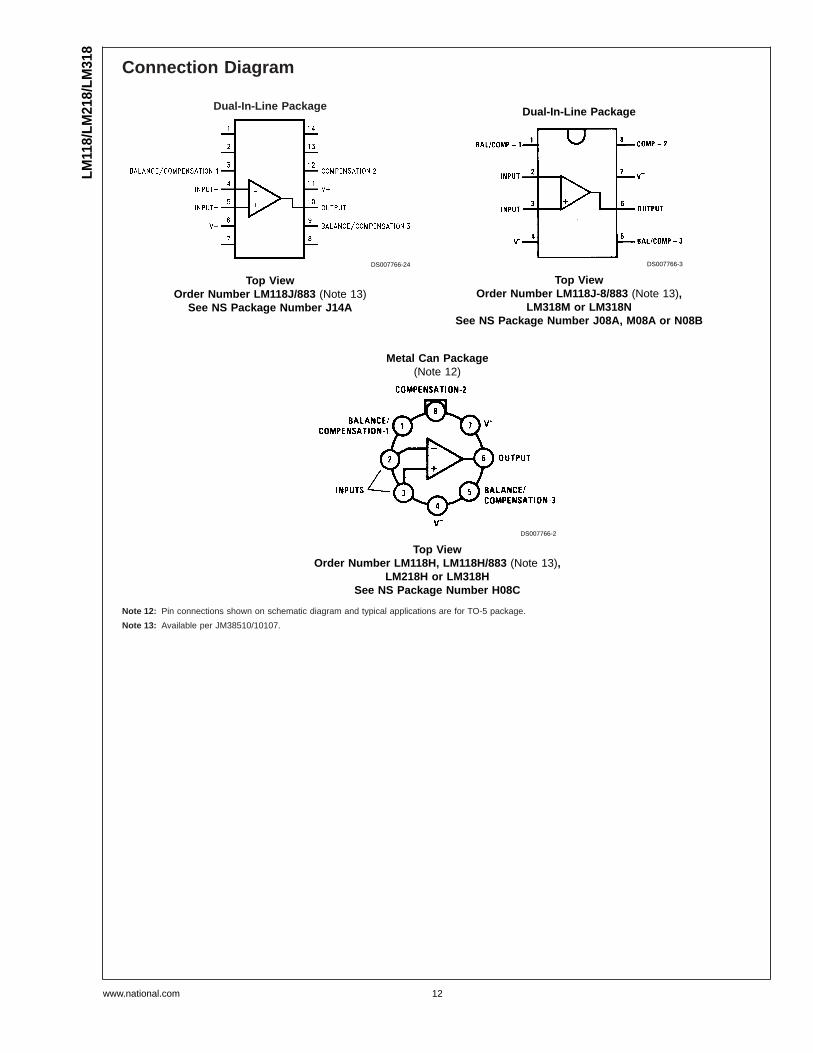
Connection Diagram
Note 12: Pin connections shown on schematic diagram and typical applications are for TO-5 package.
Note 13: Available per JM38510/10107.
Dual-In-Line Package
DS007766-24
Top ViewOrder Number LM118J/883 (Note 13)
See NS Package Number J14A
Dual-In-Line Package
DS007766-3
Top ViewOrder Number LM118J-8/883 (Note 13),
LM318M or LM318NSee NS Package Number J08A, M08A or N08B
Metal Can Package(Note 12)
DS007766-2
Top ViewOrder Number LM118H, LM118H/883 (Note 13),
LM218H or LM318HSee NS Package Number H08C
LM11
8/LM
218/
LM31
8
www.national.com 12
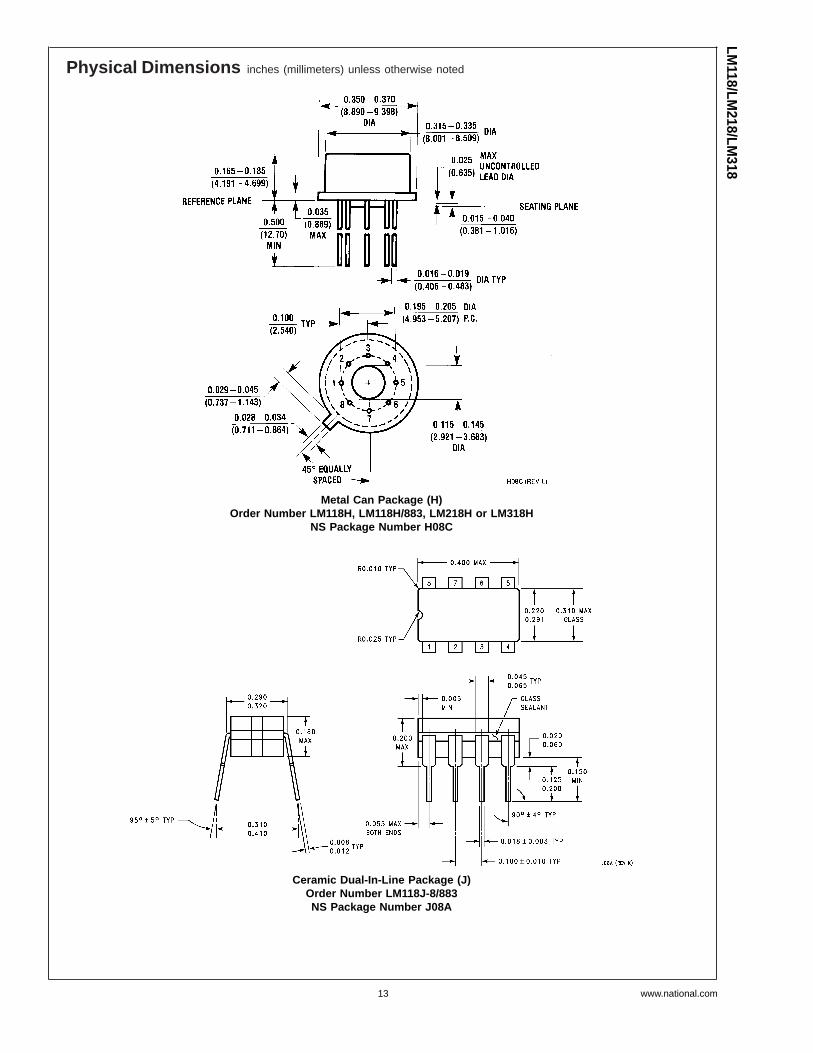
Physical Dimensions inches (millimeters) unless otherwise noted
Metal Can Package (H)Order Number LM118H, LM118H/883, LM218H or LM318H
NS Package Number H08C
Ceramic Dual-In-Line Package (J)Order Number LM118J-8/883NS Package Number J08A
LM118/LM
218/LM318
www.national.com13
Physical Dimensions inches (millimeters) unless otherwise noted (Continued)
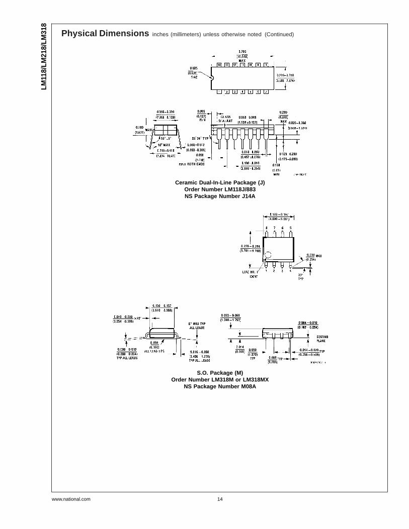
Ceramic Dual-In-Line Package (J)Order Number LM118J/883NS Package Number J14A
S.O. Package (M)Order Number LM318M or LM318MX
NS Package Number M08A
LM11
8/LM
218/
LM31
8
www.national.com 14
Physical Dimensions inches (millimeters) unless otherwise noted (Continued)
LIFE SUPPORT POLICY
NATIONAL’S PRODUCTS ARE NOT AUTHORIZED FOR USE AS CRITICAL COMPONENTS IN LIFE SUPPORTDEVICES OR SYSTEMS WITHOUT THE EXPRESS WRITTEN APPROVAL OF THE PRESIDENT AND GENERALCOUNSEL OF NATIONAL SEMICONDUCTOR CORPORATION. As used herein:
1. Life support devices or systems are devices orsystems which, (a) are intended for surgical implantinto the body, or (b) support or sustain life, andwhose failure to perform when properly used inaccordance with instructions for use provided in thelabeling, can be reasonably expected to result in asignificant injury to the user.
2. A critical component is any component of a lifesupport device or system whose failure to performcan be reasonably expected to cause the failure ofthe life support device or system, or to affect itssafety or effectiveness.
National SemiconductorCorporationAmericasTel: 1-800-272-9959Fax: 1-800-737-7018Email: [email protected]
National SemiconductorEurope
Fax: +49 (0) 180-530 85 86Email: [email protected]
Deutsch Tel: +49 (0) 69 9508 6208English Tel: +44 (0) 870 24 0 2171Français Tel: +33 (0) 1 41 91 87 90
National SemiconductorAsia Pacific CustomerResponse GroupTel: 65-2544466Fax: 65-2504466Email: [email protected]
National SemiconductorJapan Ltd.Tel: 81-3-5639-7560Email: [email protected]: 81-3-5639-7507
www.national.com
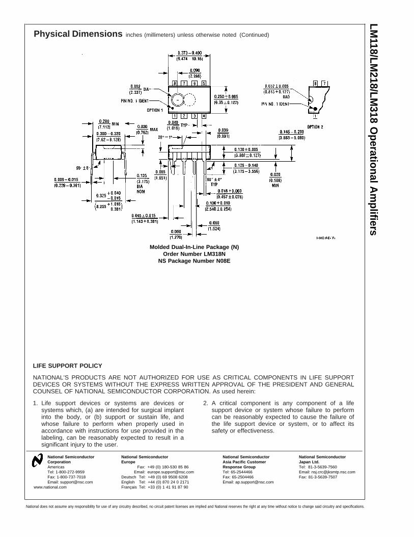
Molded Dual-In-Line Package (N)Order Number LM318N
NS Package Number N08E
LM118/LM
218/LM318
OperationalA
mplifiers
National does not assume any responsibility for use of any circuitry described, no circuit patent licenses are implied and National reserves the right at any time without notice to change said circuitry and specifications.
Recommended