Library Characterization and Static Timing Analysis
of Single-Track Circuits in GasP
by
Swetha Mettala Gilla
A thesis submitted in partial fulfillment of therequirements for the degree of
Master of Sciencein
Electrical and Computer Engineering
Thesis Committee:Xiaoyu Song, ChairDouglas V. HallChristof TeuscherMarly Roncken
Portland State Universityc!2010
Abstract
Library characterization and ‘Static Timing Analysis’ (STA) are widely used in the de-
sign of modern CMOS integrated circuits to confirm that critical timing constraints are
met. While many commercial tools are available to do timing validation using library
characterization and static timing analysis, their operation depends on calculations rela-
tive to a global synchronous clock. This thesis applies timing validation to circuits from
which the global synchronous clock is absent, making application of commercial tools
difficult. Previous work at the University of Southern California (USC) showed how
to overcome the incompatibility of commercial STA tools for asynchronous circuits.
This thesis shows how to overcome the incompatibility of library characterization for
asynchronous circuits, and ties the results to the STA solution of USC.
The particular family of circuits considered in this thesis is called GasP. GasP circuits
are light in area and power, and have demonstrated operation at about twice the through-
put one would expect from conventional clocked circuits. This makes GasP an ideal
candidate for modern network-on-chip and system-on-chip architectures. In part, GasP
circuits achieve their performance advantages by using a ‘single-track’ signaling proto-
col. Two GasP modules communicate with each other over a single wire. One module
drives the wire up and a second module at the other end of the wire drives the wire
down. This conflicts with the common assumption that wires are driven only from one
end. As a result, special circuitry is needed to characterize a GasP library module. This
thesis shows how to break a GasP module and its timing constraints into manageable
pieces and how to simulate and collect the data relevant for characterization and static
timing analysis. When combined with software tools for identifying the critical timing
constraints, these thesis results will provide confidence in the correct operation of GasP.
i

Acknowledgements
This work was partly sponsored under DARPA grant number HR0011-10-1-0069 for
“Fleet Studies”. In addition to DARPA, I would like to thank all the people who have
helped and inspired me during my thesis work.
I especially want to thank my advisor, Drs. Marly Roncken, for her guidance during
my research and study at Portland State University (PSU). Her perpetual energy and
enthusiasm in research were a great motivation to me. She was always accessible and
willing to help me with my research. She is the greatest personality I ever met in my 24
years life time. I admire her personality after Swami Vivekananda.
I was delighted to interact with Dr. Ivan Sutherland. It was a great opportunity to
participate in his seminars on GasP circuits, and an even greater opportunity to get the
chance to work with him on a timing flow for these circuits. His insight in asynchronous
circuit design is amazing. He explains anything that looks like “eschew obfuscation”
into something as obvious as “keep it simple”.0.1 To me, he defines what a world-class
researcher and teacher are about.
The GasP seminar class and my research with Marly and Ivan at the Asynchronous
Research Center (ARC) were both a turning point in my life and a wonderful experience.
The chance to publish and present my research work at the ASYNC 2010 conference0.1The text “eschew obfuscation” is on one of his sweatshirts.
ii

in Grenoble, France, broadened my view of the world, and enabled me to meet other
researchers and students working in the domain of asynchronous circuits.
I am much obliged to Professor Xiaoyu Song, for agreeing to be my thesis advisor. One
simply could not wish for a more friendly and understanding advisor. I feel blessed by
his encouragement to pursue this thesis topic, and to help me plan it. Professor Douglas
V. Hall, and Professor Christof Teuscher deserve special thanks as my thesis committee
members. I sincerely appreciate their participation and technical feedback.
I want to thank Prasad Joshi, Mallika Prakash, and Professor Peter Beerel from the
University of Southern California (USC), for making their static timing analysis flow
available, and for sending me their publications and any scripts they could officially
provide. The USC flow became the basis for my thesis. I am particularly grateful
to Prasad for being so patient in replying to my string of emails with questions, even
during the busy time before his wedding.
I would also like to thank my first manager at PSU, Lisa Weldon, for her support in
providing me with a student job during my initial struggling days at PSU when finances
were tight. My one year stint at HAL India opened my mind and motivated me to attend
graduate school. I would like to thank the friends from my college years in India, in
particular my badminton friends “6STARS”, and my close friend in Portland: Laddu.
My deepest gratitude goes to my family for their unflagging love and support. Without
them, this thesis would simply not exist. I am indebted to my mother, Indira Bai, for her
care and love. She is simply perfect. I have no suitable words to describe her everlasting
love to me. I remember her support when I encountered difficulties, and I am daily
reminded of her delicious dishes now that I do my own cooking. I thank my father,
Gopal Reddy, for believing in me and for supporting my study and career decisions.
iii
Contents
Abstract i
Acknowledgements ii
List of Figures xi
1 INTRODUCTION 1
1.1 GasP Circuits . . . . . . . . . . . . . . . . . . . . . . . . . . . . . . . 2
1.2 Timing Validation Flow . . . . . . . . . . . . . . . . . . . . . . . . . . 4
1.3 Reading Guide . . . . . . . . . . . . . . . . . . . . . . . . . . . . . . 6
2 6-4 GASP AND ITS RELATIVE TIMING CONSTRAINTS 10
3 LIBRARY CHARACTERIZATION PART-A: LOOK UP TABLES (LUTs) 14
3.1 Introduction . . . . . . . . . . . . . . . . . . . . . . . . . . . . . . . . 14
3.2 Step 1: Use Electric to Access the GasP Design . . . . . . . . . . . . . 18
3.3 Step 2: Create a Simulation Environment for the Design . . . . . . . . 20
3.4 Step 3: Generate Input Files for SPICE . . . . . . . . . . . . . . . . . . 21
iv
3.4.1 Generate a SPICE Netlist . . . . . . . . . . . . . . . . . . . . . 21
3.4.2 Generate SPICE Simulation Files: HEADER and TRAILER . . 21
3.5 Step 4: Modify the SPICE Input Files . . . . . . . . . . . . . . . . . . 23
3.5.1 Create Sweep Parameters in the SPICE Netlist . . . . . . . . . 23
3.5.2 Add Sweep and Measurement Statements to the TRAILER File 25
3.6 Step 5: Generate a SPICE Output File with Look Up Tables . . . . . . . 26
3.7 Validation . . . . . . . . . . . . . . . . . . . . . . . . . . . . . . . . . 30
3.8 Conclusion and Future Work for Chapter 3 . . . . . . . . . . . . . . . 33
4 LIBRARY CHARACTERIZATION PART-B: FROM GASP TO LUTs 34
4.1 Introduction . . . . . . . . . . . . . . . . . . . . . . . . . . . . . . . . 34
4.2 Quick Reminder: What’s a Look Up Table and How’s It Used? . . . . . 37
4.3 STEP 1: Partitioning Complex Paths into Simple Paths . . . . . . . . . 37
4.4 STEP 2: Defining an Accurate Simulation Set-Up for Simple Paths . . . 47
4.4.1 Circuit Partitioning for RT1 to RT4 . . . . . . . . . . . . . . . 47
4.4.2 Circuit Enhancements for Min-Max and Repetitive Simulations 55
4.4.2.1 Simulating Minimum Gate Delays . . . . . . . . . . 56
4.4.2.2 Autonomously Re-Initializing Un-Driven Wires . . . 59
4.4.2.3 Summary of Circuit Enhancements . . . . . . . . . . 64
4.4.3 Back to PART-A to Generate Look Up Tables . . . . . . . . . . 65
4.4.3.1 Setup for Figure 4.8 and LUTblue:PREDi"FIREi" . 66
v
4.4.3.2 Setup for Figure 4.9 and LUTblue:SUCCi+FIREi" . 68
4.4.3.3 Setup for Figure 4.7(b) and LUTblue:FIREi"Douti+ 69
4.4.3.4 Setup for Figure 4.10, LUTred/blue:FIREi+SUCCi+ 71
4.4.3.5 Setup for Figure 4.11, LUTblue/green:FIREi+PREDi" 76
4.5 General Simulation Setup Covering All Possible Sweep Cases . . . . . 81
4.5.1 Covering All Possible External Input Drives . . . . . . . . . . . 81
4.5.2 Covering Zero Exernal Output Loads . . . . . . . . . . . . . . 83
4.6 Conclusion and Future Work for Chapter 4 . . . . . . . . . . . . . . . 85
5 STATIC TIMING ANALYSIS OF 6-4 GASP USING LOOK UP TABLES 88
5.1 Introduction . . . . . . . . . . . . . . . . . . . . . . . . . . . . . . . . 89
5.2 STEP 1: From SPICED to PrimeTime Look Up Tables . . . . . . . . . 91
5.2.1 From Input Driver Size to Input Transition Slope . . . . . . . . 93
5.2.2 From Output Load Size to Output Load Capacitance . . . . . . 94
5.2.3 A Quick Sanity Check of the PrimeTime Look Up Tables . . . . 103
5.3 STEP 2: From 6-4 GasP Module to PrimeTime Black Box . . . . . . . 105
5.4 STEP 3: Create a Library File with SPICED Look Up Tables . . . . . . 106
5.4.1 STEP 3.1: Rename Look Up Tables to Match Black Box Names 107
5.4.2 STEP 3.2: Create a Library File with SPICED Look Up Tables . 110
5.5 STEP 4: Create Commands for Relative Timing Validation . . . . . . . 112
5.6 STEP 5: Run and Inspect Timing Reports . . . . . . . . . . . . . . . . 113
vi
5.7 Conclusion and Future Work for Chapter 5 . . . . . . . . . . . . . . . 116
6 SUMMARY AND DISCUSSION OF TIMING RESULTS 118
7 COMPARISON TO RELATED WORK 123
8 CONCLUSION AND FUTURE WORK 126
References 127
Appendices
A SPICE FILES FOR SPICE SWEEPS 132
A.1 SPICE Netlist Generated by Electric . . . . . . . . . . . . . . . . . . . 132
A.2 SPICE Simulation Set-Up File: HEADER . . . . . . . . . . . . . . . . 136
A.3 SPICE Simulation Set-Up File: TRAILER . . . . . . . . . . . . . . . . 136
A.4 Modified SPICE Netlist, Ready for Sweep . . . . . . . . . . . . . . . . 137
A.5 Modified SPICE TRAILER File, Ready for Sweep . . . . . . . . . . . 140
A.6 SPICE Output File . . . . . . . . . . . . . . . . . . . . . . . . . . . . 141
B SPICE FILES FOR SWEEPS IN THE DESIGN SPACE 142
B.1 SPICE Netlist for Reference Design . . . . . . . . . . . . . . . . . . . 142
B.2 SPICE TRAILER File for Reference Design . . . . . . . . . . . . . . . 151
B.3 SPICE Output File for Reference Design . . . . . . . . . . . . . . . . . 153
vii
C SPICE FILES FOR FIGURE 4.8 AND LUTblue:PREDi"FIREi" 154
C.1 SPICE Netlist . . . . . . . . . . . . . . . . . . . . . . . . . . . . . . . 154
C.2 SPICE Simulation Setup File: HEADER . . . . . . . . . . . . . . . . . 160
C.3 SPICE Simulation Setup File: TRAILER . . . . . . . . . . . . . . . . 161
C.4 SPICE Output File . . . . . . . . . . . . . . . . . . . . . . . . . . . . 163
D SPICE FILES FOR FIGURE 4.9 AND LUTblue:SUCCi+FIREi" 165
D.1 SPICE Netlist . . . . . . . . . . . . . . . . . . . . . . . . . . . . . . . 165
D.2 SPICE Simulation Setup File: HEADER . . . . . . . . . . . . . . . . . 171
D.3 SPICE Simulation Setup File: TRAILER . . . . . . . . . . . . . . . . 172
D.4 SPICE Output File . . . . . . . . . . . . . . . . . . . . . . . . . . . . 174
E SPICE FILES FOR FIGURE 4.7(b) AND LUTblue:FIREi"Douti+ 176
E.1 SPICE Netlist . . . . . . . . . . . . . . . . . . . . . . . . . . . . . . . 176
E.2 SPICE Simulation Setup File: HEADER . . . . . . . . . . . . . . . . . 180
E.3 SPICE Simulation Setup File: TRAILER . . . . . . . . . . . . . . . . 181
E.4 SPICE Output File . . . . . . . . . . . . . . . . . . . . . . . . . . . . 182
F SPICE FILES FOR FIGURE 4.10 AND LUTred/blue:FIREi+SUCCi+ 183
F.1 SPICE Netlist . . . . . . . . . . . . . . . . . . . . . . . . . . . . . . . 183
F.2 SPICE Simulation Setup File: HEADER . . . . . . . . . . . . . . . . . 189
F.3 SPICE Simulation Setup File: TRAILER . . . . . . . . . . . . . . . . 190
F.4 SPICE Output File . . . . . . . . . . . . . . . . . . . . . . . . . . . . 192
viii
G SPICE FILES FOR FIGURE 4.11 AND LUTblue/green:FIREi+PREDi" 194
G.1 SPICE Netlist . . . . . . . . . . . . . . . . . . . . . . . . . . . . . . . 194
G.2 SPICE Simulation Setup File: HEADER . . . . . . . . . . . . . . . . . 199
G.3 SPICE Simulation Setup File: TRAILER . . . . . . . . . . . . . . . . 200
G.4 SPICE Output File . . . . . . . . . . . . . . . . . . . . . . . . . . . . 202
H SPICE FILES FOR FIGURE 4.22 WITH ZERO EXTERNAL LOADS 204
H.1 SPICE Netlist . . . . . . . . . . . . . . . . . . . . . . . . . . . . . . . 204
H.2 SPICE Simulation Setup File: HEADER . . . . . . . . . . . . . . . . . 214
H.3 SPICE Simulation Setup File: TRAILER . . . . . . . . . . . . . . . . 215
H.4 SPICE Output File . . . . . . . . . . . . . . . . . . . . . . . . . . . . 217
I TRANSLATING LOAD SIZE INTO LOAD CAPACITANCE 219
I.1 SPICE Netlist . . . . . . . . . . . . . . . . . . . . . . . . . . . . . . . 219
I.2 SPICE Simulation File: HEADER . . . . . . . . . . . . . . . . . . . . 223
I.3 SPICE Simulation File: TRAILER . . . . . . . . . . . . . . . . . . . . 224
I.4 SPICE Output File . . . . . . . . . . . . . . . . . . . . . . . . . . . . 226
J PRIMETIME NETLIST FOR THE TWO-STAGE GASP FIFO 228
K PRIMETIME LIBRARYWITH SPICED LOOK UP TABLES 229
L PRIMETIME COMMANDS FOR VALIDATING RT1 TO RT4 234
ix
M PRIMETIME TIMING REPORTS 236
M.1 Timing Report for RT1 or RT(L2)TrfF!RstB . . . . . . . . . . . . . . . . 237
M.2 Timing Report for RT2 or RT(L2)TrfF!RstF . . . . . . . . . . . . . . . . 238
M.3 Timing Report for RT3 or RT(L2)TrfB!RstF . . . . . . . . . . . . . . . . 239
M.4 Timing Report for RT4 or RT(L2)TrfB!RstB . . . . . . . . . . . . . . . 240
N BONUS MATERIAL: DISTANCE CONSTRAINT GRAPH 241
O BONUS MATERIAL: SHORT-TO-MEDIUM-TO-LONGWIRE STUDY 253
P BONUS MATERIAL: THESIS POWERPOINT PRESENTATION 265
x
List of Figures
1.1 High-level view of a linear pipeline in GasP with a bundled datapath . . 4
1.2 Timing validation flow for GasP circuits . . . . . . . . . . . . . . . . . 5
2.1 Two-stage FIFO with two 6-4 GasP modules . . . . . . . . . . . . . . . 11
2.2 Relative timing constraints on single-track wire L2 of Figure 2.1 . . . . 13
3.1 Half-way GasP circuit . . . . . . . . . . . . . . . . . . . . . . . . . . . 19
3.2 Simulation environment for the Half-way GasP circuit in Figure 3.1 . . 19
3.3 Initial SPICE netlist with wrong null values for sweep size parameters . 22
3.4 SPICE netlist with corrected sweep size parameters . . . . . . . . . . . 24
3.5 SPICE simulation file fragment with sweep and measurement statements 27
3.6 SPICE output file fragment with look up table data . . . . . . . . . . . 29
3.7 Design sweep of the the Half-way GasP circuit in Figure 3.1 . . . . . . 31
3.8 Comparison of Design sweep versus SPICE sweep results . . . . . . . . 32
4.1 Wide-range look up table with delay and output slopes . . . . . . . . . 38
4.2 Wide-range landscape graphs with delay and output slope information . 38
4.3 Partitioning of the complex paths in relative timing constraint RT1 . . . 42
xi
4.4 Partitioning of the complex paths in relative timing constraint RT2 . . . 43
4.5 Partitioning of the complex paths in relative timing constraint RT3 . . . 44
4.6 Partitioning of the complex paths in relative timing constraint RT4 . . . 45
4.7 6-4 GasP circuit partitioning for RT1 to RT4 . . . . . . . . . . . . . . . 51
4.8 Circuit enhancement for LUTblue:PREDi"FIREi" for minimum delay 57
4.9 Circuit enhancement for LUTblue:SUCCi+FIREi" for minimum delay 58
4.10 Circuit enhancement LUTred/blue:FIREi+SUCCi+ to self-reset output 61
4.11 Circuit enhancement LUTblue/green:FIREi+PREDi" to self-reset output 63
4.12 Simulation setup for Figure 4.8 and LUTblue:PREDi"FIREi" . . . . . 67
4.13 Simulation setup for Figure 4.9 and LUTblue:SUCCi+FIREi" . . . . . 69
4.14 Simulation setup for Figure 4.7(b)and LUTblue:FIREi"Douti+ . . . . 70
4.15 Simulation setup for Figure 4.10 and LUTred/blue:FIREi+SUCCi+ . . 72
4.16 VCCS validation-1 for Figure 4.15 and LUTred/blue:FIREi+SUCCi+ . 74
4.17 VCCS validation-2 for Figure 4.15 and LUTred/blue:FIREi+SUCCi+ . 75
4.18 Simulation setup for Figure 4.11 and LUTblue/green:FIREi+PREDi" . 77
4.19 VCCS validation-1 for Figure 4.18 and LUTblue/green:FIREi+PREDi" 79
4.20 VCCS validation-2 for Figure 4.18 and LUTblue/green:FIREi+PREDi" 80
4.21 General simulation setup for look up table sweeps . . . . . . . . . . . . 82
4.22 Simulation setup for zero external ouput load . . . . . . . . . . . . . . 84
5.1 Simulation setup for translating load size into load capacitance . . . . . 95
xii
5.2 Graph showing the translation of load size into load capacitance . . . . 97
5.3 SPICE to PrimeTime look up table for LUTblue:PREDi"FIREi" . . . 98
5.4 SPICE to PrimeTime look up table for LUTblue:SUCCi+FIREi" . . . 99
5.5 SPICE to PrimeTime look up table for LUTblue:FIREi"Douti+ . . . . 100
5.6 SPICE to PrimeTime look up table for LUTred/blue:FIREi+SUCCi+ . 101
5.7 SPICE to PrimeTime look up table for LUTblue/green:FIREi+PREDi" 102
5.8 Landscape graphs with delay and output slope information . . . . . . . 103
5.9 Landscape graphs with delay and output slope information — continued 104
5.10 Split pin architecture of a basic 6-4 GasP module with its black box icon 105
5.11 Split pin architecture of the two-stage GasP FIFO . . . . . . . . . . . . 106
5.12 PrimeTime version of the relative timing constraints from Figure 2.2 . . 108
5.13 Renaming of SPICE look up table names into PrimeTime names . . . . 110
6.1 Rising and falling delays at the near and far end of single-track wire L2 120
6.2 Distance Constraint Graph for 6-4 GasP in 90nm CMOS . . . . . . . . 122
xiii
Chapter 1
INTRODUCTION
Concurrency and energy efficiency have taken their place as first class criteria in the
design of modern circuits and systems along with, and at times even at the cost of,
speed in terms of throughput and latency. The design of modern concurrent systems
centers around a communication infrastructure that connects a number of functional
blocks. Examples are IBM Research’s Cell systems [8], Intel’s research milestones for
many-core and teraflop systems [9, 10], and Sun’s (now: Oracle’s) UltraSPARC T1
microprocessor, codenamed ‘Niagara’ [11]. Each block tends to have its own clock or
timing regime, fit to best match its operations. From a timing point of view, the blocks
operate asynchronously. Even if blocks use the same clock frequency, their operations
are likely to be skewed or out of phase with respect to each other.
The Asynchronous Research Center (ARC) at Portland State University is building a
concurrent system architecture called ‘Fleet’ [31, 13] centered around an asynchronous
communication network, built using GasP modules. Fleet anticipates the use of a va-
riety of computation blocks of low to modest complexity, called ‘ships’, such as low-
power adders and multipliers, high-speed adders and multipliers, dividers, various shift
and sort functions, I/O functions, and memory blocks. The ships can be synchronous
1
or asynchronous, including GasP. They can be integrated in a single chip, or spread
over different chips or FPGAs. This makes it possible to import asynchronous ships
designed by companies like Achronix Semiconductor Corporation [5] for asynchronous
FPGA’s, FulcrumMicrosystems [7] for high-density ethernet switches, and Tiempo [14]
for ultra-low-power functions. Alternatively, Fleet can take ships built using differ-
ent asynchronous design styles from other academic and research institutes. For an
overview of asynchronous design styles and a list of institutes that study and develop
asynchronous circuits, see the yearly international symposium on asynchronous circuits
and systems, which is approaching its 17-th anniversary [12].
1.1 GasP Circuits
The target circuits for this thesis are GasP circuits. These circuits use handshake signal-
ing over a single-track wire and single-rail data encoding. This results in (N+1) wires to
communicate N data bits. The combination of single-track handshaking and single-rail
data results in light-weight circuits — light in area and light in power. GasP circuits
also happen to be about twice as fast as one would expect of a globally clocked circuit
implemented in the same technology. Add the flexibility and elasticity of asynchronous
design to high speed, low power, and low area, and you get an excellent circuit family
for on-chip communication — which is why Fleet uses a GasP network on chip.
In addition to the data wires, GasP circuits use a single wire for timing. The single-track
handshake is a bi-directional communication on that wire. A logical high voltage level
on the wire indicates a request, and a logical low voltage level on the wire indicates an
acknowledge signal. The wire has two drivers— one at each end, one for the request and
one for the acknowledge. This leads naturally to a two-phase return-to-zero handshake.
2
The wire is shared, so each end drives only briefly. The brief drive avoids a drive fight
between the two ends. In addition, each driver responds only to changes at its own end.
It’s this local response that enables the communication to complete in two phases. To
make this work, we need some faith: faith in our own engineering and in the design
tools that we use. The faith in a single-track handshake depends on two assumptions:
Assumption 1: The brief drive is long enough to traverse the wire.
Assumption 2: The voltage level at the near end of the wire reflects the far-end level.
Data in GasP are exchanged using a bundled-data, also known as single-rail, protocol.
Data bits are represented using one wire per bit, just like in conventional synchronous
circuits. The single-track request signal indicates that the sender module has new data
for the receiver module, i.e. it acts as a ‘data valid’ signal for the data transfer. The
single-track acknowledge signal indicates that the receiver module has finished consum-
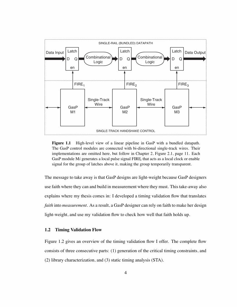
ing the data, i.e. it acts as a ‘completion’ signal for the data transfer. Figure 1.1 gives a
high-level overview of a linear pipeline in GasP. The GasP modules are connected with
single-track wires. Each GasP module Mi generates a local pulse signal FIREi that acts
as a local clock or enable signal for the group of latches above it, making the group tem-
porarily transparent. To make this work, we need — again — some faith. The faith in
a bundled datapath operation can be expressed in terms of conventional setup and hold
times between the data inputs and outputs and the clock enable signals at both ends of
the datapath. The data bundling constraints in GasP and their static timing analysis have
been solved successfully by Prasad Joshi in his Master of Science thesis [2].
In the rest of my thesis, I will assume that timing constraints related to datapaths are no
longer an issue, and I will henceforth ignore the datapath portion of a GasP design.
3
FIRE1 FIRE2 FIRE3
GasPM1
GasPM2
GasPM3
Latch
D Q
en
Latch
D Q
en
Latch
D Q
en
CombinationalLogic
CombinationalLogic
Single-TrackWire
Single-TrackWire
Data Input Data Output
SINGLE-RAIL (BUNDLED) DATAPATH
SINGLE-TRACK HANDSHAKE CONTROL
Figure 1.1 High-level view of a linear pipeline in GasP with a bundled datapath.The GasP control modules are connected with bi-directional single-track wires. Theirimplementations are omitted here, but follow in Chapter 2, Figure 2.1, page 11. EachGasP module Mi generates a local pulse signal FIREi that acts as a local clock or enablesignal for the group of latches above it, making the group temporarily transparent.
The message to take away is that GasP designs are light-weight because GasP designers
use faith where they can and build in measurement where they must. This take-away also
explains where my thesis comes in: I developed a timing validation flow that translates
faith intomeasurement. As a result, a GasP designer can rely on faith to make her design
light-weight, and use my validation flow to check how well that faith holds up.
1.2 Timing Validation Flow
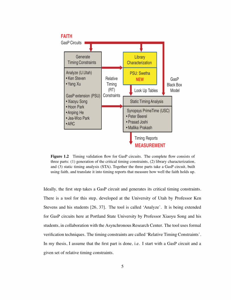
Figure 1.2 gives an overview of the timing validation flow I offer. The complete flow
consists of three consecutive parts: (1) generation of the critical timing constraints, and
(2) library characterization, and (3) static timing analysis (STA).
4
PSU: SwethaNEW
LibraryCharacterization
Look Up TablesGasP extension (PSU)
Analyze (U.Utah)• Ken Steven• Yang Xu
• Xiaoyu Song• Hoon Park • Anping He• Jea-Woo Park• ARC
Generate Timing Constraints
FAITH GasP Circuits
Relative Timing(RT)
Constraints
•••
Static Timing Analysis
Synopsys PrimeTime (USC) Peter Beerel Prasad JoshiMallika Prakash
GasP Black Box
Model
MEASUREMENTTiming Reports
Figure 1.2 Timing validation flow for GasP circuits. The complete flow consists ofthree parts: (1) generation of the critical timing constraints, (2) library characterization,and (3) static timing analysis (STA). Together the three parts take a GasP circuit, builtusing faith, and translate it into timing reports that measure how well the faith holds up.
Ideally, the first step takes a GasP circuit and generates its critical timing constraints.
There is a tool for this step, developed at the University of Utah by Professor Ken
Stevens and his students [26, 37]. The tool is called ‘Analyze’. It is being extended
for GasP circuits here at Portland State University by Professor Xiaoyu Song and his
students, in collaboration with the Asynchronous Research Center. The tool uses formal
verification techniques. The timing constraints are called ‘Relative Timing Constraints’.
In my thesis, I assume that the first part is done, i.e. I start with a GasP circuit and a
given set of relative timing constraints.
5
The second step in the flow, and the first step addressed in my thesis is called ‘Library
Characterization’. This is the key part of my thesis, and it’s new work. In this step, I
take a GasP circuit and its relative timing constraints. I partition these into manageable
pieces that I simulate for various operating conditions. And I generate a collection of
so-called ‘Look Up Tables’ (LUTs) that store the timing information of the paths under
those conditions.
I feed these look up tables and a so-called ‘Black Box’ model of the GasP circuit into
static timing analysis. The black box shows only the circuit input and output pins,
and hides the combinational loops and single-track details of GasP. This third step is not
new. The black box model and the analysis commands for the relative timing constraints
were developed at the University of Southern California by Professor Peter Beerel and
his students. The tool itself is a commercial tool by Synopsys called ‘PrimeTime’ [35].
All I had to do was to get it running at Portland State University and to import my timing
constraints and look up tables.
The result of static timing analysis is a collection of timing reports, one for each relative
timing constraint, showing how much slack there is to make or break the constraint.
So, in total, these three flow parts take a GasP circuit, built using faith, and translate it
into timing reports that measure how well the faith holds up. In summary: the timing
validation flow outlined in Figure 1.2 translates faith into measurement.1.1
1.3 Reading Guide
I have now told you why I built a timing validation flow for GasP, and which parts I
borrowed and which parts are new. The rest of my thesis is organized as follows:1.1Of course, the real measurement is the silicon, but that is a very expensive and time-consuming
measurement. The measurement I am talking about is a simulated measurement.
6
• Chapter 2 gives the design details on GasP, and identifies the four key relative
timing constraints for single-track communication. In this thesis, I work with
TSMC 90nm CMOS implementations of 6-4 GasP, but that’s just a choice. This
choice has zero impact on the generality and applicability of my flow to other
CMOS implementations or other members of the GasP family, such as 4-2 GasP
or 3-7 GasP. More GasP details can be found in Appendix O or [30, 29, 18, 13].
• Chapter 3–4 are about library characterization, and cover he biggest part of my
thesis. Here, I show how timing constraints are translated into look up tables.
This requires three steps. In the first step, I partition the timing constraints into
manageable pieces. In the second step, I build a simulation environment for
each partitioned timing constraint, using the schematic design environment pro-
vided by Electric [24] and the transistor-level simulation environment provided
by SPICE [34]. In the third step, I run the SPICE simulator to generate the look
up tables. Chapter 3 explains the basic simulation environment in Electric and
the SPICE commands for the third step. Chapter 4 takes a 6-4 GasP module and
the four key relative timing constraints identified in Chapter 2, and goes into the
details of each step.
• Chapter 5 shows how static timing analysis uses the timing information in the look
up tables to validate the four relative timing constraints. Here, I explain the STA
part of the flow and show how to import the look up tables generated in Chapter 4.
• Chapter 6 analyzes the timing results produced by the STA part of the flow. Be-
cause the proof of the pudding is in the eating, I did not just propose and develop
a timing validation flow, but I also used it. I used it to validate the four timing
constraints that are key to single-track handshake communication in 6-4 GasP.
7

Moreover, I show that the results in the timing reports are compatible with the
results of my ASYNC 2010 publication in [18] and Appendix O.
• Chapter 7 compares my approach to the approach taken by USC. I deliberately
postpone this comparison to the end of my thesis, because this enables me to give
a more in-depth explanation than would be possible with an up-front comparison
where the reader has not yet had a chance to read any of my work.
• Chapter 8 concludes this thesis and indicates what next steps are needed. As far as
future work goes, what this flow needs most is a wire delay model. The wire delay
model should distinguish the effective capacitance seen at the near end of the wire
from the capacitance and delay seen at the far end. It may be that an Elmore delay
model suffices [23, 36]. Last but not least: this flow needs automation so it can
become an integral part of the GasP design environment.
Chapters 2–7 are also available as internal reports [16, 17, 19] from the Asynchronous
Research Center at Portland State University, where I worked as a Research Assistant.
The reports are co-authored by Marly Roncken and Ivan Sutherland. For that reason,
Chapters 2–7 use as author identity ‘we’ instead of ‘I’. The author identity changes to
‘I’ again when I conclude this thesis in Chapter 8.
After working with flows that require various tools and translations from file formats
in one tool to file formats in another tool, I have come to realize that documentation
often lacks the clarity and teaching capability that it should provide. I have therefore
set an extra goal for my thesis. Not only do I want to show that I generated a timing
validation flow for single-track circuits in GasP, but I also want to explain this flow in a
way that is useful for professors as well as for their students. I have set up this thesis so
8
that others can easily use the flow, execute it, and validate its results. The many files in
Appendices A–M in this thesis are there to support this extra goal.
In addition to Appendices A–M with files, I have added three more Appendices N–P
with extra bonus material to complete the picture and provide a quick tour of this thesis:
• Appendix N contains the ARC report on the Distance Constraint Graph. I defined
this graph notion when studying 6-4 GasP with short wires. It has turned out to be
a useful abstraction for thinking about wire lengths and module distances versus
critical timing paths (or relative timing constraints as we call them at the ARC).
• Appendix O contains the paper that I presented and published at ASYNC 2010. It
contains the short-to-medium-to-long wire studies for 6-4 GasP. The above ARC
report and the ASYNC 2010 paper shaped the topic of this thesis. Both are cited
repeatedly in this thesis to motivate their inclusion. IEEE and my co-authors
graciously allowed me to include them as appendix to this thesis.
• Appendix P contains the handout of the powerpoint presentation that I presented
during my thesis defense, on 29 October 2010. Reading the powerpoint slides,
which I printed as a 4-slides-per-page handout may be the quickest way to get a
tour of this thesis. I hope you will enjoy the tour!
9

Chapter 2
6-4 GASP AND ITS RELATIVE TIMING CONSTRAINTS
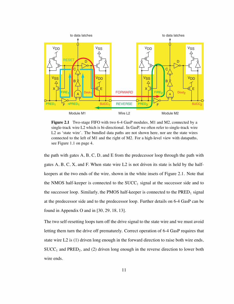
Chapter 2 introduces the basics of GasP circuits. We use a 6-4 GasP FIFO module as
reference design. Figure 2.1 shows a two-stage FIFO with two 6-4 GasP FIFO modules,
M1 and M2. Modules M1 and M2 are connected by a bi-directional wire L2 in the
middle. Module M1 drives wire L2 high via P-transistor E and module M2 drives wire
L2 low via N-transistor X. Wire L2 is called a ‘single-track wire’, but in GasP we also
call it a ‘state wire’ because it holds state. It is high when it has valid data in which case
we call its state ‘Full’ and it is low when it has a bubble, in which case we call its state
‘Empty’. GasP module M1 fires when its PRED1 signal is high, meaning full, and its
SUCC1 signal is low, meaning empty.
When M1 fires, it forwards the full state on its left to state wire L2 and module M2 on
its right, using the six gates on the red arrow in Figure 2.1: A, B, C, D, E and F. When
M2 fires it drains state wire L2, using the 4 gates on the green arrow: A, B, C and X.
The name for 6-4 GasP comes from the six gates in the path going forward from one
module to the next, and the four gates in the reverse path.
In addition, a 6-4 GasP module has two self-resetting loops of five gates each, as in-
dicated by the blue arrows in Figure 2.1. We distinguish the successor loop through
10
PRED1 SUCC1
A
B
F
D
C
EXDout1
VDDVSS
VSSVDD
FIRE1
PRED2 SUCC2
to data latches
A
B
F
D
C
EXDout2
VDDVSS
VSSVDD
FIRE2
single-trackstate wire
(high is FULL)
to data latches
nPRED1
RESET
FORWARD
REVERSE
Module M1 Wire L2 Module M2
Figure 2.1 Two-stage FIFO with two 6-4 GasP modules, M1 and M2, connected by asingle-track wire L2 which is bi-directional. In GasP, we often refer to single-track wireL2 as ‘state wire’. The bundled data paths are not shown here, nor are the state wiresconnected to the left of M1 and the right of M2. For a high-level view with datapaths,see Figure 1.1 on page 4.
the path with gates A, B, C, D, and E from the predecessor loop through the path with
gates A, B, C, X, and F. When state wire L2 is not driven its state is held by the half-
keepers at the two ends of the wire, shown in the white insets of Figure 2.1. Note that
the NMOS half-keeper is connected to the SUCC1 signal at the successor side and to
the successor loop. Similarly, the PMOS half-keeper is connected to the PRED1 signal
at the predecessor side and to the predecessor loop. Further details on 6-4 GasP can be
found in Appendix O and in [30, 29, 18, 13].
The two self-resetting loops turn off the drive signal to the state wire and we must avoid
letting them turn the drive off prematurely. Correct operation of 6-4 GasP requires that
state wire L2 is (1) driven long enough in the forward direction to raise both wire ends,
SUCC1 and PRED2, and (2) driven long enough in the reverse direction to lower both
wire ends.
11

To validate that both (1) and (2) hold, we compare the forward and the reverse drive
delays for L2 to the self-resetting loop delays and require the former to beat the latter.
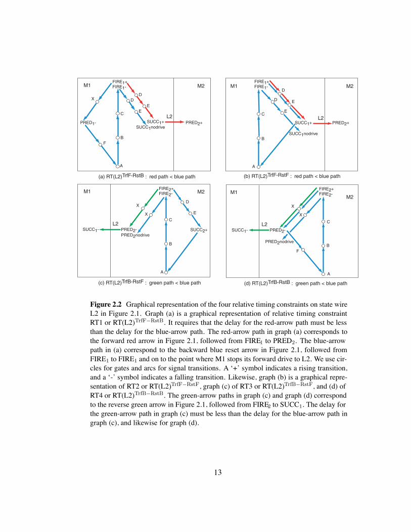
Thus, state wire L2 in Figure 2.1 produces the following four relative timing constraints:
• RT1 or RT(L2)TrfF!RstB : The forward transfer delay to drive both ends of L2 high
through DE in module M1 is shorter than the delay of the backward self-resetting
loop through XFABCDE in M1 that stops the drive. Figure 2.2(a) illustrates this
graphically: the red path must be shorter than the blue path.
• RT2 or RT(L2)TrfF!RstF : The forward transfer delay to drive both ends of L2 high
through DE in module M1 is shorter than the delay of the forward self-resetting
loop through DEABCDE in M1 that stops the drive. Figure 2.2(b) illustrates this
graphically: the red path must be shorter than the blue path.
• RT3 or RT(L2)TrfB!RstF : The reverse transfer delay to drive both ends of L2 low
through X in module M2 is shorter than the delay of the forward self-resetting
loop through DEABCX in M2 that stops the drive. Figure 2.2(c) illustrates this
graphically: the green path must be shorter than the blue path.
• RT4 or RT(L2)TrfB!RstB : The backward transfer delay to drive both L2 ends low
through X in module M2 is shorter than the delay of the backward self-resetting
loop through XFABCX in M2 that stops the drive. Figure 2.2(d) illustrates this
graphically: the green path must be shorter than the blue path.
From these relative timing constraints, and their graphical representations in Figure 2.2,
it follows that the red, green and blue paths in Figures 2.1–2.2 are the circuit paths
whose delays we must calculate. Note that the blue paths contain (combinational) loops.
This classifies them as complex paths, and as such as paths too difficult to handle by
commercial library characterization and static timing analysis tools. In Chapters 4 and
5 we explain how this can be solved.
12
PRED2-
PRED2nodrive
FIRE2+FIRE2-
A
B
C
X
SUCC1-
X
F
(d) RT(L2)TrfB-RstB : green path < blue path
L2
E
D
FIRE1+FIRE1-
SUCC1+
A
B
C
PRED2+
SUCC1nodrive
E
DM1 M2
(b) RT(L2)TrfF-RstF : red path < blue path
L2
A
B
C
FIRE2+FIRE2-
PRED2-PRED2nodrive
SUCC2+
X
E
D
SUCC1-
X
(c) RT(L2)TrfB-RstF : green path < blue path
L2
FIRE1+FIRE1-
PRED1- SUCC1+
A
B
C
X
F
E
D
E
D
SUCC1nodrivePRED2+
M1 M2
M1M2
M1 M2
(a) RT(L2)TrfF-RstB : red path < blue path
L2
Figure 2.2 Graphical representation of the four relative timing constraints on state wireL2 in Figure 2.1. Graph (a) is a graphical representation of relative timing constraintRT1 or RT(L2)TrfF!RstB. It requires that the delay for the red-arrow path must be lessthan the delay for the blue-arrow path. The red-arrow path in graph (a) corresponds tothe forward red arrow in Figure 2.1, followed from FIRE1 to PRED2. The blue-arrowpath in (a) correspond to the backward blue reset arrow in Figure 2.1, followed fromFIRE1 to FIRE1 and on to the point where M1 stops its forward drive to L2. We use cir-cles for gates and arcs for signal transitions. A ‘+’ symbol indicates a rising transition,and a ‘-’ symbol indicates a falling transition. Likewise, graph (b) is a graphical repre-sentation of RT2 or RT(L2)TrfF!RstF, graph (c) of RT3 or RT(L2)TrfB!RstF, and (d) ofRT4 or RT(L2)TrfB!RstB. The green-arrow paths in graph (c) and graph (d) correspondto the reverse green arrow in Figure 2.1, followed from FIRE2 to SUCC1. The delay forthe green-arrow path in graph (c) must be less than the delay for the blue-arrow path ingraph (c), and likewise for graph (d).
13
Chapter 3
LIBRARY CHARACTERIZATION PART-A: LOOK UP TABLES (LUTs)
Chapter 3 is also available as internal report ARC2010-smg01 [16]. It describes the
results of our investigations into creating look up tables that accurately characterize the
timing information of a 6-4 GasP module. These tables allow us to bypass tool issues
related to loops and other design elements used in asynchronous circuits that standard
tools for synchronous circuit designs are not accustomed to. In addition to avoiding tool
issues, the use of look up tables can also speed up the static timing analysis (STA) of a
large GasP design. We present our results in two parts. PART-A, described here, takes a
simple circuit without loops, and shows the basic flow aspects from the schematics entry
level of the design in Electric to the SPICE simulation set-up and the SPICE output files
with the look up tables. PART-B, described in Chapter 4 shows how to partition complex
circuits with loops and multiple inputs and outputs into designs simple enough for the
characterization flow in PART-A.
3.1 Introduction
A look up table is basically an array with a search key and a corresponding result. look
up tables are often used to reduce the run time of a computation. In the old days people
used printed look up tables like logarithmic or trigonometry tables to speed up hand
14
calculations. Look up tables are used in one of three ways: (1) Exact match or (2)
Interpolation, or (3) Extrapolation. When the search key exists, i.e. when it exactly
matches a look up table entry, we can simply read out the corresponding result value.
When the search key does not match any of the look up table entries, we estimate the
result value for a search key that is inside respectively outside the entry range, by using
interpolation respectively extrapolation techniques on the result values of the look up
table entries that are closest in value to the search key. For our usage, linear interpolation
and extrapolation techniques suffice.
We use look up tables (LUTs) for static timing analysis (STA) of GasP circuits. The look
up tables that we generate store the path delays for a GasP circuit, under various oper-
ating conditions. Our look up tables use a two-dimensional search key (wid1 # wid2)
and store three types of delay:
1. (wid1 # wid2)$ slope (in[1])
2. (wid1 # wid2)$ delay (in[1] to out[1])
3. (wid1 # wid2)$ slope (out[1])
where:
• wid1 is the size of the external gate driving path input in[1].
• wid2 is the size of the external gate driven by path output out[1].
• slope(in[1]) is the input transition slope, a.k.a. input slew time, as denoted by the
time difference (tin2"tin1) from time tin1 when a rising input transition on in[1]
passes the 20% supply voltage point to time tin2 when it passes the 80% voltage
point — and vice versa for a falling input transition.
• delay(in[1] to out[1]) is the input-to-output transition delay time (tout"tin) from
time tin when the input transition on in[1] passes the 50% supply voltage point to
time tout when the output transition on out[1] passes the 50% supply point.
15
• slope(out[1]) is the output transition slope, a.k.a. output slew, as for instance
denoted by the time difference (tout2 " tout1) from time tout1 when a falling
output transition on out[1] passes the 80% supply voltage point to time tout2
when it passes the 20% point — and vice versa for a rising output transition.
For those of you who are familiar with standard static timing analysis (STA) tools like
PrimeTime of Synopsys: note that the search keys in our look up tables are different.
We use sizing information instead of input slopes and output loads. By doing this we
can use the theory of Logical Effort [32] in both the design and the characterization of
our circuits. We feel that this makes the characterization process less artificial and more
realistic. To accommodate standard STA tools, we measure the input slopes for a given
drive size and we have methods to translate a driven output size into an output load
which we’ll explain in Chapter 5. In the present Chapter 3, we show how to generate
such look up tables for simple paths in a GasP circuit, i.e. paths with one input and one
output, and without feedback. Complex paths are the topic of Chapter 4.
There are basically two ways to sweep the search key values for (wid1 # wid2) and
generate the resulting delay and slope information for a simple path in a GasP circuit.
One approach is to design all sweeps in parallel at the schematic entry level and create
one composite SPICE run. This works provided the size of the simulation result file is
small enough to be read back into Electric’s schematic entry and layout environment [24]
for validation and debug. We had some trouble with this in our long wire studies for [18].
We will investigate another approach where we design exactly one parameterized sweep
schematics in Electric, which we will simulate multiple times, each time with a new set
of parameter values, using the .DATA sweep command in SPICE [34].
16
Our look up table generation procedure distinguishes the following five steps:
Step 1: Use schematics and layout tool Electric to access the GasP design.
Step 2: In Electric, create a realistic simulation environment for the GasP design.
Step 3: From Electric, generate input files for SPICE:
• Generate a SPICE netlist for the GasP design and its environment.
• Generate SPICE simulation set-up files.
Step 4: Modify the SPICE input files:
• In the netlist, create sweep parameters for wid1 and wid2.
• In the simulation set-up files, add sweep statements for wid1 and wid2, and
measurement statements for in[1] and out[1].
Step 5: Run SPICE and capture the look up table results in an output file.
The outline for the rest of Chapter 3 is as follows. Sections 3.2 to 3.6 each discuss one
step in our 5-step look up table generation procedure. We use the 6-4 GasP circuit of
Figure 3.1 on page 19 as our baseline example. Section 3.7 compares the results ob-
tained by applying the 5-step procedure to this circuit to the results obtained from the
alternative approach: i.e. from a reference design where all sweeps are embedded in
parallel at the schematics entry level and where the results are obtained in one SPICE
run. The reference design follows in Figure 3.7, page 31. Section 3.8 concludes Chap-
ter 3. All the SPICE input and output files for the baseline example and the reference
design can be found in Appendix A and B.
Note:
We postpone the comparison between our library characterization work and prior work
at USC by Mallika Prakash [21, 22] and Prasad Joshi [2, 3] to Chapter 7.
17
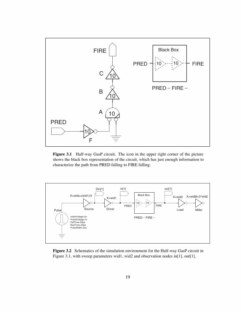
3.2 Step 1: Use Electric to Access the GasP Design
Figure 3.1 shows the schematic diagram of the 6-4 Half-way GasP circuit that we use as
our design example throughout Chapter 3. The circuit name is Half-way GasP because
it represents about half of a 6-4 GasP module in Figure 2.1. The Half-way GasP circuit
has one input pin, PRED, and one output pin, FIRE. Input PRED drives an inverter
called F which subsequently drives a NOR gate called A. The other input to the NOR
gate is grounded. Output FIRE is the output of the NOR gate, delayed by two inversions
through gates B and C. Half-way GasP is a fictional circuit which uses gate size 10 for
all its gates rather than the step-up of 3 sizing strategy of Logical Effort designs [32].
The operation of the Half-way GasP circuit is as follows. When PRED goes low, the
corresponding input to NOR gate A goes high, which results in FIRE going low. The
nominal delay between PRED going low and FIRE going low is about 4 gate delays.
The delay decreases if the output load driven by FIRE decreases or the input drive to
PRED increases. The delay increases if the output load driven by FIRE increases or the
input drive to PRED decreases. Likewise, when PRED goes high, FIRE will go high
after a delay of about 4 gate delays, with a decrease or increase in delay as before. We
will characterize the falling path delay from PRED going low to FIRE going low.
Circuit and path are represented by a black box whose icon is shown in the upper right
corner of Figure 3.1. Only the information that we need from the black box is visible:
• Input PRED and output FIRE, as these connect to the simulation environment.
• Size of initial gate in the path, i.e. 10 (for F), and of final gate, i.e. 10 (for C), as
these determine the sweep sizes for the input driver and output load inverters in
the simulation set-up discussed in the next section.
• The path we’re characterizing: PRED- to FIRE-.
18
PRED
FIRE
10
10
10
10
F
A
B
C
PRED FIRE
Black Box
10 10
PRED FIRE __
Figure 3.1 Half-way GasP circuit. The icon in the upper right corner of the pictureshows the black box representation of the circuit, which has just enough information tocharacterize the path from PRED falling to FIRE falling.
X=wid1
in[1]
Driver SourcePulse
out[1]
X=wid2
PRED FIRE
Load Miller
Din[1]
Black Box
10 10
FallTime=50ps
InitialVoltage=0vPulseVoltage=1v
PulseWidth=2nsRiseTime=50ps
X=wids=(wid1)/3 X=widM=3*wid2
PRED FIRE __
Figure 3.2 Schematics of the simulation environment for the Half-way GasP circuit inFigure 3.1, with sweep parameters wid1, wid2 and observation nodes in[1], out[1].
19

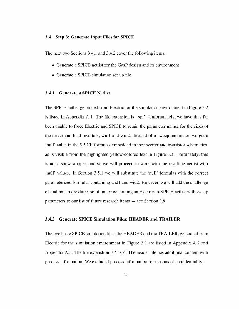
3.3 Step 2: Create a Simulation Environment for the Design
Figure 3.2 shows the schematics of the simulation environment using the black box icon
for the Half-way GasP circuit in Figure 3.1. We use this simulation environment to
generate different input slopes for PRED and different output loads for FIRE. We do
this by generating different driver sizes wid1 for the inverter that drives PRED, and by
using different load sizes wid2 for the inverter that is driven by FIRE. Labels Din[1],
in[1] and out[1] are the observation points for measuring delay and slope information.
We added a pulse generator to start the different simulation measurements — one per
pulse. The generator creates a pulse with a 2ns width and a full-swing slope of 50ps.3.1
Note that we use a series connection of two inverters between the pulse generator and
black box input PRED: a so-called source inverter followed by the already mentioned
driver inverter. Note also the step-down of 3 from the size wid1 of the driver inverter
to the size wids of the source inverter upstream. A step-down of 3 upstream matches
the Logical Effort design strategy [32], and ensures a realistic input slope for the driver
input, independent of the slope generated by the pulse generator. We also use a series
connection of two inverters for the simulation environment at black box output FIRE: a
so-called Miller inverter following the already mentioned load inverter. Note the step-up
of 3 downstream from the size wid2 of the load inverter to the size widM of the Miller
inverter. The step-up of 3 downstream matches the Logical Effort design strategy, and
ensures that the load inverter produces a realistic output load, i.e. it produces just enough
source-to-gate ‘Miller Effect’ for the load inverter as a real environment designed with
Logical Effort would produce for the given load size.3.1A slope of 50ps works fine for this fictitious example. However, for realistic simulation set-ups, we
recommend to use a slope or slew time more typical of a standard inverter operation. For the 90nmCMOSprocess that we currently use, a typical slope for a full signal swing would correspond to 20ps.
20
3.4 Step 3: Generate Input Files for SPICE
The next two Sections 3.4.1 and 3.4.2 cover the following items:
• Generate a SPICE netlist for the GasP design and its environment.
• Generate a SPICE simulation set-up file.
3.4.1 Generate a SPICE Netlist
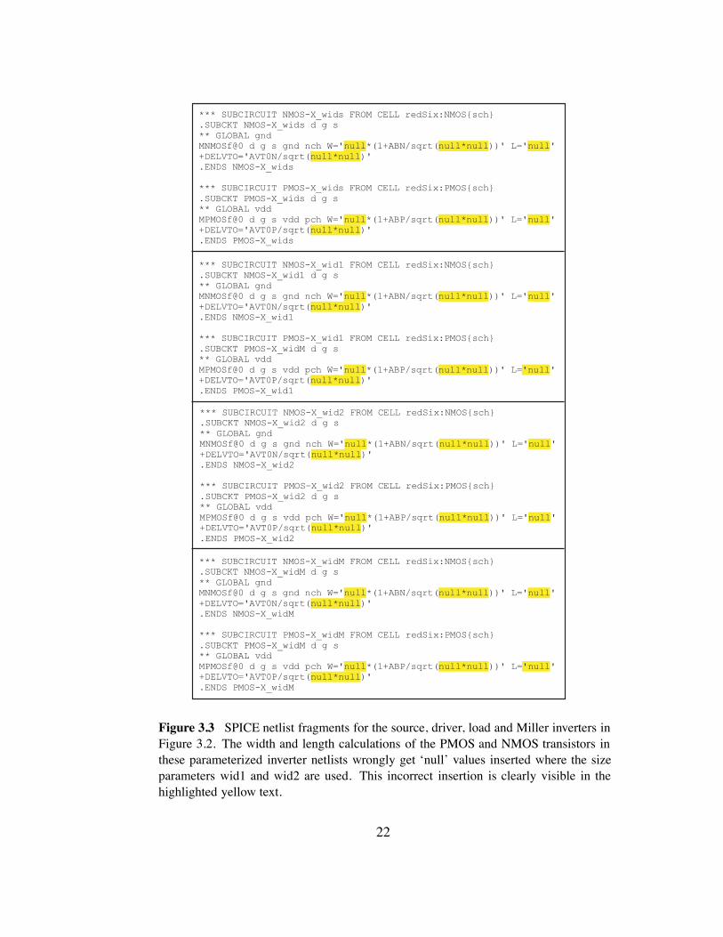
The SPICE netlist generated from Electric for the simulation environment in Figure 3.2
is listed in Appendix A.1. The file extension is ‘.spi’. Unfortunately, we have thus far
been unable to force Electric and SPICE to retain the parameter names for the sizes of
the driver and load inverters, wid1 and wid2. Instead of a sweep parameter, we get a
‘null’ value in the SPICE formulas embedded in the inverter and transistor schematics,
as is visible from the highlighted yellow-colored text in Figure 3.3. Fortunately, this
is not a show-stopper, and so we will proceed to work with the resulting netlist with
‘null’ values. In Section 3.5.1 we will substitute the ‘null’ formulas with the correct
parameterized formulas containing wid1 and wid2. However, we will add the challenge
of finding a more direct solution for generating an Electric-to-SPICE netlist with sweep
parameters to our list of future research items — see Section 3.8.
3.4.2 Generate SPICE Simulation Files: HEADER and TRAILER
The two basic SPICE simulation files, the HEADER and the TRAILER, generated from
Electric for the simulation environment in Figure 3.2 are listed in Appendix A.2 and
Appendix A.3. The file extenstion is ‘.hsp’. The header file has additional content with
process information. We excluded process information for reasons of confidentiality.
21
*** SUBCIRCUIT NMOS-X_wids FROM CELL redSix:NMOS{sch} .SUBCKT NMOS-X_wids d g s ** GLOBAL gnd MNMOSf@0 d g s gnd nch W='null*(1+ABN/sqrt(null*null))' L='null' +DELVTO='AVT0N/sqrt(null*null)' .ENDS NMOS-X_wids *** SUBCIRCUIT PMOS-X_wids FROM CELL redSix:PMOS{sch} .SUBCKT PMOS-X_wids d g s ** GLOBAL vdd MPMOSf@0 d g s vdd pch W='null*(1+ABP/sqrt(null*null))' L='null'+DELVTO='AVT0P/sqrt(null*null)' .ENDS PMOS-X_wids
*** SUBCIRCUIT NMOS-X_wid1 FROM CELL redSix:NMOS{sch} .SUBCKT NMOS-X_wid1 d g s ** GLOBAL gnd MNMOSf@0 d g s gnd nch W='null*(1+ABN/sqrt(null*null))' L='null' +DELVTO='AVT0N/sqrt(null*null)' .ENDS NMOS-X_wid1 *** SUBCIRCUIT PMOS-X_wid1 FROM CELL redSix:PMOS{sch} .SUBCKT PMOS-X_widM d g s ** GLOBAL vdd MPMOSf@0 d g s vdd pch W='null*(1+ABP/sqrt(null*null))' L='null'+DELVTO='AVT0P/sqrt(null*null)' .ENDS PMOS-X_wid1
*** SUBCIRCUIT NMOS-X_wid2 FROM CELL redSix:NMOS{sch} .SUBCKT NMOS-X_wid2 d g s ** GLOBAL gnd MNMOSf@0 d g s gnd nch W='null*(1+ABN/sqrt(null*null))' L='null' +DELVTO='AVT0N/sqrt(null*null)' .ENDS NMOS-X_wid2 *** SUBCIRCUIT PMOS-X_wid2 FROM CELL redSix:PMOS{sch} .SUBCKT PMOS-X_wid2 d g s ** GLOBAL vdd MPMOSf@0 d g s vdd pch W='null*(1+ABP/sqrt(null*null))' L='null' +DELVTO='AVT0P/sqrt(null*null)' .ENDS PMOS-X_wid2
*** SUBCIRCUIT NMOS-X_widM FROM CELL redSix:NMOS{sch} .SUBCKT NMOS-X_widM d g s ** GLOBAL gnd MNMOSf@0 d g s gnd nch W='null*(1+ABN/sqrt(null*null))' L='null' +DELVTO='AVT0N/sqrt(null*null)' .ENDS NMOS-X_widM *** SUBCIRCUIT PMOS-X_widM FROM CELL redSix:PMOS{sch} .SUBCKT PMOS-X_widM d g s ** GLOBAL vdd MPMOSf@0 d g s vdd pch W='null*(1+ABP/sqrt(null*null))' L='null' +DELVTO='AVT0P/sqrt(null*null)' .ENDS PMOS-X_widM
Figure 3.3 SPICE netlist fragments for the source, driver, load and Miller inverters inFigure 3.2. The width and length calculations of the PMOS and NMOS transistors inthese parameterized inverter netlists wrongly get ‘null’ values inserted where the sizeparameters wid1 and wid2 are used. This incorrect insertion is clearly visible in thehighlighted yellow text.
22

3.5 Step 4: Modify the SPICE Input Files
The next two Sections 3.5.1 and 3.5.2 cover the following items:
• In the netlist, create sweep parameters for wid1 and wid2.
• In the simulation set-up files, add sweep and measurement statements.
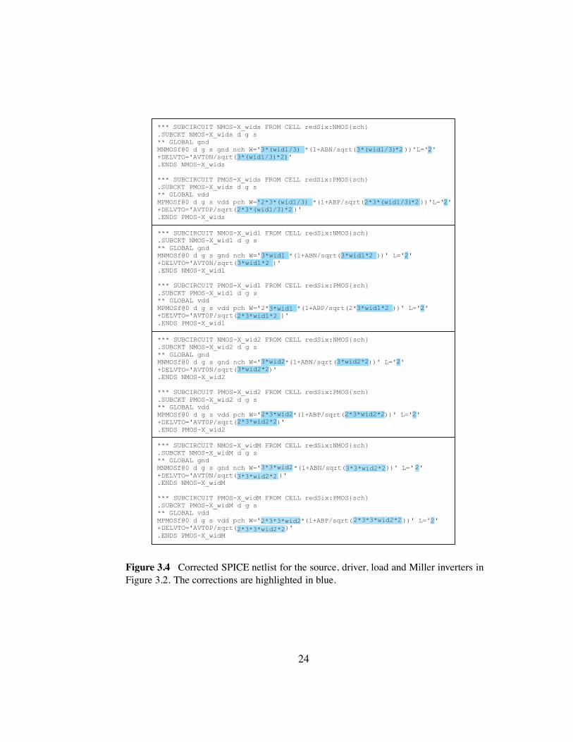
3.5.1 Create Sweep Parameters in the SPICE Netlist
In Section 3.4.1, Figure 3.3, we observed that the parameterized sizes wid1 and wid2
for the driver and load inverters are wrongly expanded into formulas with ‘null’ in the
SPICE netlist parts for the source, driver, load and Miller inverters. We will fix this by
substituting the correct formulas. We can derive the correct formulas from the original
SPICE text in Electric, or simply by looking at the results for the other inverting gates.
Figure 3.4 shows the updated netlist parts with the correct formulas. This substitution
process can be easily automated, using a Perl script.
Note that the formulas have size parameters wid1 and wid2. This will enable us to do
simulation sweeps and generate look up tables for different values of wid1 and wid2.
For completeness and continuity in the Appendices part of this thesis, we have repeated
these corrected SPICE netlist portions in Appendix A.4.
23
*** SUBCIRCUIT NMOS-X_wids FROM CELL redSix:NMOS{sch} .SUBCKT NMOS-X_wids d g s ** GLOBAL gnd MNMOSf@0 d g s gnd nch W='3*(wid1/3) *(1+ABN/sqrt(3*(wid1/3)*2 ))'L='2' +DELVTO='AVT0N/sqrt(3*(wid1/3)*2)' .ENDS NMOS-X_wids *** SUBCIRCUIT PMOS-X_wids FROM CELL redSix:PMOS{sch} .SUBCKT PMOS-X_wids d g s ** GLOBAL vdd MPMOSf@0 d g s vdd pch W='2*3*(wid1/3) *(1+ABP/sqrt(2*3*(wid1/3)*2 ))'L='2'+DELVTO='AVT0P/sqrt(2*3*(wid1/3)*2 )' .ENDS PMOS-X_wids
*** SUBCIRCUIT NMOS-X_wid1 FROM CELL redSix:NMOS{sch} .SUBCKT NMOS-X_wid1 d g s ** GLOBAL gnd MNMOSf@0 d g s gnd nch W='3*wid1 *(1+ABN/sqrt(3*wid1*2 ))' L='2' +DELVTO='AVT0N/sqrt(3*wid1*2 )' .ENDS NMOS-X_wid1 *** SUBCIRCUIT PMOS-X_wid1 FROM CELL redSix:PMOS{sch} .SUBCKT PMOS-X_wid1 d g s ** GLOBAL vdd MPMOSf@0 d g s vdd pch W='2*3*wid1 *(1+ABP/sqrt(2*3*wid1*2 ))' L='2' +DELVTO='AVT0P/sqrt(2*3*wid1*2 )' .ENDS PMOS-X_wid1
*** SUBCIRCUIT NMOS-X_wid2 FROM CELL redSix:NMOS{sch} .SUBCKT NMOS-X_wid2 d g s ** GLOBAL gnd MNMOSf@0 d g s gnd nch W='3*wid2*(1+ABN/sqrt(3*wid2*2))' L='2' +DELVTO='AVT0N/sqrt(3*wid2*2)' .ENDS NMOS-X_wid2 *** SUBCIRCUIT PMOS-X_wid2 FROM CELL redSix:PMOS{sch} .SUBCKT PMOS-X_wid2 d g s ** GLOBAL vdd MPMOSf@0 d g s vdd pch W='2*3*wid2*(1+ABP/sqrt(2*3*wid2*2))' L='2' +DELVTO='AVT0P/sqrt(2*3*wid2*2)' .ENDS PMOS-X_wid2
*** SUBCIRCUIT NMOS-X_widM FROM CELL redSix:NMOS{sch} .SUBCKT NMOS-X_widM d g s ** GLOBAL gnd MNMOSf@0 d g s gnd nch W='3*3*wid2*(1+ABN/sqrt(3*3*wid2*2))' L='2' +DELVTO='AVT0N/sqrt(3*3*wid2*2 )' .ENDS NMOS-X_widM *** SUBCIRCUIT PMOS-X_widM FROM CELL redSix:PMOS{sch} .SUBCKT PMOS-X_widM d g s ** GLOBAL vdd MPMOSf@0 d g s vdd pch W='2*3*3*wid2*(1+ABP/sqrt(2*3*3*wid2*2))' L='2' +DELVTO='AVT0P/sqrt(2*3*3*wid2*2)' .ENDS PMOS-X_widM
Figure 3.4 Corrected SPICE netlist for the source, driver, load and Miller inverters inFigure 3.2. The corrections are highlighted in blue.
24
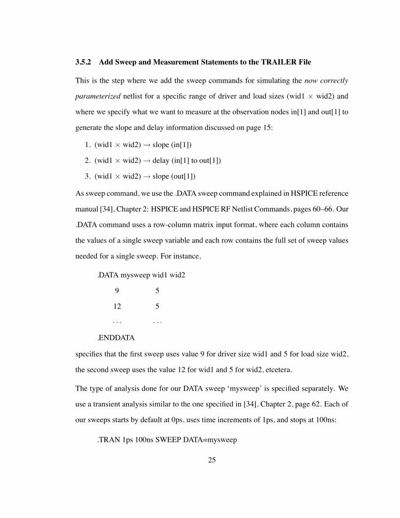
3.5.2 Add Sweep and Measurement Statements to the TRAILER File
This is the step where we add the sweep commands for simulating the now correctly
parameterized netlist for a specific range of driver and load sizes (wid1 # wid2) and
where we specify what we want to measure at the observation nodes in[1] and out[1] to
generate the slope and delay information discussed on page 15:
1. (wid1 # wid2)$ slope (in[1])
2. (wid1 # wid2)$ delay (in[1] to out[1])
3. (wid1 # wid2)$ slope (out[1])
As sweep command, we use the .DATA sweep command explained in HSPICE reference
manual [34], Chapter 2: HSPICE and HSPICE RF Netlist Commands, pages 60–66. Our
.DATA command uses a row-column matrix input format, where each column contains
the values of a single sweep variable and each row contains the full set of sweep values
needed for a single sweep. For instance,
.DATA mysweep wid1 wid2
9 5
12 5
· · · · · ·
.ENDDATA
specifies that the first sweep uses value 9 for driver size wid1 and 5 for load size wid2,
the second sweep uses the value 12 for wid1 and 5 for wid2, etcetera.
The type of analysis done for our DATA sweep ‘mysweep’ is specified separately. We
use a transient analysis similar to the one specified in [34], Chapter 2, page 62. Each of
our sweeps starts by default at 0ps, uses time increments of 1ps, and stops at 100ns:
.TRAN 1ps 100ns SWEEP DATA=mysweep
25
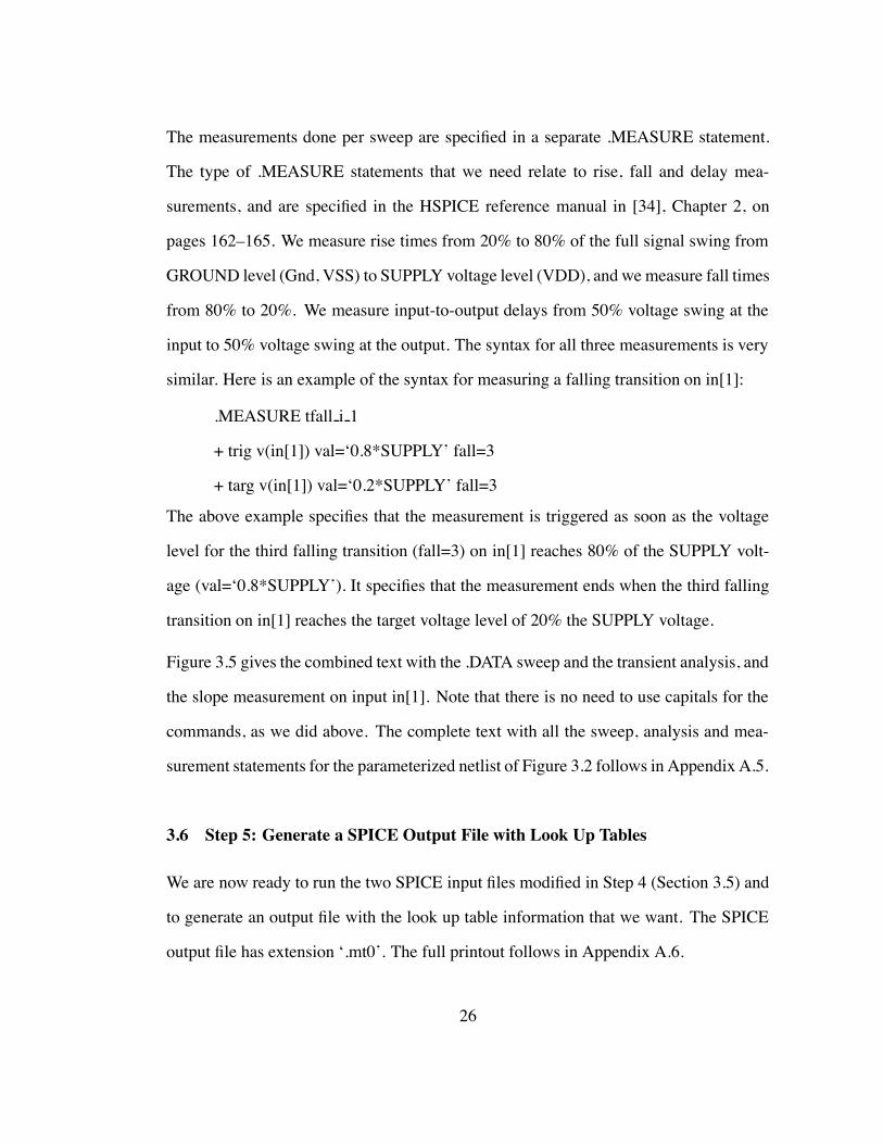
The measurements done per sweep are specified in a separate .MEASURE statement.
The type of .MEASURE statements that we need relate to rise, fall and delay mea-
surements, and are specified in the HSPICE reference manual in [34], Chapter 2, on
pages 162–165. We measure rise times from 20% to 80% of the full signal swing from
GROUND level (Gnd, VSS) to SUPPLY voltage level (VDD), and we measure fall times
from 80% to 20%. We measure input-to-output delays from 50% voltage swing at the
input to 50% voltage swing at the output. The syntax for all three measurements is very
similar. Here is an example of the syntax for measuring a falling transition on in[1]:
.MEASURE tfall i 1
+ trig v(in[1]) val=‘0.8*SUPPLY’ fall=3
+ targ v(in[1]) val=‘0.2*SUPPLY’ fall=3
The above example specifies that the measurement is triggered as soon as the voltage
level for the third falling transition (fall=3) on in[1] reaches 80% of the SUPPLY volt-
age (val=‘0.8*SUPPLY’). It specifies that the measurement ends when the third falling
transition on in[1] reaches the target voltage level of 20% the SUPPLY voltage.
Figure 3.5 gives the combined text with the .DATA sweep and the transient analysis, and
the slope measurement on input in[1]. Note that there is no need to use capitals for the
commands, as we did above. The complete text with all the sweep, analysis and mea-
surement statements for the parameterized netlist of Figure 3.2 follows in Appendix A.5.
3.6 Step 5: Generate a SPICE Output File with Look Up Tables
We are now ready to run the two SPICE input files modified in Step 4 (Section 3.5) and
to generate an output file with the look up table information that we want. The SPICE
output file has extension ‘.mt0’. The full printout follows in Appendix A.6.
26
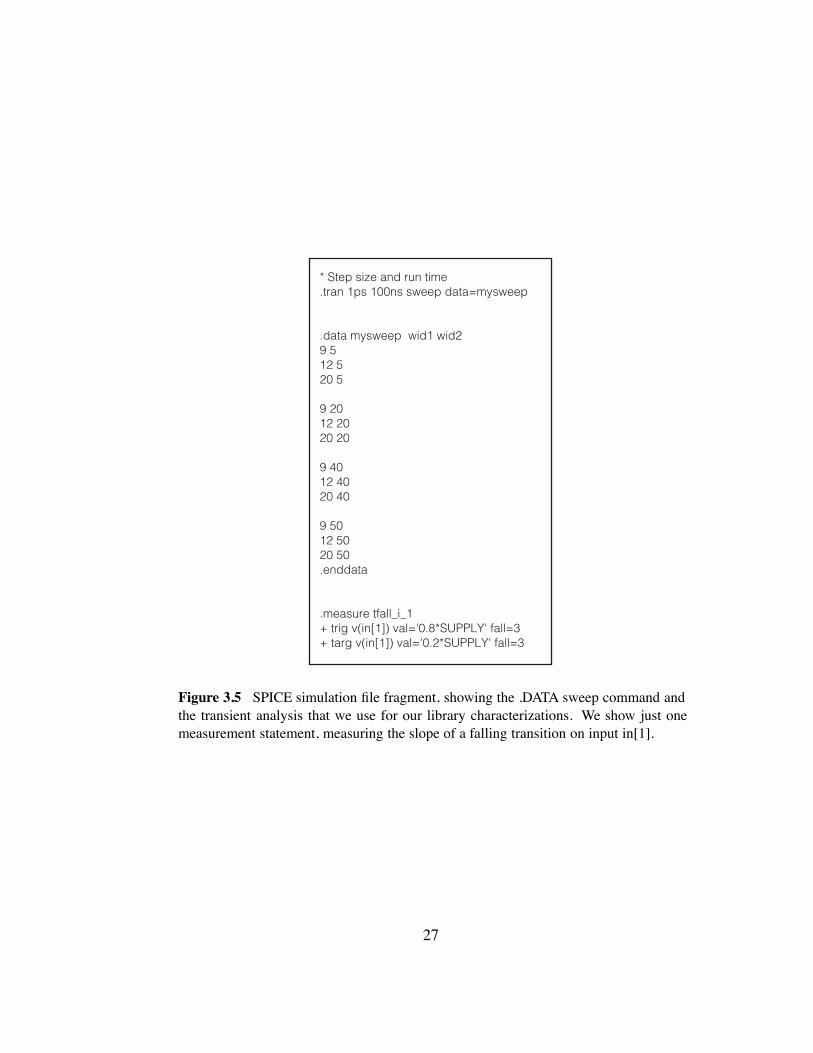
* Step size and run time .tran 1ps 100ns sweep data=mysweep
.data mysweep wid1 wid29 512 520 5
9 2012 2020 20
9 4012 4020 40
9 5012 5020 50.enddata
.measure tfall_i_1+ trig v(in[1]) val='0.8*SUPPLY' fall=3+ targ v(in[1]) val='0.2*SUPPLY' fall=3
Figure 3.5 SPICE simulation file fragment, showing the .DATA sweep command andthe transient analysis that we use for our library characterizations. We show just onemeasurement statement, measuring the slope of a falling transition on input in[1].
27
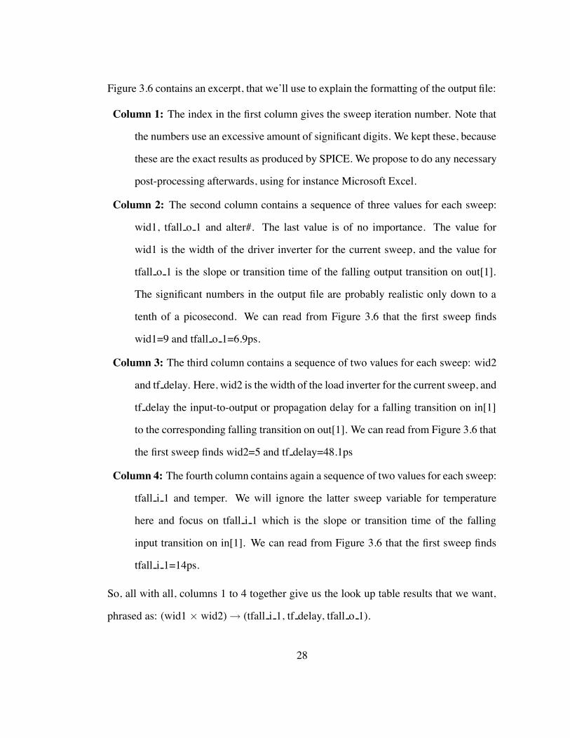
Figure 3.6 contains an excerpt, that we’ll use to explain the formatting of the output file:
Column 1: The index in the first column gives the sweep iteration number. Note that
the numbers use an excessive amount of significant digits. We kept these, because
these are the exact results as produced by SPICE. We propose to do any necessary
post-processing afterwards, using for instance Microsoft Excel.
Column 2: The second column contains a sequence of three values for each sweep:
wid1, tfall o 1 and alter#. The last value is of no importance. The value for
wid1 is the width of the driver inverter for the current sweep, and the value for
tfall o 1 is the slope or transition time of the falling output transition on out[1].
The significant numbers in the output file are probably realistic only down to a
tenth of a picosecond. We can read from Figure 3.6 that the first sweep finds
wid1=9 and tfall o 1=6.9ps.
Column 3: The third column contains a sequence of two values for each sweep: wid2
and tf delay. Here, wid2 is the width of the load inverter for the current sweep, and
tf delay the input-to-output or propagation delay for a falling transition on in[1]
to the corresponding falling transition on out[1]. We can read from Figure 3.6 that
the first sweep finds wid2=5 and tf delay=48.1ps
Column 4: The fourth column contains again a sequence of two values for each sweep:
tfall i 1 and temper. We will ignore the latter sweep variable for temperature
here and focus on tfall i 1 which is the slope or transition time of the falling
input transition on in[1]. We can read from Figure 3.6 that the first sweep finds
tfall i 1=14ps.
So, all with all, columns 1 to 4 together give us the look up table results that we want,
phrased as: (wid1 # wid2)$ (tfall i 1, tf delay, tfall o 1).
28
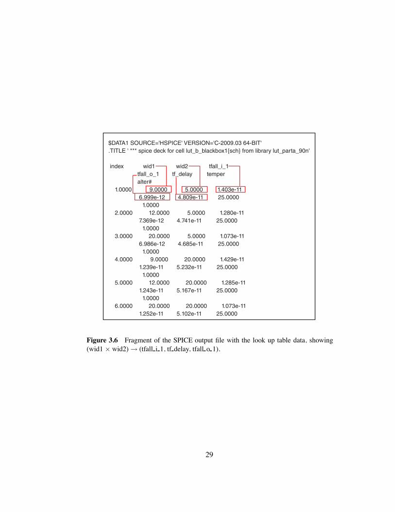
$DATA1 SOURCE='HSPICE' VERSION='C-2009.03 64-BIT'.TITLE ' *** spice deck for cell lut_b_blackbox1{sch} from library lut_parta_90n'
index wid1 wid2 tfall_i_1 tfall_o_1 tf_delay temper alter# 1.0000 9.0000 5.0000 1.403e-11 6.999e-12 4.809e-11 25.0000 1.0000 2.0000 12.0000 5.0000 1.280e-11 7.369e-12 4.741e-11 25.0000 1.0000 3.0000 20.0000 5.0000 1.073e-11 6.986e-12 4.685e-11 25.0000 1.0000 4.0000 9.0000 20.0000 1.429e-11 1.239e-11 5.232e-11 25.0000 1.0000 5.0000 12.0000 20.0000 1.285e-11 1.243e-11 5.167e-11 25.0000 1.0000 6.0000 20.0000 20.0000 1.073e-11 1.252e-11 5.102e-11 25.0000
Figure 3.6 Fragment of the SPICE output file with the look up table data, showing(wid1 # wid2)$ (tfall i 1, tf delay, tfall o 1).
29
3.7 Validation
In the introduction Section 3.1, we indicated that there are two ways to sweep the search
key values for (wid1 # wid2) and to generate the resulting delay and slope information
for a simple path in a GasP circuit. ‘Way one’ is to do the sweep work at design time
in Electric, and ‘way two’ is to do the sweep work in SPICE. We followed ‘way two’
because the alternative produces much larger SPICE output file sizes. In this section,
we compare our results against the results obtained with ‘way one’.
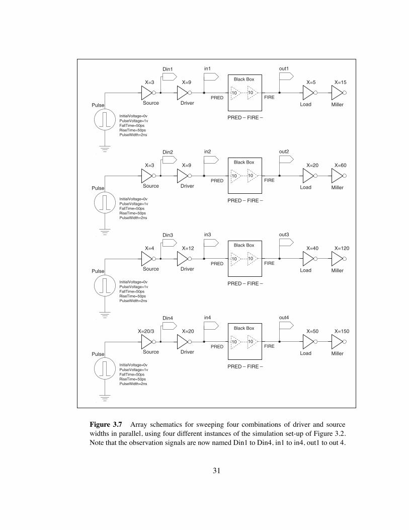
Figure 3.7 shows four out of the total of twelve sweeps that we ran, covering all possible
driver sizes and all possible load sizes, but only four combinations of driver and load
sizes. The four sweeps appear as four parallel designs, all designed in Electric. SPICE
will run all four designs in parallel. It does this without needing a .DATA sweep com-
mand. However, we do need to specify analysis and measurement statements. So, the
original five steps that were needed for ‘way two’ can be simplified to:
Step 1: (as before) Use Electric to access the GasP design of Figure 3.1.
Step 2: In Electric, create Figure 3.7 with parallel design sweep environments.
Step 3: (as before) From Electric, generate input files for SPICE:
• Generate a SPICE netlist for the GasP design and its environment.
• Generate a SPICE simulation set-up file.
Step 4: Modify only the SPICE simulation set-up file:
• Add transient analysis and measurement statements.
Step 5: Run SPICE and capture the look up table results in an output file.
The corresponding SPICE input and output files follow in Appendix B.
30
X=9
in1
Driver SourcePulse
out1
X=5
PRED FIRE
Load Miller
Din1
Black Box
10 10
FallTime=50ps
InitialVoltage=0vPulseVoltage=1v
PulseWidth=2nsRiseTime=50ps
X=3 X=15
PRED FIRE __
X=9
in2
Driver SourcePulse
out2
X=20
PRED FIRE
Load Miller
Din2
Black Box
10 10
FallTime=50ps
InitialVoltage=0vPulseVoltage=1v
PulseWidth=2nsRiseTime=50ps
X=3 X=60
PRED FIRE __
X=12
in3
Driver SourcePulse
out3
X=40
PRED FIRE
Load Miller
Din3
Black Box
10 10
FallTime=50ps
InitialVoltage=0vPulseVoltage=1v
PulseWidth=2nsRiseTime=50ps
X=4 X=120
PRED FIRE __
X=20
in4
Driver SourcePulse
out4
X=50
PRED FIRE
Load Miller
Din4
Black Box
10 10
FallTime=50ps
InitialVoltage=0vPulseVoltage=1v
PulseWidth=2nsRiseTime=50ps
X=20/3 X=150
PRED FIRE __
Figure 3.7 Array schematics for sweeping four combinations of driver and sourcewidths in parallel, using four different instances of the simulation set-up of Figure 3.2.Note that the observation signals are now named Din1 to Din4, in1 to in4, out1 to out 4.
31
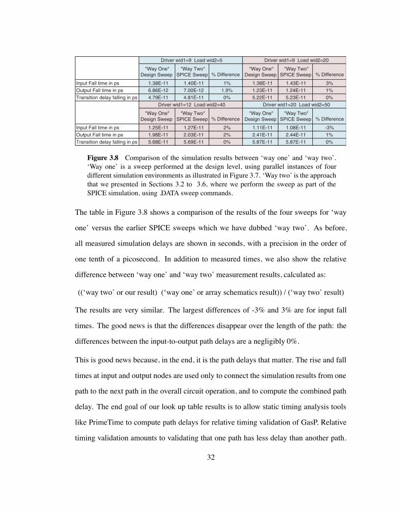
Driver wid1=9 Load wid2=5 Driver wid1=9 Load wid2=20
% Difference % Difference
Input Fall time in ps 1.38E-11 1.40E-11 1% 1.38E-11 1.43E-11 3%Output Fall time in ps 6.86E-12 7.00E-12 1.9% 1.23E-11 1.24E-11 1%Transition delay falling in ps 4.79E-11 4.81E-11 0% 5.22E-11 5.23E-11 0%
Driver wid1=12 Load wid2=40 Driver wid1=20 Load wid2=50
% Difference % Difference
Input Fall time in ps 1.25E-11 1.27E-11 2% 1.11E-11 1.08E-11 -3%Output Fall time in ps 1.98E-11 2.03E-11 2% 2.41E-11 2.44E-11 1%Transition delay falling in ps 5.68E-11 5.69E-11 0% 5.87E-11 5.87E-11 0%
"Way One"Design Sweep
"Way One"Design Sweep
"Way Two"SPICE Sweep
"Way Two"SPICE Sweep
"Way One"Design Sweep
"Way One"Design Sweep
"Way Two"SPICE Sweep
"Way Two"SPICE Sweep
Figure 3.8 Comparison of the simulation results between ‘way one’ and ‘way two’.‘Way one’ is a sweep performed at the design level, using parallel instances of fourdifferent simulation environments as illustrated in Figure 3.7. ‘Way two’ is the approachthat we presented in Sections 3.2 to 3.6, where we perform the sweep as part of theSPICE simulation, using .DATA sweep commands.
The table in Figure 3.8 shows a comparison of the results of the four sweeps for ‘way
one’ versus the earlier SPICE sweeps which we have dubbed ‘way two’. As before,
all measured simulation delays are shown in seconds, with a precision in the order of
one tenth of a picosecond. In addition to measured times, we also show the relative
difference between ‘way one’ and ‘way two’ measurement results, calculated as:
((‘way two’ or our result) (‘way one’ or array schematics result)) / (‘way two’ result)
The results are very similar. The largest differences of -3% and 3% are for input fall
times. The good news is that the differences disappear over the length of the path: the
differences between the input-to-output path delays are a negligibly 0%.
This is good news because, in the end, it is the path delays that matter. The rise and fall
times at input and output nodes are used only to connect the simulation results from one
path to the next path in the overall circuit operation, and to compute the combined path
delay. The end goal of our look up table results is to allow static timing analysis tools
like PrimeTime to compute path delays for relative timing validation of GasP. Relative
timing validation amounts to validating that one path has less delay than another path.
32
Given this background knowledge and the results in Figure 3.8, we may conclude that
a difference of 3% for the input slope of a path is not going to matter. In summary: the
results obtained via ‘way one’ are similar to those obtained by ‘way two’.
3.8 Conclusion and Future Work for Chapter 3
We created a characterization flow for generating look up tables with timing information
for a simple input-to-output transition in a simplified 6-4 GasP circuit. This chapter is
dubbed ‘PART-A’ because it has a follow-up part. PART-B, in the next chapter, shows
how to characterize a complete 6-4 GasP module. In PART-B, we will partition the
behavior of a 6-4 GasP FIFO circuit into simple input-to-output transitions and simpli-
fied circuits that can be fed back into the library characterization flow developed here in
PART-A. Given that “the proof of the pudding is in the eating”, we will feed the look up
tables that we generate in PART-B to a standard static timing analysis tool to validate
the relative timing constrains of the 6-4 GasP FIFO module. This happens in Chapter 5.
As far as future work goes, the characterization flow in PART-A can benefit from:
1. Flow automation:
• We need templates for Steps 1–2, to automate the creation of simulation
environments like Figure 3.2 and 3.7, for different GasP circuits in Electric.
• We need scripts to automate the SPICE simulation part in Steps 3–5.
2. A direct solution for creating sweep variables wid1 and wid2 for the driver and
load inverters in the simulation environment at the schematic level of Electric:
• Currently, Electric produces ‘null’ values for the sweep parameters wid1 and
wid2 in Figure 3.2. This is visible from the SPICE netlist that we generate
in Step 3. We correct this in Step 4, but it would be much better to avoid the
need for such a correction.
33
Chapter 4
LIBRARY CHARACTERIZATION PART-B: FROM GASP TO LUTs
Chapter 4 is also available as internal report ARC2010-smg02 [17]. It is the second
of a two-part solution to create look up tables that accurately characterize the timing
information of a 6-4 GasP circuit. PART-A in the previous Chapter 3 takes a simple
circuit without timing loops, and shows the basic flow aspects from the schematics entry
level of the design in Electric to the SPICE simulation set-up and the SPICE output
files with the look up tables. PART-B, described here, shows how to partition complex
circuits with timing loops and multiple inputs and outputs into designs for which the
timing is simple enough to be handled by the characterization flow in PART-A.
4.1 Introduction
In PART-A, presented in Chapter 3 and available as report ARC2010-smg01 [16], we
showed how one can use SPICE to generate look up tables with timing information of
a 6-4 GasP circuit. We generated look up tables for input-to-output propagation times
and slew times, a.k.a. slopes or rise and fall times, under various input slopes and output
loads. We used a 6-4 GasP sub-circuit, called Half-way GasP, to illustrate the approach.
PART-A focused on simple input-to-output paths. PART-B, presented here, extends
PART-A, by explaining how to deal with complex paths. We illustrate this extension on
the full-fledged 6-4 GasP FIFO design of Figure 2.1 on page 11.
34
For complex paths with loops or multiple input and output ports we use a two-step
procedure. In the first step, called STEP 1 below, we break the path into a sequence
of input-to-output paths, each simple enough to fit in the solution approach of PART-A.
In the second step, called STEP 2 below, we show how one should simulate the simple
paths to guarantee that the sum of the look up table entries for the propagation times
through the simple paths is a sufficiently accurate approximation of the propagation
time through the complex path. STEP 2 introduces a unique problem that stems from
the single-track handshake protocol in 6-4 GasP: any simple path ending at a single-track
output signal is left un-driven at the end of an input pulse. This prevents us from running
multiple simulation cycles per sweep — and we typically run a few cycles before we
start measuring to get beyond initialization issues. We solve this problem by adding a
VCCS device to re-initialize the ouput signal without extra load or delay to the signal.
The solution follows in Section 4.4.2.2.
We deploy the look up tables generated with this combined PART-A and PART-B ap-
proach to analyze and validate so-called ‘Relative Timing’ constraints in GasP using
standard static timing analysis (STA) tools. Relative timing constraints describe the or-
der in which two signals must arrive at a point of convergence [27, 28]. Specifically:
relative timing constraints require that the maximum path delay for the fast signal is
below the minimum path delay for the slow signal. This implies that our look up tables
must characterize maximum and minimum path delays. This implication simplifies the
characterization process because we can ignore all of the intermediary delay scenarios.
We use this fact in the naming convention of paths, to express whether the path describes
a fast or slow signal. We also use it to incorporate ‘The Charlie Effect’ [1] into our sim-
ulation setup. We use ‘The Charlie Effect’only to obtain a maximum or minimum delay
35
setup, where needed. For the timing constraints that we characterize and analyze in this
thesis, it sufficed to simulate a minimal falling gate delay for gate A in Figure 2.1. We
do this by adding a VCVS device. The device enables us to synchronize input events for
gates with multiple input signals, without adding extra load or delay. The synchronized
(rising) inputs to gate A create a minimal (falling) gate delay for A, which is exactly
what we need for the relative timing constraints evaluated in this thesis. The solution
follows in Section 4.4.2.1.
The organization of the remainder of Chapter 4 is as follows. Section 4.2 is a quick
reminder of what a look up table is and how it is used. Section 4.3 explains STEP 1 of
our two-step procedure: how to partition complex circuit paths with loops and multiple
input and output ports into simple paths without loops and with one input and one out-
put. Section 4.4 explains STEP 2 of our two-step procedure: how to simulate simple
input-to-output paths with sufficient accuracy so that the generated look up tables are a
good black box representation for maximum and minimum input-to-output propagation
delays and input and output slopes. Section 4.5 generalizes the simulation setup and
solves outstanding issues that we encountered in PART-B while using the simulation
setup presented in PART-A. Section 4.6 concludes this Chapter 4. Appendices C to H
contain the SPICE simulation files generated in STEP 2.
Note:
We postpone the comparison between our library characterization work and prior work
at USC by Mallika Prakash [21, 22] and Prasad Joshi [2, 3] to Chapter 7.
36
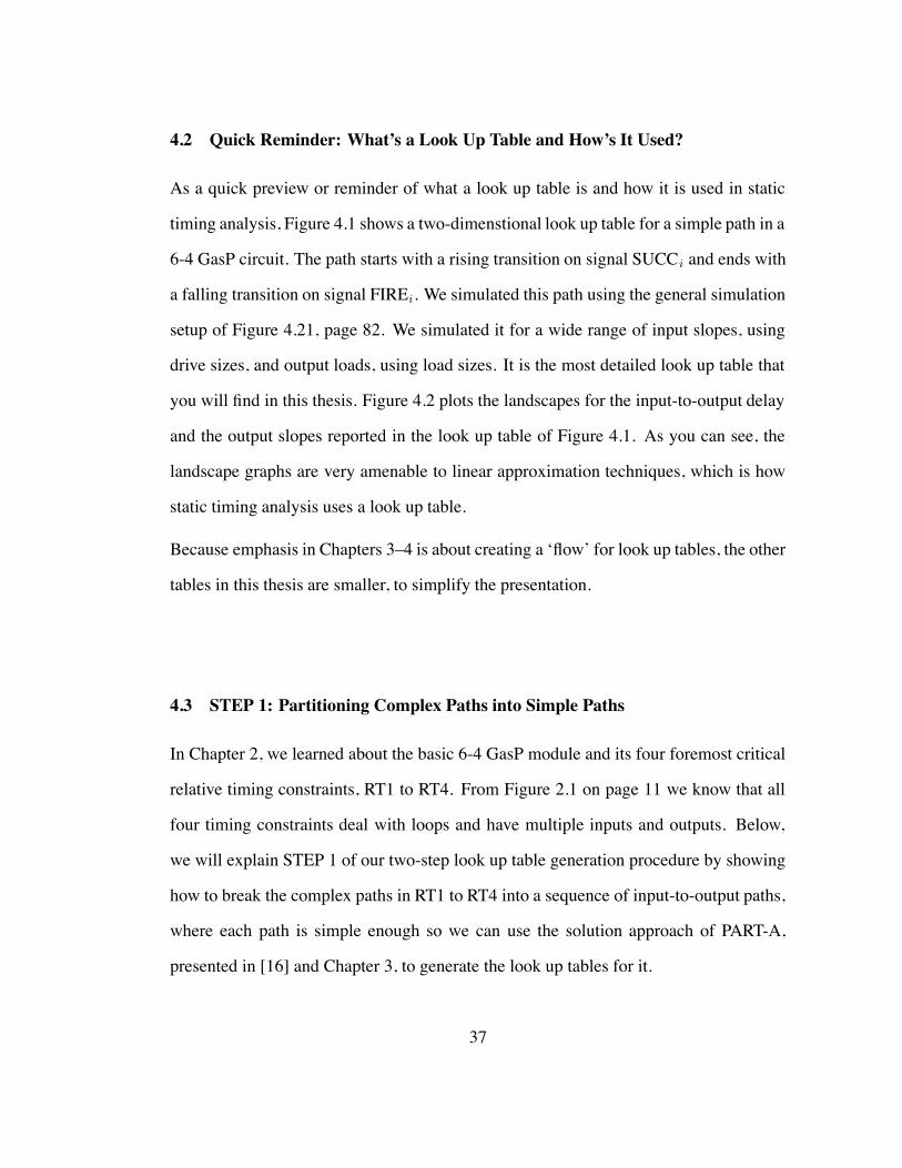
4.2 Quick Reminder: What’s a Look Up Table and How’s It Used?
As a quick preview or reminder of what a look up table is and how it is used in static
timing analysis, Figure 4.1 shows a two-dimenstional look up table for a simple path in a
6-4 GasP circuit. The path starts with a rising transition on signal SUCCi and ends with
a falling transition on signal FIREi. We simulated this path using the general simulation
setup of Figure 4.21, page 82. We simulated it for a wide range of input slopes, using
drive sizes, and output loads, using load sizes. It is the most detailed look up table that
you will find in this thesis. Figure 4.2 plots the landscapes for the input-to-output delay
and the output slopes reported in the look up table of Figure 4.1. As you can see, the
landscape graphs are very amenable to linear approximation techniques, which is how
static timing analysis uses a look up table.
Because emphasis in Chapters 3–4 is about creating a ‘flow’ for look up tables, the other
tables in this thesis are smaller, to simplify the presentation.
4.3 STEP 1: Partitioning Complex Paths into Simple Paths
In Chapter 2, we learned about the basic 6-4 GasP module and its four foremost critical
relative timing constraints, RT1 to RT4. From Figure 2.1 on page 11 we know that all
four timing constraints deal with loops and have multiple inputs and outputs. Below,
we will explain STEP 1 of our two-step look up table generation procedure by showing
how to break the complex paths in RT1 to RT4 into a sequence of input-to-output paths,
where each path is simple enough so we can use the solution approach of PART-A,
presented in [16] and Chapter 3, to generate the look up tables for it.
37
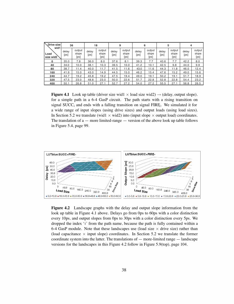
36 18 9 6 5 4
0 35.0 7.8 36.0 8.0 37.6 8.1 39.3 7.7 40.6 7.7 42.2 8.040 34.0 10.0 38.1 10.3 39.5 10.0 41.2 10.1 42.5 9.8 44.0 9.980 38.7 11.4 40.0 11.7 41.5 11.6 43.0 11.6 44.3 11.8 46.0 12.4
160 41.9 15.0 43.0 14.9 44.5 15.0 46.2 15.4 47.6 15.2 49.0 15.6240 44.7 19.2 45.8 19.2 47.5 19.4 49.0 19.1 50.2 19.1 51.7 18.9320 47.5 23.0 48.8 23.0 50.0 22.6 51.7 22.8 52.8 22.8 54.4 23.2400 50.1 26.8 51.0 27.1 52.7 27.2 54.0 27.2 55.5 27.1 56.8 26.5
delay[ps]
outputslope[ps]
delay[ps]
outputslope[ps]
delay[ps]
outputslope[ps]
delay[ps]
outputslope[ps]
delay[ps]
outputslope[ps]
delay[ps]
outputslope[ps]
Loadsize wid2
Drive size wid1
Figure 4.1 Look up table (driver size wid1 # load size wid2)$ (delay, output slope).for a simple path in a 6-4 GasP circuit. The path starts with a rising transition onsignal SUCCi and ends with a falling transition on signal FIREi. We simulated it fora wide range of input slopes (using drive sizes) and output loads (using load sizes).In Section 5.2 we translate (wid1 # wid2) into (input slope # output load) coordinates.The translation of a —more limited-range — version of the above look up table followsin Figure 5.4, page 99.
Figure 4.2 Landscape graphs with the delay and output slope information from thelook up table in Figure 4.1 above. Delays go from 0ps to 60ps with a color distinctionevery 10ps, and output slopes from 0ps to 30ps with a color distinction every 5ps. Wedropped the index ‘i’ from the path name, because the path is fully contained within a6-4 GasP module. Note that these landscapes use (load size # drive size) rather than(load capacitance # input slope) coordinates. In Section 5.2 we translate the formercoordinate system into the latter. The translations of—more-limited range— landscapeversions for the landscapes in this Figure 4.2 follow in Figure 5.9(top), page 104.
38
The caveat is that look up tables deal with circuit parameters that can be measured
reasonably well in advance. For instance, it takes reasonably low effort to make ac-
curate look up tables that capture the internal path delays in modules M1 and M2 of
Figure 2.1. Capturing these internal path delays takes hardly any effort, because each
module is a hard macro with pre-defined internal loads, internal wire lengths, and inter-
nal drive strengths — custom-designed according to the theory of Logical Effort [32].
But to make an accurate look up table that captures the path delay through state wire L2
between modules M1 and M2 is a tremendous amount of work, because (1) we do not
know the exact length and width and spacing of L2 until the system has been placed and
routed, and (2) the dependency of the state wire delay to layout wire parameters such as
length, width and spacing becomes more complex with longer wires, as we show in [18].
To ensure that timing analysis and relative timing validation for GasP are both accurate
and practical, we are going to leave the delay and slope measurements associated with
state wire L2 to static timing analysis (STA) with back-annotated wire information from
the final layout results. In the partitioning method, to be presented below, we will in-
dicate which of the final paths we are going to leave to STA, and which ones we will
characterize using the LUT or look up table approach.
To partition the paths, we first cut them at basic input-output signals, because these
are the points where external drives and loads are attached. For our example circuit in
Figure 2.1 with its four relative timing constraints in Figure 2.2, the basic input-output
signals are PRED1, SUCC1, FIRE1 and PRED2, SUCC2, FIRE2. We will introduce
a few more input-output signals, to control or observe the delay and slope simulation
measurements as we go along. The partitioning for the paths that constitute each relative
timing constraint follows in Figures 4.3–4.6.
39
We will explain our partitioning strategy using the partitioning for RT1 in Figure 4.3.
Figure 4.3 partitions the complex paths in RT1 into simple input-to-output paths. The
graph at the top is a copy of the graphical representation for RT1 from Figure 2.2(a).
It shows a red-arrow path, which we will simply call the red path, and it shows a blue-
arrow path, which we will simply call the blue path. RT1 requires that the red path delay
is less than the blue path delay.
We cut the red path of RT1 at the basic input-output signals FIRE1, SUCC1 and PRED2.
This yields two simple paths, indicated by the two graphs below the fat black arrow on
the right and separated by a fat ‘+’ sign, shown in Figure 4.3 . For the first path we can
reasonably well measure input-to-output delays and slopes and capture these in look up
tables. We named this path LUTred:FIRE1+SUCC1+. Note that the name keeps the
information about the path color, namely red, and about how the timing is captured,
namely by LUT or look up table. The color is important for the simulation set-up: the
(maximum) total delay of the red path must be less than the (minimum) total delay of
the blue path, and so for red paths we are interested in simulating maximum delays. The
second path goes through state wire L2, and so, we are going to leave its delay and slope
measurements to STA or static timing analysis with back-annotated wire information
from the final layout results. We named this second path STAred:SUCC1+PRED2+.
Note that also this name keeps the information about the path color, namely red, and
about how the information is to be captured, namely by STA.
We initially cut the blue path of RT1 at the basic input-output signals FIRE1, PRED1 and
SUCC1. This yields three paths, indicated by the three graphs below the fat black arrow
on the left and separated by a fat ‘+’ sign. For the first two paths we can reasonably well
measure input-to-output delays and slopes and capture these in look up tables.
40
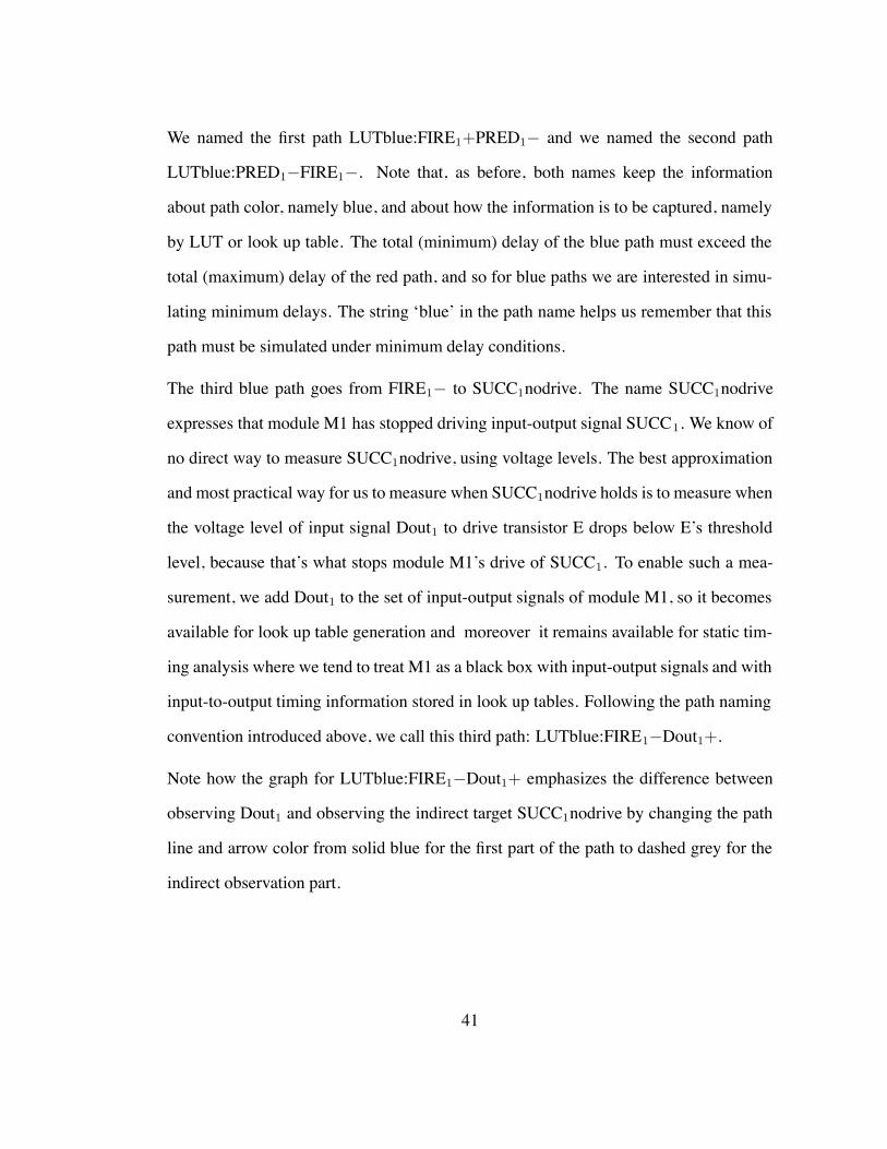
We named the first path LUTblue:FIRE1+PRED1" and we named the second path
LUTblue:PRED1"FIRE1". Note that, as before, both names keep the information
about path color, namely blue, and about how the information is to be captured, namely
by LUT or look up table. The total (minimum) delay of the blue path must exceed the
total (maximum) delay of the red path, and so for blue paths we are interested in simu-
lating minimum delays. The string ‘blue’ in the path name helps us remember that this
path must be simulated under minimum delay conditions.
The third blue path goes from FIRE1" to SUCC1nodrive. The name SUCC1nodrive
expresses that module M1 has stopped driving input-output signal SUCC1. We know of
no direct way to measure SUCC1nodrive, using voltage levels. The best approximation
and most practical way for us to measure when SUCC1nodrive holds is to measure when
the voltage level of input signal Dout1 to drive transistor E drops below E’s threshold
level, because that’s what stops module M1’s drive of SUCC1. To enable such a mea-
surement, we add Dout1 to the set of input-output signals of module M1, so it becomes
available for look up table generation and moreover it remains available for static tim-
ing analysis where we tend to treat M1 as a black box with input-output signals and with
input-to-output timing information stored in look up tables. Following the path naming
convention introduced above, we call this third path: LUTblue:FIRE1"Dout1+.
Note how the graph for LUTblue:FIRE1"Dout1+ emphasizes the difference between
observing Dout1 and observing the indirect target SUCC1nodrive by changing the path
line and arrow color from solid blue for the first part of the path to dashed grey for the
indirect observation part.
41

FIRE1+FIRE1-
PRED1- SUCC1+
A
B
C
X
F
E
D
E
D
SUCC1nodrivePRED2+
M1 M2
RT(L2)TrfF-RstB : red path < blue path
L2
FIRE1+
PRED1-
PRED1-
X
FIRE1-
A
B
C
F
FIRE1-
FIRE1+
SUCC1+
E
D
SUCC1+ PRED2+L2
D
LUTblue : FIRE1+ PRED1-
LUTblue : PRED1- FIRE1-
LUTblue : FIRE1- Dout1+
LUTred : FIRE1+ SUCC1+
STAred : SUCC1+ PRED2+
Dout1+
SUCCSUCC1nodrivenodrive
E
M1
M1
M1
M1
M1 M2
+
+
+
Figure 4.3 Partitioning of the complex paths in relative timing constraint RT1 orRT(L2)TrfF!RstB of Figure 2.2(a) into simple timing paths for its blue path (left) andfor its red path (right).
42
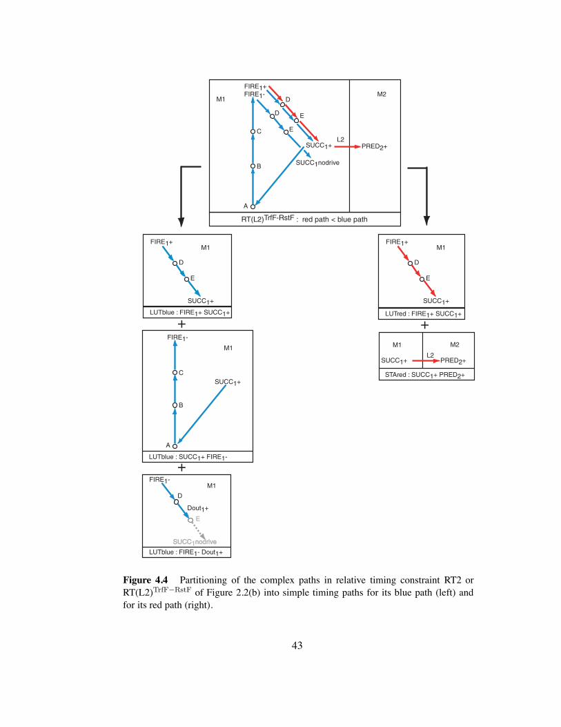
FIRE1-
A
B
C
FIRE1-
FIRE1+
SUCC1+
E
D
SUCC1+ PRED2+L2
D
LUTblue : SUCC1+ FIRE1-
LUTblue : FIRE1- Dout1+
LUTred : FIRE1+ SUCC1+
STAred : SUCC1+ PRED2+
Dout1+
SUCCSUCC1nodrivenodrive
E
M1
M1FIRE1+
SUCC1+
E
D
LUTblue : FIRE1+ SUCC1+
M1
M1 M2
+
+
+
E
D
FIRE1+FIRE1-
SUCC1+
A
B
C
PRED2+
SUCC1nodrive
E
DM1M2
RT(L2)TrfF-RstF : red path < blue path
L2
SUCC1+
M1
Figure 4.4 Partitioning of the complex paths in relative timing constraint RT2 orRT(L2)TrfF!RstF of Figure 2.2(b) into simple timing paths for its blue path (left) andfor its red path (right).
43
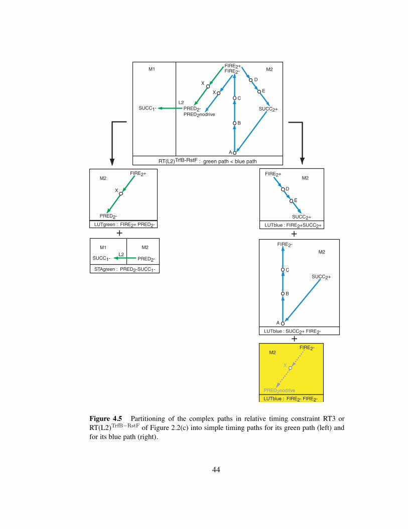
L2
STAgreen : PRED2-SUCC1-
M1 M2
+
FIRE2-
LUTblue : FIRE2- FIRE2-
M2
FIRE2+
PRED2-
X
LUTgreen : FIRE2+ PRED2-
M2
+
PRED2-SUCC1-
PREDPRED2nodrivenodrive
X
A
B
C
FIRE2+FIRE2-
PRED2-PRED2nodrive
SUCC2+
X
E
D
SUCC1-
X
RT(L2)TrfB-RstF : green path < blue path
L2
M1 M2
FIRE2-
A
B
C
LUTblue : SUCC2+ FIRE2-
FIRE2+
SUCC2+
E
D
LUTblue : FIRE2+SUCC2+
M2
+
SUCC2+
M2
Figure 4.5 Partitioning of the complex paths in relative timing constraint RT3 orRT(L2)TrfB!RstF of Figure 2.2(c) into simple timing paths for its green path (left) andfor its blue path (right).
44
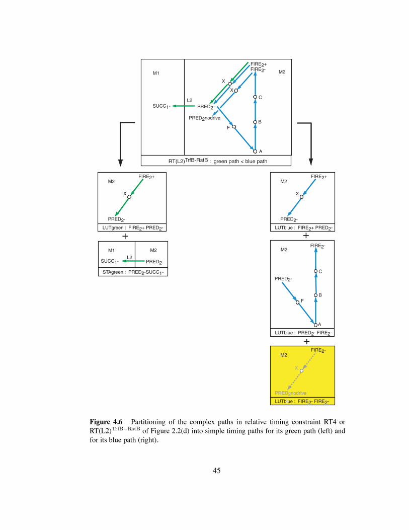
L2
STAgreen : PRED2-SUCC1-
M1 M2
+
M1
PRED2-
PRED2nodrive
FIRE2+FIRE2-
A
B
C
X
SUCC1-
X
F
RT(L2)TrfB-RstB : green path < blue path
L2
M2
FIRE2+
PRED2-
PRED2-
X
FIRE2-
A
B
C
F
LUTblue : FIRE2+ PRED2-
LUTblue : PRED2- FIRE2-
M2
FIRE2-
LUTblue : FIRE2- FIRE2-
M2
FIRE2+
PRED2-
X
LUTgreen : FIRE2+ PRED2-
M2
M2
+
+
PRED2-SUCC1-
PREDPRED2nodrivenodrive
X
Figure 4.6 Partitioning of the complex paths in relative timing constraint RT4 orRT(L2)TrfB!RstB of Figure 2.2(d) into simple timing paths for its green path (left) andfor its blue path (right).
45
This concludes the explanation of the partition for RT1 in Figure 4.3. The partitionings
for RT2 to RT4 in Figure 4.4 to 4.6 follow the same approach — specifically:
• Path names for each of the simple paths include information about path color,
namely red or green or blue, and about how the information is captured, namely
by look up table (LUT) or via static timing analysis (STA). So, by looking at the
path name we will know how to set up the path simulations for delays and slopes.
Green and red paths will be simulated for maximum delays. Blue paths will be
simulated for minimum delays. That way, we can easily validate RT1 to RT4,
which are all of one of the two following forms:
% the total red path delay is less than the total blue path delay, or
% the total green path delay is less than the total blue path delay.
• Each blue path partition ends in a final path with a nodrive target. The final blue
path in Figure 4.4 ends in SUCC1nodrive. The final blue paths in Figure 4.5 and
Figure 4.6 end in PRED2nodrive. As in Figure 4.3, we approximate these targets
by observing the input signal to the drive transistor: instead of SUCC1nodrive we
observe Dout1, and instead of PRED2nodrive we observe FIRE2. As before, we
emphasize this in the graph by changing the path line and arrow color from solid
blue to dashed grey for the indirect observation part.
• The final graphs for the paths with nodrive target PRED2nodrive in Figure 4.5
and Figure 4.6 have a yellow background to indicate that something special is
happening here. Both paths start when signal FIRE2 reaches a pre-determined
output voltage level in the previous path and they end when FIRE2 drops below
the threshold level of drive transistor X. We will not distinguish these two points.
In other words: we declare the paths in the yellow-colored graphs of Figure 4.5
and Figure 4.6 empty and will delete these paths from the RT3 and RT4 partitions.
46
4.4 STEP 2: Defining an Accurate Simulation Set-Up for Simple Paths
In Section 4.4, we will create accurate simulation set-ups for the input-to-output delay
and slope calculations of the simple paths for RT1 to RT4. We will do this as follows.
Using the complex to simple path partitions for RT1 to RT4 in Figure 4.3 to Figure 4.6
of Section 4.3, we will partition the 6-4 GasP modules M1 and M2 in Figure 2.1 into
sub-circuits that allow us to simulate and capture the input-to-output delay and slope
information for each particular simple path in RT1 to RT4. We do this in Section 4.4.1
In Section 4.4.2 we will enhance this collection of sub-circuits with extra features so we
can (1) simulate minimum and maximum delay scenarios using ‘The Charlie Effect’,
and (2) enable simulation sweeps for simple paths ending in un-driven state wires.
In Section 4.4.3 we revisit the solution approach of PART-A of Chapter 3 and show how
we can simulate this collection of enhanced sub-circuits to generate look up tables for
each simple path in RT1 to RT4 that has a name starting with ‘LUT’. We leave the paths
with names starting with ‘STA’ to static timing analysis. The look up tables will capture
the path delays and output slopes under various input slopes and output loads.
Section 4.5 shows how we can generalize the limited simulation setups that we used in
Section 4.4.3, and make them work for all possible sweep cases.
4.4.1 Circuit Partitioning for RT1 to RT4
In this section, we will partition the two-stage GasP FIFO in Figure 2.1 into sub-circuits
that act as the core simulation set-up for the simple paths of RT1–RT4 in Figures 4.3
to 4.6. So, for instance, we partition the circuit in Figure 2.1 to fit the RT1 partition in
Figure 4.3. It is not necessary that this sub-circuit partitioning matches the sub-circuit
partitioning for RT2 or RT3 or RT4, but we will try to share sub-circuits where we can,
because this will reduce the total number of simulation set-ups.
47
One way to reduce and simplify simulation set-ups is to work with input slopes, like most
of the look up table generation methods do — and to not work with input loads. There
is a strong motivation to do it this way:
• If we generate look up tables by simulating input-to-output delays and output
slopes for a range of input slopes and output loads, then it does not matter how
we obtain the input slopes. In particular: it does not matter which output loads we
used in the simulation set-up for a preceding path to generate the output slope that
we now use as input slope for the present path. As a result, the simulation set-ups
for subsequent paths are independent of each other.
• Were we to use input loads, and generate look up tables by simulating input-to-
output delays and output slopes for a range of input loads and output loads, the
dependency between the simulation set-ups of subsequent paths would make it
hard or at least more complex to share the simulation set-up between paths with
different continuations or with different previous paths.
As an example, consider the simple path LUTblue:PREDi"FIREi", which is
in the partition of RT1 in Figure 4.3 for i=1, and in the partition of RT4 in
Figure 4.6 for i=2. Given that Modules M1 and M2 use the same circuit tem-
plate, the paths are the same for i=1 and i=2. But the successor path in RT1
is LUTblue:FIREi"Douti+ and has the capacitive load of gate D on its input
FIRE1, while the successor path in RT4 is empty and thus carries no load on its
input FIRE2. Simulating the joint path LUTblue:PREDi"FIREi"with all its out-
put loads, i.e. for X and D and the VDD-connected PMOS half-keeper and the
external latches, would give the correct output delay and slope for RT4. But the
delays would be skewed for the RT1 continuation into LUTblue:FIREi"Douti+
because load D is used twice.
48
To fix this, we can either simulate the joint path twice, once for RT1 with all the
output loads, and once more for RT4 with all the output loads except for D. Or,
we can simulate the joint path for a wider range of loads to cover both simulation
set-ups in one run. For RT1 we would use the results for the look up table index
(Cin, Cout"CD) and for RT4 we would use the results at index (Cin, Cout) , where
Cin, Cout, CD are the input load capacitance at PREDi, the full load capacitance
at output FIREi, and the load capacitance of gate D.
This gets more complex when the number of successor or predecessor paths
grows. The more successor and predecessor paths there are to a joint path, the
more dependencies we will need to track and the more complex look up table
generation and usage will become. For us, this is the key motivation to generate
look up tables by using input slopes instead of input loads.
Figure 4.7 shows a complete collection of sub-circuits of Figure 2.1 for covering the
relative timing partitions of RT1, RT2, RT3 and RT4 in Figure 4.3 to Figure 4.6. The
signals in the sub-circuits of Figure 4.7 are indexed using (i " 1) and i and (i + 1)
instead of 1 for M1 and 2 for M2. The variable indexing enables us to exploit the fact
that modules M1 and M2 have identical schematics and use similar single-track wire
connections to both their predecessor and successor modules. The index variables also
make it easier to identify a shared circuit and simulation set-up for simple relative timing
paths that differ only in their index number.
49
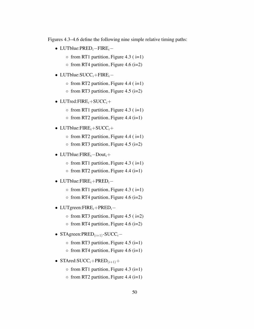
Figures 4.3–4.6 define the following nine simple relative timing paths:
• LUTblue:PREDi"FIREi"
% from RT1 partition, Figure 4.3 ( i=1)% from RT4 partition, Figure 4.6 (i=2)
• LUTblue:SUCCi+FIREi"
% from RT2 partition, Figure 4.4 ( i=1)% from RT3 partition, Figure 4.5 (i=2)
• LUTred:FIREi+SUCCi+
% from RT1 partition, Figure 4.3 ( i=1)% from RT2 partition, Figure 4.4 (i=1)
• LUTblue:FIREi+SUCCi+
% from RT2 partition, Figure 4.4 ( i=1)% from RT3 partition, Figure 4.5 (i=2)
• LUTblue:FIREi"Douti+
% from RT1 partition, Figure 4.3 ( i=1)% from RT2 partition, Figure 4.4 (i=1)
• LUTblue:FIREi+PREDi"
% from RT1 partition, Figure 4.3 ( i=1)% from RT4 partition, Figure 4.6 (i=2)
• LUTgreen:FIREi+PREDi"
% from RT3 partition, Figure 4.5 ( i=2)% from RT4 partition, Figure 4.6 (i=2)
• STAgreen:PRED(i+1)-SUCCi"
% from RT3 partition, Figure 4.5 (i=1)% from RT4 partition, Figure 4.6 (i=1)
• STAred:SUCCi+PRED(i+1)+
% from RT1 partition, Figure 4.3 (i=1)% from RT2 partition, Figure 4.4 (i=1)
50
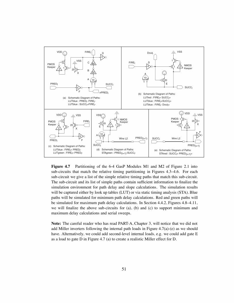
20
1
1
20
FIREi
PREDi
SUCCi
FIREi
PREDi SUCCi
FIREi
nPREDi
SUCCi
PRED(i+1)
24
5
30
80
10
F
A
B
CNMOSKeeper
X
Wire L2
LUTblue : FIREi+ PREDi-
LUTblue : PREDi- FIREi- LUTblue : FIREi- Douti+
LUTred : FIREi+ SUCCi+
STAred : SUCCi+ PRED(i+1)+
LUTblue : FIREi+SUCCi+ Schematic Diagram of Paths:
Schematic Diagram of Paths:
Schematic Diagram of Paths:Schematic Diagram of Paths:
1
12KeeperPMOS
D
E
DoutiVDD VSS
VSS
LUTgreen : FIREi+ PREDi-
PRED(i+1)
SUCCi
Wire L2
Schematic Diagram of Paths:STAgreen : PRED(i+1)-SUCCi-
10A
1
1 2
VDD
(a)
(b)
(c)(d) (e)
LUTblue : SUCCi+FIREi-
1
12
VDD
5
F
1
12
NMOSKeeper
VSS
5F
4D
20X
VSS
10
A
PMOSKeeper
PMOSKeeper
20E
20X
VSS
Figure 4.7 Partitioning of the 6-4 GasP Modules M1 and M2 of Figure 2.1 intosub-circuits that match the relative timing partitioning in Figures 4.3–4.6. For eachsub-circuit we give a list of the simple relative timing paths that match this sub-circuit.The sub-circuit and its list of simple paths contain sufficient information to finalize thesimulation environment for path delay and slope calculations. The simulation resultswill be captured either by look up tables (LUT) or via static timing analysis (STA). Bluepaths will be simulated for minimum path delay calculations. Red and green paths willbe simulated for maximum path delay calculations. In Section 4.4.2, Figures 4.8–4.11,we will finalize the above sub-circuits for (a), (b) and (c) to support minimum andmaximum delay calculations and serial sweeps.
Note: The careful reader who has read PART-A, Chapter 3, will notice that we did notadd Miller inverters following the internal path loads in Figure 4.7(a)-(e) as we shouldhave. Alternatively, we could add second-level internal loads, e.g. we could add gate Eas a load to gate D in Figure 4.7 (a) to create a realistic Miller effect for D.
51
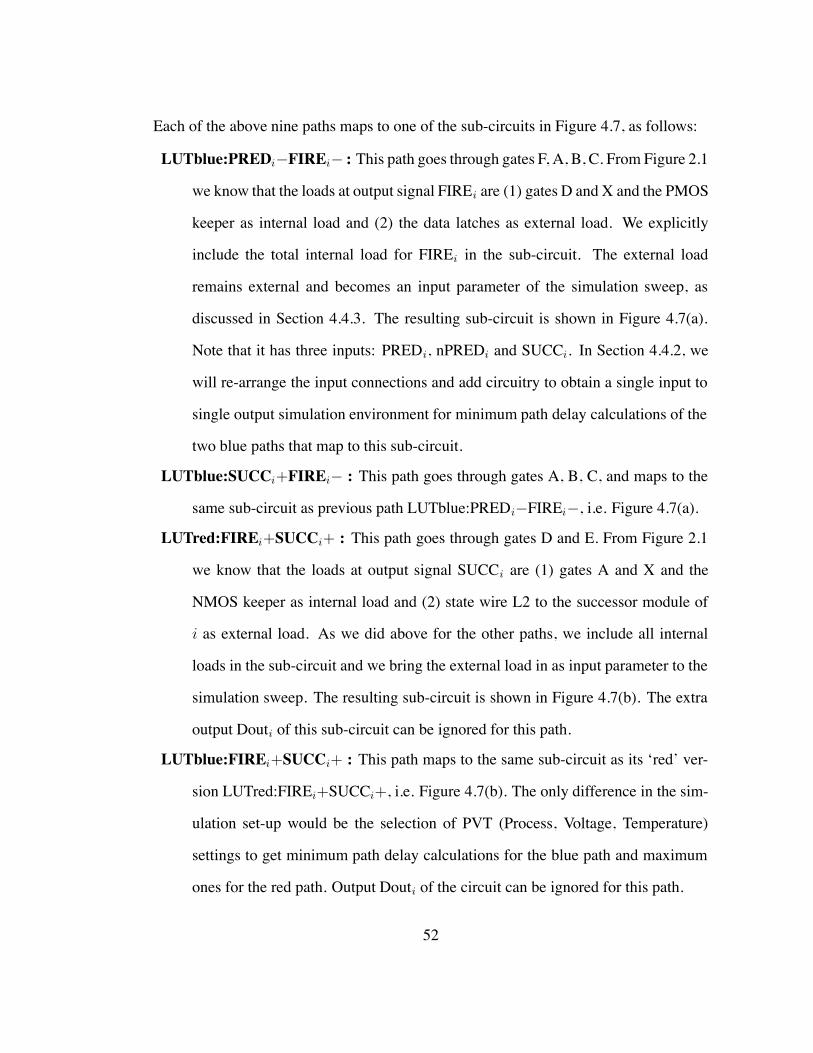
Each of the above nine paths maps to one of the sub-circuits in Figure 4.7, as follows:
LUTblue:PREDi"FIREi" : This path goes through gates F, A, B, C. From Figure 2.1
we know that the loads at output signal FIREi are (1) gates D and X and the PMOS
keeper as internal load and (2) the data latches as external load. We explicitly
include the total internal load for FIREi in the sub-circuit. The external load
remains external and becomes an input parameter of the simulation sweep, as
discussed in Section 4.4.3. The resulting sub-circuit is shown in Figure 4.7(a).
Note that it has three inputs: PREDi, nPREDi and SUCCi. In Section 4.4.2, we
will re-arrange the input connections and add circuitry to obtain a single input to
single output simulation environment for minimum path delay calculations of the
two blue paths that map to this sub-circuit.
LUTblue:SUCCi+FIREi" : This path goes through gates A, B, C, and maps to the
same sub-circuit as previous path LUTblue:PREDi"FIREi", i.e. Figure 4.7(a).
LUTred:FIREi+SUCCi+ : This path goes through gates D and E. From Figure 2.1
we know that the loads at output signal SUCCi are (1) gates A and X and the
NMOS keeper as internal load and (2) state wire L2 to the successor module of
i as external load. As we did above for the other paths, we include all internal
loads in the sub-circuit and we bring the external load in as input parameter to the
simulation sweep. The resulting sub-circuit is shown in Figure 4.7(b). The extra
output Douti of this sub-circuit can be ignored for this path.
LUTblue:FIREi+SUCCi+ : This path maps to the same sub-circuit as its ‘red’ ver-
sion LUTred:FIREi+SUCCi+, i.e. Figure 4.7(b). The only difference in the sim-
ulation set-up would be the selection of PVT (Process, Voltage, Temperature)
settings to get minimum path delay calculations for the blue path and maximum
ones for the red path. Output Douti of the circuit can be ignored for this path.
52
LUTblue:FIREi"Douti+ : This path goes through just gate D. From Figure 2.1 we
know that the internal loads at output signal Douti are gate E and the NMOS
keeper, and that there are no external loads connected to Douti. This path can be
mapped to the same sub-circuit as the previous two paths, namely Figure 4.7(b).
The extra output SUCCi of this sub-circuit can be ignored for this specific path.
LUTblue:FIREi+PREDi" : This path goes through just gate X. From Figure 2.1
we know that the loads at output signal PREDi are (1) gates X and F and the
PMOS keeper as internal load and (2) state wire L2 to the predecessor module of
i as external load. As we did above for the other paths, we include all internal
loads in the sub-circuit and we bring the external load in as input parameter to the
simulation sweep. The resulting sub-circuit is shown in Figure 4.7(c).
LUTgreen:FIREi+PREDi" : This path maps to the same sub-circuit as its ‘blue’
version LUTblue:FIREi+PREDi" above, i.e. Figure 4.7(c). The only difference
in the simulation set-up would be the selection of Process, Voltage, Temperature
(PVT) settings to obtain minimum path delay calculations for the blue path and
maximum path delay calculations for the green path.
STAgreen:PRED(i+1)"SUCCi" : This path covers the state wire connection L2 from
module M(i + 1) to Mi. From Figure 2.1 we know that the loads at output signal
SUCCi are (1) gates A, E and the NMOS keeper as internal load and (2) wire
L2 as external load. As we did above for the other paths, we include all internal
loads in the sub-circuit and we bring the external load in as input parameter to the
simulation sweep. The resulting sub-circuit is shown in Figure 4.7(d).
STAred:SUCCi+PRED(i+1)+ : This path covers the state wire connection L2 from
module M(i) to module M(i + 1). From Figure 2.1 we know that the loads at
output signal PRED(i+1) are (1) gates F and X and the PMOS keeper as internal
53
load and (2) state wire L2 as external load. As we did above for the other paths,
we include all internal loads in the sub-circuit and we bring the external load in as
input parameter to the simulation sweep. The resulting sub-circuit is Figure 4.7(e).
Note that all but the final two sub-circuits in Figure 4.7(d)-(e) are associated with paths
whose timing information goes into look up tables (LUT). The paths associated with
the final two sub-circuits will be simulated with methods available during static timing
analysis (STA), using layout information, as explained on page 39 in Section 4.3. Note
too that the two STA-based paths cross module boundaries: they go from M(i + 1) to
Mi or vice versa, whereas the LUT-based paths are confined to a single module Mi. This
makes it possible to view and validate LUT-based relative timing constraints on a mod-
ule by module basis, rather than on the state wire by state wire basis that we followed
thus far. The module based view may fit better into standard tool flows than a wire based
view. For instance, it would enable us to annotate the relative timing constraints in the
schematics description of the module, as is done in the pipeline compilation flow for
‘Click’ by Handshake Solutions [20].
This is the point where we hand over the STA-based paths to future researchers of timing
flows for GasP. The rest of Chapter 4 focuses on LUT-based paths.
54
4.4.2 Circuit Enhancements for Min-Max and Repetitive Simulations
The sub-circuits and simple relative timing paths in Figure 4.7(a)–(c) are not yet ready
for simulation with the look up table generation approach of PART-A of Chapter 3 for
the following three reasons:
1. Gate A in Figure 4.7(a) exhibits different input-to-output delays depending on the
arrival times of the transitions at its two inputs, nPREDi and SUCCi. We must
minimize the delay for gate A when we are simulating blue paths, and we must
maximize the delay for A when we are simulating red and green paths. Given that
the relative timing constraints through gate A in this report use strictly blue paths,
it suffices to set up the simulation so that the gate delay for A is minimal.
2. Figure 4.7(a) has multiple inputs. The solution presented in PART-A handles only
single input to single output look up tables.
3. Figure 4.7(b) cannot be used directly for serial simulations from FIREi to SUCCi
because output SUCCi starts to float when the pulse generator on FIREi resets the
input to low before starting the next high transition. To obtain valid input to output
delay and slope measurement, we must re-initialize the output signal to low before
starting the next high transition. Likewise, Figure 4.7(c) cannot be used directly
for sweeps that contain multiple simulation cycles from FIREi to PREDi.
Section 4.4.2.1 discusses how we can solve the issues indicated in items 1–2 above.
Section 4.4.2.2 discusses how we can solve the issues explained in item 3 above. And
Section 4.4.2.3 summarizes the new list of sub-circuits and simple relative timing paths
that we obtain after solving items 1–3 for the old list of sub-circuits in Figure 4.7(a)–(c).
We will pass the new list on to Section 4.4.3 where we generate the look up tables.
55
4.4.2.1 Simulating Minimum Gate Delays
Any AND or OR type logic will have series transistors as well as transistors in parallel.
The 6-4 GasP gate A in the sub-circuit shown in Figure 4.7(a) has two PMOS transistors
in series and two NMOS transistors in parallel. When transistors in series turn on at the
same time it takes longer to conduct current than when one of the transistors is already
turned on or turned on partially. In contrast, when transistors in parallel turn on at the
same time, current is conducted faster than when one of the transistors is already on or
partially on. We call this ‘The Charlie Effect’ [1], after the late Charles Molnar. The
result is that the delay of NOR gate A is maximal when the two input signals nPREDi
and SUCCi fall at the same time, and the delay is minimal when the two input signals
rise at the same time.
For the blue-colored relative timing paths covered by Figure 4.7(a) we are interested in
the minimal propagation time for rising input transitions on nPRED i and SUCCi. This
means that we want the rising transitions to coincide. We can force this in SPICE by
using a so-called Voltage Controlled Voltage Source (VCVS) on the two signals.
A VCVS is a fictional device — or, as Ivan Sutherland calls it in our ARC report [17]:
a ‘demon in a box’ — that (or according to Ivan “who”) can be used in a simulation
environment to achieve perfectly synchronized transitions. In this case: it enables us to
generate perfectly synchronized rising transitions on gate A inputs nPREDi and SUCCi.
The VCVS in Figure 4.8 has two ports that relate to nPREDi, namely in and GNDin, and
two ports that relate to SUCCi, namely out and GNDout. It copies the voltage difference
between in and GNDin onto out and GNDout — and it does this without delay, i.e.
instantaneously.
56
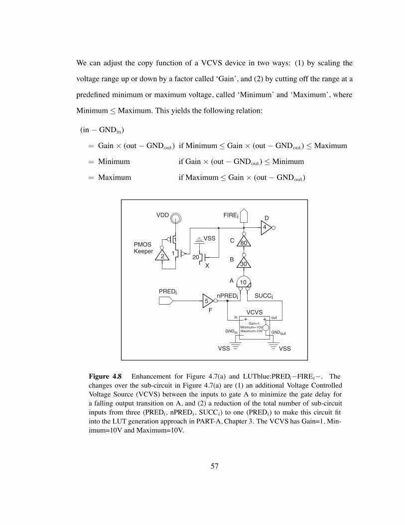
We can adjust the copy function of a VCVS device in two ways: (1) by scaling the
voltage range up or down by a factor called ‘Gain’, and (2) by cutting off the range at a
predefined minimum or maximum voltage, called ‘Minimum’ and ‘Maximum’, where
Minimum&Maximum. This yields the following relation:
(in " GNDin)
= Gain # (out " GNDout) if Minimum& Gain # (out " GNDout) &Maximum
= Minimum if Gain # (out " GNDout) &Minimum
= Maximum if Maximum& Gain # (out " GNDout)
++Gain=1
Maximum=10VMinimum=-10V
VCVS
PREDi SUCCi
FIREi
nPREDi5
30
80
10
F
A
B
C1
12KeeperPMOS
VDD
4D
20X
VSS
in out
GNDin GNDout
VSS VSS
Figure 4.8 Enhancement for Figure 4.7(a) and LUTblue:PREDi"FIREi". Thechanges over the sub-circuit in Figure 4.7(a) are (1) an additional Voltage ControlledVoltage Source (VCVS) between the inputs to gate A to minimize the gate delay fora falling output transition on A, and (2) a reduction of the total number of sub-circuitinputs from three (PREDi, nPREDi, SUCCi) to one (PREDi) to make this circuit fitinto the LUT generation approach in PART-A, Chapter 3. The VCVS has Gain=1, Min-imum=10V and Maximum=10V.
57
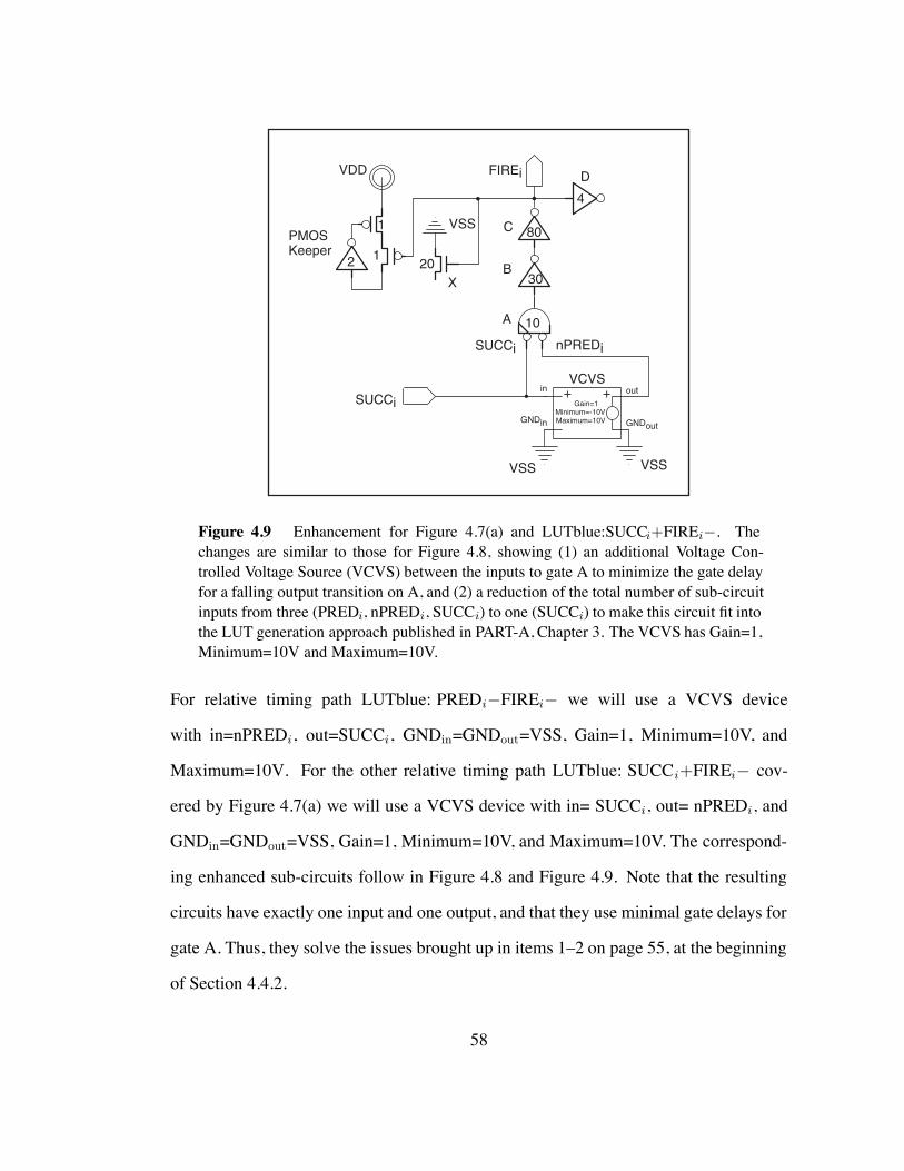
10A
SUCCi nPREDi
SUCCi
FIREi
30
80
B
C1
12KeeperPMOS
VDD
4
D
20X
VSS
++Gain=1
Maximum=10VMinimum=-10V
VCVSin out
GNDin GNDout
VSSVSS
Figure 4.9 Enhancement for Figure 4.7(a) and LUTblue:SUCCi+FIREi". Thechanges are similar to those for Figure 4.8, showing (1) an additional Voltage Con-trolled Voltage Source (VCVS) between the inputs to gate A to minimize the gate delayfor a falling output transition on A, and (2) a reduction of the total number of sub-circuitinputs from three (PREDi, nPREDi, SUCCi) to one (SUCCi) to make this circuit fit intothe LUT generation approach published in PART-A, Chapter 3. The VCVS has Gain=1,Minimum=10V and Maximum=10V.
For relative timing path LUTblue: PREDi"FIREi" we will use a VCVS device
with in=nPREDi, out=SUCCi, GNDin=GNDout=VSS, Gain=1, Minimum=10V, and
Maximum=10V. For the other relative timing path LUTblue: SUCCi+FIREi" cov-
ered by Figure 4.7(a) we will use a VCVS device with in= SUCCi, out= nPREDi, and
GNDin=GNDout=VSS, Gain=1, Minimum=10V, and Maximum=10V. The correspond-
ing enhanced sub-circuits follow in Figure 4.8 and Figure 4.9. Note that the resulting
circuits have exactly one input and one output, and that they use minimal gate delays for
gate A. Thus, they solve the issues brought up in items 1–2 on page 55, at the beginning
of Section 4.4.2.
58
4.4.2.2 Autonomously Re-Initializing Un-Driven Wires
The GasP family communicates bi-directionally over single-track state wires between
modules. A module connected to a state wire can either raise the wire or lower the wire,
but it cannot do both. For instance, module M1 in Figure 2.1, page 11, can raise state
wire L2 via its local pull-up transistor E, and module M2 can lower L2 via its local pull-
down transistor X. In between these active pull-up and pull-down events, that each last
for about five gate delays, the state of the wire is maintained by the keepers. For state
wire L2 in Figure 2.1, the pull-up and pull-down circuit of its keeper are partitioned over
the two modules: L2-pull-up module M1 gets the maintain-low-state or NMOS keeper,
and L2-pull-downmoduleM2 gets the maintain-high-state or PMOS keeper. As a result,
the sub-circuits in Figure 4.7(b)-(c) miss half of the L2 keeper circuitry. Missing half of
the keeper circuitry turns out not to be an issue for the simulation setup. In fact, it will
turn out that the sub-circuits have exactly the right half-keeper to make the setup work.
The issue is that Figure 4.7(b) can pull SUCCi high and keep it low, but it cannot actively
lower SUCCi. This is a problem if we want to simulate more than one input-to-output
transition: a high input pulse on FIREi will initially pull SUCCi high but then leave
SUCCi un-driven and hence floating as soon as FIREi is low. If we fail to reset SUCCi
back to VSS, the next simulation will start with SUCCi at an unknown voltage level and
thereby render the simulated path delay and output slope for LUTred:FIREi+SUCCi+
and LUTblue:FIREi+SUCCi+ meaningless.4.1 This is a problem because we typically
run a few simulation cycles before we start measuring the timing, to get past initializa-
tion issues. To support multiple simulation cycles, we must reset SUCC i to its initial
state after completion of the current simulation and before the start of the next.4.1Even if module M1 had a full L2 keeper, leaving SUCC i at a stable high voltage at the end of the
FIREi pulse, we would still have to reset SUCCi to its initialization state before the next simulation cycle.
59
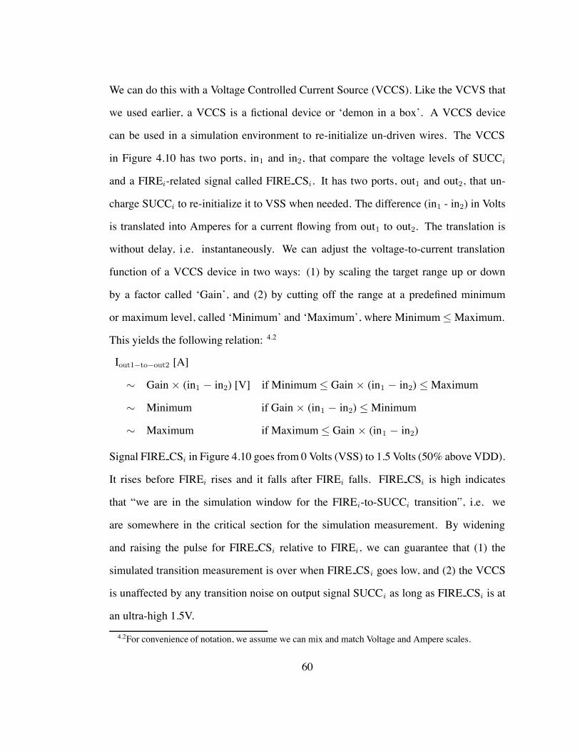
We can do this with a Voltage Controlled Current Source (VCCS). Like the VCVS that
we used earlier, a VCCS is a fictional device or ‘demon in a box’. A VCCS device
can be used in a simulation environment to re-initialize un-driven wires. The VCCS
in Figure 4.10 has two ports, in1 and in2, that compare the voltage levels of SUCCi
and a FIREi-related signal called FIRE CSi. It has two ports, out1 and out2, that un-
charge SUCCi to re-initialize it to VSS when needed. The difference (in1 - in2) in Volts
is translated into Amperes for a current flowing from out1 to out2. The translation is
without delay, i.e. instantaneously. We can adjust the voltage-to-current translation
function of a VCCS device in two ways: (1) by scaling the target range up or down
by a factor called ‘Gain’, and (2) by cutting off the range at a predefined minimum
or maximum level, called ‘Minimum’ and ‘Maximum’, where Minimum&Maximum.
This yields the following relation: 4.2
Iout1!to!out2 [A]
' Gain # (in1 " in2) [V] if Minimum& Gain # (in1 " in2) &Maximum
' Minimum if Gain # (in1 " in2) &Minimum
' Maximum if Maximum& Gain # (in1 " in2)
Signal FIRE CSi in Figure 4.10 goes from 0 Volts (VSS) to 1.5 Volts (50% above VDD).
It rises before FIREi rises and it falls after FIREi falls. FIRE CSi is high indicates
that “we are in the simulation window for the FIREi-to-SUCCi transition”, i.e. we
are somewhere in the critical section for the simulation measurement. By widening
and raising the pulse for FIRE CSi relative to FIREi, we can guarantee that (1) the
simulated transition measurement is over when FIRE CSi goes low, and (2) the VCCS
is unaffected by any transition noise on output signal SUCCi as long as FIRE CSi is at
an ultra-high 1.5V.
4.2For convenience of notation, we assume we can mix and match Voltage and Ampere scales.
60
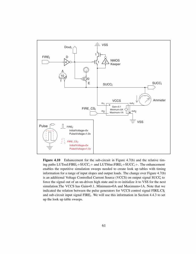
+Gain=0.1
Maximum=1AMinimum=0A
VCCS Ammeter
SUCCi
1
1
20SUCCi
FIREi24 NMOS
Keeper
D
E
DoutiVSS
10
A
in1 out1
in2 out2
VSS
FIRE_CSi
Pulse
PulseVoltage=1.0v
FIREi:
FIRE_CSi:
InitialVoltage=0v
PulseVoltage=1.5vInitialVoltage=0v
Figure 4.10 Enhancement for the sub-circuit in Figure 4.7(b) and the relative tim-ing paths LUTred:FIREi+SUCCi+ and LUTblue:FIREi+SUCCi+. The enhancementenables the repetitive simulation sweeps needed to create look up tables with timinginformation for a range of input slopes and output loads. The change over Figure 4.7(b)is an additional Voltage Controlled Current Source (VCCS) on output signal SUCCi toforce the signal out of an un-driven high state and to re-initialize it to VSS for the nextsimulation.The VCCS has Gain=0.1, Minimum=0A and Maximum=1A. Note that weindicated the relation between the pulse generators for VCCS control signal FIRE CSiand sub-circuit input signal FIREi. We will use this information in Section 4.4.3 to setup the look up table sweeps.
61
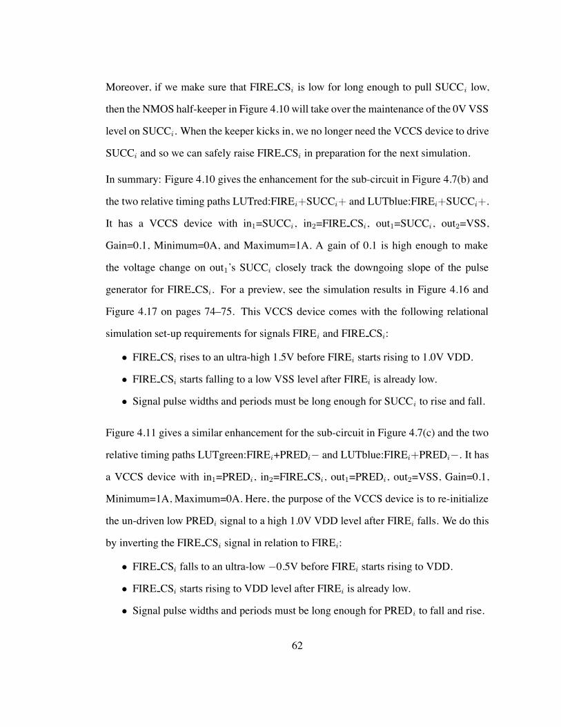
Moreover, if we make sure that FIRE CSi is low for long enough to pull SUCCi low,
then the NMOS half-keeper in Figure 4.10 will take over the maintenance of the 0V VSS
level on SUCCi. When the keeper kicks in, we no longer need the VCCS device to drive
SUCCi and so we can safely raise FIRE CSi in preparation for the next simulation.
In summary: Figure 4.10 gives the enhancement for the sub-circuit in Figure 4.7(b) and
the two relative timing paths LUTred:FIREi+SUCCi+ and LUTblue:FIREi+SUCCi+.
It has a VCCS device with in1=SUCCi, in2=FIRE CSi, out1=SUCCi, out2=VSS,
Gain=0.1, Minimum=0A, and Maximum=1A. A gain of 0.1 is high enough to make
the voltage change on out1’s SUCCi closely track the downgoing slope of the pulse
generator for FIRE CSi. For a preview, see the simulation results in Figure 4.16 and
Figure 4.17 on pages 74–75. This VCCS device comes with the following relational
simulation set-up requirements for signals FIREi and FIRE CSi:
• FIRE CSi rises to an ultra-high 1.5V before FIREi starts rising to 1.0V VDD.
• FIRE CSi starts falling to a low VSS level after FIREi is already low.
• Signal pulse widths and periods must be long enough for SUCCi to rise and fall.
Figure 4.11 gives a similar enhancement for the sub-circuit in Figure 4.7(c) and the two
relative timing paths LUTgreen:FIREi+PREDi" and LUTblue:FIREi+PREDi". It has
a VCCS device with in1=PREDi, in2=FIRE CSi, out1=PREDi, out2=VSS, Gain=0.1,
Minimum=1A, Maximum=0A. Here, the purpose of the VCCS device is to re-initialize
the un-driven low PREDi signal to a high 1.0V VDD level after FIREi falls. We do this
by inverting the FIRE CSi signal in relation to FIREi:
• FIRE CSi falls to an ultra-low "0.5V before FIREi starts rising to VDD.
• FIRE CSi starts rising to VDD level after FIREi is already low.
• Signal pulse widths and periods must be long enough for PREDi to fall and rise.
62
+Gain=0.1
Maximum=0AMinimum=-1A
AmmeterVCCS
20
FIREi
PREDi
X
VSS
1
1 2
VDD
5F
PMOSKeeper
in1 out1
in2 out2FIRE_CSi
Pulse
PulseVoltage=1.0v
FIREi:
FIRE_CSi:
InitialVoltage=0v
PulseVoltage=-0.5vInitialVoltage=1.0v
VSS
Figure 4.11 Enhancement for the sub-circuit in Figure 4.7(c) and relative timingsLUTblue:FIREi+PREDi" and LUTgreen:FIREi+PREDi" to enable the repetitivesimulation sweeps needed to create look up tables with timing information for a rangeof input slopes and output loads. The enhancement is similar to Figure 4.10. It uses anadditional Voltage Controlled Current Source (VCCS) on output signal PREDi to forcethe signal out of an undriven low state and to re-initialize it to VDD for the next simula-tion. The VCCS device has Gain=0.1, Minimum=1A and Maximum=0A. Note that weindicated the relation between the pulse generators for VCCS control signal FIRE CSiand sub-circuit input signal FIREi. We will use this information in Section 4.4.3 to setup the look up table sweeps.
63
The VCCS in Figure 4.11 translates a negative voltage difference (PREDi " FIRE CSi)
into a negative current Iout1!to!out2 in the range of 1A to 0A. This corresponds to a
positive current flow in the range of 0A to 1A from out2 to out1, i.e. to PREDi, which
charges PREDi until the voltage on PREDi matches that of VDD. Note that this works
independent of the actual voltage source for out2 —out2 can be VSS or VDD or"200V.
What matters is the out2-to-out1 direction of the current flow and the gain. A gain of 0.1
is high enough to make the voltage change on out1’s PREDi closely track the upgoing
slope of the pulse generator for FIRE CSi. For a quick preview, see the simulation
results in Figure 4.19 and Figure 4.20 on pages 79–80.
Note that both Figure 4.10 and Figure 4.11 have an Ampere meter to measure
Iout1!to!out2. We use the Ampere meter to validate that the VCCS operation does not
interfere with the actual simulation measurement. We will come back to this again in
Sections 4.4.3.4–4.4.3.5.
4.4.2.3 Summary of Circuit Enhancements
The new list of sub-circuits and simple relative timing paths that we get by solving the
issues on page 55 for the old sub-circuits in Figure 4.7(a)–(c) on page 51 is as follows:
1. Figure 4.8, replacing Figure 4.7(a), with LUTblue:PREDi"FIREi"
2. Figure 4.9, replacing Figure 4.7(a), with LUTblue:SUCCi+FIREi"
3. Figure 4.7(b) with LUTblue:FIREi" Douti+
4. Figure 4.10, replacing Figure 4.7(b), with LUTred/blue:FIREi+SUCCi+
5. Figure 4.11, replacing Figure 4.7(c), with LUTblue/green:FIREi+PREDi"
We will pass this list on to Section 4.4.3 where we generate the look up tables.
64

4.4.3 Back to PART-A to Generate Look Up Tables
In this section, we will take the sub-circuits and simple relative timing paths listed in
the previous Section 4.4.2.3 and build the final simulation environments to generate
look up tables with timing information on input-to-output delay and output slope, for a
range of input slopes and output load conditions. To build the look up table simulation
environments, we follow the procedure explained in PART-A, Chapter 3, which can be
summarized as follows:
• To create realistic input slopes, we use a so-called driver inverter at the input of the
sub-circuit. We sweep the input slope by sweeping the size of the driver inverter.
To simulate a range of driver sizes, we use a pulse generator with a pulse width
and period that are long enough for the path transition to complete and stabilize.
We add a so-called source inverter between pulse generator and driver inverter to
provide realistic input slopes to the driver inverter. The source inverter is a step-up
of 3 smaller than the driver inverter.
• To create realistic output loads, we use a so-called load inverter. We sweep the
capacitive output load by sweeping the size of the load inverter. We add a so-
called Miller inverter at the output of the load inverter for a realistic Miller effect.
The Miller inverter is a step-up of 3 larger than the load inverter.
In our sweeps, we maintain a relationship between driving and driven inverters where
the size of the driving inverter is 0.20 (1/5th) to 2 times the size of the gate that it drives.
This makes sense from a design perspective. In summary: we sweep the driver inverter
from 0.20 to 2 times the size of the sub-circuit gate that it drives, and we sweep the
load inverter from 0.5 (1/2nd) to 5 times the size of the sub-circuit gate that drives it.
We use wids, wid1, wid2, widM to denote the size of respectively the source inverter,
65

the driver inverter, the load inverter, and the Miller inverter. We maintain a step-up of 3
size relationship between the source inverter and the driver inverter. This means that we
sweep both inverters simultaneously, using the current wid1 value for the driver inverter
and wids=(wid1)/3 for the source inverter. Similarly, we use widM=3#wid2.
In the following five Sections 4.4.3.1–4.4.3.5, we prepare the final look up table simula-
tion sweep for each of the five sub-circuit-with-simple-paths listed in Section 4.4.2.3.
4.4.3.1 Setup for Figure 4.8 and LUTblue:PREDi"FIREi"
Figure 4.12 shows the simulation setup for the sub-circuit in Figure 4.8 and simple rel-
ative timing path LUTblue:PREDi"FIREi". The sub-circuit and path are represented
by a black box. Only the information that we need from the black box is visible:
• Input PREDi and output FIREi, as these connect to the simulation environment.
• Size of initial gate in the path, i.e. 5 (for F), and of final gate, i.e. 80 (for C), as
these determine the sweep sizes for the source, driver, load, Miller inverters.
• Path name, LUTblue:PREDi"FIREi", because this specifies the transition type
(input/output rising/falling, fast/slow).
The sweep values for source, driver, load, Miller inverters are calculated as follows:
• Size wid1 of the driver inverter has a sweep range from 0.2#F to 2#F, where F=5
— the size of the first black box gate in the path. We divided this 1-10 range into
five more-or-less linear integer sizes, giving wid1=1, 3, 6, 8, 10.
• Size wids for the source is a step down of 3 the size of the driver inverter, wid1.
For now, we exclude wid1=1 from our sweep, because it would yield a size for
wids below the minimum inverter size of 1. In Section 4.5, we will give a general
solution for obtaining a step down of 3 with buildable inverter sizes, i.e. inverter
sizes (1. For now, the sweep values for wids are: 1, 2, 3, 3.
66
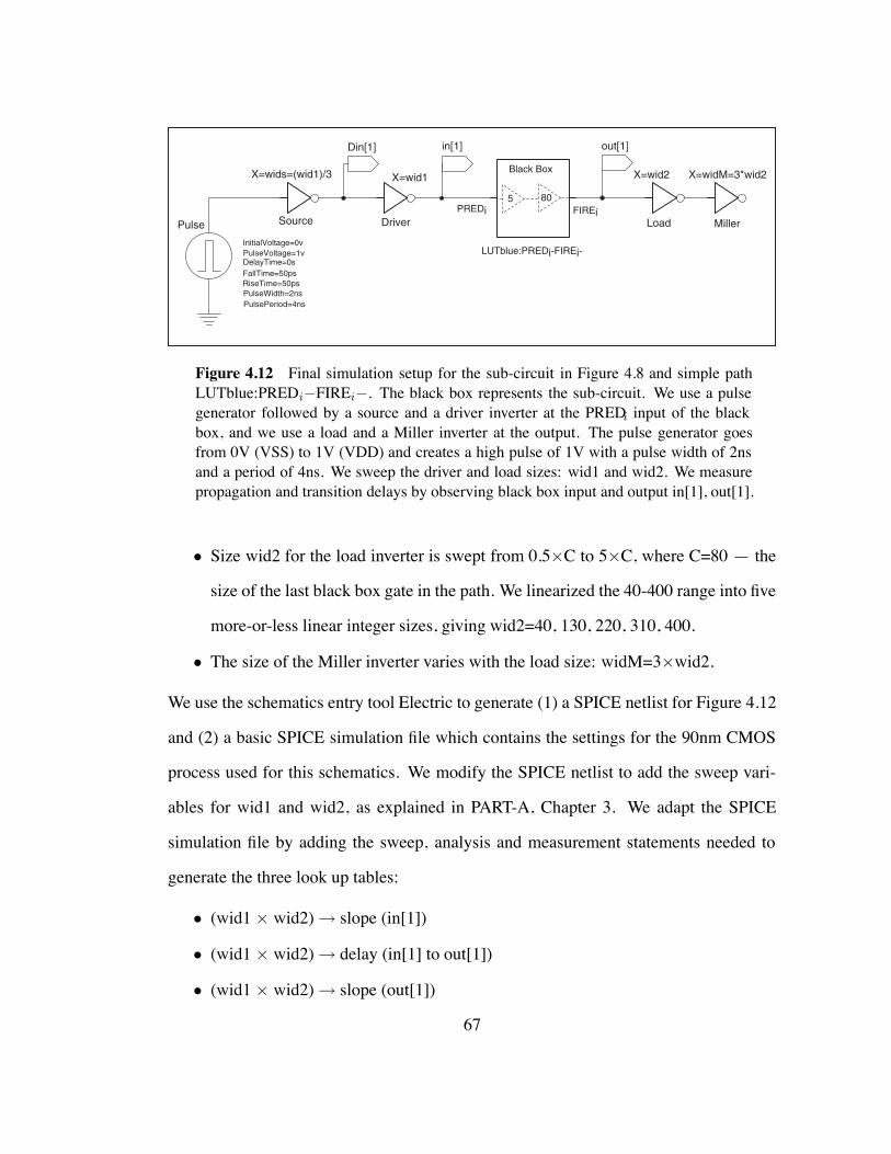
X=wids=(wid1)/3 X=wid1
Din[1] in[1]
Driver SourcePulse
out[1]
X=wid2 X=widM=3*wid2
PREDi FIREiLoad Miller
Black Box
5 80
LUTblue:PREDi-FIREi-
FallTime=50ps
InitialVoltage=0vPulseVoltage=1v
PulseWidth=2nsRiseTime=50ps
DelayTime=0s
PulsePeriod=4ns
Figure 4.12 Final simulation setup for the sub-circuit in Figure 4.8 and simple pathLUTblue:PREDi"FIREi". The black box represents the sub-circuit. We use a pulsegenerator followed by a source and a driver inverter at the PREDi input of the blackbox, and we use a load and a Miller inverter at the output. The pulse generator goesfrom 0V (VSS) to 1V (VDD) and creates a high pulse of 1V with a pulse width of 2nsand a period of 4ns. We sweep the driver and load sizes: wid1 and wid2. We measurepropagation and transition delays by observing black box input and output in[1], out[1].
• Size wid2 for the load inverter is swept from 0.5#C to 5#C, where C=80 — the
size of the last black box gate in the path. We linearized the 40-400 range into five
more-or-less linear integer sizes, giving wid2=40, 130, 220, 310, 400.
• The size of the Miller inverter varies with the load size: widM=3#wid2.
We use the schematics entry tool Electric to generate (1) a SPICE netlist for Figure 4.12
and (2) a basic SPICE simulation file which contains the settings for the 90nm CMOS
process used for this schematics. We modify the SPICE netlist to add the sweep vari-
ables for wid1 and wid2, as explained in PART-A, Chapter 3. We adapt the SPICE
simulation file by adding the sweep, analysis and measurement statements needed to
generate the three look up tables:
• (wid1 # wid2)$ slope (in[1])
• (wid1 # wid2)$ delay (in[1] to out[1])
• (wid1 # wid2)$ slope (out[1])
67

SPICE netlist, simulation, and result files are shown in Appendix C. We have used typ-
ical Process, Voltage and Temperature (PVT) library settings, here. In general, though,
we would advise using fast settings to characterize blue paths, because we are interested
in minimum delays for blue paths.
4.4.3.2 Setup for Figure 4.9 and LUTblue:SUCCi+FIREi"
Figure 4.13 shows the simulation setup for the sub-circuit in Figure 4.9 and simple rel-
ative timing path LUTblue:SUCCi+FIREi". The sub-circuit and path are represented
by a black box. Only the information that we need from the black box is visible:
• Input SUCCi and output FIREi, as these connect to the simulation environment.
• Size of initial gate 4.3 in the path, i.e. 10 (for A), and of final gate, i.e. 80 (for C),
as these determine the sweep sizes for the source, driver, load, Miller inverters.
• Path name, LUTblue:SUCCi+FIREi", because this specifies the transition type
(input/output rising/falling, fast/slow).
The sweep values for source, driver, load, Miller inverters are calculated in the same
way as we calculated the sweep values for the previous Figure 4.12 in Section 4.4.3.1:
• Driver sweep values for wid1 are: 2 (=0.20#10), 6, 10, 16, 20 (=2#10).
• Source sweep values for wids are a step down of 3 from the size of the driver
inverter, wid1. As in Section 4.4.3.1, we exclude wid1=2 from our sweep, because
it yields a size for wids below the minimum inverter size of 1. In Section 4.5, we
show how this can be solved. For now, the sweep values for wids are: 1, 2, 3, 3.
• load sweep values for wid2 are: 40 (=0.5#80), 130, 220, 310, 400 (=5#80).
• The size of the Miller inverter varies with the load size: widM=3#wid2.
4.3We simplified this calculation. The real size seen by the driver is 10#(LogicalEffort(A) def= 5/3)'17.
68
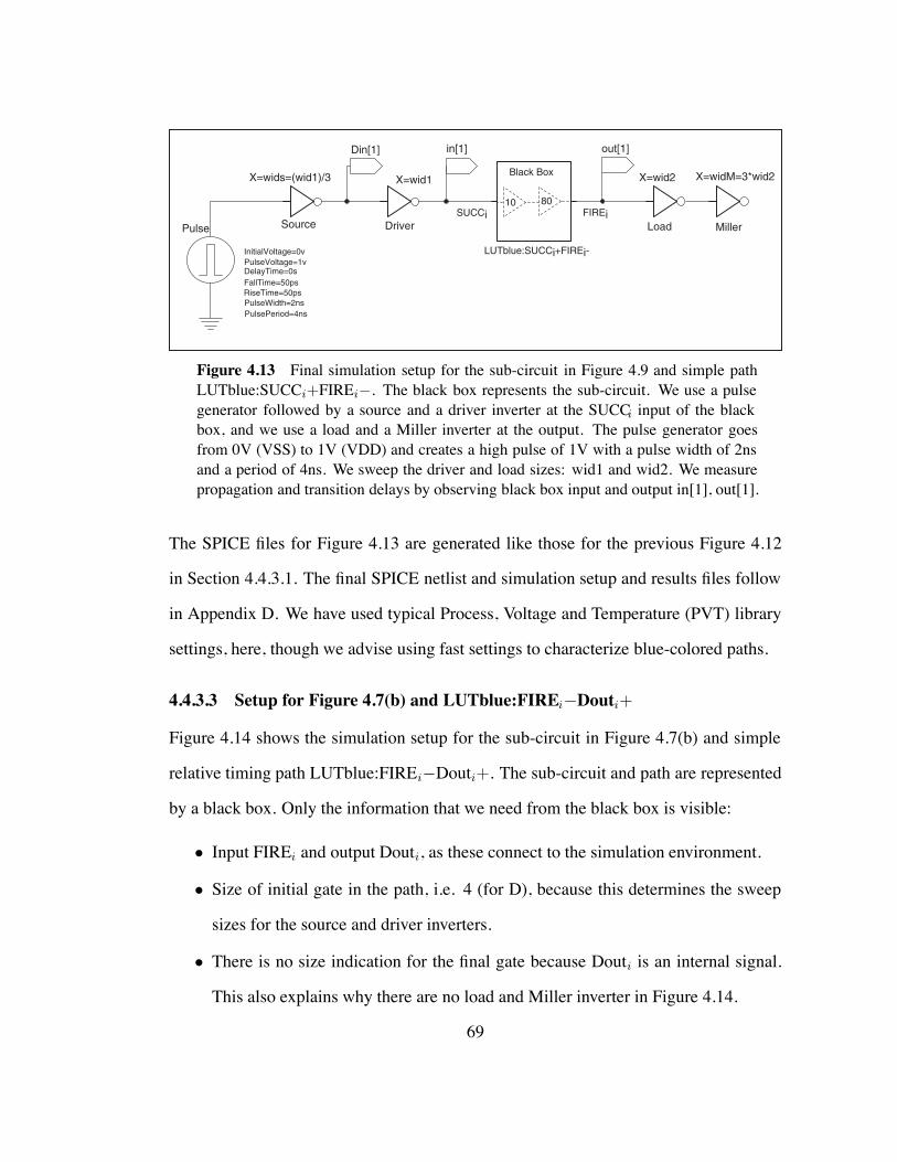
X=wid1
Din[1] in[1]
Driver SourcePulse
LUTblue:SUCCi+FIREi-
out[1]
X=wid2
SUCCi FIREiLoad Miller
Black Box
10 80
FallTime=50ps
InitialVoltage=0vPulseVoltage=1v
PulseWidth=2nsRiseTime=50ps
DelayTime=0s
PulsePeriod=4ns
X=wids=(wid1)/3 X=widM=3*wid2
Figure 4.13 Final simulation setup for the sub-circuit in Figure 4.9 and simple pathLUTblue:SUCCi+FIREi". The black box represents the sub-circuit. We use a pulsegenerator followed by a source and a driver inverter at the SUCCi input of the blackbox, and we use a load and a Miller inverter at the output. The pulse generator goesfrom 0V (VSS) to 1V (VDD) and creates a high pulse of 1V with a pulse width of 2nsand a period of 4ns. We sweep the driver and load sizes: wid1 and wid2. We measurepropagation and transition delays by observing black box input and output in[1], out[1].
The SPICE files for Figure 4.13 are generated like those for the previous Figure 4.12
in Section 4.4.3.1. The final SPICE netlist and simulation setup and results files follow
in Appendix D. We have used typical Process, Voltage and Temperature (PVT) library
settings, here, though we advise using fast settings to characterize blue-colored paths.
4.4.3.3 Setup for Figure 4.7(b) and LUTblue:FIREi"Douti+
Figure 4.14 shows the simulation setup for the sub-circuit in Figure 4.7(b) and simple
relative timing path LUTblue:FIREi"Douti+. The sub-circuit and path are represented
by a black box. Only the information that we need from the black box is visible:
• Input FIREi and output Douti, as these connect to the simulation environment.
• Size of initial gate in the path, i.e. 4 (for D), because this determines the sweep
sizes for the source and driver inverters.
• There is no size indication for the final gate because Douti is an internal signal.
This also explains why there are no load and Miller inverter in Figure 4.14.
69
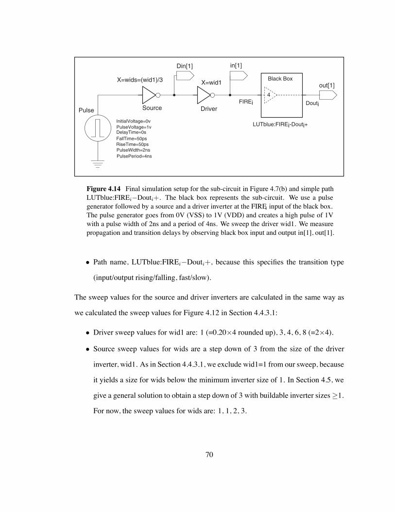
X=wid1
Din[1] in[1]
Driver SourcePulse
LUTblue:FIREi-Douti+
out[1]
FIREi Douti
Black Box
4
FallTime=50ps
InitialVoltage=0vPulseVoltage=1v
PulseWidth=2nsRiseTime=50ps
DelayTime=0s
PulsePeriod=4ns
X=wids=(wid1)/3
Figure 4.14 Final simulation setup for the sub-circuit in Figure 4.7(b) and simple pathLUTblue:FIREi"Douti+. The black box represents the sub-circuit. We use a pulsegenerator followed by a source and a driver inverter at the FIREi input of the black box.The pulse generator goes from 0V (VSS) to 1V (VDD) and creates a high pulse of 1Vwith a pulse width of 2ns and a period of 4ns. We sweep the driver wid1. We measurepropagation and transition delays by observing black box input and output in[1], out[1].
• Path name, LUTblue:FIREi"Douti+, because this specifies the transition type
(input/output rising/falling, fast/slow).
The sweep values for the source and driver inverters are calculated in the same way as
we calculated the sweep values for Figure 4.12 in Section 4.4.3.1:
• Driver sweep values for wid1 are: 1 (=0.20#4 rounded up), 3, 4, 6, 8 (=2#4).
• Source sweep values for wids are a step down of 3 from the size of the driver
inverter, wid1. As in Section 4.4.3.1, we exclude wid1=1 from our sweep, because
it yields a size for wids below the minimum inverter size of 1. In Section 4.5, we
give a general solution to obtain a step down of 3 with buildable inverter sizes(1.
For now, the sweep values for wids are: 1, 1, 2, 3.
70

The SPICE files for Figure 4.14 are generated like those for Figure 4.12 in Sec-
tion 4.4.3.1 and follow in Appendix E. We have used typical Process, Voltage and
Temperature (PVT) library settings. In general, we would advise using fast settings to
characterize blue paths, because we are interested in minimum delays for blue paths.
4.4.3.4 Setup for Figure 4.10, LUTred/blue:FIREi+SUCCi+
Figure 4.15 shows the simulation setup for the sub-circuit in Figure 4.10 and simple
relative timing paths LUTred:FIREi+SUCCi+ and LUTblue:FIREi+SUCCi+. Sub-
circuit and paths are represented by a black box. Only the information that we need
from the black box is visible:
• Input FIREi and output SUCCi, as these connect to the simulation environment.
• Size of initial gate in the paths, i.e. 4 (for D), and of final gate, i.e. 20 (for E), as
these determine the sweep sizes for the source, driver, load, Miller inverters.
• Path names LUTred:FIREi+SUCCi+ and LUTblue:FIREi+SUCCi+, because
these specify the transition type (input/output rising/falling, fast/slow).
• Pulse generator for VCCS input FIRE CSi, because it must be aligned to FIREi.
• Ampere meter monitoring the VCCS current flow for Iout1!to!out2 to validate that
the VCCS operation does not interfere with the actual simulation measurement.
The sweep values for source, driver, load, Miller inverters are calculated in the same
way as we calculated the sweep values for Figure 4.12 in Section 4.4.3.1:
• Driver sweep values for wid1 are: 1 (=0.20#4 rounded up), 3, 4, 6, 8 (=2#4).
• Source sweep values for wids are a step down of 3 from the size of the driver
inverter, wid1. As in Section 4.4.3.1, we exclude wid1=1 from our sweep, because
it yields a size for wids below the minimum inverter size of 1. In Section 4.5, we
give a general solution to obtain a step down of 3 with buildable inverter sizes(1.
For now, the sweep values for wids are: 1, 1, 2, 3.
71
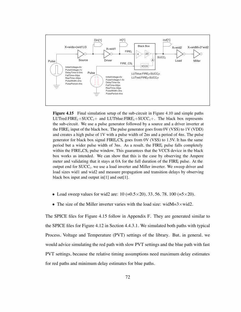
X=wid1
Din[1] in[1]
Driver SourcePulse
LUTblue:FIREi+SUCCi+
out[1]
X=wid2
SUCCi
FIREi
Load Miller
LUTred:FIREi+SUCCi+
Black Box
A
20
FallTime=50ps
InitialVoltage=0vPulseVoltage=1v
PulseWidth=2nsRiseTime=50ps
DelayTime=0.5ns
PulsePeriod=4ns
X=wids=(wid1)/3 X=widM=3*wid2
FIRE_CSi
Pulse
FallTime=50ps
InitialVoltage=0vPulseVoltage=1.5v
PulseWidth=3nsRiseTime=50ps
DelayTime=0s
PulsePeriod=4ns
VCCS
4
Figure 4.15 Final simulation setup of the sub-circuit in Figure 4.10 and simple pathsLUTred:FIREi+SUCCi+ and LUTblue:FIREi+SUCCi+. The black box representsthe sub-circuit. We use a pulse generator followed by a source and a driver inverter atthe FIREi input of the black box. The pulse generator goes from 0V (VSS) to 1V (VDD)and creates a high pulse of 1V with a pulse width of 2ns and a period of 4ns. The pulsegenerator for black box signal FIRE CSi goes from 0V (VSS) to 1.5V. It has the sameperiod but a wider pulse width of 3ns. As a result, the FIREi pulse falls completelywithin the FIRE CSi pulse window. This guarantees that the VCCS device in the blackbox works as intended. We can show that this is the case by observing the Amperemeter and validating that it stays at 0A for the full duration of the FIREi pulse. At theoutput end for SUCCi, we use a load inverter and Miller inverter. We sweep driver andload sizes wid1 and wid2 and measure propagation and transition delays by observingblack box input and output in[1] and out[1].
• Load sweep values for wid2 are: 10 (=0.5#20), 33, 56, 78, 100 (=5#20).
• The size of the Miller inverter varies with the load size: widM=3#wid2.
The SPICE files for Figure 4.15 follow in Appendix F. They are generated similar to
the SPICE files for Figure 4.12 in Section 4.4.3.1. We simulated both paths with typical
Process, Voltage and Temperature (PVT) settings of the library. But, in general, we
would advice simulating the red path with slow PVT settings and the blue path with fast
PVT settings, because the relative timing assumptions need maximum delay estimates
for red paths and minimum delay estimates for blue paths.
72
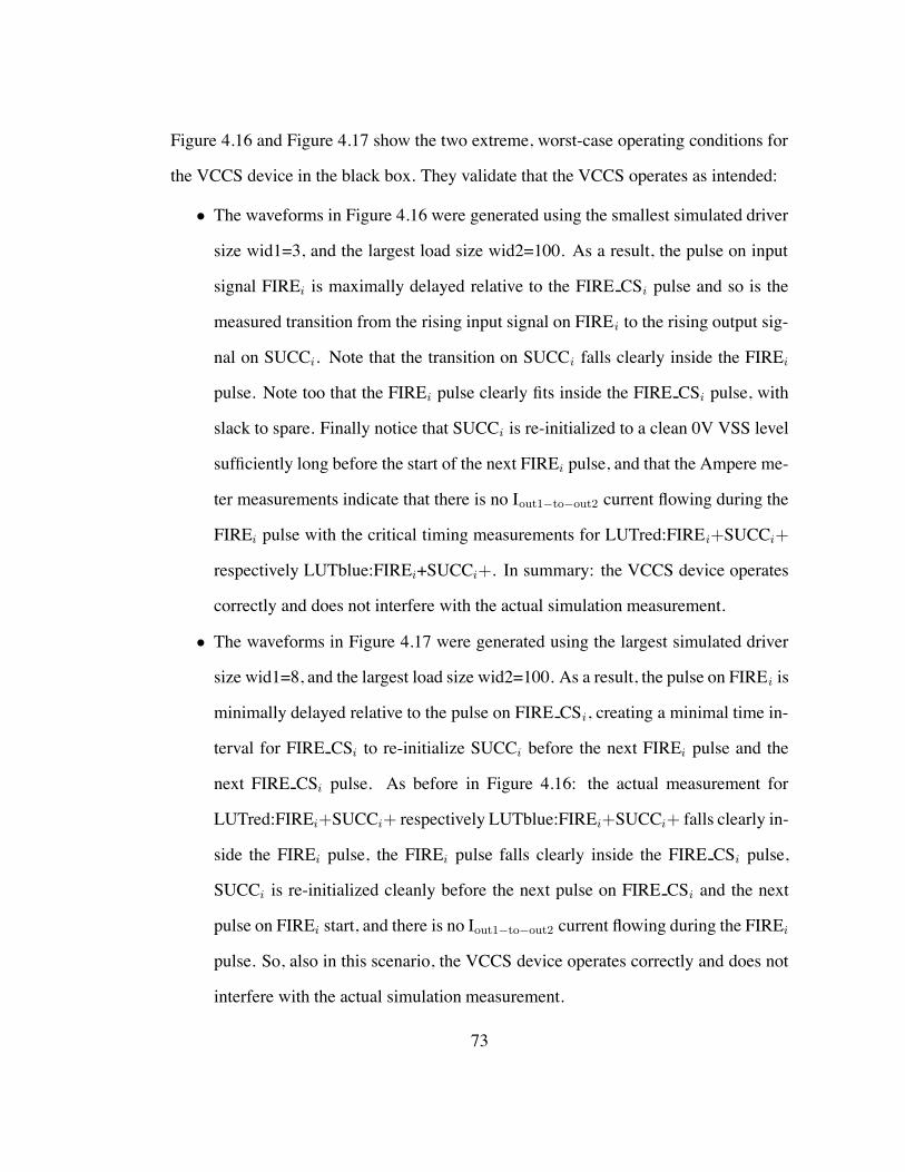
Figure 4.16 and Figure 4.17 show the two extreme, worst-case operating conditions for
the VCCS device in the black box. They validate that the VCCS operates as intended:
• The waveforms in Figure 4.16 were generated using the smallest simulated driver
size wid1=3, and the largest load size wid2=100. As a result, the pulse on input
signal FIREi is maximally delayed relative to the FIRE CSi pulse and so is the
measured transition from the rising input signal on FIREi to the rising output sig-
nal on SUCCi. Note that the transition on SUCCi falls clearly inside the FIREi
pulse. Note too that the FIREi pulse clearly fits inside the FIRE CSi pulse, with
slack to spare. Finally notice that SUCCi is re-initialized to a clean 0V VSS level
sufficiently long before the start of the next FIREi pulse, and that the Ampere me-
ter measurements indicate that there is no Iout1!to!out2 current flowing during the
FIREi pulse with the critical timing measurements for LUTred:FIREi+SUCCi+
respectively LUTblue:FIREi+SUCCi+. In summary: the VCCS device operates
correctly and does not interfere with the actual simulation measurement.
• The waveforms in Figure 4.17 were generated using the largest simulated driver
size wid1=8, and the largest load size wid2=100. As a result, the pulse on FIREi is
minimally delayed relative to the pulse on FIRE CSi, creating a minimal time in-
terval for FIRE CSi to re-initialize SUCCi before the next FIREi pulse and the
next FIRE CSi pulse. As before in Figure 4.16: the actual measurement for
LUTred:FIREi+SUCCi+ respectively LUTblue:FIREi+SUCCi+ falls clearly in-
side the FIREi pulse, the FIREi pulse falls clearly inside the FIRE CSi pulse,
SUCCi is re-initialized cleanly before the next pulse on FIRE CSi and the next
pulse on FIREi start, and there is no Iout1!to!out2 current flowing during the FIREi
pulse. So, also in this scenario, the VCCS device operates correctly and does not
interfere with the actual simulation measurement.
73
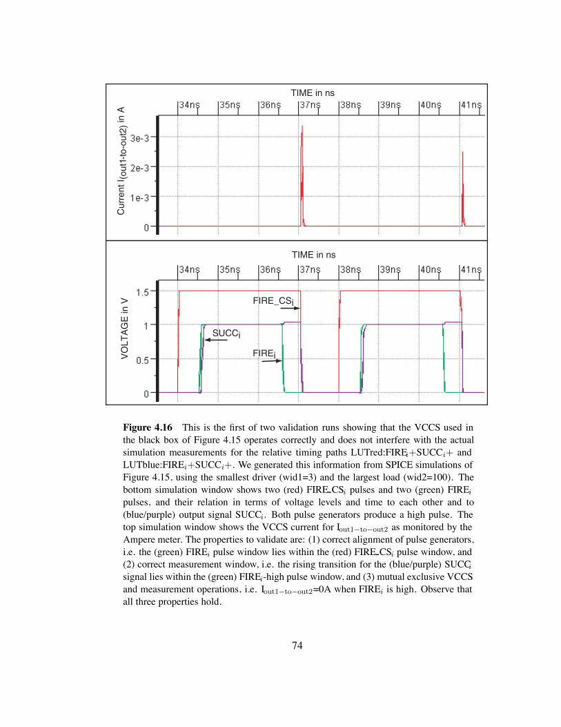
SUCCi
FIREi
TIME in ns
VO
LTA
GE
in V
TIME in ns
FIRE_CSi
Cur
rent
I (ou
t1-to
-out
2) in
A
Figure 4.16 This is the first of two validation runs showing that the VCCS used inthe black box of Figure 4.15 operates correctly and does not interfere with the actualsimulation measurements for the relative timing paths LUTred:FIREi+SUCCi+ andLUTblue:FIREi+SUCCi+. We generated this information from SPICE simulations ofFigure 4.15, using the smallest driver (wid1=3) and the largest load (wid2=100). Thebottom simulation window shows two (red) FIRE CSi pulses and two (green) FIREi
pulses, and their relation in terms of voltage levels and time to each other and to(blue/purple) output signal SUCCi. Both pulse generators produce a high pulse. Thetop simulation window shows the VCCS current for Iout1!to!out2 as monitored by theAmpere meter. The properties to validate are: (1) correct alignment of pulse generators,i.e. the (green) FIREi pulse window lies within the (red) FIRE CSi pulse window, and(2) correct measurement window, i.e. the rising transition for the (blue/purple) SUCCisignal lies within the (green) FIREi-high pulse window, and (3) mutual exclusive VCCSand measurement operations, i.e. Iout1!to!out2=0A when FIREi is high. Observe thatall three properties hold.
74
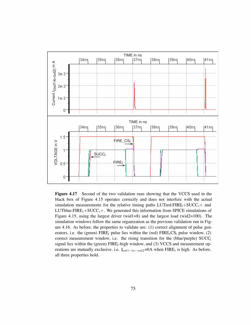
SUCCi
FIREi
TIME in ns
VO
LTA
GE
in V
TIME in ns
FIRE_CSi
Cur
rent
I (ou
t1-to
-out
2) in
A
Figure 4.17 Second of the two validation runs showing that the VCCS used in theblack box of Figure 4.15 operates correctly and does not interfere with the actualsimulation measurements for the relative timing paths LUTred:FIREi+SUCCi+ andLUTblue:FIREi+SUCCi+. We generated this information from SPICE simulations ofFigure 4.15, using the largest driver (wid1=8) and the largest load (wid2=100). Thesimulation windows follow the same organization as the previous validation run in Fig-ure 4.16. As before, the properties to validate are: (1) correct alignment of pulse gen-erators, i.e. the (green) FIREi pulse lies within the (red) FIRE CSi pulse window, (2)correct measurement window, i.e. the rising transition for the (blue/purple) SUCCisignal lies within the (green) FIREi-high window, and (3) VCCS and measurement op-erations are mutually exclusive, i.e. Iout1!to!out2=0A when FIREi is high. As before,all three properties hold.
75
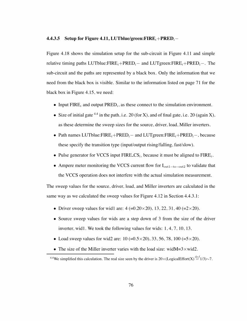
4.4.3.5 Setup for Figure 4.11, LUTblue/green:FIREi+PREDi"
Figure 4.18 shows the simulation setup for the sub-circuit in Figure 4.11 and simple
relative timing paths LUTblue:FIREi+PREDi" and LUTgreen:FIREi+PREDi". The
sub-circuit and the paths are represented by a black box. Only the information that we
need from the black box is visible. Similar to the information listed on page 71 for the
black box in Figure 4.15, we need:
• Input FIREi and output PREDi, as these connect to the simulation environment.
• Size of initial gate 4.4 in the path, i.e. 20 (for X), and of final gate, i.e. 20 (again X),
as these determine the sweep sizes for the source, driver, load, Miller inverters.
• Path names LUTblue:FIREi+PREDi" and LUTgreen:FIREi+PREDi", because
these specify the transition type (input/output rising/falling, fast/slow).
• Pulse generator for VCCS input FIRE CSi, because it must be aligned to FIREi.
• Ampere meter monitoring the VCCS current flow for Iout1!to!out2 to validate that
the VCCS operation does not interfere with the actual simulation measurement.
The sweep values for the source, driver, load, and Miller inverters are calculated in the
same way as we calculated the sweep values for Figure 4.12 in Section 4.4.3.1:
• Driver sweep values for wid1 are: 4 (=0.20#20), 13, 22, 31, 40 (=2#20).
• Source sweep values for wids are a step down of 3 from the size of the driver
inverter, wid1. We took the following values for wids: 1, 4, 7, 10, 13.
• Load sweep values for wid2 are: 10 (=0.5#20), 33, 56, 78, 100 (=5#20).
• The size of the Miller inverter varies with the load size: widM=3#wid2.4.4We simplified this calculation. The real size seen by the driver is 20#(LogicalEffort(X) def= 1/3)'7.
76
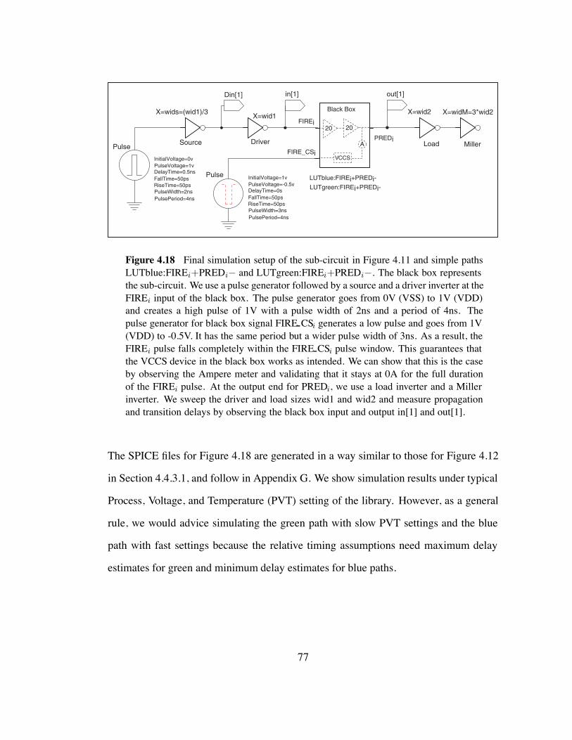
X=wid1
Din[1] in[1]
Driver SourcePulse
LUTblue:FIREi+PREDi-
out[1]
X=wid2
PREDi
FIREi
Load Miller
LUTgreen:FIREi+PREDi-
Black Box
20 20
FallTime=50ps
InitialVoltage=0vPulseVoltage=1v
PulseWidth=2nsRiseTime=50ps
DelayTime=0.5ns
PulsePeriod=4ns
FIRE_CSi
Pulse
FallTime=50ps
InitialVoltage=1vPulseVoltage=-0.5v
PulseWidth=3nsRiseTime=50ps
DelayTime=0s
PulsePeriod=4ns
X=wids=(wid1)/3 X=widM=3*wid2
VCCS
A
Figure 4.18 Final simulation setup of the sub-circuit in Figure 4.11 and simple pathsLUTblue:FIREi+PREDi" and LUTgreen:FIREi+PREDi". The black box representsthe sub-circuit. We use a pulse generator followed by a source and a driver inverter at theFIREi input of the black box. The pulse generator goes from 0V (VSS) to 1V (VDD)and creates a high pulse of 1V with a pulse width of 2ns and a period of 4ns. Thepulse generator for black box signal FIRE CSi generates a low pulse and goes from 1V(VDD) to -0.5V. It has the same period but a wider pulse width of 3ns. As a result, theFIREi pulse falls completely within the FIRE CSi pulse window. This guarantees thatthe VCCS device in the black box works as intended. We can show that this is the caseby observing the Ampere meter and validating that it stays at 0A for the full durationof the FIREi pulse. At the output end for PREDi, we use a load inverter and a Millerinverter. We sweep the driver and load sizes wid1 and wid2 and measure propagationand transition delays by observing the black box input and output in[1] and out[1].
The SPICE files for Figure 4.18 are generated in a way similar to those for Figure 4.12
in Section 4.4.3.1, and follow in Appendix G. We show simulation results under typical
Process, Voltage, and Temperature (PVT) setting of the library. However, as a general
rule, we would advice simulating the green path with slow PVT settings and the blue
path with fast settings because the relative timing assumptions need maximum delay
estimates for green and minimum delay estimates for blue paths.
77
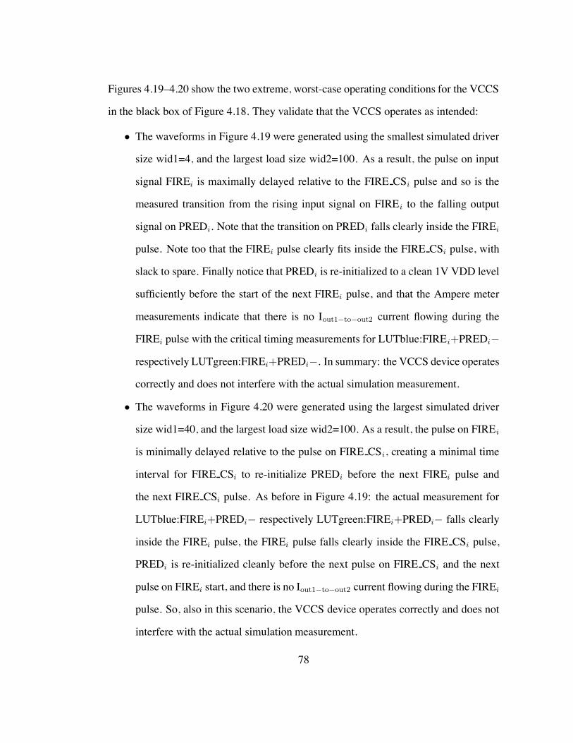
Figures 4.19–4.20 show the two extreme, worst-case operating conditions for the VCCS
in the black box of Figure 4.18. They validate that the VCCS operates as intended:
• The waveforms in Figure 4.19 were generated using the smallest simulated driver
size wid1=4, and the largest load size wid2=100. As a result, the pulse on input
signal FIREi is maximally delayed relative to the FIRE CSi pulse and so is the
measured transition from the rising input signal on FIREi to the falling output
signal on PREDi. Note that the transition on PREDi falls clearly inside the FIREi
pulse. Note too that the FIREi pulse clearly fits inside the FIRE CSi pulse, with
slack to spare. Finally notice that PREDi is re-initialized to a clean 1V VDD level
sufficiently before the start of the next FIREi pulse, and that the Ampere meter
measurements indicate that there is no Iout1!to!out2 current flowing during the
FIREi pulse with the critical timing measurements for LUTblue:FIREi+PREDi"
respectively LUTgreen:FIREi+PREDi". In summary: the VCCS device operates
correctly and does not interfere with the actual simulation measurement.
• The waveforms in Figure 4.20 were generated using the largest simulated driver
size wid1=40, and the largest load size wid2=100. As a result, the pulse on FIREi
is minimally delayed relative to the pulse on FIRE CSi, creating a minimal time
interval for FIRE CSi to re-initialize PREDi before the next FIREi pulse and
the next FIRE CSi pulse. As before in Figure 4.19: the actual measurement for
LUTblue:FIREi+PREDi" respectively LUTgreen:FIREi+PREDi" falls clearly
inside the FIREi pulse, the FIREi pulse falls clearly inside the FIRE CSi pulse,
PREDi is re-initialized cleanly before the next pulse on FIRE CSi and the next
pulse on FIREi start, and there is no Iout1!to!out2 current flowing during the FIREi
pulse. So, also in this scenario, the VCCS device operates correctly and does not
interfere with the actual simulation measurement.
78
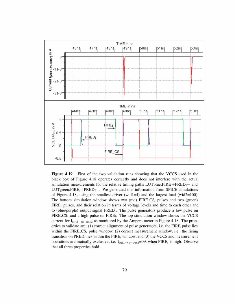
PREDi
FIREi
TIME in ns
VO
LTA
GE
in V
TIME in ns
FIRE_CSi
Cur
rent
I (ou
t1-to
-out
2) in
A
Figure 4.19 First of the two validation runs showing that the VCCS used in theblack box of Figure 4.18 operates correctly and does not interfere with the actualsimulation measurements for the relative timing paths LUTblue:FIREi+PREDi" andLUTgreen:FIREi+PREDi". We generated this information from SPICE simulationsof Figure 4.18, using the smallest driver (wid1=4) and the largest load (wid2=100).The bottom simulation window shows two (red) FIRE CSi pulses and two (green)FIREi pulses, and their relation in terms of voltage levels and time to each other andto (blue/purple) output signal PREDi. The pulse generators produce a low pulse onFIRE CSi and a high pulse on FIREi. The top simulation window shows the VCCScurrent for Iout1!to!out2 as monitored by the Ampere meter in Figure 4.18. The prop-erties to validate are: (1) correct alignment of pulse generators, i.e. the FIREi pulse lieswithin the FIRE CSi pulse window, (2) correct measurement window, i.e. the risingtransition on PREDi lies within the FIREi window, and (3) the VCCS and measurementoperations are mutually exclusive, i.e. Iout1!to!out2=0A when FIREi is high. Observethat all three properties hold.
79
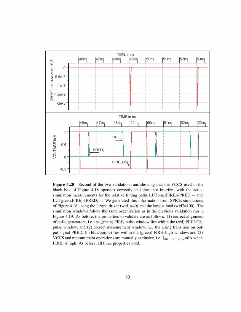
PREDi
FIREi
TIME in ns
VO
LTA
GE
in V
TIME in ns
FIRE_CSi
Cur
rent
I (ou
t1-to
-out
2) in
A
Figure 4.20 Second of the two validation runs showing that the VCCS used in theblack box of Figure 4.18 operates correctly and does not interfere with the actualsimulation measurements for the relative timing paths LUTblue:FIREi+PREDi" andLUTgreen:FIREi+PREDi". We generated this information from SPICE simulationsof Figure 4.18, using the largest driver (wid1=40) and the largest load (wid2=100). Thesimulation windows follow the same organization as in the previous validation run inFigure 4.19. As before, the properties to validate are as follows: (1) correct alignmentof pulse generators, i.e. the (green) FIREi pulse window lies within the (red) FIRE CSi
pulse window, and (2) correct measurement window, i.e. the rising transition on out-put signal PREDi (in blue/purple) lies within the (green) FIREi-high window, and (3)VCCS and measurement operations are mutually exclusive, i.e. Iout1!to!out2=0A whenFIREi is high. As before, all three properties hold.
80

4.5 General Simulation Setup Covering All Possible Sweep Cases
Section 4.5.1 below shows a simulation environment that provides arbitrary external
input drives, as weak or as strong as needed. The issue with the simulation environment
defined in PART-A, Chapter 3, is that it does not support weak input drives in the order
of 0.20 times the size of the path input gate for four out of the five relative timing paths
characterized here in PART-B, Chapter 4.
Section 4.5.2 shows how to deal with zero external output loads. We like to include zero
external output load simulations to obtain lowerbounds for path propagation delays and
output slopes.
4.5.1 Covering All Possible External Input Drives
The first four out of five simulation setups, namely those described in Section 4.4.3.1 to
Section 4.4.3.4, lack the smallest-size driver. Only the fifth simulation setup described
in Section 4.4.3.5, contains the full sweep range. We defined the smallest driver size
to be 0.20 times the size of the first gate on the relative timing path that we plan to
simulate, rounded off to the closest integer greater or equal to 1, with 1 being the size
of the minimum inverter for the CMOS process of the design – see the introduction of
Section 4.4.3 on page 65. The reason for deleting the smallest-size driver from the first
four simulation setups is not because the driver size is too small, but because the extra
source inverter that we insert between the pulse generator and the driver is too small.
We require a step up of 3 in size between the source and driver, to ensure that the
driver receives a realistic input slope, independent of the slope of the pulse generator.
The smallest source inverter that we can build in this process has size wids=1. The
smallest driver size wid1 that this input configuration supports is a step-up of 3 bigger,
i.e. wid1=3#wids=3. To support a sweep value of 0.2, a driver size wid1=3 will support
81
X=wid1=100*widBB
in[1]
Driver Source
Pulse
out[1]
X=wid2
Load Miller2
Din[1] X=widT
X=widM1=3*widTMiller1
Trash
Black Box
out
FallTime=50ps
InitialVoltage=0vPulseVoltage=1v
PulseWidth=2nsRiseTime=50ps
DelayTime=0s
PulsePeriod=4ns
X=wids=(100/3)*widBB X=widM2=3*wid2
widBBin out
Figure 4.21 General simulation setup for look up table sweeps, ignoring potentialVCVS and VCCS add-ons. We sweep widT to set the input slope at in[1], and wesweep wid2 to set the capacitive output load at out[1]. Note that we fixed driver andsource sizes to wid1=100#widBB and wids=(100/3)#widBB.
a smallest first gate size widBB=wid1/0.2=15 for the first gate of the timed path. The
fifth configuration in Figure 4.18, page 77 has size widBB=20(15, and so the fifth
configuration can support the complete sweep. But the first four simulation setups all
have widBB&10, which explains why we cannot support the complete sweep. We can
solve this issue, and support complete sweeps for any input gate size widBB(1 by using
a slightly different input configuration.
Figure 4.21 shows the new simulation setup. The new setup adds two inverters to the
original input setup: a so-called Trash inverter and its Miller inverter, called Miller1.
Note that we renamed the Miller inverter at the output to Miller2. The Trash inverter
and its Miller inverter are inserted as extra load for the driver inverter, in addition to
the black box. The result will be that the driver output is divided over the two loads as
follows:
• Valsweep = (widBB + widT)/wid1, where widT is the size of the Trash inverter.
82
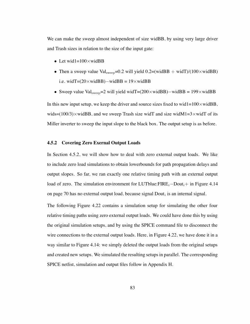
We can make the sweep almost independent of size widBB, by using very large driver
and Trash sizes in relation to the size of the input gate:
• Let wid1=100#widBB
• Then a sweep value Valsweep=0.2 will yield 0.2=(widBB + widT)/(100#widBB)
i.e. widT=(20#widBB)"widBB = 19#widBB
• Sweep value Valsweep=2 will yield widT=(200#widBB)"widBB = 199#widBB
In this new input setup, we keep the driver and source sizes fixed to wid1=100#widBB,
wids=(100/3)#widBB, and we sweep Trash size widT and size widM1=3#widT of its
Miller inverter to sweep the input slope to the black box. The output setup is as before.
4.5.2 Covering Zero Exernal Output Loads
In Section 4.5.2, we will show how to deal with zero external output loads. We like
to include zero load simulations to obtain lowerbounds for path propagation delays and
output slopes. So far, we ran exactly one relative timing path with an external output
load of zero. The simulation environment for LUTblue:FIREi"Douti+ in Figure 4.14
on page 70 has no external output load, because signal Douti is an internal signal.
The following Figure 4.22 contains a simulation setup for simulating the other four
relative timing paths using zero external output loads. We could have done this by using
the original simulation setups, and by using the SPICE command file to disconnect the
wire connections to the external output loads. Here, in Figure 4.22, we have done it in a
way similar to Figure 4.14: we simply deleted the output loads from the original setups
and created new setups. We simulated the resulting setups in parallel. The corresponding
SPICE netlist, simulation and output files follow in Appendix H.
83
X=wids1=(widd1)/3 X=widd1
Din1 in1
Driver SourcePulse
out1
PREDi FIREi
Black Box
5 80
LUTblue:PREDi-FIREi-
FallTime=50ps
InitialVoltage=0vPulseVoltage=1v
PulseWidth=2nsRiseTime=50ps
DelayTime=0s
PulsePeriod=4ns in2
X=widd2
Din2
Driver SourcePulse
LUTblue:SUCCi+FIREi-
SUCCi FIREi
Black Box
10 80
FallTime=50ps
InitialVoltage=0vPulseVoltage=1v
PulseWidth=2nsRiseTime=50ps
DelayTime=0s
PulsePeriod=4ns
X=wids1=(widd2)/3out2
Pulse
X=widd3
Din3 in3
Driver Source
LUTblue:FIREi+SUCCi+
SUCCi
FIREi
LUTred:FIREi+SUCCi+
Black Box
A
20
FallTime=50ps
InitialVoltage=0vPulseVoltage=1v
PulseWidth=2nsRiseTime=50ps
DelayTime=0.5ns
PulsePeriod=4ns
X=wids3=(widd3)/3
FIRE_CSi
Pulse
FallTime=50ps
InitialVoltage=0vPulseVoltage=1.5v
PulseWidth=3nsRiseTime=50ps
DelayTime=0s
PulsePeriod=4ns
VCCS
4
out3
in4
X=widd4
Din4
Driver SourcePulse
LUTblue:FIREi+PREDi-
PREDi
FIREi
LUTgreen:FIREi+PREDi-
Black Box
20 20
FallTime=50ps
InitialVoltage=0vPulseVoltage=1v
PulseWidth=2nsRiseTime=50ps
DelayTime=0.5ns
PulsePeriod=4ns
FIRE_CSi
Pulse
FallTime=50ps
InitialVoltage=1vPulseVoltage=-0.5v
PulseWidth=3nsRiseTime=50ps
DelayTime=0s
PulsePeriod=4ns
X=wids4=(widd4)/3
VCCS
A
out4
Figure 4.22 Simulation setup with zero external output loads for the original setups inFigure 4.12 (top), Figure 4.13 (second), Figure 4.15 (third), and Figure 4.18 (bottom).We sweep widd1, widd2, widd3 and widd4 to set the input slope for each path input.We measure the propagation delays and slopes by observing in1 to in4 and out1 to out4.
84
4.6 Conclusion and Future Work for Chapter 4
In Chapter 4, we designed a characterization flow to generate look up tables with timing
information for a typical 6-4 GasP circuit. This chapter is dubbed ‘PART-B’ because it
is the second of a two-part study in look up table generation for 6-4 GasP. PART-A in
Chapter 3 is the first part. It shows how to characterize a simple 6-4 GasP library module
without loops and with a single input and output. PART-B extends the characterization
flow in PART-A to general 6-4 GasP circuits, by partitioning the timing behavior of a
6-4 GasP circuit into simple input-to-output transitions and simplified circuits that can
be fed back into PART-A. Not only do we show how to do this, but we actually do it: we
partition complex relative timing paths and feed the sub-paths back into PART-A. The
SPICE input and output files in Appendix C–H bear witness to this. Proof of the pudding
follows in Chapter 5 where we run the standard STA tool PrimeTime of Synopsys on
the look up tables in Appendix C–H to validate the four key relative timing constraints
in a 6-4 GasP module, listed on page 12.
Here is a summary of the key steps in PART-B:
STEP 1: Partition complex GasP paths by cutting them at module boundaries, i.e. at
PREDi, FIREi, SUCCi, and at internal signals that control the single-track wire
drive, i.e. at Douti. The names of the sub-path cuttings reflect key properties of
the paths. For instance, sub-path name ‘LUTblue:PREDi"FIREi"’ indicates that
(1) the timing information of the path will be captured in a look up table (LUT),
(2) we are interested in simulating this path with minimal delay settings (blue),
(3) the path starts with PREDi falling and ends with a falling transition on FIREi.
85
STEP 2: Set up an accurate simulation environment for each sub-path as follows:
1. From the 6-4 GasP schematics, include all the gates on the sub-path. For
all gates on the sub-path, include all the load capacitances on the gate by
including the gates and wires connected to the gate output. The resulting
circuit is a simplification of the original 6-4 GasP circuit. In particular, the
input signal goes to the first gate and nothing else, and the output signal
carries all the load that it carries in the 6-4 GasP schematics.
2. Model ‘The Charlie Effect’ needed for the sub-path, i.e. add a VCVS device
to synchronize the input transitions of a multi-input gate, or connect non-
leading gate inputs to VSS or VDD to let the leading input transition set
the gate delay. Two of the sub-paths characterized in Chapter 4 required a
VCVS device to synchronize the inputs of two-input gate A.
3. Re-initialize un-driven wires by adding a VCCS device. Four sub-paths that
we characterized in Chapter 4 required a VCCS device for this purpose.
4. Embed the resulting circuit into the simulation setup of PART-A to generate
SPICE input files and to create a SPICE output file with the look up tables.
As far as future work on PART-B goes, we have the following suggestions and hints:
1. Create wire models with near-end capacitive load and far-end delay information.
• It may be that an Elmore delay model suffices [23, 36].
2. Flow automation, also mentioned in the conclusion of PART-A, becomes even
more a necessity given the complexity of PART-A-to-B combined. Specifically:
• The path and circuit partitioning in PART-B can be simplified if we could
use pre-defined single-rail datapath designs with a fixed load on FIREi.
86

• There may be other, perhaps easier, ways to partition the circuit. We could
for instance keep the full schematics but avoid false feedback paths by split-
ting signals that act as output as well as input into separate pins, as is done
in the static timing analysis approach for 6-4 GasP in [2] and in Chapter 5.
3. Use the general simulation setup described in Section 4.5, Figure 4.21.
• Figure 4.21 guarantees a simulation environment designed according to the
theory of Logical Effort, and avoids that the transistor sizes shrink below the
minimum size of 1, as we experienced for 4 out of our 5 simulation setups.
4. Use asymmetric sweeps and add sweep values for the two extreme ends.
• Asymmetric sweeps make it easier to validate that the rows and columns of
the look up tables are correctly copied and not accidentally swapped during
the transfer process from SPICE output files to PrimeTime input files.
• Sweep values for driver size wid1 and load size wid2 below and above the
anticipated sweep range of a GasP design make outlier values more accessi-
ble and their effects more predictable.
87

Chapter 5
STATIC TIMING ANALYSIS OF 6-4 GASP USING LOOK UP TABLES
Chapter 5 is also available as internal report ARC2010-smg04 [19]. It describes how
we can use standard static timing analysis (STA) tools to validate the relative timing
constraints on which the correctness of 6-4 GasP circuits depends. We chose Synopsys
PrimeTime as the de facto STA tool standard. GasP is a non-standard circuit family
for STA tools like PrimeTime. The combinational loops in a GasP module and the
bi-directionality of the single-track communication channels between two GasP mod-
ules make GasP hard to digest for STA tools that are accustomed to clocked circuits
where such loops are restricted to state-holding elements like flipflops. To make GasP
digestible, we take the following approach:
1. We replace each GasP module by a black box in which each combinational loop is
modeled as a sequence of loop-less input-output paths whose timing information
is stored in look up tables.
2. We replace each bi-directional single-track wire by two uni-directional wires.
3. We reformulate each relative timing constraint as a data-to-data check from a
common point of divergence. We use this common point of divergence as a clock
signal. This brings our path1-to-path2 relative timing constraints into the standard
STA jargon of clock-to-(path1-versus-path2) constraints.
88
This approach was initially developed at the University of Southern California (USC)
by Mallika Prakash for asynchronous circuits from USC, Fulcrum and Silistix [21, 22]
and it was extended by Prasad Joshi, also USC, to the single-track circuit family that
we use in 6-4 GasP [2, 3]. What we add to it is (1) the use of realistic look up tables
for timing the loop-less sub-paths that make up the combinational loops in a 6-4 GasP
circuit [16, 17], and (2) additional relative timing constraints that our short to medium
to long wire studies for 6-4 GasP have identified as necessary timing constraints [18].
5.1 Introduction
The term ‘static’ in static timing analysis alludes to the fact that the timing is analyzed
in a data- or input- independent manner, and contrasts to the ‘dynamic’ or ‘simulated’
timing analysis that we used in our library characterization approach in Chapters 3–4.
Static timing analysis (STA) tends to be much faster than simulated timing analysis. It
is used to analyze large complex designs: think ‘systems’ rather than ‘circuit modules’.
The speed-up is largely due to its use of simplified delay models and to its limited ability
to incorporate signal dependencies. Our simplified delay models are look up tables,
which we generate with SPICE, using the library characterization approach described in
Chapters 3 and 4. A quick overview of techniques used in static timing analysis and a
list of references about the state of the art can be found in [25].
Chapter 5 shows how to run static timing analysis, using Synopsys PrimeTime [35].
The flow that we use comes from the University of Southern California (USC), and was
developed by Mallika Prakash and Prasad Joshi two former Master of Science students
in the research group of Professor Peter Beerel. Mallika developed an STA flow for
asynchronous circuits from USC, Fulcrum and Silistix [21, 22] and Prasad extended her
flow to the single-track circuit family that we use in 6-4 GasP [2, 3]. The value that
89
we add to the USC flow is the use of SPICED look up tables for 6-4 GasP, and the
methodology to generate these Tables.
We use static timing analysis to validate so-called ‘Relative Timing’ constraints [27, 28]
in our circuits. Relative timing constraints describe the order in which two signals must
arrive at a point of convergence. The signals typically start from a common point, the
point of divergence, and they are all of the form: ‘the delay for path A is less than the
delay for path B’. In this chapter, we will use static timing analysis to validate four rel-
ative timing constraints. These four constraints capture the key communication aspects
of single-track handshake signaling between two 6-4 GasP modules. They include the
two relative timing constraints for GasP with a lumped-capacitance single-track wire
model [4, 15]. In Chapter 4 we already characterized the timing information needed to
validate these four relative timing constraints, and we stored the information in a collec-
tion of look up tables. The search key (wid1 # wid2) that we use to index our look up
tables is different than the indexing used by PrimeTime. So, our first task is to translate
our SPICED look up tables into PrimeTime look up tables. After that, we follow the
USC static timing analysis flow for asynchronous circuits.
The resulting flow has five steps:
Step 1: Translate SPICED look up tables into PrimeTime look up tables.
Step 2: Replace each 6-4 GasP module in the (Verilog) design by a black box.
• Our black box model is slightly different than the one Prasad uses in [2].
Step 3: Create a (Liberty) library with the black box timing in look up tables.
• This requires renaming the tables to reflect the new black box pin names.
Step 4: Create a (Tcl) command file to validate the four relative timings.
Step 5: Run PrimeTime and inspect the timing reports.
90
The rest of Chapter 5 is organized as follows. Section 5.2 covers the translation of our
SPICED look up tables into PrimeTime look up tables, i.e. it covers Step 1 in our five-
step STA flow. Section 5.3 covers the black box model for the 6-4 GasP module, i.e. it
covers Step 2 in our five-step STA flow. Sections 5.4–5.6 cover the remaining Steps 3-5.
The timing results in Section 5.6 exclude single-track wire delays, because our look up
tables do not generate these. So, instead of letting PrimeTime analyze the effects that
short, medium, and long wires have on the four relative timing constraints, we will do
the analysis ourselves, using the simulation results from our short-to-medium-to-long
wire study in Appendix O and [18]. The analysis can be found in Chapter 6. Section 5.7
concludes Chapter 5. Appendices I–M contain all the files generated in Steps 1–5,
ranging from SPICED look up table translations to PrimeTime commands and timing
reports.
Note:
We postpone the comparison between our library characterization work and prior work
at USC by Mallika Prakash [21, 22] and Prasad Joshi [2, 3] to Chapter 7.
5.2 STEP 1: From SPICED to PrimeTime Look Up Tables
The look up tables that we generated in Chapter 4 store the timing information for the
relative timing paths RT1 to RT4 of Figure 2.2, using a two-dimensional search key
(wid1 # wid2). We store three types of timing information — see also page 15:
1. (wid1 # wid2)$ slope (in[1])
2. (wid1 # wid2)$ delay (in[1] to out[1])
3. (wid1 # wid2)$ slope (out[1])
where:
91
• wid1 is the size of the external gate driving path input in[1].
• wid2 is the size of the external gate driven by path output out[1].
• slope(in[1]) is the input transition slope, a.k.a. input slew time, as denoted by the
time difference (tin2"tin1) from time tin1 when a rising input transition on in[1]
passes the 20% supply voltage point to time tin2 when it passes the 80% voltage
point — and vice versa for a falling input transition.
• delay(in[1] to out[1]) is the input-to-output transition delay time (tout"tin) from
time tin when the input transition on in[1] passes the 50% supply voltage point to
time tout when the output transition on out[1] passes the 50% supply point.
• slope(out[1]) is the output transition slope, a.k.a. output slew, as for instance
denoted by the time difference (tout2 " tout1) from time tout1 when a falling
output transition on out[1] passes the 80% supply voltage point to time tout2
when it passes the 20% point — and vice versa for a rising output transition.
The two-dimensional search key (wid1 # wid2) in our look up tables is different than
the (input slope # capacitive output load) indexing key used by standard static timing
analysis tools like PrimeTime of Synopsys. We use sizing information instead of input
slopes and output loads, because it allows us to use the theory of Logical Effort [32]
in both the design and the characterization of our circuits. We feel that this brings
the characterization process closer to the designer’s world, which — in our opinion —
makes the characterization process less artificial and more realistic. To accommodate
standard STA tools, we measure the input slopes for a given drive size and we have
methods to translate a driven output size into an output load.
Section 5.2.1 shows how we translate our index key wid1 into an index for input slope.
Section 5.2.2 shows how we translate our index key wid2 into an index for output load.
Section 5.2.3 analyzes the plausibility of the resulting PrimeTime look up tables.
92
5.2.1 From Input Driver Size to Input Transition Slope
In Chapter 4 we needed a total of five look up tables to cover the loop-less sub-paths
in relative timing constraints RT1 to RT4. We refrained from generating look up tables
for the paths crossing single-track wire L2. We left the timing measurements associated
with L2 to static timing analysis (STA) with back-annotated wire information from the
final layout results. We will come back to this in Chapter 6, where we use the L2 timing
results from [18] to bring the timing information for L2 back into the STA validation for
RT1 to RT4 of Figure 2.2, page 13. We copied the five look up tables that we generated
in Chapter 4 as the top look up tables in Figure 5.3 to Figure 5.7 below.
We will use Figure 5.3 to explain the organization of each table. External driver size
wid1 acts as the column index, and size wid2 of the external load acts as the row index.
The timing information stored at table index (wid1 # wid2) is as indicated: input slope,
input-to-output delay, and output slope — all in picoseconds (ps). The numbers match
those in the SPICE output files in Appendices C–G, but we display them here with a
more realistic precision to only a tenth of a picosecond.
The middle of the three look up tables in Figure 5.3 is a translation of the top table: we
replaced column index wid1 by the average input slope produced by driver size wid1.
The calculations for the average input slope per wid1 size are shown in the top table.
We also calculated the relative difference between the average input slope and the input
slope that we measured for driver size wid1 under the various load sizes wid2. To be
precise, we calculated:
%Diff = 100 # (average-input-slope " measured-input-slope) / (average-input-slope)
93
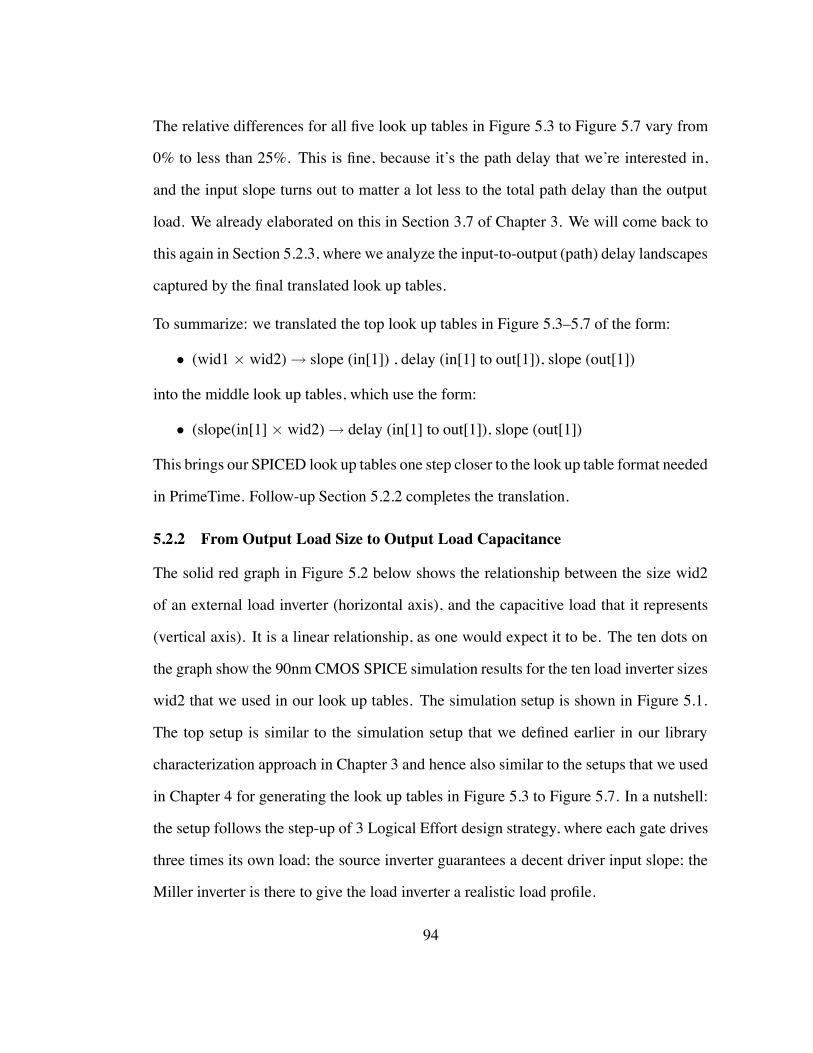
The relative differences for all five look up tables in Figure 5.3 to Figure 5.7 vary from
0% to less than 25%. This is fine, because it’s the path delay that we’re interested in,
and the input slope turns out to matter a lot less to the total path delay than the output
load. We already elaborated on this in Section 3.7 of Chapter 3. We will come back to
this again in Section 5.2.3, where we analyze the input-to-output (path) delay landscapes
captured by the final translated look up tables.
To summarize: we translated the top look up tables in Figure 5.3–5.7 of the form:
• (wid1 # wid2)$ slope (in[1]) , delay (in[1] to out[1]), slope (out[1])
into the middle look up tables, which use the form:
• (slope(in[1] # wid2)$ delay (in[1] to out[1]), slope (out[1])
This brings our SPICED look up tables one step closer to the look up table format needed
in PrimeTime. Follow-up Section 5.2.2 completes the translation.
5.2.2 From Output Load Size to Output Load Capacitance
The solid red graph in Figure 5.2 below shows the relationship between the size wid2
of an external load inverter (horizontal axis), and the capacitive load that it represents
(vertical axis). It is a linear relationship, as one would expect it to be. The ten dots on
the graph show the 90nm CMOS SPICE simulation results for the ten load inverter sizes
wid2 that we used in our look up tables. The simulation setup is shown in Figure 5.1.
The top setup is similar to the simulation setup that we defined earlier in our library
characterization approach in Chapter 3 and hence also similar to the setups that we used
in Chapter 4 for generating the look up tables in Figure 5.3 to Figure 5.7. In a nutshell:
the setup follows the step-up of 3 Logical Effort design strategy, where each gate drives
three times its own load; the source inverter guarantees a decent driver input slope; the
Miller inverter is there to give the load inverter a realistic load profile.
94
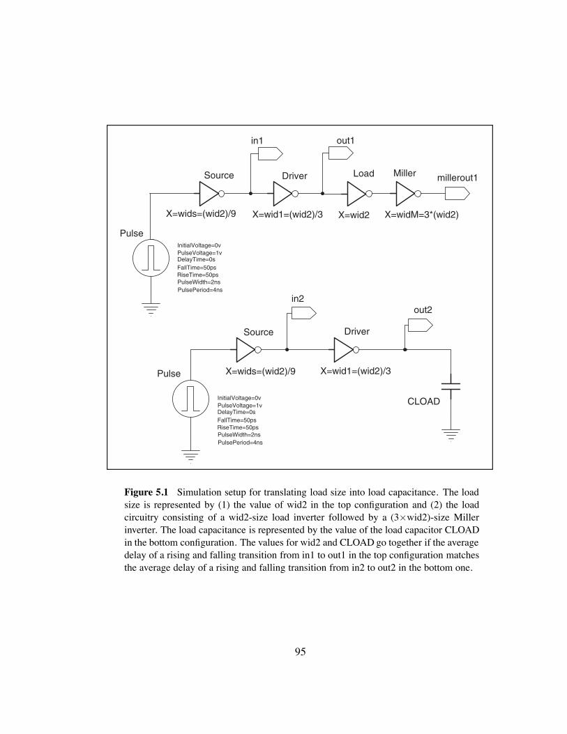
CLOAD
in1 out1
millerout1
in2out2
X=wid1=(wid2)/3X=wids=(wid2)/9 X=widM=3*(wid2)
Driver Source
Pulse
FallTime=50ps
InitialVoltage=0vPulseVoltage=1v
PulseWidth=2nsRiseTime=50ps
DelayTime=0s
PulsePeriod=4ns
Driver Source
Load
FallTime=50ps
InitialVoltage=0vPulseVoltage=1v
PulseWidth=2nsRiseTime=50ps
DelayTime=0s
PulsePeriod=4ns
Pulse X=wid1=(wid2)/3X=wids=(wid2)/9
Miller
X=wid2
Figure 5.1 Simulation setup for translating load size into load capacitance. The loadsize is represented by (1) the value of wid2 in the top configuration and (2) the loadcircuitry consisting of a wid2-size load inverter followed by a (3#wid2)-size Millerinverter. The load capacitance is represented by the value of the load capacitor CLOADin the bottom configuration. The values for wid2 and CLOAD go together if the averagedelay of a rising and falling transition from in1 to out1 in the top configuration matchesthe average delay of a rising and falling transition from in2 to out2 in the bottom one.
95

We are interested in finding the capacitive load of the wid2 load inverter in the top
schematics of Figure 5.1, for a range of sizes wid2. We find the equivalent capacitance
through a dual sweep process. First, we select a sweep value for wid2 and we measure
the average delay of a rising and falling transition from in1 to out1 through the driver
inverter. We use this average delay to start a goal-driven sweep for the bottom simula-
tion setup in Figure 5.1, where we have replaced the load circuitry by a load capacitor.
We sweep the capacitor value until we measure an average delay from in2 to out2 that
(closely) matches the average delay from in1 to out1 that we just measured for the top
simulation setup.
The SPICE netlist, simulation, and output files can be found in Appendix I. The SPICE
output file maps the ten red dots to the following (wid2 # CLOAD) values:
Size wid2 10 33 40 56 78 100 130 220 310 400
CLOAD [fF] 4.6 15.0 18.2 25.5 35.5 45.6 59.3 101.4 142.8 185.1
In addition to the red-colored solid-line graph in Figure 5.2, which we annotated with
the text ‘with Miller inverter’, there is a black-colored dotted-line graph, annotated
with the text ‘no Miller inverter’. The dotted-line graph is the result of a re-simulation
of Figure 5.1 with a top configuration that lacks a Miller inverter following the load
inverter. Without the Miller inverter, the wid2-size load inverter is perceived to have
a higher capacitive load, as one would expect, but the difference is very small for the
simulated wid2 range.
96
0.0
20.0
40.0
60.0
80.0
100.0
120.0
140.0
160.0
180.0
200.0
0 50 100 150 200 250 300 350 400
Loa
d C
apac
itan
ce
[fF]
Load Inverter size (wid2)
with Miller inverter
no Miller inverter
Figure 5.2 Graphical representation of the relationship between the size wid2 of theload inverter in the top configuration of Figure 5.1 and the load capacitance CLOADin the bottom configuration of Figure 5.1, as perceived by the driver inverter. The redsolid-line graph shows the relationship for Figure 5.1 as is. The black dotted-line graphshows the relationship for Figure 5.1 without the Miller inverter in the top configuration.
We used the red solid-line graph in Figure 5.2 to translate the look up tables in the
middle of Figure 5.3–5.7, which are of the form:
• (slope(in[1] # wid2)$ delay (in[1] to out[1]), slope (out[1])
into the bottom look up tables, which use the form:
• (slope(in[1] # cload(out[1]))$ delay (in[1] to out[1]), slope (out[1])
This completes the reformatting of our SPICED look up table for use in PrimeTime.
97
wid2 \ wid1 10 8 6 3
inputslope[ps]
% Diffto Avg
delay[ps]
outputslope[ps]
inputslope[ps]
% Diffto Avg
delay[ps]
outputslope[ps]
inputslope[ps]
% Diffto Avg
delay[ps]
outputslope[ps]
inputslope[ps]
% Diffto Avg
delay[ps]
outputslope[ps]
0 11.5 -0.9% 60.3 8.0 12.4 -2.5% 60.8 8.5 13.1 0.0% 61.1 8.3 17.9 -2.9% 63.2 8.440 11.4 0.0% 62.1 9.9 12.2 -0.8% 62.4 9.9 13.3 -1.2% 62.8 10.1 17.6 -1.1% 64.7 9.6130 11.3 0.9% 65.9 13.8 12.1 0.2% 66.1 13.8 13.4 -2.1% 66.6 13.9 17.6 -0.9% 68.3 14.0220 11.1 2.6% 69.3 18.3 11.6 4.2% 69.5 18.4 13.2 -0.4% 69.9 18.4 16.3 6.6% 71.7 18.6310 11.4 0.0% 72.3 22.7 12.2 -1.2% 72.6 22.6 12.5 5.0% 73.1 22.3 17.6 -1.4% 74.8 22.0400 11.5 -0.9% 75.1 27.1 12.2 -0.8% 75.4 27.3 13.1 0.2% 75.9 27.4 17.6 -1.0% 77.7 27.3
Averageinput slope 11.4 0.0% 12.1 0.0% 13.1 0.0% 17.4 0.0%
wid2 \ input-slope1 [ps] 11.4 12.1 13.1 17.4
delay[ps]
outputslope[ps]
delay[ps]
outputslope[ps]
delay[ps]
outputslope[ps]
delay[ps]
outputslope[ps]
0 60.3 8.0 60.8 8.5 61.1 8.3 63.2 8.440 62.1 9.9 62.4 9.9 62.8 10.1 64.7 9.6130 65.9 13.8 66.1 13.8 66.6 13.9 68.3 14.0220 69.3 18.3 69.5 18.4 69.9 18.4 71.7 18.6310 72.3 22.7 72.6 22.6 73.1 22.3 74.8 22.0400 75.1 27.1 75.4 27.3 75.9 27.4 77.7 27.3
output-load2 [fF] \ input-slope1 [ps] 11.4 12.1 13.1 17.4
delay[ps]
outputslope[ps]
delay[ps]
outputslope[ps]
delay[ps]
outputslope[ps]
delay[ps]
outputslope[ps]
0.0 60.3 8.0 60.8 8.5 61.1 8.3 63.2 8.418.2 62.1 9.9 62.4 9.9 62.8 10.1 64.7 9.659.3 65.9 13.8 66.1 13.8 66.6 13.9 68.3 14.0
101.4 69.3 18.3 69.5 18.4 69.9 18.4 71.7 18.6142.8 72.3 22.7 72.6 22.6 73.1 22.3 74.8 22.0185.1 75.1 27.1 75.4 27.3 75.9 27.4 77.7 27.3
Replace Driver size wid1 by the Average input slope that it produces
Replace Load size wid2 by its equivalent Load capacitance
LUTblue:PREDi-FIREi-
Figure 5.3 SPICE to PrimeTime look up table for LUTblue:PREDi"FIREi".
98
Replace Driver size wid1 by the Average input slope that it produces
Replace Load size wid2 by its equivalent Load capacitance
wid2 \ wid1 20 16 10 6
inputslope[ps]
% Diffto Avg
delay[ps]
outputslope[ps]
inputslope[ps]
% Diffto Avg
delay[ps]
outputslope[ps]
inputslope[ps]
% Diffto Avg
delay[ps]
outputslope[ps]
inputslope[ps]
% Diffto Avg
delay[ps]
outputslope[ps]
0 15.3 -7.7% 35.8 8.8 17.7 -17.2% 36.3 8.6 15.9 2.5% 37.4 8.5 21.7 -1.4% 39.2 8.3
40 14.9 -4.9% 37.7 10.0 15.3 -1.3% 38.0 10.1 15.8 3.1% 39.3 9.6 20.8 2.8% 40.8 10.8
130 15.1 -6.3% 41.6 13.8 14.5 4.0% 41.9 14.2 15.8 3.1% 43.0 13.9 21.6 -0.9% 44.7 13.9
220 13.0 8.5% 45.0 18.0 14.1 6.6% 45.3 18.0 16.0 1.8% 46.3 18.3 21.3 0.5% 48.1 18.2
310 13.2 7.0% 48.0 22.8 13.7 9.3% 48.4 22.5 16.5 -1.2% 49.3 22.8 21.5 -0.5% 51.2 22.7
400 13.9 2.1% 50.9 26.9 15.0 0.7% 51.2 27.0 17.6 -8.0% 52.1 27.1 21.3 0.5% 54.0 27.0
Averageinput slope
14.2 0.0% 15.1 0.0% 16.3 0.0% 21.4 0.0%
wid2 \ input-slope1 [ps] 14.2 15.1 16.3 21.4
delay[ps]
outputslope[ps]
delay[ps]
outputslope[ps]
delay[ps]
outputslope[ps]
delay[ps]
outputslope[ps]
0 35.8 8.8 36.3 8.6 37.4 8.5 39.2 8.3
40 37.7 10.0 38.0 10.1 39.3 9.6 40.8 10.8
130 41.6 13.8 41.9 14.2 43.0 13.9 44.7 13.9
220 45.0 18.0 45.3 18.0 46.3 18.3 48.1 18.2
310 48.0 22.8 48.4 22.5 49.3 22.8 51.2 22.7
400 50.9 26.9 51.2 27.0 52.1 27.1 54.0 27.0
output-load2 [fF] \ input-slope1 [ps] 14.2 15.1 16.3 21.4
delay[ps]
outputslope[ps]
delay[ps]
outputslope[ps]
delay[ps]
outputslope[ps]
delay[ps]
outputslope[ps]
0.0 35.8 8.8 36.3 8.6 37.4 8.5 39.2 8.3
18.2 37.7 10.0 38.0 10.1 39.3 9.6 40.8 10.8
59.3 41.6 13.8 41.9 14.2 43.0 13.9 44.7 13.9
101.4 45.0 18.0 45.3 18.0 46.3 18.3 48.1 18.2
142.8 48.0 22.8 48.4 22.5 49.3 22.8 51.2 22.7
185.1 50.9 26.9 51.2 27.0 52.1 27.1 54.0 27.0
LUTblue:SUCCi+FIREi-
Figure 5.4 SPICE to PrimeTime look up table for LUTblue:SUCCi+FIREi".
99
Replace Driver size wid1 by the Average input slope that it produces
Replace Load size wid2 by its equivalent Load capacitance
wid2 \ wid1 8 6 4 3
slope% Diffto Avg
delay[ps]
outputslope[ps]
inputslope[ps]
% Diffto Avg
delay[ps]
outputslope[ps]
inputslope[ps]
% Diffto Avg
delay[ps]
outputslope[ps]
inputslope[ps]
% Diffto Avg
delay[ps]
outputslope[ps]
0 11.6 0.0% 20.5 21.0 12.4 0.0% 20.9 21.5 14.4 0.0% 21.7 21.5 14.7 0.0% 22.3 21.7
Averageinput slope
11.6 0.0% 12.4 0.0% 14.4 0.0% 14.7 0.0%
wid2 \ input-slope1 [ps] 11.6 12.4 14.4 14.7
delay[ps]
outputslope[ps]
delay[ps]
outputslope[ps]
delay[ps]
outputslope[ps]
delay[ps]
outputslope[ps]
0 20.5 21.0 20.9 21.5 21.7 21.5 22.3 21.7
11.6 12.4 14.4 14.7
20.5 21.0 20.9 21.5 21.7 21.5 22.3 21.7
output-load2 [fF] \ input-slope1 [ps]
delay[ps]
outputslope[ps]
delay[ps]
outputslope[ps]
delay[ps]
outputslope[ps]
delay[ps]
outputslope[ps]
0.0
LUTblue:FIREi-Douti+
Figure 5.5 SPICE to PrimeTime look up table for LUTblue:FIREi"Douti+.
100
wid2 \ wid1 8 6 4 3
inputslope[ps]
% Diffto Avg
delay[ps]
outputslope[ps]
inputslope[ps]
% Diffto Avg
delay[ps]
outputslope[ps]
inputslope[ps]
% Diffto Avg
delay[ps]
outputslope[ps]
inputslope[ps]
% Diffto Avg
delay[ps]
outputslope[ps]
0 10.7 10.1% 26.3 12.2 12.2 3.2% 26.7 12.5 14.4 4.6% 27.6 12.7 16.6 3.5% 28.5 12.910 11.7 1.7% 28.9 15.2 12.7 -0.8% 29.0 14.9 15.4 -2.0% 30.0 15.4 17.2 0.0% 30.9 16.033 11.7 1.7% 33.1 20.7 12.7 -0.8% 33.7 20.8 15.2 -0.7% 34.7 21.3 17.4 -1.2% 35.6 21.456 11.2 5.9% 37.1 27.0 12.7 -0.8% 37.8 27.4 15.2 -0.7% 38.8 27.6 17.5 -1.7% 39.9 27.778 11.5 3.4% 41.0 34.1 12.6 0.0% 41.6 33.9 15.3 -1.3% 42.4 34.0 17.1 0.6% 43.4 34.0100 14.5 -21.8% 44.3 40.5 12.7 -0.8% 45.3 40.4 14.9 1.3% 46.4 40.4 17.4 -1.2% 47.2 41.0
Averageinput slope 11.9 0.0% 12.6 0.0% 15.1 0.0% 17.2 0.0%
delay[ps]
outputslope[ps]
delay[ps]
outputslope[ps]
delay[ps]
outputslope[ps]
delay[ps]
outputslope[ps]
0 26.3 12.2 26.7 12.5 27.6 12.7 28.5 12.910 28.9 15.2 29.0 14.9 30.0 15.4 30.9 16.033 33.1 20.7 33.7 20.8 34.7 21.3 35.6 21.456 37.1 27.0 37.8 27.4 38.8 27.6 39.9 27.778 41.0 34.1 41.6 33.9 42.4 34.0 43.4 34.0100 44.3 40.5 45.3 40.4 46.4 40.4 47.2 41.0
wid2 \ input-slope1 [ps] 11.9 12.6 15.1 17.2
output-load2 [fF] \ input-slope1 [ps] 11.9 12.6 15.1 17.2
delay[ps]
outputslope[ps]
delay[ps]
outputslope[ps]
delay[ps]
outputslope[ps]
delay[ps]
outputslope[ps]
0.0 26.3 12.2 26.7 12.5 27.6 12.7 28.5 12.94.6 28.9 15.2 29.0 14.9 30.0 15.4 30.9 16.015.0 33.1 20.7 33.7 20.8 34.7 21.3 35.6 21.425.5 37.1 27.0 37.8 27.4 38.8 27.6 39.9 27.735.5 41.0 34.1 41.6 33.9 42.4 34.0 43.4 34.045.6 44.3 40.5 45.3 40.4 46.4 40.4 47.2 41.0
LUTred/blue:FIREi+SUCCi+
Replace Driver size wid1 by the Average input slope that it produces
Replace Load size wid2 by its equivalent Load capacitance
Figure 5.6 SPICE to PrimeTime look up table for LUTred/blue:FIREi+SUCCi+.
101
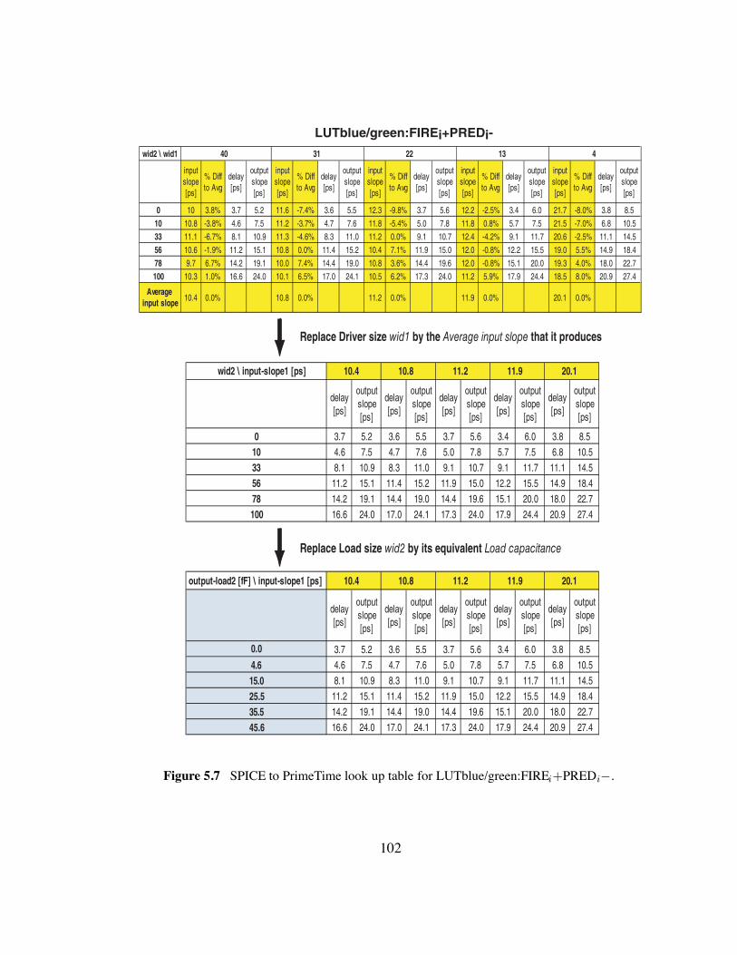
LUTblue/green:FIREi+PREDi-
Replace Driver size wid1 by the Average input slope that it produces
Replace Load size wid2 by its equivalent Load capacitance
wid2 \ input-slope1 [ps] 10.4 10.8 11.2 11.9 20.1
delay[ps]
outputslope[ps]
delay[ps]
outputslope[ps]
delay[ps]
outputslope[ps]
delay[ps]
outputslope[ps]
delay[ps]
outputslope[ps]
0 3.7 5.2 3.6 5.5 3.7 5.6 3.4 6.0 3.8 8.510 4.6 7.5 4.7 7.6 5.0 7.8 5.7 7.5 6.8 10.533 8.1 10.9 8.3 11.0 9.1 10.7 9.1 11.7 11.1 14.556 11.2 15.1 11.4 15.2 11.9 15.0 12.2 15.5 14.9 18.478 14.2 19.1 14.4 19.0 14.4 19.6 15.1 20.0 18.0 22.7100 16.6 24.0 17.0 24.1 17.3 24.0 17.9 24.4 20.9 27.4
output-load2 [fF] \ input-slope1 [ps] 10.4 10.8 11.2 11.9 20.1
delay[ps]
outputslope[ps]
delay[ps]
outputslope[ps]
delay[ps]
outputslope[ps]
delay[ps]
outputslope[ps]
delay[ps]
outputslope[ps]
0.0 3.7 5.2 3.6 5.5 3.7 5.6 3.4 6.0 3.8 8.54.6 4.6 7.5 4.7 7.6 5.0 7.8 5.7 7.5 6.8 10.515.0 8.1 10.9 8.3 11.0 9.1 10.7 9.1 11.7 11.1 14.525.5 11.2 15.1 11.4 15.2 11.9 15.0 12.2 15.5 14.9 18.435.5 14.2 19.1 14.4 19.0 14.4 19.6 15.1 20.0 18.0 22.745.6 16.6 24.0 17.0 24.1 17.3 24.0 17.9 24.4 20.9 27.4
wid2 \ wid1 40 31 22 13 4
inputslope[ps]
% Diffto Avg
delay[ps]
outputslope[ps]
inputslope[ps]
% Diffto Avg
delay[ps]
outputslope[ps]
inputslope[ps]
% Diffto Avg
delay[ps]
outputslope[ps]
inputslope[ps]
% Diffto Avg
delay[ps]
outputslope[ps]
inputslope[ps]
% Diffto Avg
delay[ps]
outputslope[ps]
0 10 3.8% 3.7 5.2 11.6 -7.4% 3.6 5.5 12.3 -9.8% 3.7 5.6 12.2 -2.5% 3.4 6.0 21.7 -8.0% 3.8 8.510 10.8 -3.8% 4.6 7.5 11.2 -3.7% 4.7 7.6 11.8 -5.4% 5.0 7.8 11.8 0.8% 5.7 7.5 21.5 -7.0% 6.8 10.533 11.1 -6.7% 8.1 10.9 11.3 -4.6% 8.3 11.0 11.2 0.0% 9.1 10.7 12.4 -4.2% 9.1 11.7 20.6 -2.5% 11.1 14.556 10.6 -1.9% 11.2 15.1 10.8 0.0% 11.4 15.2 10.4 7.1% 11.9 15.0 12.0 -0.8% 12.2 15.5 19.0 5.5% 14.9 18.478 9.7 6.7% 14.2 19.1 10.0 7.4% 14.4 19.0 10.8 3.6% 14.4 19.6 12.0 -0.8% 15.1 20.0 19.3 4.0% 18.0 22.7100 10.3 1.0% 16.6 24.0 10.1 6.5% 17.0 24.1 10.5 6.2% 17.3 24.0 11.2 5.9% 17.9 24.4 18.5 8.0% 20.9 27.4
Averageinput slope 10.4 0.0% 10.8 0.0% 11.2 0.0% 11.9 0.0% 20.1 0.0%
Figure 5.7 SPICE to PrimeTime look up table for LUTblue/green:FIREi+PREDi".
102
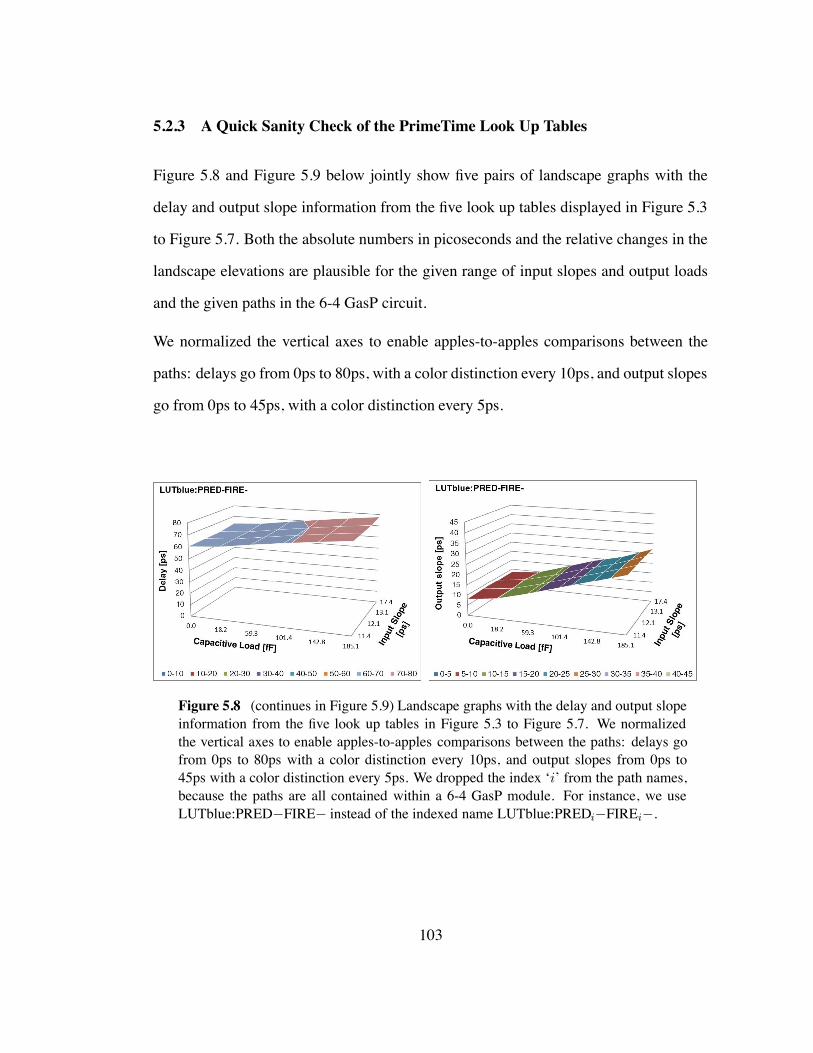
5.2.3 A Quick Sanity Check of the PrimeTime Look Up Tables
Figure 5.8 and Figure 5.9 below jointly show five pairs of landscape graphs with the
delay and output slope information from the five look up tables displayed in Figure 5.3
to Figure 5.7. Both the absolute numbers in picoseconds and the relative changes in the
landscape elevations are plausible for the given range of input slopes and output loads
and the given paths in the 6-4 GasP circuit.
We normalized the vertical axes to enable apples-to-apples comparisons between the
paths: delays go from 0ps to 80ps, with a color distinction every 10ps, and output slopes
go from 0ps to 45ps, with a color distinction every 5ps.
Figure 5.8 (continues in Figure 5.9) Landscape graphs with the delay and output slopeinformation from the five look up tables in Figure 5.3 to Figure 5.7. We normalizedthe vertical axes to enable apples-to-apples comparisons between the paths: delays gofrom 0ps to 80ps with a color distinction every 10ps, and output slopes from 0ps to45ps with a color distinction every 5ps. We dropped the index ‘i’ from the path names,because the paths are all contained within a 6-4 GasP module. For instance, we useLUTblue:PRED"FIRE" instead of the indexed name LUTblue:PREDi"FIREi".
103
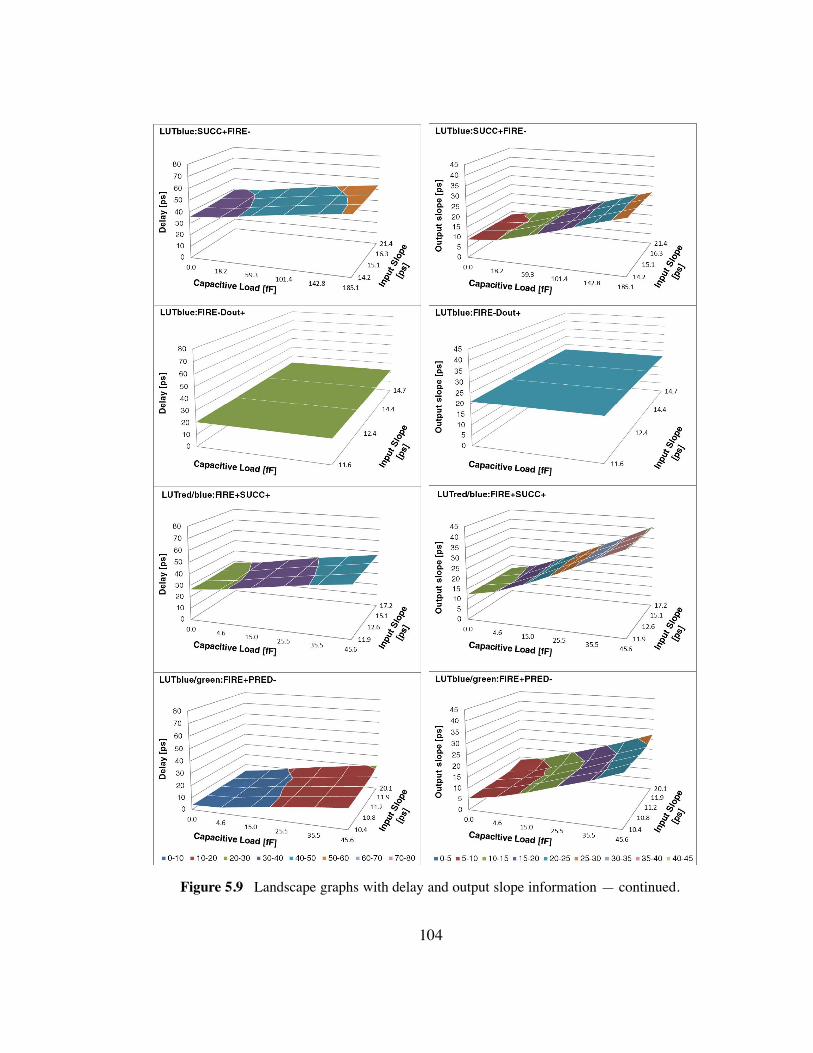
Figure 5.9 Landscape graphs with delay and output slope information — continued.
104
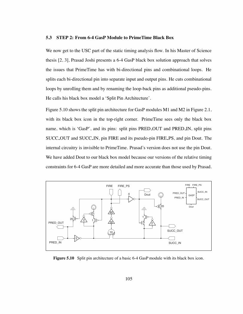
5.3 STEP 2: From 6-4 GasP Module to PrimeTime Black Box
We now get to the USC part of the static timing analysis flow. In his Master of Science
thesis [2, 3], Prasad Joshi presents a 6-4 GasP black box solution approach that solves
the issues that PrimeTime has with bi-directional pins and combinational loops. He
splits each bi-directional pin into separate input and output pins. He cuts combinational
loops by unrolling them and by renaming the loop-back pins as additional pseudo-pins.
He calls his black box model a ‘Split Pin Architecture’.
Figure 5.10 shows the split pin architecture for GasP modules M1 and M2 in Figure 2.1,
with its black box icon in the top-right corner. PrimeTime sees only the black box
name, which is ‘GasP’, and its pins: split pins PRED OUT and PRED IN, split pins
SUCC OUT and SUCC IN, pin FIRE and its pseudo-pin FIRE PS, and pin Dout. The
internal circuitry is invisible to PrimeTime. Prasad’s version does not use the pin Dout.
We have added Dout to our black box model because our versions of the relative timing
constraints for 6-4 GasP are more detailed and more accurate than those used by Prasad.
GASP
FIRE FIRE_PS
PRED_IN
PRED_OUT SUCC_IN
SUCC_OUT
201
1
1
1
20
PRED_IN SUCC_IN
FIRE
PRED_OUT
SUCC_OUT
30
80
5
2
4
2
10
Dout
Dout
FIRE_PS
Figure 5.10 Split pin architecture of a basic 6-4 GasP module with its black box icon.
105
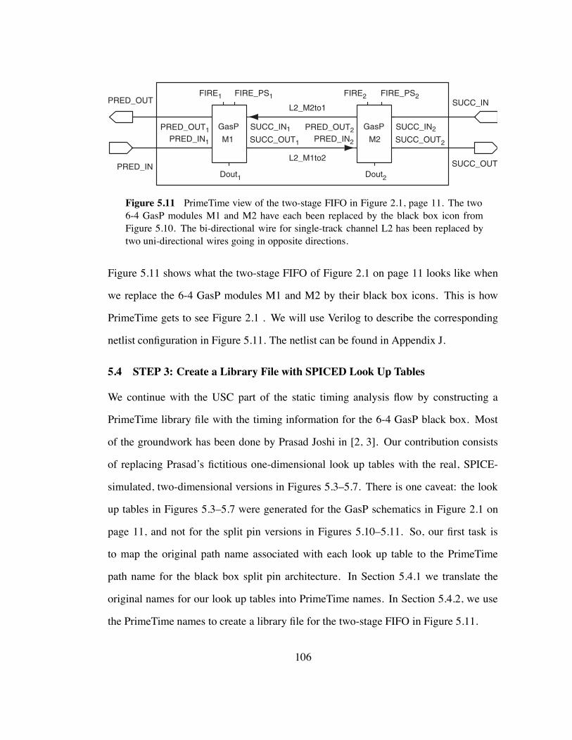
M2
FIRE_PS2FIRE2FIRE1 FIRE_PS1
M1
PRED_IN
PRED_OUT
PRED_IN1
PRED_OUT1PRED_IN2
PRED_OUT2
SUCC_OUT
SUCC_IN
SUCC_OUT2
SUCC_IN2
SUCC_OUT1
SUCC_IN1 GasPGasP
Dout2Dout1
L2_M1to2
L2_M2to1
Figure 5.11 PrimeTime view of the two-stage FIFO in Figure 2.1, page 11. The two6-4 GasP modules M1 and M2 have each been replaced by the black box icon fromFigure 5.10. The bi-directional wire for single-track channel L2 has been replaced bytwo uni-directional wires going in opposite directions.
Figure 5.11 shows what the two-stage FIFO of Figure 2.1 on page 11 looks like when
we replace the 6-4 GasP modules M1 and M2 by their black box icons. This is how
PrimeTime gets to see Figure 2.1 . We will use Verilog to describe the corresponding
netlist configuration in Figure 5.11. The netlist can be found in Appendix J.
5.4 STEP 3: Create a Library File with SPICED Look Up Tables
We continue with the USC part of the static timing analysis flow by constructing a
PrimeTime library file with the timing information for the 6-4 GasP black box. Most
of the groundwork has been done by Prasad Joshi in [2, 3]. Our contribution consists
of replacing Prasad’s fictitious one-dimensional look up tables with the real, SPICE-
simulated, two-dimensional versions in Figures 5.3–5.7. There is one caveat: the look
up tables in Figures 5.3–5.7 were generated for the GasP schematics in Figure 2.1 on
page 11, and not for the split pin versions in Figures 5.10–5.11. So, our first task is
to map the original path name associated with each look up table to the PrimeTime
path name for the black box split pin architecture. In Section 5.4.1 we translate the
original names for our look up tables into PrimeTime names. In Section 5.4.2, we use
the PrimeTime names to create a library file for the two-stage FIFO in Figure 5.11.
106
5.4.1 STEP 3.1: Rename Look Up Tables to Match Black Box Names
This section discusses our approach in renaming the input and output signal names and
relative timing paths in the original two-stage GasP FIFO in Figure 2.1, page 11, to the
corresponding names and paths in the new two-stage black box FIFO in Figure 5.11,
with the black box as defined in Figure 5.10. Our renaming follows the renaming that
Prasad took in his Master of Science thesis [2]. Nevertheless, we would like to explicitly
emphasize the renaming part, because it is less trivial than one might think. The crux
in making a valid renaming for signal names is to make it valid for what we do with
PrimeTime and for what PrimeTime does with these names.
We use PrimeTime to validate the relative timing constraints RT1 to RT4 of Figure 2.2,
page 13. This means that we instruct PrimeTime to compare the timing results of the red
and the blue paths in RT1 in Figure 2.2(a), and to validate that the delay of the red path
is less than that of the blue path. It also means that we instruct PrimeTime to compare
the timing results of the green and the blue paths in RT3 in Figure 2.2(c), and to validate
that the delay of the green path is less than that of the blue path. We instruct PrimeTime
to do similar comparisons for RT2 and RT4 – see Figure 2.2 for details. PrimeTime
may use only the input and output signals names that the black box icon allows it to
see. It uses these names to construct a path through the circuit, to time this path, and to
compare the timing information of this particular path to that of other paths. PrimeTime
can connect black box signal names in precisely two ways. It connects the signal names
if either the netlist or a look up table connects them.
For a valid renaming, the connectivity that PimeTime sees must match the connectivity
in Figure 2.2. One way to achieve this is to redraw Figure 2.2 with black box signal
names, and to make sure that the connectivity matches that of the original Figure 2.2.
107
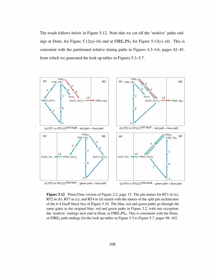
The result follows below in Figure 5.12. Note that we cut off the ‘nodrive’ paths end-
ings at Dout1 for Figure 5.12(a)–(b) and at FIRE PS2 for Figure 5.12(c)–(d). This is
consistent with the partitioned relative timing paths in Figures 4.3–4.6, pages 42–45,
from which we generated the look up tables in Figures 5.3–5.7.
PRED_OUT2-
FIRE2+FIRE_PS2-
A
B
C
X
SUCC_IN1-
F
(d) RT4 or RT(L2)TrfB-RstB : green path < blue path
L2
D
FIRE1+FIRE_PS1-
A
B
C Dout1
E
DM1 M2
(b) RT2 or RT(L2)TrfF-RstF : red path < blue path
A
B
C
FIRE2+FIRE_PS2-
PRED_OUT2- SUCC_OUT2+
XE
D
SUCC_IN1-
(c) RT3 or RT(L2)TrfB-RstF : green path < blue path
L2
FIRE1+FIRE_PS1-
PRED_OUT1- SUCC_OUT1+
A
B
C
X
F
E
D
D
Dout1PRED_IN2+
M1 M2
M1 M2M1 M2
(a) RT1 or RT(L2)TrfF-RstB : red path < blue path
L2SUCC_OUT1+ PRED_IN2+
L2
Figure 5.12 PrimeTime version of Figure 2.2, page 13. The pin names for RT1 in (a),RT2 in (b), RT3 in (c), and RT4 in (d) match with the names of the split pin architectureof the 6-4 GasP black box of Figure 5.10. The blue, red and green paths go through thesame gates as the original blue, red and green paths in Figure 2.2, with one exception:the ‘nodrive’ endings now end in Dout1 or FIRE PS2. This is consistent with the Dout1or FIRE2 path endings for the look up tables in Figure 5.3 to Figure 5.7, pages 98–102.
108
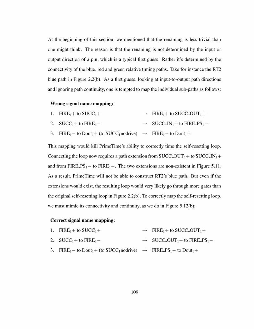
At the beginning of this section, we mentioned that the renaming is less trivial than
one might think. The reason is that the renaming is not determined by the input or
output direction of a pin, which is a typical first guess. Rather it’s determined by the
connectivity of the blue, red and green relative timing paths. Take for instance the RT2
blue path in Figure 2.2(b). As a first guess, looking at input-to-output path directions
and ignoring path continuity, one is tempted to map the individual sub-paths as follows:
Wrong signal name mapping:
1. FIRE1+ to SUCC1+ $ FIRE1+ to SUCC OUT1+
2. SUCC1+ to FIRE1" $ SUCC IN1+ to FIRE PS1"
3. FIRE1" to Dout1+ (to SUCC1nodrive) $ FIRE1" to Dout1+
This mapping would kill PrimeTime’s ability to correctly time the self-resetting loop.
Connecting the loop now requires a path extension from SUCC OUT1+ to SUCC IN1+
and from FIRE PS1" to FIRE1". The two extensions are non-existent in Figure 5.11.
As a result, PrimeTime will not be able to construct RT2’s blue path. But even if the
extensions would exist, the resulting loop would very likely go through more gates than
the original self-resetting loop in Figure 2.2(b). To correctly map the self-resetting loop,
we must mimic its connectivity and continuity, as we do in Figure 5.12(b):
Correct signal name mapping:
1. FIRE1+ to SUCC1+ $ FIRE1+ to SUCC OUT1+
2. SUCC1+ to FIRE1" $ SUCC OUT1+ to FIRE PS1"
3. FIRE1" to Dout1+ (to SUCC1nodrive) $ FIRE PS1" to Dout1+
109
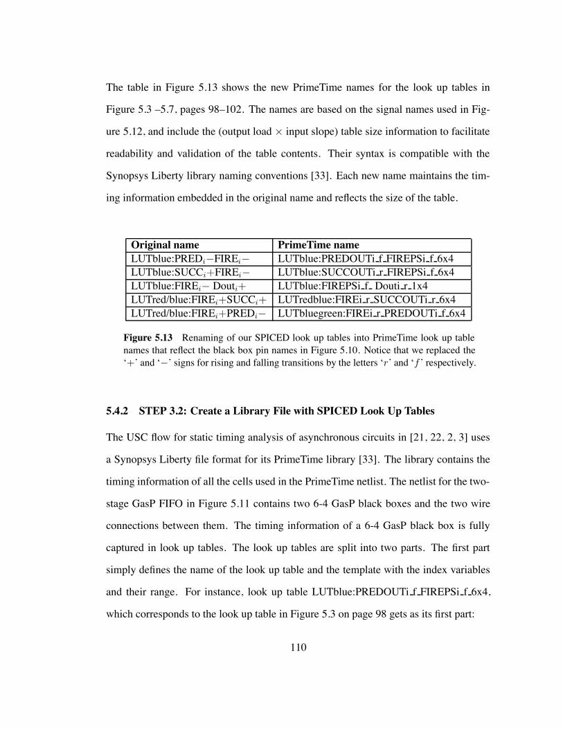
The table in Figure 5.13 shows the new PrimeTime names for the look up tables in
Figure 5.3 –5.7, pages 98–102. The names are based on the signal names used in Fig-
ure 5.12, and include the (output load # input slope) table size information to facilitate
readability and validation of the table contents. Their syntax is compatible with the
Synopsys Liberty library naming conventions [33]. Each new name maintains the tim-
ing information embedded in the original name and reflects the size of the table.
Original name PrimeTime nameLUTblue:PREDi"FIREi" LUTblue:PREDOUTi f FIREPSi f 6x4LUTblue:SUCCi+FIREi" LUTblue:SUCCOUTi r FIREPSi f 6x4LUTblue:FIREi" Douti+ LUTblue:FIREPSi f Douti r 1x4LUTred/blue:FIREi+SUCCi+ LUTredblue:FIREi r SUCCOUTi r 6x4LUTred/blue:FIREi+PREDi" LUTbluegreen:FIREi r PREDOUTi f 6x4
Figure 5.13 Renaming of our SPICED look up tables into PrimeTime look up tablenames that reflect the black box pin names in Figure 5.10. Notice that we replaced the‘+’ and ‘"’ signs for rising and falling transitions by the letters ‘r’ and ‘f ’ respectively.
5.4.2 STEP 3.2: Create a Library File with SPICED Look Up Tables
The USC flow for static timing analysis of asynchronous circuits in [21, 22, 2, 3] uses
a Synopsys Liberty file format for its PrimeTime library [33]. The library contains the
timing information of all the cells used in the PrimeTime netlist. The netlist for the two-
stage GasP FIFO in Figure 5.11 contains two 6-4 GasP black boxes and the two wire
connections between them. The timing information of a 6-4 GasP black box is fully
captured in look up tables. The look up tables are split into two parts. The first part
simply defines the name of the look up table and the template with the index variables
and their range. For instance, look up table LUTblue:PREDOUTi f FIREPSi f 6x4,
which corresponds to the look up table in Figure 5.3 on page 98 gets as its first part:
110
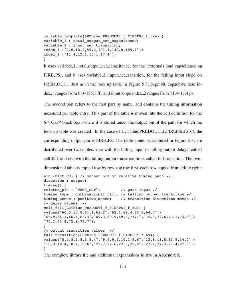
lu_table_template(LUTblue_PREDOUTi_f_FIREPSi_f_6x4) {variable_1 : total_output_net_capacitance;variable_2 : input_net_transition;index_1 ("0.0,18.2,59.3,101.4,142.8,185.1");index_2 ("11.4,12.1,13.1,17.4");}
It uses variable 1, total output net capacitance, for the (external) load capacitance on
FIRE PSi, and it uses variable 2, input net transition, for the falling input slope on
PRED OUTi. Just as in the look up table in Figure 5.3, page 98, capacitive load in-
dex 1 ranges from 0.0–185.1 fF, and input slope index 2 ranges from 11.4–17.4 ps.
The second part refers to the first part by name, and contains the timing information
measured per table entry. This part of the table is moved into the cell definition for the
6-4 GasP black box, where it is stored under the output pin of the path for which the
look up table was created. In the case of LUTblue:PREDOUTi f FIREPSi f 6x4, the
corresponding output pin is FIRE PS. The table contents, captured in Figure 5.3, are
distributed over two tables: one with the falling input to falling output delays, called
cell fall, and one with the falling output transition time, called fall transition. The two-
dimensional table is copied row by row, top row first, each row copied from left to right:
pin (FIRE_PS) { /* output pin of relative timing path */direction : output;timing() {related_pin : "PRED_OUT"; /* path input */timing_type : combinational_fall; /* falling output transition */timing_sense : positive_unate; /* transition directions match *//* delay values */cell_fall(LUTblue_PREDOUTi_f_FIREPSi_f_6x4) {values("60.3,60.8,61.1,63.2","62.1,62.4,62.8,64.7",\"65.9,66.1,66.6,68.3","69.3,69.5,69.9,71.7","72.3,72.6,73.1,74.8",\"75.1,75.4,75.9,77.7");}/* output transition values */fall_transition(LUTblue_PREDOUTi_f_FIREPSi_f_6x4) {values("8.0,8.5,8.3,8.4","9.9,9.9,10.1,9.6","13.8,13.8,13.9,14.0",\"18.3,18.4,18.4,18.6","22.7,22.6,22.3,22.0","27.1,27.3,27.4,27.3");}
The complete library file and additional explanations follow in Appendix K.
111
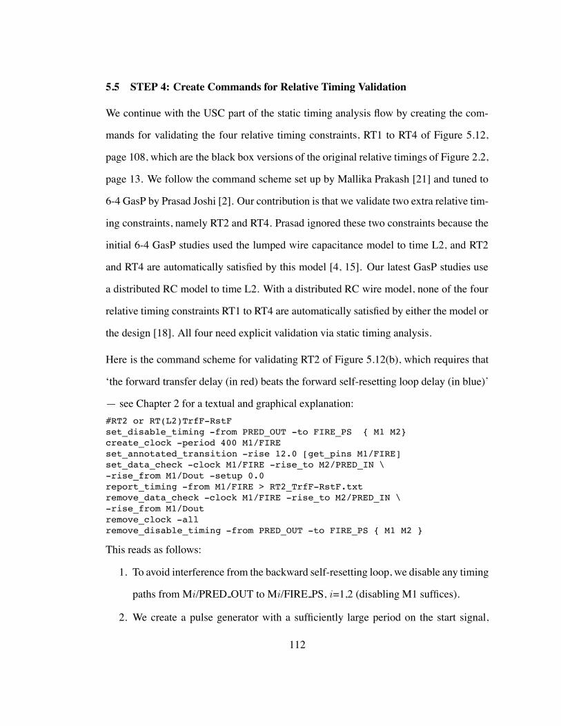
5.5 STEP 4: Create Commands for Relative Timing Validation
We continue with the USC part of the static timing analysis flow by creating the com-
mands for validating the four relative timing constraints, RT1 to RT4 of Figure 5.12,
page 108, which are the black box versions of the original relative timings of Figure 2.2,
page 13. We follow the command scheme set up by Mallika Prakash [21] and tuned to
6-4 GasP by Prasad Joshi [2]. Our contribution is that we validate two extra relative tim-
ing constraints, namely RT2 and RT4. Prasad ignored these two constraints because the
initial 6-4 GasP studies used the lumped wire capacitance model to time L2, and RT2
and RT4 are automatically satisfied by this model [4, 15]. Our latest GasP studies use
a distributed RC model to time L2. With a distributed RC wire model, none of the four
relative timing constraints RT1 to RT4 are automatically satisfied by either the model or
the design [18]. All four need explicit validation via static timing analysis.
Here is the command scheme for validating RT2 of Figure 5.12(b), which requires that
‘the forward transfer delay (in red) beats the forward self-resetting loop delay (in blue)’
— see Chapter 2 for a textual and graphical explanation:#RT2 or RT(L2)TrfF-RstFset_disable_timing -from PRED_OUT -to FIRE_PS { M1 M2}create_clock -period 400 M1/FIREset_annotated_transition -rise 12.0 [get_pins M1/FIRE]set_data_check -clock M1/FIRE -rise_to M2/PRED_IN \-rise_from M1/Dout -setup 0.0report_timing -from M1/FIRE > RT2_TrfF-RstF.txtremove_data_check -clock M1/FIRE -rise_to M2/PRED_IN \-rise_from M1/Doutremove_clock -allremove_disable_timing -from PRED_OUT -to FIRE_PS { M1 M2 }
This reads as follows:
1. To avoid interference from the backward self-resetting loop, we disable any timing
paths from Mi/PRED OUT to Mi/FIRE PS, i=1,2 (disabling M1 suffices).
2. We create a pulse generator with a sufficiently large period on the start signal,
112
a.k.a. ‘Point of Divergence’, for the blue and the red paths in RT2, i.e. on
M1/FIRE. We are interested in the rising transition on M1/FIRE, which we de-
fine to be a nominal 20%-80% rise time of 12ps.
3. We request PrimeTime to validate that the delay of the forward transfer from
M1/FIRE to M2/PRED (the red path), is smaller than the delay of the forward
self-resetting loop from M1/FIRE to M1/Dout (the blue path) with a minimum
slack of 0.0ps, and to report the timing results to output file ‘RT2 TrfF-RstF.txt’.
4. We clean up any side effects, so the next command scheme starts from scratch.
The full command file can be found in Appendix L.
5.6 STEP 5: Run and Inspect Timing Reports
The PrimeTime run commands follow in the introduction of Appendix M. The output
files with the timing reports for the four relative timing constraints RT1 to RT4 follow in
Appendices M.1–M.4. We verified that the delay times generated by PrimeTime can be
generated using linear interpolation and linear extrapolation on the look up table entries
in Figure 5.3–5.7, pages 98–102, using the look up table re-naming in Figure 5.13 on
page 110. As an example, we will show how we verified the PrimeTime delays for RT2:
1. RT2 red and blue path, from M1/FIRE+ to M1/SUCC OUT+
• M1/FIRE receives a rising transition with a rise time of 12ps, measured from
when the signal voltage passes 20% VDD to when it reaches 80% VDD. Our
simulation setup uses a default external output load of 0fF for this path.
• A table entry with an input slope of 12ps and output load of 0fF falls within
the look up table range for LUTredblue:FIREi r SUCCOUTi r 6x4, which
translates to the look up table name LUTred/blue:FIREi+SUCCi+ with ta-
ble entries in Figure 5.6 (bottom), page 101.
113
• In Figure 5.6 (bottom), the non-existent entry (0.0fF,12ps) falls between the
existing entry (0.0fF,11.9ps), which has a delay of 26.3ps and an output slope
of 12.2ps, and the existing entry (0.0fF,12.6ps), which has a delay of 26.7ps
and an output slope of 12.5ps. Linear interpolation thus gives:
delay(0.0fF,12ps) = 26.3ps + ((12-11.9)/(12.6-11.9))#0.4ps = 26.36ps
output slope(0.0fF,12ps) = 12.2 + ((12-11.9)/(12.6-11.9))#0.3 = 12.24ps
• The delay number matches exactly with the delay given by PrimeTime.
2. RT2 red path, from M1/SUCC OUT+ to M2/PRED IN+ via L2
• This path has no timing information. PrimeTime correctly gives 0.0ps delay.
3. RT2 blue path, from M1/SUCC OUT+ to M1/FIRE PS-
• The predecessor blue path in item 1 ended with an output slope of 12.24ps,
which becomes the input slope for this path. Our simulation setup uses a
default external output load of 0fF for this path.
• A table entry with an input slope of 12.24ps and output load of 0fF falls out-
side the look up table range for LUTblue:SUCCOUTi r FIREi f 6x4, which
translates to the look up table name LUTblue:SUCCi+FIREi" with table
entries in Figure 5.4 (bottom), page 99.
• In Figure 5.4 (bottom), non-existent entry (0.0fF,12.24ps) falls beyond the
existing entry (0.0fF,14.2ps), which has a delay of 35.8ps and an output slope
of 8.8ps, and beyond the existing entry (0.0fF,15.1ps),which has a delay of
36.3ps and an output slope of 8.6ps. Linear extrapolation thus gives:
delay(0.0fF,12.24ps)= 35.8ps - ((14.2-12.24)/(15.1-14.2))#0.5ps = 34.71ps
output slope(0.0fF,12.24ps)= 8.8 + ((14.2-12.24)/(15.1-14.2))#0.2= 9.24ps
• The delay number matches exactly with the delay given by PrimeTime.
114
4. RT2 blue path, from M1/FIRE PS- to M1/Dout+
• The predecessor blue path in item 3 ended with an output slope of 9.24ps,
which becomes the input slope for this path. Our simulation setup uses a
default external output load of 0fF for this path.
• A table entry with an input slope of 9.24ps and an output load of 0fF falls
outside the look up table range for LUTblue:FIREPSi f Douti r 1x4. This
table name translates to the look up table name LUTblue:FIREi"Douti+
with table entries in Figure 5.5 (bottom), page 100.
• In Figure 5.5 (bottom), the non-existent entry (0.0fF, 9.24ps) falls beyond the
existing entries (0.0fF, 11.6ps) and (0.0fF, 12.4ps), which have delays 20.5ps
respectively 20.9ps. The output slope is irrelevant in this case, because the
RT blue path ends here. Linear extrapolation thus gives:
delay(0.0fF, 9.24ps) = 20.5ps - ((11.6-9.24)/(12.4-11.6))*0.4ps = 19.32ps
• The delay number matches exactly with the delay given by PrimeTime.
5. RT2 Slack calculation
• The total delay of the red path in RT2 is the sum of items 1–2 = 26.36ps.• The total delay of the blue path is the sum of items 1, 3, and 4 = 80.39ps.
• The slack or (total blue path delay " total red path delay) is thus 54.03ps.
• This is exactly what PrimeTime reports as slack for RT2.
In summary: PrimeTime’s delay calculation for RT2 is based on linear interpolation and
linear extrapolation of the table entries in our look up tables. This is also true for the
PrimeTime delay calculations of the three other relative timing constraints, RT1, RT3,
and RT4.
115
RT2 has a reported slack of 54.03ps. The reason why this slack is so large is because
the L2 wire delay for the red path takes 0ps in the current simulation setup, as can
be seen in item 2 in the above validation reasoning for RT2. This implies that the
delay for a rising transition from the near end of L2 (M1/SUCC OUT) to the far end of
L2 (M2/PRED IN) can take up to 54.03ps. A delay beyond 54.03ps invalidates RT2.
Invalidating RT2 amounts to M1 stopping its drive before M2 sees the transition. This
does not immediately invalidate the circuit operation, as we demonstrate in [18], but it
makes the circuit less robust and more noise sensitive. In Chapter 6 we will compare the
PrimeTime results to the results of our short-to-medium-to-long wire study in [18].
5.7 Conclusion and Future Work for Chapter 5
Chapter 5 is the “proof of the pudding” as we call it in the the conclusion sections of
Chapters 3 and 4. It concludes our quest to create a flow for library characterization and
static timing analysis of single-track circuits in GasP.
In Chapter 3, we showed how SPICE can be used to generate the timing information
of a simple circuit without loops and without single-track communication wires, and
to capture that information in look up tables. Our quest in Chapter 3 was more of a
warming-up quest to understand enough of the design environment in Electric and of
the simulation environment in SPICE to make things work.
The real quest came in Chapter 4, where we showed how to partition the circuit and
the timing constraints that it needs to make the SPICE approach of Chapter 3 work for
full-fledged GasP circuits with loops and single-track communication wires. Our timing
characterization flow in Chapter 4 is new, as far as we know.
116

In Chapter 5, we took the look up tables that we generated in Chapter 4, and fed them
to a standard static timing analysis (STA) flow, namely PrimeTime of Synopsys. The
STA flow is not new: it was specifically created for asynchronous or self-timed circuits
at the University of Southern California (USC), by Mallika Prakash and Prasad Joshi —
two former Master of Science students in the research group of Professor Peter Beerel.
Having access to the USC STA flow for asynchronous circuits was a major help in
completing our quest. It limited the final stretch of our quest to (1) importing our look
up tables into PrimeTime and (2) validating the timing reports and comparing them to
the results of our earlier studies published in [18]. Chapter 5 is primarily about (1) and
(2), but it also fills in and explains the connections to the USC flow.
Last but not least: not only did we (1) generate and (2) explain a timing validation flow
for single-track circuits in 6-4 GasP but we also (3) used this flow and we (4) validated
its results. The many files in Appendices A–M in this thesis bear witness to this. For
truly: the proof of the pudding is in the eating.
As far as future work goes, we covered most of it in the conclusions of Chapters 3–4.
Key to static timing analysis are: flow automation and wire delay models.
117
Chapter 6
SUMMARY AND DISCUSSION OF TIMING RESULTS
The slack timings computed by PrimeTime and reported in Appendices M.1–M.4 are
between 50.29ps and 57.66ps. RT2, for instance, has a reported slack of 54.03ps. The
reason why this slack is so large is because the L2 wire delay for the red path takes
0ps in the current simulation setup — as we can see in item 2 for the R2 validation
reasoning of the PrimeTime results in Section 5.6. The implication of this is that the
delay for a rising transition from the near end of L2 (M1/SUCC OUT) to the far end of
L2 (M2/PRED IN) can take up to 54.03ps. A delay beyond 54.03ps invalidates RT2.
Invalidating RT2 amounts to M1 stopping its drive before M2 sees the transition. This
does not immediately invalidate the circuit operation, as we demonstrate in [18], but it
makes the circuit less robust and more noise sensitive.
The 54.03ps slack that PrimeTime reports for RT2 is 20–25% smaller than the slack
that we reported in [18]. The reason for this 20-25% difference is that our PrimeTime
simulations use 0fF external output loads, whereas the simulations in [18] use realistic
output loads. The difference in slack between the red and blue paths (ignoring L2) comes
from four gates in the blue path: gates A, B, C, and D in Module M1 of Figure 2.1,
page 11. The outputs of gates A, B and D are internal to the circuit, but the output of
118
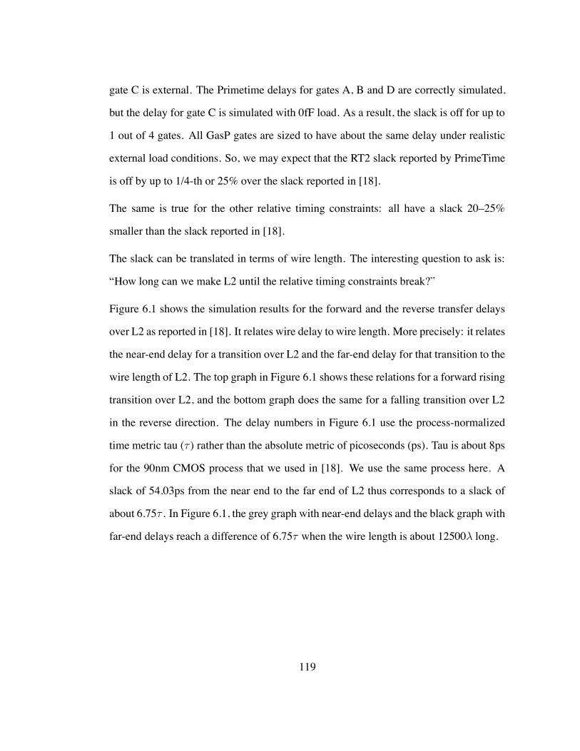
gate C is external. The Primetime delays for gates A, B and D are correctly simulated,
but the delay for gate C is simulated with 0fF load. As a result, the slack is off for up to
1 out of 4 gates. All GasP gates are sized to have about the same delay under realistic
external load conditions. So, we may expect that the RT2 slack reported by PrimeTime
is off by up to 1/4-th or 25% over the slack reported in [18].
The same is true for the other relative timing constraints: all have a slack 20–25%
smaller than the slack reported in [18].
The slack can be translated in terms of wire length. The interesting question to ask is:
“How long can we make L2 until the relative timing constraints break?”
Figure 6.1 shows the simulation results for the forward and the reverse transfer delays
over L2 as reported in [18]. It relates wire delay to wire length. More precisely: it relates
the near-end delay for a transition over L2 and the far-end delay for that transition to the
wire length of L2. The top graph in Figure 6.1 shows these relations for a forward rising
transition over L2, and the bottom graph does the same for a falling transition over L2
in the reverse direction. The delay numbers in Figure 6.1 use the process-normalized
time metric tau (! ) rather than the absolute metric of picoseconds (ps). Tau is about 8ps
for the 90nm CMOS process that we used in [18]. We use the same process here. A
slack of 54.03ps from the near end to the far end of L2 thus corresponds to a slack of
about 6.75! . In Figure 6.1, the grey graph with near-end delays and the black graph with
far-end delays reach a difference of 6.75! when the wire length is about 12500" long.
119
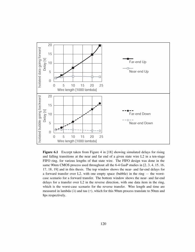
Del
ay [!
]D
elay
[!]
Wire length [1000 lambda]
Wire length [1000 lambda]
Far-end Down
Far-end Up
Near-end Down
Near-end Up
0
5
10
15
20
0 5 10 15 20 25
0
5
10
15
20
0 5 10 15 20 25
Isol
ated
dat
a go
ing
forw
ard
Isol
ated
bub
ble
goin
g ba
ckw
ard
Figure 6.1 Excerpt taken from Figure 4 in [18] showing simulated delays for risingand falling transitions at the near and far end of a given state wire L2 in a ten-stageFIFO ring, for various lengths of that state wire. The FIFO design was done in thesame 90nm CMOS process used throughout all the 6-4 GasP studies in [2, 3, 4, 15, 16,17, 18, 19] and in this thesis. The top window shows the near- and far-end delays fora forward transfer over L2, with one empty space (bubble) in the ring — the worst-case scenario for a forward transfer. The bottom window shows the near- and far-enddelays for a transfer over L2 in the reverse direction, with one data item in the ring,which is the worst-case scenario for the reverse transfer. Wire length and time aremeasured in lambda (!) and tau (" ), which for this 90nm process translate to 50nm and8ps respectively.
120
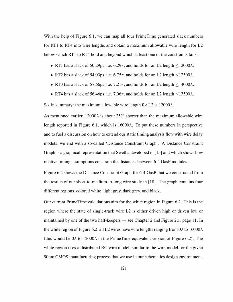
With the help of Figure 6.1, we can map all four PrimeTime generated slack numbers
for RT1 to RT4 into wire lengths and obtain a maximum allowable wire length for L2
below which RT1 to RT4 hold and beyond which at least one of the constraints fails:
• RT1 has a slack of 50.29ps, i.e. 6.29! , and holds for an L2 length &12000".
• RT2 has a slack of 54.03ps, i.e. 6.75! , and holds for an L2 length &12500".
• RT3 has a slack of 57.66ps, i.e. 7.21! , and holds for an L2 length &14000".
• RT4 has a slack of 56.46ps, i.e. 7.06! , and holds for an L2 length &13500".
So, in summary: the maximum allowable wire length for L2 is 12000".
As mentioned earlier, 12000" is about 25% shorter than the maximum allowable wire
length reported in Figure 6.1, which is 16000". To put these numbers in perspective
and to fuel a discussion on how to extend our static timing analysis flow with wire delay
models, we end with a so-called ‘Distance Constraint Graph’. A Distance Constraint
Graph is a graphical representation that Swetha developed in [15] and which shows how
relative timing assumptions constrain the distances between 6-4 GasP modules.
Figure 6.2 shows the Distance Constraint Graph for 6-4 GasP that we constructed from
the results of our short-to-medium-to-long wire study in [18]. The graph contains four
different regions, colored white, light grey, dark grey, and black.
Our current PrimeTime calculations aim for the white region in Figure 6.2. This is the
region where the state of single-track wire L2 is either driven high or driven low or
maintained by one of the two half-keepers — see Chapter 2 and Figure 2.1, page 11. In
the white region of Figure 6.2, all L2 wires have wire lengths ranging from 0" to 16000"
(this would be 0" to 12000" in the PrimeTime-equivalent version of Figure 6.2). The
white region uses a distributed RC wire model, similar to the wire model for the given
90nm CMOS manufacturing process that we use in our schematics design environment.
121
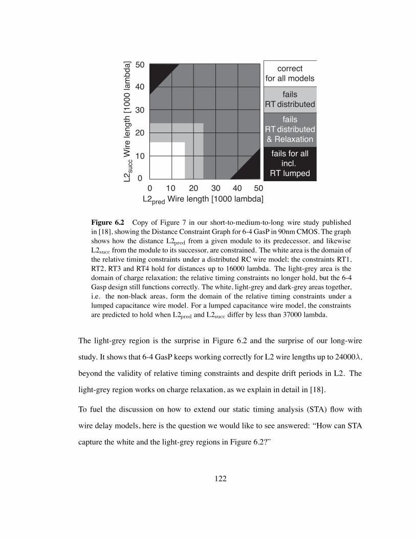
L2pred Wire length [1000 lambda]
L2succ
Wire
length
[1000 lambda]
0 10 20 30 40 500
10
20
30
40
50 correctfor all models
failsRT distributed
fails for allincl.
RT lumped
failsRT distributed& Relaxation
Figure 6.2 Copy of Figure 7 in our short-to-medium-to-long wire study publishedin [18], showing the Distance Constraint Graph for 6-4 GasP in 90nm CMOS. The graphshows how the distance L2pred from a given module to its predecessor, and likewiseL2succ from the module to its successor, are constrained. The white area is the domain ofthe relative timing constraints under a distributed RC wire model; the constraints RT1,RT2, RT3 and RT4 hold for distances up to 16000 lambda. The light-grey area is thedomain of charge relaxation; the relative timing constraints no longer hold, but the 6-4Gasp design still functions correctly. The white, light-grey and dark-grey areas together,i.e. the non-black areas, form the domain of the relative timing constraints under alumped capacitance wire model. For a lumped capacitance wire model, the constraintsare predicted to hold when L2pred and L2succ differ by less than 37000 lambda.
The light-grey region is the surprise in Figure 6.2 and the surprise of our long-wire
study. It shows that 6-4 GasP keeps working correctly for L2 wire lengths up to 24000",
beyond the validity of relative timing constraints and despite drift periods in L2. The
light-grey region works on charge relaxation, as we explain in detail in [18].
To fuel the discussion on how to extend our static timing analysis (STA) flow with
wire delay models, here is the question we would like to see answered: “How can STA
capture the white and the light-grey regions in Figure 6.2?”
122

Chapter 7
COMPARISON TO RELATED WORK
Our research builds upon prior research work presented and published by Mallika
Prakash [21, 22] and Prasad Joshi [2, 3] — two former Master of Science students in the
research group of Professor Peter Beerel at the University of Southern California (USC).
Mallika investigated and developed a library characterization and static timing analysis
flow for asynchronous circuits with uni-directional communication channels. Her work
covers power as well as timing characterization. Prasad extended Mallika’s static tim-
ing analysis solution to circuits with bi-directional channels. Specifically, he covered
the bi-directional communication mechanism for single-track handshaking that we use
in 6-4 GasP. Prasad did not extend Mallika’s look up table characterization approach to
6-4 GasP — the look up tables in his work are fictional.
The look up table generation approach that we present in Chapters 3–4 differs from
Mallika’s approach in two major ways:
• Mallika’s thesis partly covers single-track circuits. She presents a simulation envi-
ronment that simulates the asynchronous circuit in its entirety to characterize for-
ward and reverse latencies for various input slopes and output loads. This suffices
to characterize the throughput of the circuit, but is insufficient for characterizing
123
and validating the circuit’s relative timing constraints, i.e. timing assumptions on
which the correct operation of the circuit depends. To generate look up tables
for validating relative timing constraints in GasP, we must open up the circuit
and simulate specific internal paths. The library characterization method that we
created and which we describe in Chapters 3–4 does exactly that.
• The asynchronous circuits investigated by Mallika are all two-ported devices:
there is a data input side and a data output side. GasP is a three-ported device.
Module M1 in Figure 2.1 has a predecessor input, PRED1, a FIRE1 signal to cap-
ture the data, and a successor output, SUCC1. As a result, the approach to look
up table generation for Mallika is a straightforward two-dimensional simulation
process from (input-drive# output-load)$ timing. In contrast, GasP requires:
1. either a table for (input-drive# load-on-FIRE1 # output-load)$ timing,
which is a three-dimensional look up table,
2. or a partitioning into two-dimensional look up tables,
3. or a pre-defined single-rail datapath design with a fixed load on FIRE1, to
turn GasP into a two-ported device with two-dimensional look up tables.
Lacking a fixed load on FIRE1, we present a solution in the style of item 2 above,
because this requires fewer simulations than a solution approach based on item 1.
An additional difference between the USC flow and our version that is worth mentioning
is the way that wires are modeled. In the USC flow, the wires are included with a
lumped capacitance model. In contrast, we separate the wire models from our look up
table generation process, and make them a plug-and-play object that we can insert later
when we run static timing analysis. Our motivation to do so comes from the short-to-
medium-to-long wire studies that we did for 6-4 GasP and which we published in [18].
124

The results of these wire studies show that there are two crucial ingredients that make a
good sender-receiver wire model:
1. The capacitive load at the near end of the wire, as seen by the sender, as a function
of the wire length, width, spacing, and the load capacitance at the wire’s far-end:
• For GasP, this information will be used to simulate the relative timing paths
related to the blue-colored self-resetting loops in Figures 2.1, 2.2, and 5.12
on pages 11, 13 and 108 respectively.
2. Wire resistance and capacitive wire load as seen by the receiver — again as a
function of wire length, width, spacing, and the capacitive load at the far-end:
• For GasP, this information will be used to simulate the relative timing paths
related to the forward red-colored arrows and reverse green-colored arrows
in Figures 2.1 and 2.2 and 5.12 on pages 11, 13 and 108 respectively.
125
Chapter 8
CONCLUSION AND FUTUREWORK
In this thesis, I have created a timing validation flow for single-track circuits in 6-4 GasP.
The flow consists of two parts: library characterization and static timing analysis (STA).
The library characterization part is new. The STA part ties into an existing STA flow for
asynchronous circuits from the University of Southern California.
I have applied this flow to validate the four relative timing constraints that are key to
single-track communication. I have validated the results by comparing them to the
timing results obtained in an earlier and independent study. The results — obtained
in different ways and for different purposes — are compatible.
The three conclusion sections of Chapter 3, Chapter 4 and Chapter 5, on pages 33, 85
and 116, give an excellent overview of work done and work still outstanding.
Key topics for future work are flow automation and wire delay models.
126
References
[1] Jo Ebergen, Scott Fairbanks, and Ivan Sutherland. Predicting Performance of
Micropipelines Using Charlie Diagrams. In Proc. IEEE International Symposium
on Advanced Research in Asynchronous Circuits and Systems (ASYNC), pages
238–246, 1998.
[2] Prasad Joshi. Static Timing Analysis of GasP. Master of Science thesis,
Electrical Engineering, Faculty of the USC Viterbi School of Engineering,
University of Southern California, December 2008.
[3] Prasad Joshi, Peter Beerel, Jonathan Gainsley, Ivan Sutherland, and Marly
Roncken. Static Timing Analysis of GasP. User Track poster, Design Automation
Conference (DAC), 2009.
[4] Prasad Joshi, Peter Beerel, Marly Roncken, and Ivan Sutherland. Timing
Verification of GasP Asynchronous Circuits: Predicted Delay Variations
Observed by Experiment. In D. Dams, U. Hannemann, M. Steffen (Eds.):
Willem-Paul de Roever Festschrift, LNCS 5930, pages 260–276. Springer-Verlag
Berlin Heidelberg, 2010.
[5] Link to Achronix Semiconductor Corporation. http://www.achronix.com.
127
[6] Link to FLEET posted at the University of California at Berkeley.
http://research.cs.berkeley.edu/class/fleet/docs.
[7] Link to Fulcrum Microsystems. http://www.fulcrummicro.com.
[8] Link to IBM Research Cell Systems. http://www.research.ibm.com/cell.
[9] Link to Intel’s Many-Core Computing. http://software.intel.com/en-
us/blogs/2009/12/02/intel-labs-new-research-milestone-in-many-core-computing.
[10] Link to Intel’s Teraflop Research Chip.
http://techresearch.intel.com/ProjectDetails.aspx?Id=151.
[11] Link to Sun’s (now: Oracle’s) UltraSPARC T1.
http://en.wikipedia.org/wiki/UltraSPARC T1.
[12] Link to the 17-th International Symposium on Asynchronous Circuits and
Systems (ASYNC 2011). http://asyncsymposium.org/async2011/Home.html.
[13] Link to the Asynchronous Research Center. http://arc.cecs.pdx.edu, with older
material posted at http://research.cs.berkeley.edu/class/fleet/docs.
[14] Link to Tiempo. http://www.tiempo-ic.com.
[15] Swetha Mettala Gilla. Distance Constraint Graph: A Graphical Representation
for 6-4 GasP showing how Relative Timings constrain the Module Distances.
Technical Report, ARC2009-smg01, Asynchronous Research Center, Portland
State University, September 2009.
[16] Swetha Mettala Gilla, Marly Roncken, and Ivan Sutherland. Library
Characterization of 6-4 GasP: Generating Look Up Tables with SPICE for Static
128
Timing Analysis and Relative Timing Validation (PART-A). Technical Report,
ARC2010-smg01, Asynchronous Research Center, Portland State University,
March 2010.
[17] Swetha Mettala Gilla, Marly Roncken, and Ivan Sutherland. Library
Characterization of 6-4 GasP: Generating Look Up Tables with SPICE for Static
Timing Analysis and Relative Timing Validation (PART-B). Technical Report,
ARC2010-smg02, Asynchronous Research Center, Portland State University,
April 2010.
[18] Swetha Mettala Gilla, Marly Roncken, and Ivan Sutherland. Long-Range GasP
with Charge Relaxation. In Proc. IEEE International Symposium on
Asynchronous Circuits and Systems (ASYNC), pages 185–195, 2010.
[19] Swetha Mettala Gilla, Marly Roncken, and Ivan Sutherland. Static Timing
Analysis of 6-4 GasP using PrimeTime and SPICED Look Up Tables. Technical
Report, ARC2010-smg04, Asynchronous Research Center, Portland State
University, August 2010.
[20] Ad Peeters, Frank te Beest, Mark de Wit, and Willem Mallon. Click Elements:
An Implementation Style for Data-Driven Compilation. In Proc. IEEE
International Symposium on Asynchronous Circuits and Systems (ASYNC), pages
3–14, 2010.
[21] Mallika Prakash. Library Characterization and Static Timing Analysis of
Asynchronous Circuits. Master of Science thesis, Computer Engineering, Faculty
of the USC Viterbi School of Engineering, University of Southern California,
December 2007.
129
[22] Mallika Prakash, Pankaj Golani, Amit Bandlish, Rahul Rithe, and Peter Beerel.
Accurate Timing and Power Characterization of Static Single-Track Full-Buffers.
SRC Techcon, 2007.
[23] Jan Rabaey, Anantha Chandrakasan, and Borivoye Nikolic. Digital Integrated
Circuits: A Design Perspective. Prentice-Hall, 2003.
[24] Steven M. Rubin. Using the ELECTRICTM VLSI Design System, Version 8.11.
Static Free Software and Sun Microsystems, ISBN 0-9727514-3-2, R.L. Ranch
Press, 2010.
[25] Sachin Sapatnekar. Static Timing Analysis. In L. Scheffer, L. Lavagno, G. Martin
(Eds.): Electronic Design Automation for Integrated Circuits Handbook, Vol. 2,
Ch. 6. CRC Press, Taylor & Francis Group, 2006.
[26] Ken Stevens. Practical Verification and Synthesis of Low Latency Asynchronous
Systems. Doctor of Philosophy thesis, Computer Science, University of Calgary,
Alberta, September 1994.
[27] Ken Stevens, Ran Ginosar, and Shai Rotem. Relative Timing. In Proc. IEEE
International Symposium on Advanced Research in Asynchronous Circuits and
Systems (ASYNC), pages 208–218, 1999.
[28] Ken Stevens, Ran Ginosar, and Shai Rotem. Relative Timing. IEEE Transactions
on Very Large Scale Integration (VLSI) Systems, 11(1):129–140, 2003.
[29] Ivan Sutherland. A Six-Four GasP Tutorial. Internal Report ICIES2007-is49,
http://research.cs.berkeley.edu/class/fleet/docs, 2007.
130
[30] Ivan Sutherland and Scott Fairbanks. GasP: A Minimal FIFO Control. In Proc.
IEEE International Symposium on Asynchronous Circuits and Systems (ASYNC),
pages 46–53, 2001.
[31] Ivan Sutherland, Adam Megacz, and Igor Benko. FLEET – A One-Instruction
Computer. Internal Report ICIES2007-is44,
http://research.cs.berkeley.edu/class/fleet/docs, 2007.
[32] Ivan Sutherland, Bob Sproull, and David Harris. Logical Effort: Designing Fast
CMOS Circuits. Morgan Kaufmann, San Francisco, 1999.
[33] Synopsys. Liberty User Guides and Reference Manual Suite, Version 2007.12,
2007.
[34] Synopsys. HSPICE R!Reference Manual: Commands and Control Options,
Version C-2009.09, 2009.
[35] Synopsys. PrimeTime R!Fundamentals User Guide, Version D-2010.06, 2010.
[36] Neil Weste and David Harris. CMOS VLSI Design: A Circuits and Systems
Perspective. Addison-Wesley, 2005.
[37] Yang Xu and Ken Stevens. Automatic Synthesis of Computation Interference
Constraints for Relative Timing Verification. In Proc. IEEE International
Conference on Computer Design (ICCD), pages 16–22, 2009.
131
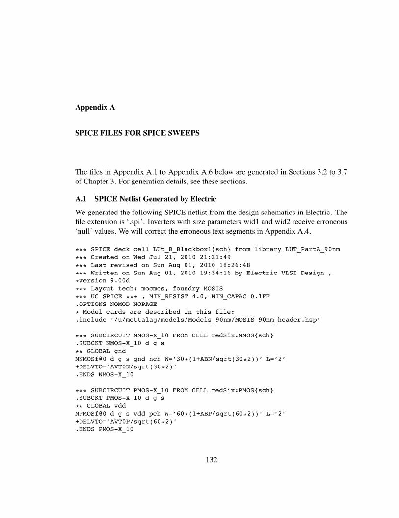
Appendix A
SPICE FILES FOR SPICE SWEEPS
The files in Appendix A.1 to Appendix A.6 below are generated in Sections 3.2 to 3.7of Chapter 3. For generation details, see these sections.
A.1 SPICE Netlist Generated by Electric
We generated the following SPICE netlist from the design schematics in Electric. Thefile extension is ‘.spi’. Inverters with size parameters wid1 and wid2 receive erroneous‘null’ values. We will correct the erroneous text segments in Appendix A.4.
*** SPICE deck cell LUt_B_Blackbox1{sch} from library LUT_PartA_90nm*** Created on Wed Jul 21, 2010 21:21:49
*** Last revised on Sun Aug 01, 2010 18:26:48
*** Written on Sun Aug 01, 2010 19:34:16 by Electric VLSI Design ,*version 9.00d
*** Layout tech: mocmos, foundry MOSIS*** UC SPICE *** , MIN_RESIST 4.0, MIN_CAPAC 0.1FF.OPTIONS NOMOD NOPAGE
* Model cards are described in this file:.include ’/u/mettalag/models/Models_90nm/MOSIS_90nm_header.hsp’
*** SUBCIRCUIT NMOS-X_10 FROM CELL redSix:NMOS{sch}.SUBCKT NMOS-X_10 d g s
** GLOBAL gndMNMOSf@0 d g s gnd nch W=’30*(1+ABN/sqrt(30*2))’ L=’2’+DELVTO=’AVT0N/sqrt(30*2)’.ENDS NMOS-X_10
*** SUBCIRCUIT PMOS-X_10 FROM CELL redSix:PMOS{sch}.SUBCKT PMOS-X_10 d g s** GLOBAL vddMPMOSf@0 d g s vdd pch W=’60*(1+ABP/sqrt(60*2))’ L=’2’+DELVTO=’AVT0P/sqrt(60*2)’.ENDS PMOS-X_10
132
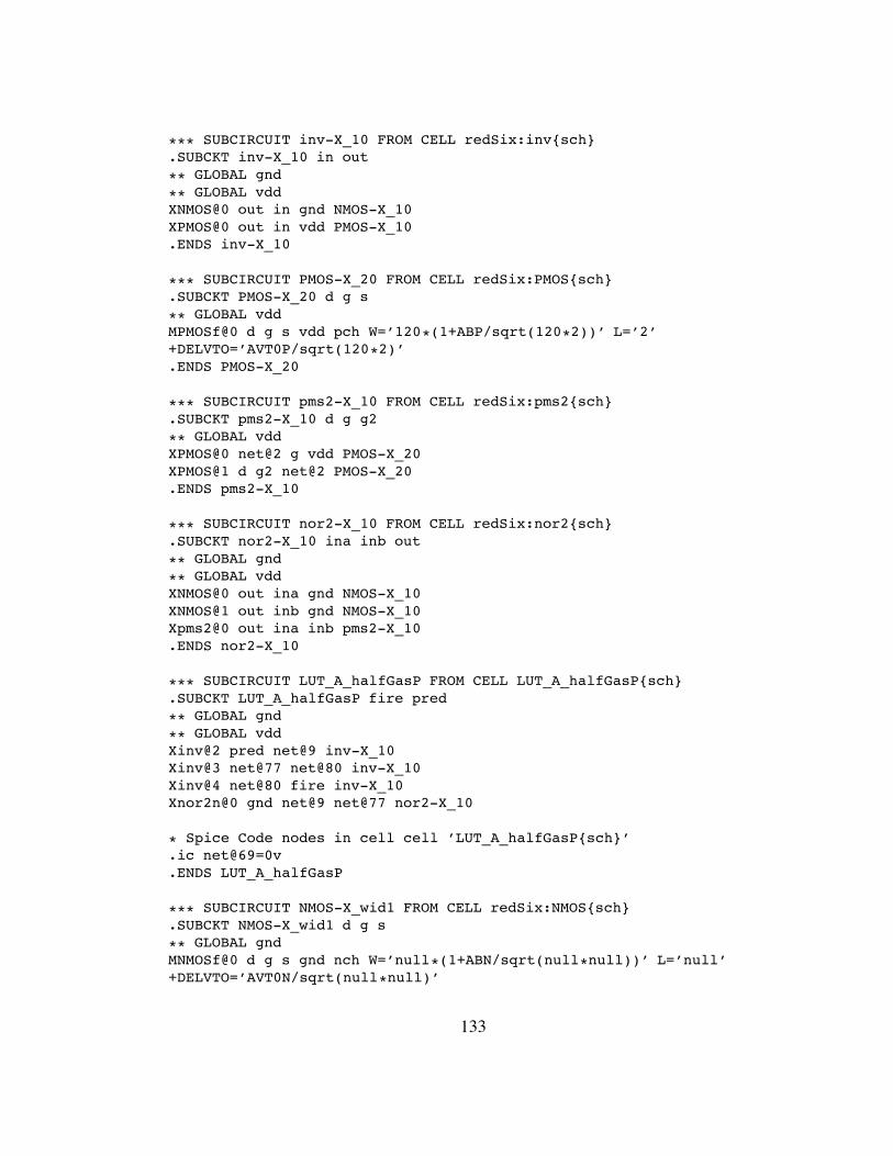
*** SUBCIRCUIT inv-X_10 FROM CELL redSix:inv{sch}.SUBCKT inv-X_10 in out
** GLOBAL gnd
** GLOBAL vddXNMOS@0 out in gnd NMOS-X_10XPMOS@0 out in vdd PMOS-X_10.ENDS inv-X_10
*** SUBCIRCUIT PMOS-X_20 FROM CELL redSix:PMOS{sch}.SUBCKT PMOS-X_20 d g s
** GLOBAL vddMPMOSf@0 d g s vdd pch W=’120*(1+ABP/sqrt(120*2))’ L=’2’+DELVTO=’AVT0P/sqrt(120*2)’.ENDS PMOS-X_20
*** SUBCIRCUIT pms2-X_10 FROM CELL redSix:pms2{sch}.SUBCKT pms2-X_10 d g g2** GLOBAL vddXPMOS@0 net@2 g vdd PMOS-X_20XPMOS@1 d g2 net@2 PMOS-X_20.ENDS pms2-X_10
*** SUBCIRCUIT nor2-X_10 FROM CELL redSix:nor2{sch}.SUBCKT nor2-X_10 ina inb out
** GLOBAL gnd** GLOBAL vddXNMOS@0 out ina gnd NMOS-X_10XNMOS@1 out inb gnd NMOS-X_10Xpms2@0 out ina inb pms2-X_10.ENDS nor2-X_10
*** SUBCIRCUIT LUT_A_halfGasP FROM CELL LUT_A_halfGasP{sch}.SUBCKT LUT_A_halfGasP fire pred** GLOBAL gnd
** GLOBAL vddXinv@2 pred net@9 inv-X_10Xinv@3 net@77 net@80 inv-X_10Xinv@4 net@80 fire inv-X_10Xnor2n@0 gnd net@9 net@77 nor2-X_10
* Spice Code nodes in cell cell ’LUT_A_halfGasP{sch}’.ic net@69=0v.ENDS LUT_A_halfGasP
*** SUBCIRCUIT NMOS-X_wid1 FROM CELL redSix:NMOS{sch}.SUBCKT NMOS-X_wid1 d g s** GLOBAL gndMNMOSf@0 d g s gnd nch W=’null*(1+ABN/sqrt(null*null))’ L=’null’+DELVTO=’AVT0N/sqrt(null*null)’
133
.ENDS NMOS-X_wid1
*** SUBCIRCUIT PMOS-X_wid1 FROM CELL redSix:PMOS{sch}.SUBCKT PMOS-X_wid1 d g s** GLOBAL vddMPMOSf@0 d g s vdd pch W=’null*(1+ABP/sqrt(null*null))’ L=’null’+DELVTO=’AVT0P/sqrt(null*null)’.ENDS PMOS-X_wid1
*** SUBCIRCUIT inv-X_wid1 FROM CELL redSix:inv{sch}.SUBCKT inv-X_wid1 in out
** GLOBAL gnd** GLOBAL vddXNMOS@0 out in gnd NMOS-X_wid1XPMOS@0 out in vdd PMOS-X_wid1.ENDS inv-X_wid1
*** SUBCIRCUIT NMOS-X_wids FROM CELL redSix:NMOS{sch}.SUBCKT NMOS-X_wids d g s
** GLOBAL gndMNMOSf@0 d g s gnd nch W=’null*(1+ABN/sqrt(null*null))’ L=’null’+DELVTO=’AVT0N/sqrt(null*null)’.ENDS NMOS-X_wids
*** SUBCIRCUIT PMOS-X_wids FROM CELL redSix:PMOS{sch}.SUBCKT PMOS-X_wids d g s
** GLOBAL vddMPMOSf@0 d g s vdd pch W=’null*(1+ABP/sqrt(null*null))’ L=’null’+DELVTO=’AVT0P/sqrt(null*null)’.ENDS PMOS-X_wids
*** SUBCIRCUIT inv-X_wids FROM CELL redSix:inv{sch}.SUBCKT inv-X_wids in out** GLOBAL gnd
** GLOBAL vddXNMOS@0 out in gnd NMOS-X_widsXPMOS@0 out in vdd PMOS-X_wids.ENDS inv-X_wids
*** SUBCIRCUIT NMOS-X_widM FROM CELL redSix:NMOS{sch}.SUBCKT NMOS-X_widM d g s** GLOBAL gndMNMOSf@0 d g s gnd nch W=’null*(1+ABN/sqrt(null*null))’ L=’null’+DELVTO=’AVT0N/sqrt(null*null)’.ENDS NMOS-X_widM
*** SUBCIRCUIT PMOS-X_widM FROM CELL redSix:PMOS{sch}.SUBCKT PMOS-X_widM d g s
** GLOBAL vdd
134
MPMOSf@0 d g s vdd pch W=’null*(1+ABP/sqrt(null*null))’ L=’null’+DELVTO=’AVT0P/sqrt(null*null)’.ENDS PMOS-X_widM
*** SUBCIRCUIT inv-X_widM FROM CELL redSix:inv{sch}.SUBCKT inv-X_widM in out** GLOBAL gnd
** GLOBAL vddXNMOS@0 out in gnd NMOS-X_widMXPMOS@0 out in vdd PMOS-X_widM.ENDS inv-X_widM
*** SUBCIRCUIT NMOS-X_wid2 FROM CELL redSix:NMOS{sch}.SUBCKT NMOS-X_wid2 d g s** GLOBAL gndMNMOSf@0 d g s gnd nch W=’null*(1+ABN/sqrt(null*null))’ L=’null’+DELVTO=’AVT0N/sqrt(null*null)’.ENDS NMOS-X_wid2
*** SUBCIRCUIT PMOS-X_wid2 FROM CELL redSix:PMOS{sch}.SUBCKT PMOS-X_wid2 d g s
** GLOBAL vddMPMOSf@0 d g s vdd pch W=’null*(1+ABP/sqrt(null*null))’ L=’null’+DELVTO=’AVT0P/sqrt(null*null)’.ENDS PMOS-X_wid2
*** SUBCIRCUIT inv-X_wid2 FROM CELL redSix:inv{sch}.SUBCKT inv-X_wid2 in out** GLOBAL gnd
** GLOBAL vddXNMOS@0 out in gnd NMOS-X_wid2XPMOS@0 out in vdd PMOS-X_wid2.ENDS inv-X_wid2
.global gnd vdd
*** TOP LEVEL CELL: LUt_B_Blackbox1{sch}XLUT_A_ha@0 out[1] in[1] LUT_A_halfGasPVPulse@0 net@139 gnd pulse 0 ’1v’ ’0ns’ ’50ps’ ’50ps’ ’2ns’ ’4ns’Xinv@1 Din[1] in[1] inv-X_wid1Xinv@2 net@139 Din[1] inv-X_widsXinv@3 net@64 inv@3_out inv-X_widMXinv@4 out[1] net@64 inv-X_wid2
* Trailer cards are described in this file:.include ’/u/mettalag/models/Models_90nm/MOSIS_90nm_trailer.hsp’.END
135
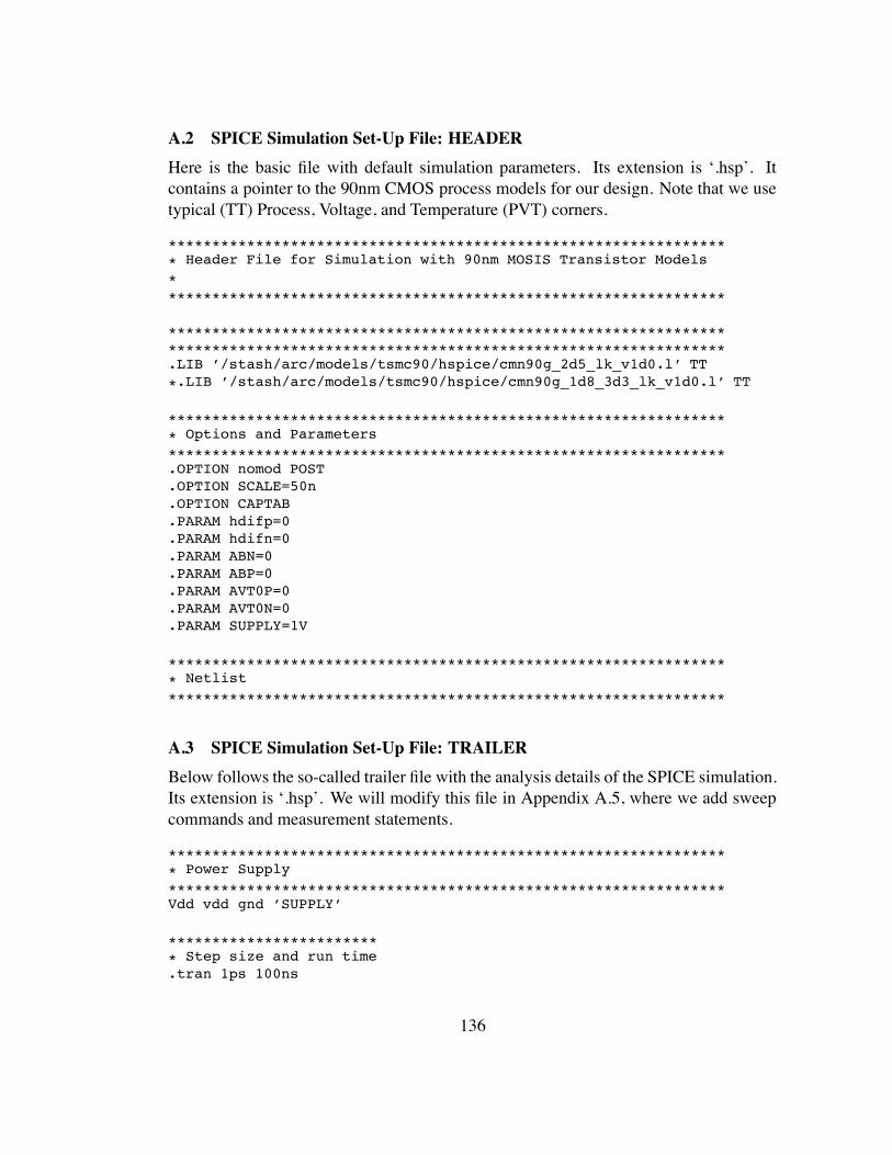
A.2 SPICE Simulation Set-Up File: HEADERHere is the basic file with default simulation parameters. Its extension is ‘.hsp’. Itcontains a pointer to the 90nm CMOS process models for our design. Note that we usetypical (TT) Process, Voltage, and Temperature (PVT) corners.
***************************************************************** Header File for Simulation with 90nm MOSIS Transistor Models
*****************************************************************
********************************************************************************************************************************.LIB ’/stash/arc/models/tsmc90/hspice/cmn90g_2d5_lk_v1d0.l’ TT
*.LIB ’/stash/arc/models/tsmc90/hspice/cmn90g_1d8_3d3_lk_v1d0.l’ TT
***************************************************************** Options and Parameters****************************************************************.OPTION nomod POST.OPTION SCALE=50n.OPTION CAPTAB.PARAM hdifp=0.PARAM hdifn=0.PARAM ABN=0.PARAM ABP=0.PARAM AVT0P=0.PARAM AVT0N=0.PARAM SUPPLY=1V
***************************************************************** Netlist
****************************************************************
A.3 SPICE Simulation Set-Up File: TRAILERBelow follows the so-called trailer file with the analysis details of the SPICE simulation.Its extension is ‘.hsp’. We will modify this file in Appendix A.5, where we add sweepcommands and measurement statements.
***************************************************************** Power Supply
****************************************************************Vdd vdd gnd ’SUPPLY’
************************* Step size and run time.tran 1ps 100ns
136
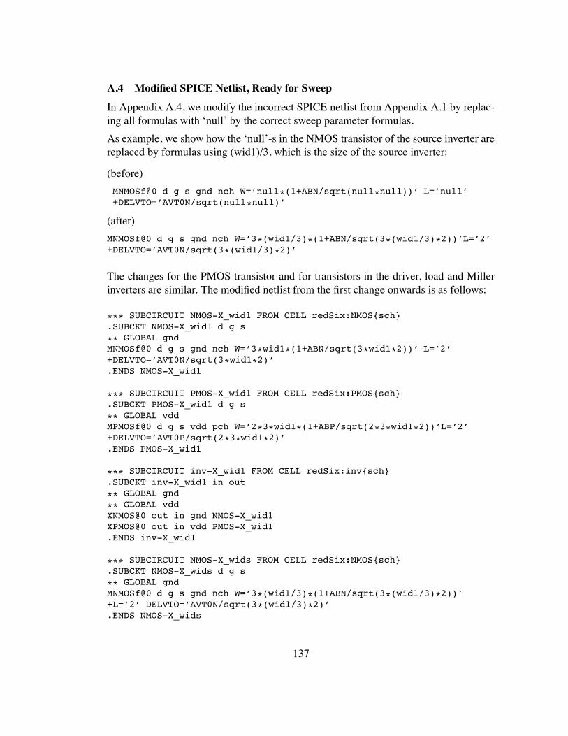
A.4 Modified SPICE Netlist, Ready for SweepIn Appendix A.4, we modify the incorrect SPICE netlist from Appendix A.1 by replac-ing all formulas with ‘null’ by the correct sweep parameter formulas.As example, we show how the ‘null’-s in the NMOS transistor of the source inverter arereplaced by formulas using (wid1)/3, which is the size of the source inverter:
(before)MNMOSf@0 d g s gnd nch W=’null*(1+ABN/sqrt(null*null))’ L=’null’+DELVTO=’AVT0N/sqrt(null*null)’
(after)MNMOSf@0 d g s gnd nch W=’3*(wid1/3)*(1+ABN/sqrt(3*(wid1/3)*2))’L=’2’+DELVTO=’AVT0N/sqrt(3*(wid1/3)*2)’
The changes for the PMOS transistor and for transistors in the driver, load and Millerinverters are similar. The modified netlist from the first change onwards is as follows:
*** SUBCIRCUIT NMOS-X_wid1 FROM CELL redSix:NMOS{sch}.SUBCKT NMOS-X_wid1 d g s
** GLOBAL gndMNMOSf@0 d g s gnd nch W=’3*wid1*(1+ABN/sqrt(3*wid1*2))’ L=’2’+DELVTO=’AVT0N/sqrt(3*wid1*2)’.ENDS NMOS-X_wid1
*** SUBCIRCUIT PMOS-X_wid1 FROM CELL redSix:PMOS{sch}.SUBCKT PMOS-X_wid1 d g s
** GLOBAL vddMPMOSf@0 d g s vdd pch W=’2*3*wid1*(1+ABP/sqrt(2*3*wid1*2))’L=’2’+DELVTO=’AVT0P/sqrt(2*3*wid1*2)’.ENDS PMOS-X_wid1
*** SUBCIRCUIT inv-X_wid1 FROM CELL redSix:inv{sch}.SUBCKT inv-X_wid1 in out** GLOBAL gnd
** GLOBAL vddXNMOS@0 out in gnd NMOS-X_wid1XPMOS@0 out in vdd PMOS-X_wid1.ENDS inv-X_wid1
*** SUBCIRCUIT NMOS-X_wids FROM CELL redSix:NMOS{sch}.SUBCKT NMOS-X_wids d g s** GLOBAL gndMNMOSf@0 d g s gnd nch W=’3*(wid1/3)*(1+ABN/sqrt(3*(wid1/3)*2))’+L=’2’ DELVTO=’AVT0N/sqrt(3*(wid1/3)*2)’.ENDS NMOS-X_wids
137
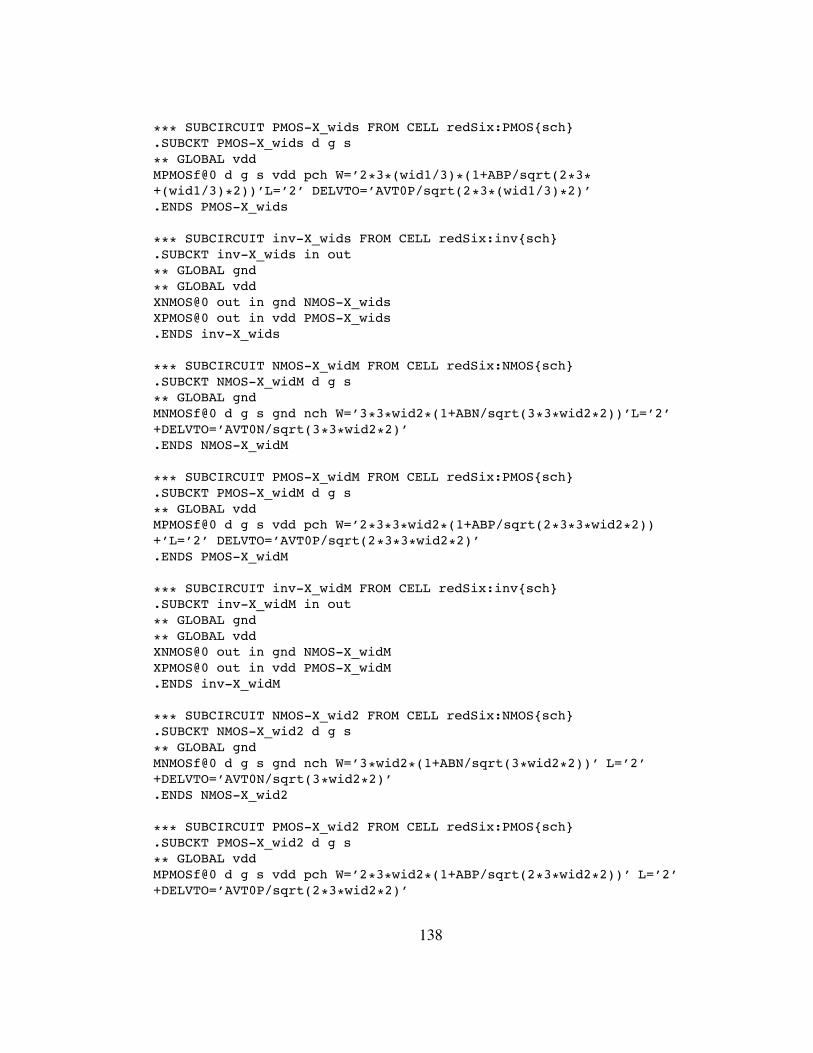
*** SUBCIRCUIT PMOS-X_wids FROM CELL redSix:PMOS{sch}.SUBCKT PMOS-X_wids d g s
** GLOBAL vddMPMOSf@0 d g s vdd pch W=’2*3*(wid1/3)*(1+ABP/sqrt(2*3*+(wid1/3)*2))’L=’2’ DELVTO=’AVT0P/sqrt(2*3*(wid1/3)*2)’.ENDS PMOS-X_wids
*** SUBCIRCUIT inv-X_wids FROM CELL redSix:inv{sch}.SUBCKT inv-X_wids in out** GLOBAL gnd
** GLOBAL vddXNMOS@0 out in gnd NMOS-X_widsXPMOS@0 out in vdd PMOS-X_wids.ENDS inv-X_wids
*** SUBCIRCUIT NMOS-X_widM FROM CELL redSix:NMOS{sch}.SUBCKT NMOS-X_widM d g s** GLOBAL gndMNMOSf@0 d g s gnd nch W=’3*3*wid2*(1+ABN/sqrt(3*3*wid2*2))’L=’2’+DELVTO=’AVT0N/sqrt(3*3*wid2*2)’.ENDS NMOS-X_widM
*** SUBCIRCUIT PMOS-X_widM FROM CELL redSix:PMOS{sch}.SUBCKT PMOS-X_widM d g s
** GLOBAL vddMPMOSf@0 d g s vdd pch W=’2*3*3*wid2*(1+ABP/sqrt(2*3*3*wid2*2))+’L=’2’ DELVTO=’AVT0P/sqrt(2*3*3*wid2*2)’.ENDS PMOS-X_widM
*** SUBCIRCUIT inv-X_widM FROM CELL redSix:inv{sch}.SUBCKT inv-X_widM in out
** GLOBAL gnd
** GLOBAL vddXNMOS@0 out in gnd NMOS-X_widMXPMOS@0 out in vdd PMOS-X_widM.ENDS inv-X_widM
*** SUBCIRCUIT NMOS-X_wid2 FROM CELL redSix:NMOS{sch}.SUBCKT NMOS-X_wid2 d g s
** GLOBAL gndMNMOSf@0 d g s gnd nch W=’3*wid2*(1+ABN/sqrt(3*wid2*2))’ L=’2’+DELVTO=’AVT0N/sqrt(3*wid2*2)’.ENDS NMOS-X_wid2
*** SUBCIRCUIT PMOS-X_wid2 FROM CELL redSix:PMOS{sch}.SUBCKT PMOS-X_wid2 d g s** GLOBAL vddMPMOSf@0 d g s vdd pch W=’2*3*wid2*(1+ABP/sqrt(2*3*wid2*2))’ L=’2’+DELVTO=’AVT0P/sqrt(2*3*wid2*2)’
138
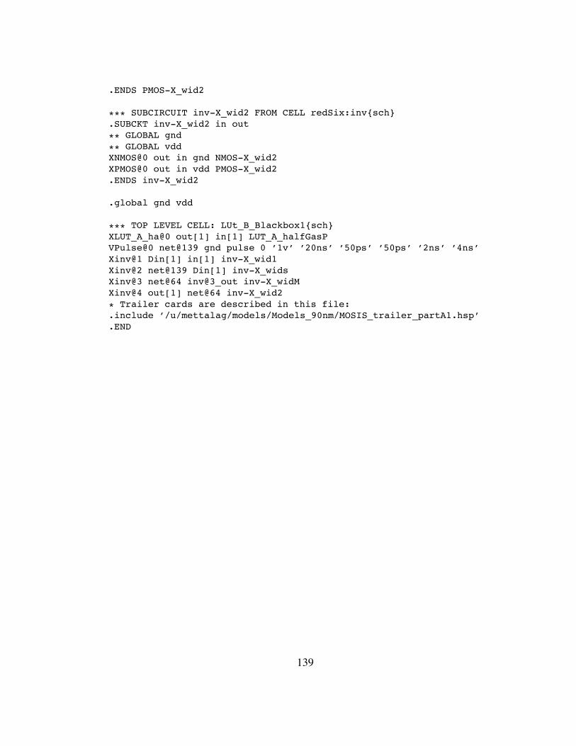
.ENDS PMOS-X_wid2
*** SUBCIRCUIT inv-X_wid2 FROM CELL redSix:inv{sch}.SUBCKT inv-X_wid2 in out** GLOBAL gnd
** GLOBAL vddXNMOS@0 out in gnd NMOS-X_wid2XPMOS@0 out in vdd PMOS-X_wid2.ENDS inv-X_wid2
.global gnd vdd
*** TOP LEVEL CELL: LUt_B_Blackbox1{sch}XLUT_A_ha@0 out[1] in[1] LUT_A_halfGasPVPulse@0 net@139 gnd pulse 0 ’1v’ ’20ns’ ’50ps’ ’50ps’ ’2ns’ ’4ns’Xinv@1 Din[1] in[1] inv-X_wid1Xinv@2 net@139 Din[1] inv-X_widsXinv@3 net@64 inv@3_out inv-X_widMXinv@4 out[1] net@64 inv-X_wid2
* Trailer cards are described in this file:.include ’/u/mettalag/models/Models_90nm/MOSIS_trailer_partA1.hsp’.END
139
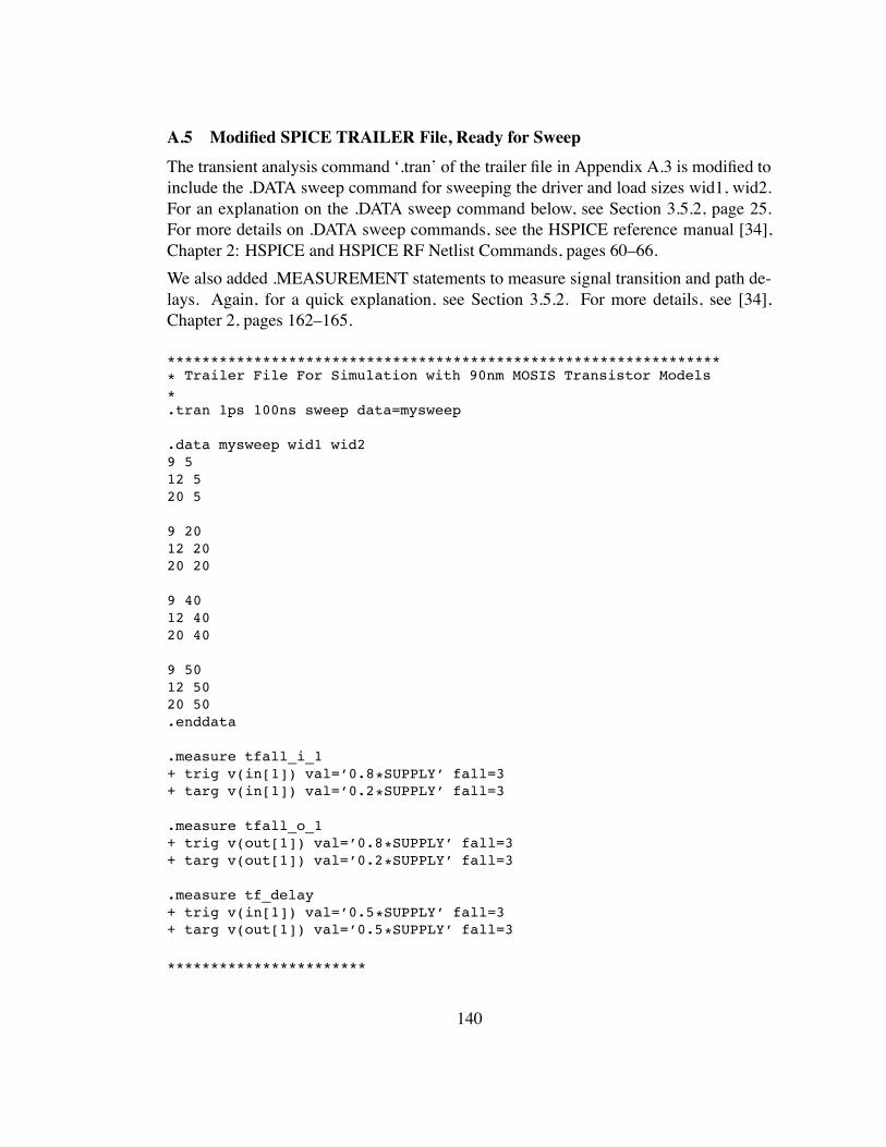
A.5 Modified SPICE TRAILER File, Ready for SweepThe transient analysis command ‘.tran’ of the trailer file in Appendix A.3 is modified toinclude the .DATA sweep command for sweeping the driver and load sizes wid1, wid2.For an explanation on the .DATA sweep command below, see Section 3.5.2, page 25.For more details on .DATA sweep commands, see the HSPICE reference manual [34],Chapter 2: HSPICE and HSPICE RF Netlist Commands, pages 60–66.We also added .MEASUREMENT statements to measure signal transition and path de-lays. Again, for a quick explanation, see Section 3.5.2. For more details, see [34],Chapter 2, pages 162–165.
***************************************************************** Trailer File For Simulation with 90nm MOSIS Transistor Models
*.tran 1ps 100ns sweep data=mysweep
.data mysweep wid1 wid29 512 520 5
9 2012 2020 20
9 4012 4020 40
9 5012 5020 50.enddata
.measure tfall_i_1+ trig v(in[1]) val=’0.8*SUPPLY’ fall=3+ targ v(in[1]) val=’0.2*SUPPLY’ fall=3
.measure tfall_o_1+ trig v(out[1]) val=’0.8*SUPPLY’ fall=3+ targ v(out[1]) val=’0.2*SUPPLY’ fall=3
.measure tf_delay+ trig v(in[1]) val=’0.5*SUPPLY’ fall=3+ targ v(out[1]) val=’0.5*SUPPLY’ fall=3
***********************
140
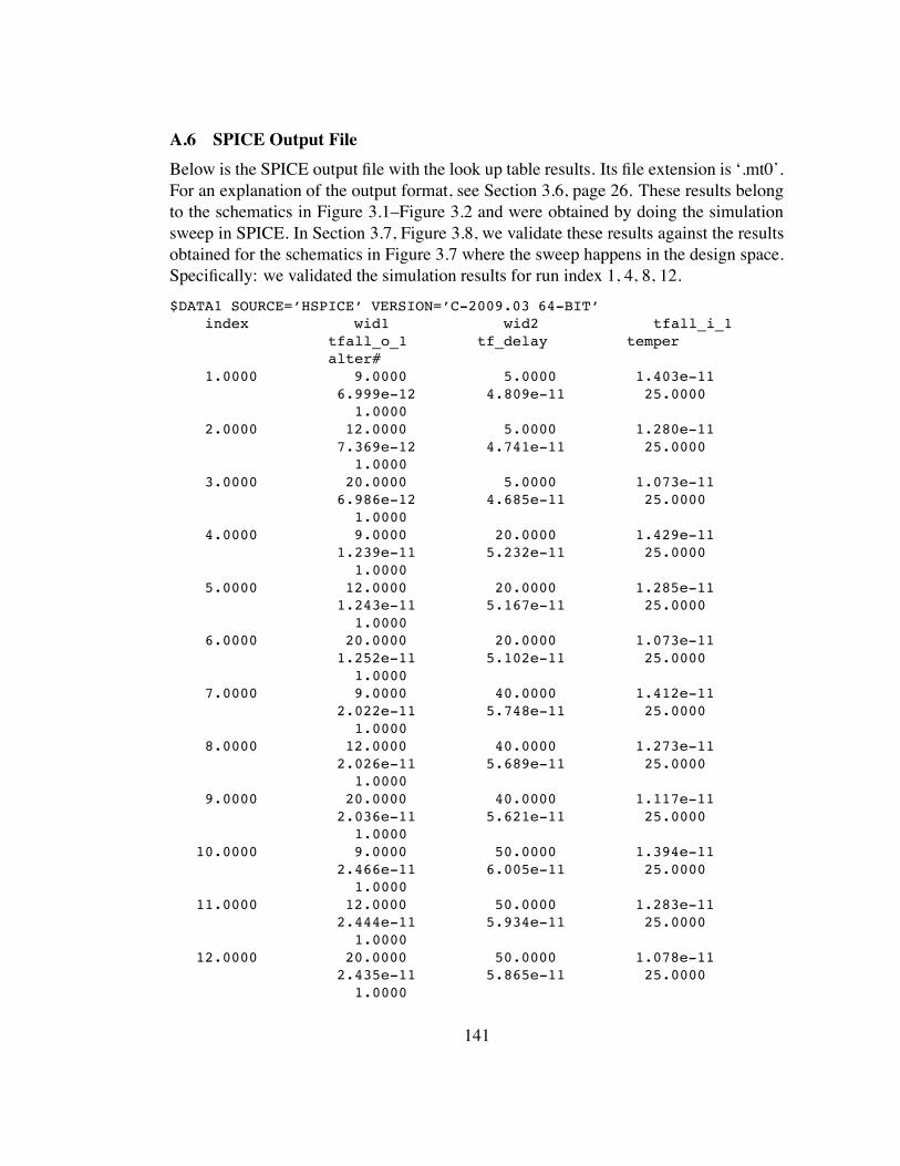
A.6 SPICE Output FileBelow is the SPICE output file with the look up table results. Its file extension is ‘.mt0’.For an explanation of the output format, see Section 3.6, page 26. These results belongto the schematics in Figure 3.1–Figure 3.2 and were obtained by doing the simulationsweep in SPICE. In Section 3.7, Figure 3.8, we validate these results against the resultsobtained for the schematics in Figure 3.7 where the sweep happens in the design space.Specifically: we validated the simulation results for run index 1, 4, 8, 12.$DATA1 SOURCE=’HSPICE’ VERSION=’C-2009.03 64-BIT’
index wid1 wid2 tfall_i_1tfall_o_1 tf_delay temperalter#
1.0000 9.0000 5.0000 1.403e-116.999e-12 4.809e-11 25.0000
1.00002.0000 12.0000 5.0000 1.280e-11
7.369e-12 4.741e-11 25.00001.0000
3.0000 20.0000 5.0000 1.073e-116.986e-12 4.685e-11 25.0000
1.00004.0000 9.0000 20.0000 1.429e-11
1.239e-11 5.232e-11 25.00001.0000
5.0000 12.0000 20.0000 1.285e-111.243e-11 5.167e-11 25.0000
1.00006.0000 20.0000 20.0000 1.073e-11
1.252e-11 5.102e-11 25.00001.0000
7.0000 9.0000 40.0000 1.412e-112.022e-11 5.748e-11 25.0000
1.00008.0000 12.0000 40.0000 1.273e-11
2.026e-11 5.689e-11 25.00001.0000
9.0000 20.0000 40.0000 1.117e-112.036e-11 5.621e-11 25.0000
1.000010.0000 9.0000 50.0000 1.394e-11
2.466e-11 6.005e-11 25.00001.0000
11.0000 12.0000 50.0000 1.283e-112.444e-11 5.934e-11 25.0000
1.000012.0000 20.0000 50.0000 1.078e-11
2.435e-11 5.865e-11 25.00001.0000
141
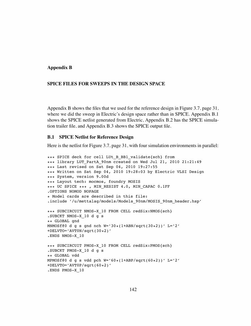
Appendix B
SPICE FILES FOR SWEEPS IN THE DESIGN SPACE
Appendix B shows the files that we used for the reference design in Figure 3.7, page 31,where we did the sweep in Electric’s design space rather than in SPICE. Appendix B.1shows the SPICE netlist generated from Electric, Appendix B.2 has the SPICE simula-tion trailer file, and Appendix B.3 shows the SPICE output file.
B.1 SPICE Netlist for Reference Design
Here is the netlist for Figure 3.7, page 31, with four simulation environments in parallel:
*** SPICE deck for cell LUt_B_BB1_validate{sch} from*** library LUT_PartA_90nm created on Wed Jul 21, 2010 21:21:49
*** Last revised on Sat Sep 04, 2010 19:27:55
*** Written on Sat Sep 04, 2010 19:28:03 by Electric VLSI Design*** System, version 9.00d
*** Layout tech: mocmos, foundry MOSIS*** UC SPICE *** , MIN_RESIST 4.0, MIN_CAPAC 0.1FF.OPTIONS NOMOD NOPAGE
* Model cards are described in this file:.include ’/u/mettalag/models/Models_90nm/MOSIS_90nm_header.hsp’
*** SUBCIRCUIT NMOS-X_10 FROM CELL redSix:NMOS{sch}.SUBCKT NMOS-X_10 d g s
** GLOBAL gndMNMOSf@0 d g s gnd nch W=’30*(1+ABN/sqrt(30*2))’ L=’2’+DELVTO=’AVT0N/sqrt(30*2)’.ENDS NMOS-X_10
*** SUBCIRCUIT PMOS-X_10 FROM CELL redSix:PMOS{sch}.SUBCKT PMOS-X_10 d g s** GLOBAL vddMPMOSf@0 d g s vdd pch W=’60*(1+ABP/sqrt(60*2))’ L=’2’+DELVTO=’AVT0P/sqrt(60*2)’.ENDS PMOS-X_10
142
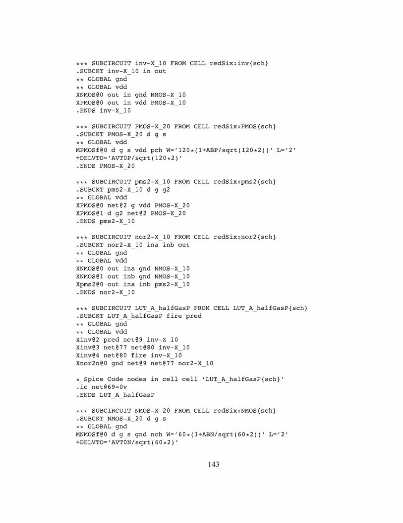
*** SUBCIRCUIT inv-X_10 FROM CELL redSix:inv{sch}.SUBCKT inv-X_10 in out
** GLOBAL gnd
** GLOBAL vddXNMOS@0 out in gnd NMOS-X_10XPMOS@0 out in vdd PMOS-X_10.ENDS inv-X_10
*** SUBCIRCUIT PMOS-X_20 FROM CELL redSix:PMOS{sch}.SUBCKT PMOS-X_20 d g s
** GLOBAL vddMPMOSf@0 d g s vdd pch W=’120*(1+ABP/sqrt(120*2))’ L=’2’+DELVTO=’AVT0P/sqrt(120*2)’.ENDS PMOS-X_20
*** SUBCIRCUIT pms2-X_10 FROM CELL redSix:pms2{sch}.SUBCKT pms2-X_10 d g g2** GLOBAL vddXPMOS@0 net@2 g vdd PMOS-X_20XPMOS@1 d g2 net@2 PMOS-X_20.ENDS pms2-X_10
*** SUBCIRCUIT nor2-X_10 FROM CELL redSix:nor2{sch}.SUBCKT nor2-X_10 ina inb out
** GLOBAL gnd** GLOBAL vddXNMOS@0 out ina gnd NMOS-X_10XNMOS@1 out inb gnd NMOS-X_10Xpms2@0 out ina inb pms2-X_10.ENDS nor2-X_10
*** SUBCIRCUIT LUT_A_halfGasP FROM CELL LUT_A_halfGasP{sch}.SUBCKT LUT_A_halfGasP fire pred** GLOBAL gnd
** GLOBAL vddXinv@2 pred net@9 inv-X_10Xinv@3 net@77 net@80 inv-X_10Xinv@4 net@80 fire inv-X_10Xnor2n@0 gnd net@9 net@77 nor2-X_10
* Spice Code nodes in cell cell ’LUT_A_halfGasP{sch}’.ic net@69=0v.ENDS LUT_A_halfGasP
*** SUBCIRCUIT NMOS-X_20 FROM CELL redSix:NMOS{sch}.SUBCKT NMOS-X_20 d g s** GLOBAL gndMNMOSf@0 d g s gnd nch W=’60*(1+ABN/sqrt(60*2))’ L=’2’+DELVTO=’AVT0N/sqrt(60*2)’
143
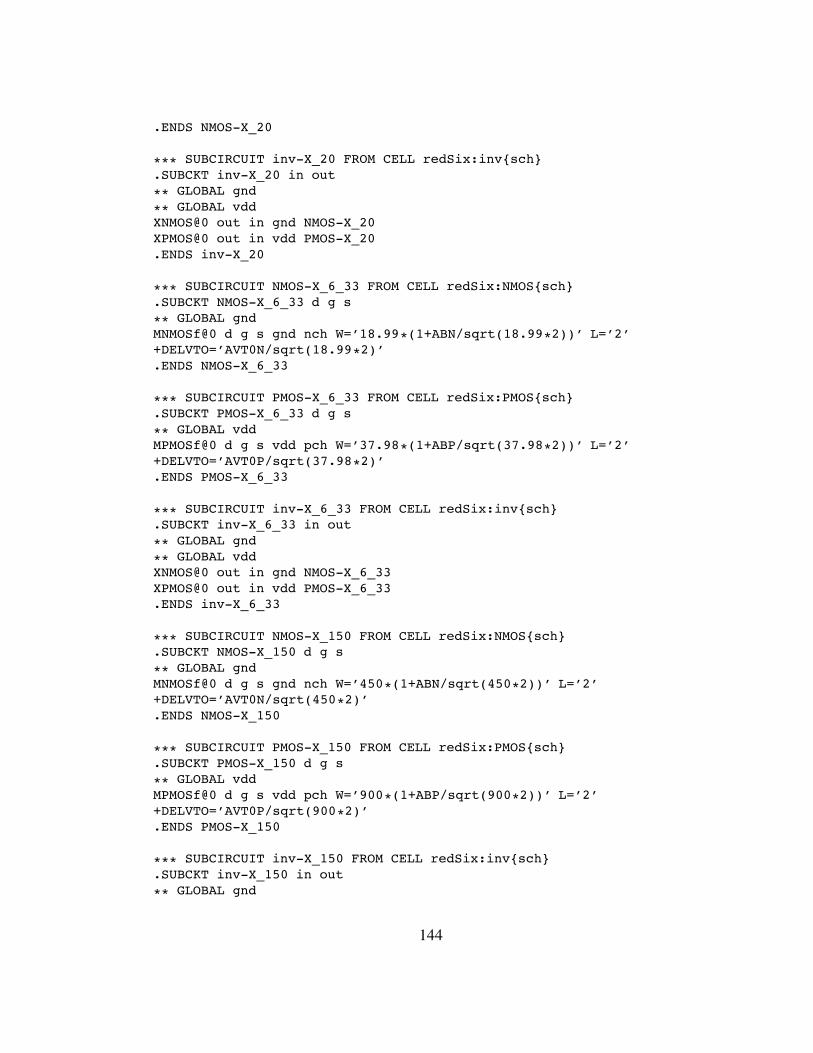
.ENDS NMOS-X_20
*** SUBCIRCUIT inv-X_20 FROM CELL redSix:inv{sch}.SUBCKT inv-X_20 in out** GLOBAL gnd
** GLOBAL vddXNMOS@0 out in gnd NMOS-X_20XPMOS@0 out in vdd PMOS-X_20.ENDS inv-X_20
*** SUBCIRCUIT NMOS-X_6_33 FROM CELL redSix:NMOS{sch}.SUBCKT NMOS-X_6_33 d g s** GLOBAL gndMNMOSf@0 d g s gnd nch W=’18.99*(1+ABN/sqrt(18.99*2))’ L=’2’+DELVTO=’AVT0N/sqrt(18.99*2)’.ENDS NMOS-X_6_33
*** SUBCIRCUIT PMOS-X_6_33 FROM CELL redSix:PMOS{sch}.SUBCKT PMOS-X_6_33 d g s
** GLOBAL vddMPMOSf@0 d g s vdd pch W=’37.98*(1+ABP/sqrt(37.98*2))’ L=’2’+DELVTO=’AVT0P/sqrt(37.98*2)’.ENDS PMOS-X_6_33
*** SUBCIRCUIT inv-X_6_33 FROM CELL redSix:inv{sch}.SUBCKT inv-X_6_33 in out
** GLOBAL gnd
** GLOBAL vddXNMOS@0 out in gnd NMOS-X_6_33XPMOS@0 out in vdd PMOS-X_6_33.ENDS inv-X_6_33
*** SUBCIRCUIT NMOS-X_150 FROM CELL redSix:NMOS{sch}.SUBCKT NMOS-X_150 d g s
** GLOBAL gndMNMOSf@0 d g s gnd nch W=’450*(1+ABN/sqrt(450*2))’ L=’2’+DELVTO=’AVT0N/sqrt(450*2)’.ENDS NMOS-X_150
*** SUBCIRCUIT PMOS-X_150 FROM CELL redSix:PMOS{sch}.SUBCKT PMOS-X_150 d g s** GLOBAL vddMPMOSf@0 d g s vdd pch W=’900*(1+ABP/sqrt(900*2))’ L=’2’+DELVTO=’AVT0P/sqrt(900*2)’.ENDS PMOS-X_150
*** SUBCIRCUIT inv-X_150 FROM CELL redSix:inv{sch}.SUBCKT inv-X_150 in out
** GLOBAL gnd
144
** GLOBAL vddXNMOS@0 out in gnd NMOS-X_150XPMOS@0 out in vdd PMOS-X_150.ENDS inv-X_150
*** SUBCIRCUIT NMOS-X_50 FROM CELL redSix:NMOS{sch}.SUBCKT NMOS-X_50 d g s
** GLOBAL gndMNMOSf@0 d g s gnd nch W=’150*(1+ABN/sqrt(150*2))’ L=’2’+DELVTO=’AVT0N/sqrt(150*2)’.ENDS NMOS-X_50
*** SUBCIRCUIT PMOS-X_50 FROM CELL redSix:PMOS{sch}.SUBCKT PMOS-X_50 d g s** GLOBAL vddMPMOSf@0 d g s vdd pch W=’300*(1+ABP/sqrt(300*2))’ L=’2’+DELVTO=’AVT0P/sqrt(300*2)’.ENDS PMOS-X_50
*** SUBCIRCUIT inv-X_50 FROM CELL redSix:inv{sch}.SUBCKT inv-X_50 in out
** GLOBAL gnd** GLOBAL vddXNMOS@0 out in gnd NMOS-X_50XPMOS@0 out in vdd PMOS-X_50.ENDS inv-X_50
*** SUBCIRCUIT NMOS-X_12 FROM CELL redSix:NMOS{sch}.SUBCKT NMOS-X_12 d g s
** GLOBAL gndMNMOSf@0 d g s gnd nch W=’36*(1+ABN/sqrt(36*2))’ L=’2’+DELVTO=’AVT0N/sqrt(36*2)’.ENDS NMOS-X_12
*** SUBCIRCUIT PMOS-X_12 FROM CELL redSix:PMOS{sch}.SUBCKT PMOS-X_12 d g s** GLOBAL vddMPMOSf@0 d g s vdd pch W=’72*(1+ABP/sqrt(72*2))’ L=’2’+DELVTO=’AVT0P/sqrt(72*2)’.ENDS PMOS-X_12
*** SUBCIRCUIT inv-X_12 FROM CELL redSix:inv{sch}.SUBCKT inv-X_12 in out
** GLOBAL gnd** GLOBAL vddXNMOS@0 out in gnd NMOS-X_12XPMOS@0 out in vdd PMOS-X_12.ENDS inv-X_12
145
*** SUBCIRCUIT NMOS-X_4 FROM CELL redSix:NMOS{sch}.SUBCKT NMOS-X_4 d g s
** GLOBAL gndMNMOSf@0 d g s gnd nch W=’12*(1+ABN/sqrt(12*2))’ L=’2’+DELVTO=’AVT0N/sqrt(12*2)’.ENDS NMOS-X_4
*** SUBCIRCUIT PMOS-X_4 FROM CELL redSix:PMOS{sch}.SUBCKT PMOS-X_4 d g s** GLOBAL vddMPMOSf@0 d g s vdd pch W=’24*(1+ABP/sqrt(24*2))’ L=’2’+DELVTO=’AVT0P/sqrt(24*2)’.ENDS PMOS-X_4
*** SUBCIRCUIT inv-X_4 FROM CELL redSix:inv{sch}.SUBCKT inv-X_4 in out
** GLOBAL gnd** GLOBAL vddXNMOS@0 out in gnd NMOS-X_4XPMOS@0 out in vdd PMOS-X_4.ENDS inv-X_4
*** SUBCIRCUIT NMOS-X_120 FROM CELL redSix:NMOS{sch}.SUBCKT NMOS-X_120 d g s
** GLOBAL gndMNMOSf@0 d g s gnd nch W=’360*(1+ABN/sqrt(360*2))’ L=’2’+DELVTO=’AVT0N/sqrt(360*2)’.ENDS NMOS-X_120
*** SUBCIRCUIT PMOS-X_120 FROM CELL redSix:PMOS{sch}.SUBCKT PMOS-X_120 d g s
** GLOBAL vddMPMOSf@0 d g s vdd pch W=’720*(1+ABP/sqrt(720*2))’ L=’2’+DELVTO=’AVT0P/sqrt(720*2)’.ENDS PMOS-X_120
*** SUBCIRCUIT inv-X_120 FROM CELL redSix:inv{sch}.SUBCKT inv-X_120 in out** GLOBAL gnd
** GLOBAL vddXNMOS@0 out in gnd NMOS-X_120XPMOS@0 out in vdd PMOS-X_120.ENDS inv-X_120
*** SUBCIRCUIT NMOS-X_40 FROM CELL redSix:NMOS{sch}.SUBCKT NMOS-X_40 d g s** GLOBAL gndMNMOSf@0 d g s gnd nch W=’120*(1+ABN/sqrt(120*2))’ L=’2’+DELVTO=’AVT0N/sqrt(120*2)’
146
.ENDS NMOS-X_40
*** SUBCIRCUIT PMOS-X_40 FROM CELL redSix:PMOS{sch}.SUBCKT PMOS-X_40 d g s** GLOBAL vddMPMOSf@0 d g s vdd pch W=’240*(1+ABP/sqrt(240*2))’ L=’2’+DELVTO=’AVT0P/sqrt(240*2)’.ENDS PMOS-X_40
*** SUBCIRCUIT inv-X_40 FROM CELL redSix:inv{sch}.SUBCKT inv-X_40 in out
** GLOBAL gnd** GLOBAL vddXNMOS@0 out in gnd NMOS-X_40XPMOS@0 out in vdd PMOS-X_40.ENDS inv-X_40
*** SUBCIRCUIT NMOS-X_9 FROM CELL redSix:NMOS{sch}.SUBCKT NMOS-X_9 d g s
** GLOBAL gndMNMOSf@0 d g s gnd nch W=’27*(1+ABN/sqrt(27*2))’ L=’2’+DELVTO=’AVT0N/sqrt(27*2)’.ENDS NMOS-X_9
*** SUBCIRCUIT PMOS-X_9 FROM CELL redSix:PMOS{sch}.SUBCKT PMOS-X_9 d g s** GLOBAL vddMPMOSf@0 d g s vdd pch W=’54*(1+ABP/sqrt(54*2))’ L=’2’+DELVTO=’AVT0P/sqrt(54*2)’.ENDS PMOS-X_9
*** SUBCIRCUIT inv-X_9 FROM CELL redSix:inv{sch}.SUBCKT inv-X_9 in out
** GLOBAL gnd** GLOBAL vddXNMOS@0 out in gnd NMOS-X_9XPMOS@0 out in vdd PMOS-X_9.ENDS inv-X_9
*** SUBCIRCUIT NMOS-X_3 FROM CELL redSix:NMOS{sch}.SUBCKT NMOS-X_3 d g s
** GLOBAL gndMNMOSf@0 d g s gnd nch W=’9*(1+ABN/sqrt(9*2))’+L=’2’ DELVTO=’AVT0N/sqrt(9*2)’.ENDS NMOS-X_3
*** SUBCIRCUIT PMOS-X_3 FROM CELL redSix:PMOS{sch}.SUBCKT PMOS-X_3 d g s
** GLOBAL vddMPMOSf@0 d g s vdd pch W=’18*(1+ABP/sqrt(18*2))’ L=’2’
147
+DELVTO=’AVT0P/sqrt(18*2)’.ENDS PMOS-X_3
*** SUBCIRCUIT inv-X_3 FROM CELL redSix:inv{sch}.SUBCKT inv-X_3 in out
** GLOBAL gnd** GLOBAL vddXNMOS@0 out in gnd NMOS-X_3XPMOS@0 out in vdd PMOS-X_3.ENDS inv-X_3
*** SUBCIRCUIT NMOS-X_60 FROM CELL redSix:NMOS{sch}.SUBCKT NMOS-X_60 d g s** GLOBAL gndMNMOSf@0 d g s gnd nch W=’180*(1+ABN/sqrt(180*2))’ L=’2’+DELVTO=’AVT0N/sqrt(180*2)’.ENDS NMOS-X_60
*** SUBCIRCUIT PMOS-X_60 FROM CELL redSix:PMOS{sch}.SUBCKT PMOS-X_60 d g s
** GLOBAL vddMPMOSf@0 d g s vdd pch W=’360*(1+ABP/sqrt(360*2))’ L=’2’+DELVTO=’AVT0P/sqrt(360*2)’.ENDS PMOS-X_60
*** SUBCIRCUIT inv-X_60 FROM CELL redSix:inv{sch}.SUBCKT inv-X_60 in out
** GLOBAL gnd
** GLOBAL vddXNMOS@0 out in gnd NMOS-X_60XPMOS@0 out in vdd PMOS-X_60.ENDS inv-X_60
*** SUBCIRCUIT NMOS-X_15 FROM CELL redSix:NMOS{sch}.SUBCKT NMOS-X_15 d g s
** GLOBAL gndMNMOSf@0 d g s gnd nch W=’45*(1+ABN/sqrt(45*2))’ L=’2’+DELVTO=’AVT0N/sqrt(45*2)’.ENDS NMOS-X_15
*** SUBCIRCUIT PMOS-X_15 FROM CELL redSix:PMOS{sch}.SUBCKT PMOS-X_15 d g s** GLOBAL vddMPMOSf@0 d g s vdd pch W=’90*(1+ABP/sqrt(90*2))’ L=’2’+DELVTO=’AVT0P/sqrt(90*2)’.ENDS PMOS-X_15
*** SUBCIRCUIT inv-X_15 FROM CELL redSix:inv{sch}.SUBCKT inv-X_15 in out
** GLOBAL gnd
148
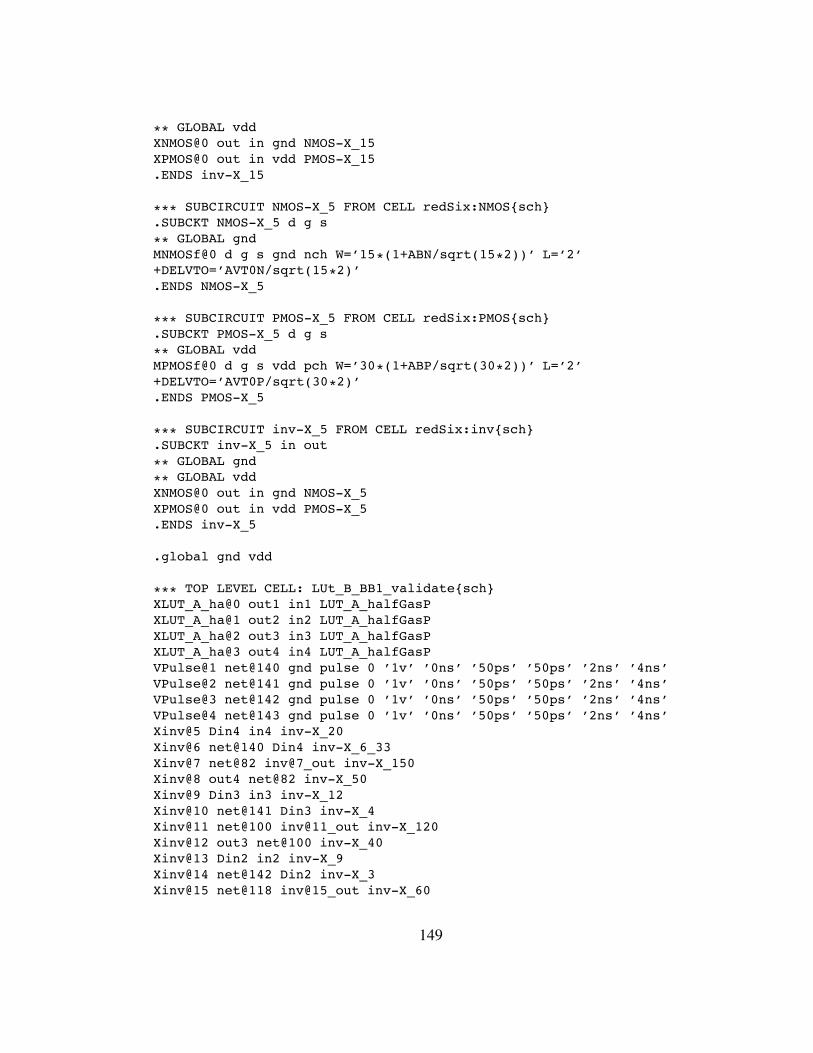
** GLOBAL vddXNMOS@0 out in gnd NMOS-X_15XPMOS@0 out in vdd PMOS-X_15.ENDS inv-X_15
*** SUBCIRCUIT NMOS-X_5 FROM CELL redSix:NMOS{sch}.SUBCKT NMOS-X_5 d g s
** GLOBAL gndMNMOSf@0 d g s gnd nch W=’15*(1+ABN/sqrt(15*2))’ L=’2’+DELVTO=’AVT0N/sqrt(15*2)’.ENDS NMOS-X_5
*** SUBCIRCUIT PMOS-X_5 FROM CELL redSix:PMOS{sch}.SUBCKT PMOS-X_5 d g s** GLOBAL vddMPMOSf@0 d g s vdd pch W=’30*(1+ABP/sqrt(30*2))’ L=’2’+DELVTO=’AVT0P/sqrt(30*2)’.ENDS PMOS-X_5
*** SUBCIRCUIT inv-X_5 FROM CELL redSix:inv{sch}.SUBCKT inv-X_5 in out
** GLOBAL gnd** GLOBAL vddXNMOS@0 out in gnd NMOS-X_5XPMOS@0 out in vdd PMOS-X_5.ENDS inv-X_5
.global gnd vdd
*** TOP LEVEL CELL: LUt_B_BB1_validate{sch}XLUT_A_ha@0 out1 in1 LUT_A_halfGasPXLUT_A_ha@1 out2 in2 LUT_A_halfGasPXLUT_A_ha@2 out3 in3 LUT_A_halfGasPXLUT_A_ha@3 out4 in4 LUT_A_halfGasPVPulse@1 net@140 gnd pulse 0 ’1v’ ’0ns’ ’50ps’ ’50ps’ ’2ns’ ’4ns’VPulse@2 net@141 gnd pulse 0 ’1v’ ’0ns’ ’50ps’ ’50ps’ ’2ns’ ’4ns’VPulse@3 net@142 gnd pulse 0 ’1v’ ’0ns’ ’50ps’ ’50ps’ ’2ns’ ’4ns’VPulse@4 net@143 gnd pulse 0 ’1v’ ’0ns’ ’50ps’ ’50ps’ ’2ns’ ’4ns’Xinv@5 Din4 in4 inv-X_20Xinv@6 net@140 Din4 inv-X_6_33Xinv@7 net@82 inv@7_out inv-X_150Xinv@8 out4 net@82 inv-X_50Xinv@9 Din3 in3 inv-X_12Xinv@10 net@141 Din3 inv-X_4Xinv@11 net@100 inv@11_out inv-X_120Xinv@12 out3 net@100 inv-X_40Xinv@13 Din2 in2 inv-X_9Xinv@14 net@142 Din2 inv-X_3Xinv@15 net@118 inv@15_out inv-X_60
149
Xinv@16 out2 net@118 inv-X_20Xinv@17 Din1 in1 inv-X_9Xinv@18 net@143 Din1 inv-X_3Xinv@19 net@136 inv@19_out inv-X_15Xinv@20 out1 net@136 inv-X_5
* Trailer cards are described in this file:.include ’/u/mettalag/models/Models_90nm/MOSIS_trailer_partA2.hsp’.END
150
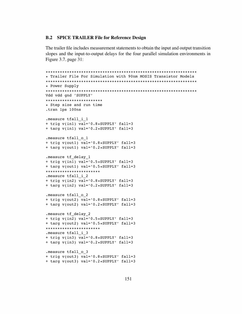
B.2 SPICE TRAILER File for Reference Design
The trailer file includes measurement statements to obtain the input and output transitionslopes and the input-to-output delays for the four parallel simulation environments inFigure 3.7, page 31:
***************************************************************** Trailer File For Simulation with 90nm MOSIS Transistor Models***************************************************************** Power Supply
****************************************************************Vdd vdd gnd ’SUPPLY’
************************* Step size and run time.tran 1ps 100ns
.measure tfall_i_1+ trig v(in1) val=’0.8*SUPPLY’ fall=3+ targ v(in1) val=’0.2*SUPPLY’ fall=3
.measure tfall_o_1+ trig v(out1) val=’0.8*SUPPLY’ fall=3+ targ v(out1) val=’0.2*SUPPLY’ fall=3
.measure tf_delay_1+ trig v(in1) val=’0.5*SUPPLY’ fall=3+ targ v(out1) val=’0.5*SUPPLY’ fall=3***********************.measure tfall_i_2+ trig v(in2) val=’0.8*SUPPLY’ fall=3+ targ v(in2) val=’0.2*SUPPLY’ fall=3
.measure tfall_o_2+ trig v(out2) val=’0.8*SUPPLY’ fall=3+ targ v(out2) val=’0.2*SUPPLY’ fall=3
.measure tf_delay_2+ trig v(in2) val=’0.5*SUPPLY’ fall=3+ targ v(out2) val=’0.5*SUPPLY’ fall=3
***********************.measure tfall_i_3+ trig v(in3) val=’0.8*SUPPLY’ fall=3+ targ v(in3) val=’0.2*SUPPLY’ fall=3
.measure tfall_o_3+ trig v(out3) val=’0.8*SUPPLY’ fall=3+ targ v(out3) val=’0.2*SUPPLY’ fall=3
151
.measure tf_delay_3+ trig v(in3) val=’0.5*SUPPLY’ fall=3+ targ v(out3) val=’0.5*SUPPLY’ fall=3
***********************.measure tfall_i_4+ trig v(in4) val=’0.8*SUPPLY’ fall=3+ targ v(in4) val=’0.2*SUPPLY’ fall=3
.measure tfall_o_4+ trig v(out4) val=’0.8*SUPPLY’ fall=3+ targ v(out4) val=’0.2*SUPPLY’ fall=3
.measure tf_delay_4+ trig v(in4) val=’0.5*SUPPLY’ fall=3+ targ v(out4) val=’0.5*SUPPLY’ fall=3
***********************
152

B.3 SPICE Output File for Reference Design
Here are the results of the reference design experiment in Figure 3.7, page 31, withthe slope and delay times for a falling input-to-output transition in each of the foursimulation environments:
$DATA1 SOURCE=’HSPICE’ VERSION=’C-2009.03 64-BIT’.TITLE ’ ***spice deck lut_b1_validate{sch}, library lut_parta’tfall_i_1 tfall_o_1 tf_delay_1 tfall_i_2tfall_o_2 tf_delay_2 tfall_i_3 tfall_o_3tf_delay_3 tfall_i_4 tfall_o_4 tf_delay_4temper alter#1.382e-11 6.864e-12 4.793e-11 1.382e-111.229e-11 5.217e-11 1.247e-11 1.976e-115.680e-11 1.110e-11 2.411e-11 5.866e-1125.0000 1.0000
**************************************
153
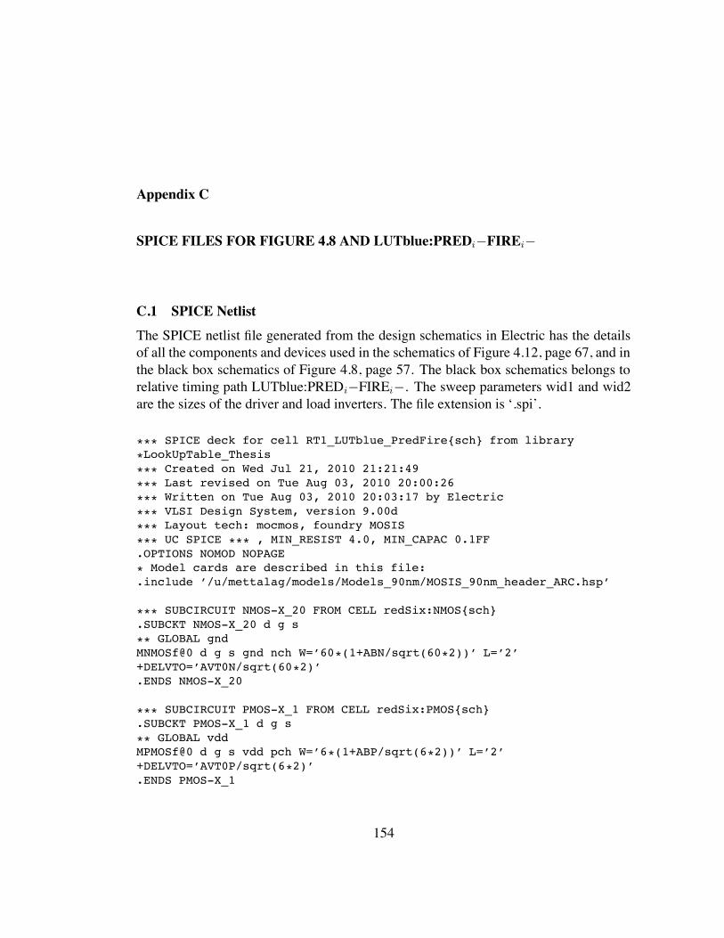
Appendix C
SPICE FILES FOR FIGURE 4.8 AND LUTblue:PREDi"FIREi"
C.1 SPICE NetlistThe SPICE netlist file generated from the design schematics in Electric has the detailsof all the components and devices used in the schematics of Figure 4.12, page 67, and inthe black box schematics of Figure 4.8, page 57. The black box schematics belongs torelative timing path LUTblue:PREDi"FIREi". The sweep parameters wid1 and wid2are the sizes of the driver and load inverters. The file extension is ‘.spi’.
*** SPICE deck for cell RT1_LUTblue_PredFire{sch} from library*LookUpTable_Thesis
*** Created on Wed Jul 21, 2010 21:21:49
*** Last revised on Tue Aug 03, 2010 20:00:26*** Written on Tue Aug 03, 2010 20:03:17 by Electric
*** VLSI Design System, version 9.00d*** Layout tech: mocmos, foundry MOSIS
*** UC SPICE *** , MIN_RESIST 4.0, MIN_CAPAC 0.1FF.OPTIONS NOMOD NOPAGE* Model cards are described in this file:.include ’/u/mettalag/models/Models_90nm/MOSIS_90nm_header_ARC.hsp’
*** SUBCIRCUIT NMOS-X_20 FROM CELL redSix:NMOS{sch}.SUBCKT NMOS-X_20 d g s** GLOBAL gndMNMOSf@0 d g s gnd nch W=’60*(1+ABN/sqrt(60*2))’ L=’2’+DELVTO=’AVT0N/sqrt(60*2)’.ENDS NMOS-X_20
*** SUBCIRCUIT PMOS-X_1 FROM CELL redSix:PMOS{sch}.SUBCKT PMOS-X_1 d g s
** GLOBAL vddMPMOSf@0 d g s vdd pch W=’6*(1+ABP/sqrt(6*2))’ L=’2’+DELVTO=’AVT0P/sqrt(6*2)’.ENDS PMOS-X_1
154

*** SUBCIRCUIT NMOS-X_30 FROM CELL redSix:NMOS{sch}.SUBCKT NMOS-X_30 d g s
** GLOBAL gndMNMOSf@0 d g s gnd nch W=’90*(1+ABN/sqrt(90*2))’ L=’2’+DELVTO=’AVT0N/sqrt(90*2)’.ENDS NMOS-X_30
*** SUBCIRCUIT PMOS-X_30 FROM CELL redSix:PMOS{sch}.SUBCKT PMOS-X_30 d g s** GLOBAL vddMPMOSf@0 d g s vdd pch W=’180*(1+ABP/sqrt(180*2))’ L=’2’+DELVTO=’AVT0P/sqrt(180*2)’.ENDS PMOS-X_30
*** SUBCIRCUIT inv-X_30 FROM CELL redSix:inv{sch}.SUBCKT inv-X_30 in out
** GLOBAL gnd** GLOBAL vddXNMOS@0 out in gnd NMOS-X_30XPMOS@0 out in vdd PMOS-X_30.ENDS inv-X_30
*** SUBCIRCUIT NMOS-X_80 FROM CELL redSix:NMOS{sch}.SUBCKT NMOS-X_80 d g s
** GLOBAL gndMNMOSf@0 d g s gnd nch W=’240*(1+ABN/sqrt(240*2))’ L=’2’+DELVTO=’AVT0N/sqrt(240*2)’.ENDS NMOS-X_80
*** SUBCIRCUIT PMOS-X_80 FROM CELL redSix:PMOS{sch}.SUBCKT PMOS-X_80 d g s
** GLOBAL vddMPMOSf@0 d g s vdd pch W=’480*(1+ABP/sqrt(480*2))’ L=’2’+DELVTO=’AVT0P/sqrt(480*2)’.ENDS PMOS-X_80
*** SUBCIRCUIT inv-X_80 FROM CELL redSix:inv{sch}.SUBCKT inv-X_80 in out** GLOBAL gnd
** GLOBAL vddXNMOS@0 out in gnd NMOS-X_80XPMOS@0 out in vdd PMOS-X_80.ENDS inv-X_80
*** SUBCIRCUIT NMOS-X_5 FROM CELL redSix:NMOS{sch}.SUBCKT NMOS-X_5 d g s** GLOBAL gndMNMOSf@0 d g s gnd nch W=’15*(1+ABN/sqrt(15*2))’ L=’2’+DELVTO=’AVT0N/sqrt(15*2)’
155
.ENDS NMOS-X_5
*** SUBCIRCUIT PMOS-X_5 FROM CELL redSix:PMOS{sch}.SUBCKT PMOS-X_5 d g s** GLOBAL vddMPMOSf@0 d g s vdd pch W=’30*(1+ABP/sqrt(30*2))’ L=’2’+DELVTO=’AVT0P/sqrt(30*2)’.ENDS PMOS-X_5
*** SUBCIRCUIT inv-X_5 FROM CELL redSix:inv{sch}.SUBCKT inv-X_5 in out
** GLOBAL gnd** GLOBAL vddXNMOS@0 out in gnd NMOS-X_5XPMOS@0 out in vdd PMOS-X_5.ENDS inv-X_5
*** SUBCIRCUIT NMOS-X_2 FROM CELL redSix:NMOS{sch}.SUBCKT NMOS-X_2 d g s
** GLOBAL gndMNMOSf@0 d g s gnd nch W=’6*(1+ABN/sqrt(6*2))’+ L=’2’ DELVTO=’AVT0N/sqrt(6*2)’.ENDS NMOS-X_2
*** SUBCIRCUIT PMOS-X_2 FROM CELL redSix:PMOS{sch}.SUBCKT PMOS-X_2 d g s
** GLOBAL vddMPMOSf@0 d g s vdd pch W=’12*(1+ABP/sqrt(12*2))’ L=’2’+DELVTO=’AVT0P/sqrt(12*2)’.ENDS PMOS-X_2
*** SUBCIRCUIT inv-X_2 FROM CELL redSix:inv{sch}.SUBCKT inv-X_2 in out** GLOBAL gnd
** GLOBAL vddXNMOS@0 out in gnd NMOS-X_2XPMOS@0 out in vdd PMOS-X_2.ENDS inv-X_2
*** SUBCIRCUIT NMOS-X_10 FROM CELL redSix:NMOS{sch}.SUBCKT NMOS-X_10 d g s** GLOBAL gndMNMOSf@0 d g s gnd nch W=’30*(1+ABN/sqrt(30*2))’ L=’2’+DELVTO=’AVT0N/sqrt(30*2)’.ENDS NMOS-X_10
*** SUBCIRCUIT PMOS-X_20 FROM CELL redSix:PMOS{sch}.SUBCKT PMOS-X_20 d g s
** GLOBAL vdd
156

MPMOSf@0 d g s vdd pch W=’120*(1+ABP/sqrt(120*2))’ L=’2’+DELVTO=’AVT0P/sqrt(120*2)’.ENDS PMOS-X_20
*** SUBCIRCUIT pms2-X_10 FROM CELL redSix:pms2{sch}.SUBCKT pms2-X_10 d g g2** GLOBAL vddXPMOS@0 net@2 g vdd PMOS-X_20XPMOS@1 d g2 net@2 PMOS-X_20.ENDS pms2-X_10
*** SUBCIRCUIT nor2-X_10 FROM CELL redSix:nor2{sch}.SUBCKT nor2-X_10 ina inb out
** GLOBAL gnd** GLOBAL vddXNMOS@0 out ina gnd NMOS-X_10XNMOS@1 out inb gnd NMOS-X_10Xpms2@0 out ina inb pms2-X_10.ENDS nor2-X_10
*** SUBCIRCUIT LUTblue_RT1_path FROM CELL LUTblue_RT1_path{sch}.SUBCKT LUTblue_RT1_path fire pred** GLOBAL gnd
** GLOBAL vddXNMOS@0 NMOS@0_d fire gnd NMOS-X_20XPMOS@0 net@57 net@2 vdd PMOS-X_1XPMOS@1 net@57 fire net@4 PMOS-X_1EVCVS@0 net@13 gnd vcvs net@9 gnd 1 max=’10V’ min=’-10V’Xinv@0 net@20 net@19 inv-X_30Xinv@1 net@19 fire inv-X_80Xinv@2 pred net@9 inv-X_5Xinv@4 net@4 net@2 inv-X_2Xnor2n@0 net@13 net@9 net@20 nor2-X_10
* Spice Code nodes in cell cell ’LUTblue_RT1_path{sch}’.ic succ=0v net@68=1v.ENDS LUTblue_RT1_path
*** SUBCIRCUIT NMOS-X_wid1 FROM CELL redSix:NMOS{sch}.SUBCKT NMOS-X_wid1 d g s
** GLOBAL gndMNMOSf@0 d g s gnd nch W=’3*wid1*(1+ABN/sqrt(3*wid1*2))’ L=’2’+DELVTO=’AVT0N/sqrt(3*wid1*2)’.ENDS NMOS-X_wid1
*** SUBCIRCUIT PMOS-X_wid1 FROM CELL redSix:PMOS{sch}.SUBCKT PMOS-X_wid1 d g s
** GLOBAL vddMPMOSf@0 d g s vdd pch W=’2*3*wid1*(1+ABP/sqrt(2*3*wid1*2))’
157
+ L=’2’ DELVTO=’AVT0P/sqrt(2*3*wid1*2)’.ENDS PMOS-X_wid1
*** SUBCIRCUIT inv-X_wid1 FROM CELL redSix:inv{sch}.SUBCKT inv-X_wid1 in out
** GLOBAL gnd** GLOBAL vddXNMOS@0 out in gnd NMOS-X_wid1XPMOS@0 out in vdd PMOS-X_wid1.ENDS inv-X_wid1
*** SUBCIRCUIT NMOS-X_wids FROM CELL redSix:NMOS{sch}.SUBCKT NMOS-X_wids d g s
** GLOBAL gndMNMOSf@0 d g s gnd nch W=’3*(wid1/3)*+(1+ABN/sqrt(3*(wid1/3)*2))’+ L=’2’ DELVTO=’AVT0N/sqrt(3*(wid1/3)*2)’.ENDS NMOS-X_wids
*** SUBCIRCUIT PMOS-X_wids FROM CELL redSix:PMOS{sch}.SUBCKT PMOS-X_wids d g s
** GLOBAL vddMPMOSf@0 d g s vdd pch W=’2*3*(wid1/3)*(1+ABP/sqrt(2*3*+(wid1/3)*2))’ L=’2’ DELVTO=’AVT0P/sqrt(2*3*(wid1/3)*2)’.ENDS PMOS-X_wids
*** SUBCIRCUIT inv-X_wids FROM CELL redSix:inv{sch}.SUBCKT inv-X_wids in out** GLOBAL gnd
** GLOBAL vddXNMOS@0 out in gnd NMOS-X_widsXPMOS@0 out in vdd PMOS-X_wids.ENDS inv-X_wids
*** SUBCIRCUIT NMOS-X_widM FROM CELL redSix:NMOS{sch}.SUBCKT NMOS-X_widM d g s** GLOBAL gndMNMOSf@0 d g s gnd nch W=’3*3*wid2*+ (1+ABN/sqrt(3*3*wid2*2))’+ L=’2’ DELVTO=’AVT0N/sqrt(3*3*wid2*2)’.ENDS NMOS-X_widM
*** SUBCIRCUIT PMOS-X_widM FROM CELL redSix:PMOS{sch}.SUBCKT PMOS-X_widM d g s** GLOBAL vddMPMOSf@0 d g s vdd pch W=’2*3*3*wid2*+(1+ABP/sqrt(2*3*3*wid2*2))’ L=’2’+DELVTO=’AVT0P/sqrt(2*3*3*wid2*2)’.ENDS PMOS-X_widM
158
*** SUBCIRCUIT inv-X_widM FROM CELL redSix:inv{sch}.SUBCKT inv-X_widM in out
** GLOBAL gnd** GLOBAL vddXNMOS@0 out in gnd NMOS-X_widMXPMOS@0 out in vdd PMOS-X_widM.ENDS inv-X_widM
*** SUBCIRCUIT NMOS-X_wid2 FROM CELL redSix:NMOS{sch}.SUBCKT NMOS-X_wid2 d g s
** GLOBAL gndMNMOSf@0 d g s gnd nch W=’3*wid2*+(1+ABN/sqrt(3*wid2*2))’ L=’2’+DELVTO=’AVT0N/sqrt(3*wid2*2)’.ENDS NMOS-X_wid2
*** SUBCIRCUIT PMOS-X_wid2 FROM CELL redSix:PMOS{sch}.SUBCKT PMOS-X_wid2 d g s
** GLOBAL vddMPMOSf@0 d g s vdd pch W=’2*3*wid2*+(1+ABP/sqrt(2*3*wid2*2))’ L=’2’+DELVTO=’AVT0P/sqrt(2*3*wid2*2)’.ENDS PMOS-X_wid2
*** SUBCIRCUIT inv-X_wid2 FROM CELL redSix:inv{sch}.SUBCKT inv-X_wid2 in out
** GLOBAL gnd** GLOBAL vddXNMOS@0 out in gnd NMOS-X_wid2XPMOS@0 out in vdd PMOS-X_wid2.ENDS inv-X_wid2
.global gnd vdd
*** TOP LEVEL CELL: RT1_LUTblue_PredFire{sch}XLUTblue_@0 out[1] in[1] LUTblue_RT1_pathVPulse@0 net@67 gnd pulse 0 ’1v’ ’0ns’ ’50ps’ ’50ps’ ’2ns’ ’4ns’Xinv@1 Din[1] in[1] inv-X_wid1Xinv@2 net@67 Din[1] inv-X_widsXinv@3 net@64 inv@3_out inv-X_widMXinv@4 out[1] net@64 inv-X_wid2
* Trailer cards are described in this file:.include ’/u/mettalag/models/Models_90nm/MOSIS_trailer_ARC_1.hsp’.END
159

C.2 SPICE Simulation Setup File: HEADERHere is the basic file with default simulation parameters for SPICE. Its extension is‘.hsp’. It contains a pointer to the 90nm CMOS process models for our GasP designs.We use the library with typical (TT) Process, Voltage and Temperature (PVT) settings.
***************************************************************** Header File for Simulation with 90nm MOSIS Transistor Models*****************************************************************
********************************************************************************************************************************.LIB ’/stash/arc/models/tsmc90/hspice/cmn90g_2d5_lk_v1d0.l’ TT
*.LIB ’/stash/arc/models/tsmc90/hspice/cmn90g_1d8_3d3_lk_v1d0.l’ TT
***************************************************************** Options and Parameters****************************************************************.OPTION nomod POST.OPTION SCALE=50n.OPTION CAPTAB.PARAM hdifp=0.PARAM hdifn=0.PARAM ABN=0.PARAM ABP=0.PARAM AVT0P=0.PARAM AVT0N=0.PARAM SUPPLY=1V
***************************************************************** Netlist****************************************************************
160
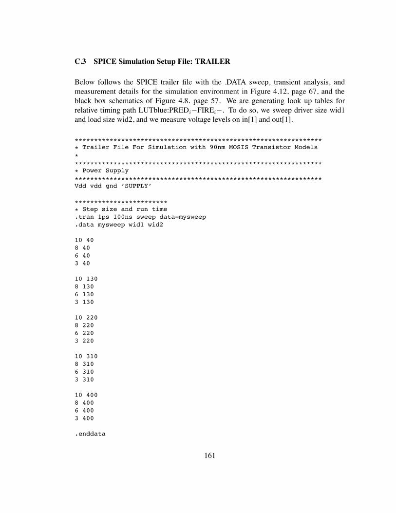
C.3 SPICE Simulation Setup File: TRAILER
Below follows the SPICE trailer file with the .DATA sweep, transient analysis, andmeasurement details for the simulation environment in Figure 4.12, page 67, and theblack box schematics of Figure 4.8, page 57. We are generating look up tables forrelative timing path LUTblue:PREDi"FIREi". To do so, we sweep driver size wid1and load size wid2, and we measure voltage levels on in[1] and out[1].
***************************************************************** Trailer File For Simulation with 90nm MOSIS Transistor Models****************************************************************** Power Supply****************************************************************Vdd vdd gnd ’SUPPLY’
************************* Step size and run time.tran 1ps 100ns sweep data=mysweep.data mysweep wid1 wid2
10 408 406 403 40
10 1308 1306 1303 130
10 2208 2206 2203 220
10 3108 3106 3103 310
10 4008 4006 4003 400
.enddata
161

.measure tfall_i_1+ trig v(in[1]) val=’0.8*SUPPLY’ fall=3+ targ v(in[1]) val=’0.2*SUPPLY’ fall=3
.measure tfall_o_1+ trig v(out[1]) val=’0.8*SUPPLY’ fall=3+ targ v(out[1]) val=’0.2*SUPPLY’ fall=3
.measure tf_delay+ trig v(in[1]) val=’0.5*SUPPLY’ fall=3+ targ v(out[1]) val=’0.5*SUPPLY’ fall=3
***********************
162
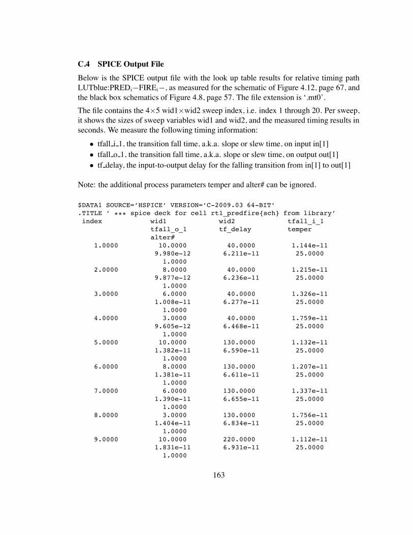
C.4 SPICE Output FileBelow is the SPICE output file with the look up table results for relative timing pathLUTblue:PREDi"FIREi", as measured for the schematic of Figure 4.12, page 67, andthe black box schematics of Figure 4.8, page 57. The file extension is ‘.mt0’.The file contains the 4#5 wid1#wid2 sweep index, i.e. index 1 through 20. Per sweep,it shows the sizes of sweep variables wid1 and wid2, and the measured timing results inseconds. We measure the following timing information:
• tfall i 1, the transition fall time, a.k.a. slope or slew time, on input in[1]• tfall o 1, the transition fall time, a.k.a. slope or slew time, on output out[1]• tf delay, the input-to-output delay for the falling transition from in[1] to out[1]
Note: the additional process parameters temper and alter# can be ignored.
$DATA1 SOURCE=’HSPICE’ VERSION=’C-2009.03 64-BIT’.TITLE ’ *** spice deck for cell rt1_predfire{sch} from library’index wid1 wid2 tfall_i_1
tfall_o_1 tf_delay temperalter#
1.0000 10.0000 40.0000 1.144e-119.980e-12 6.211e-11 25.0000
1.00002.0000 8.0000 40.0000 1.215e-11
9.877e-12 6.236e-11 25.00001.0000
3.0000 6.0000 40.0000 1.326e-111.008e-11 6.277e-11 25.0000
1.00004.0000 3.0000 40.0000 1.759e-11
9.605e-12 6.468e-11 25.00001.0000
5.0000 10.0000 130.0000 1.132e-111.382e-11 6.590e-11 25.0000
1.00006.0000 8.0000 130.0000 1.207e-11
1.381e-11 6.611e-11 25.00001.0000
7.0000 6.0000 130.0000 1.337e-111.390e-11 6.655e-11 25.0000
1.00008.0000 3.0000 130.0000 1.756e-11
1.404e-11 6.834e-11 25.00001.0000
9.0000 10.0000 220.0000 1.112e-111.831e-11 6.931e-11 25.0000
1.0000
163
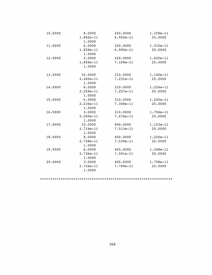
10.0000 8.0000 220.0000 1.159e-111.842e-11 6.954e-11 25.0000
1.000011.0000 6.0000 220.0000 1.315e-11
1.838e-11 6.990e-11 25.00001.0000
12.0000 3.0000 220.0000 1.625e-111.856e-11 7.169e-11 25.0000
1.0000
13.0000 10.0000 310.0000 1.140e-112.265e-11 7.231e-11 25.0000
1.000014.0000 8.0000 310.0000 1.224e-11
2.259e-11 7.257e-11 25.00001.0000
15.0000 6.0000 310.0000 1.245e-112.234e-11 7.308e-11 25.0000
1.000016.0000 3.0000 310.0000 1.756e-11
2.200e-11 7.476e-11 25.00001.0000
17.0000 10.0000 400.0000 1.153e-112.714e-11 7.513e-11 25.0000
1.000018.0000 8.0000 400.0000 1.220e-11
2.728e-11 7.539e-11 25.00001.0000
19.0000 6.0000 400.0000 1.308e-112.736e-11 7.591e-11 25.0000
1.000020.0000 3.0000 400.0000 1.758e-11
2.734e-11 7.769e-11 25.00001.0000
****************************************************************
164
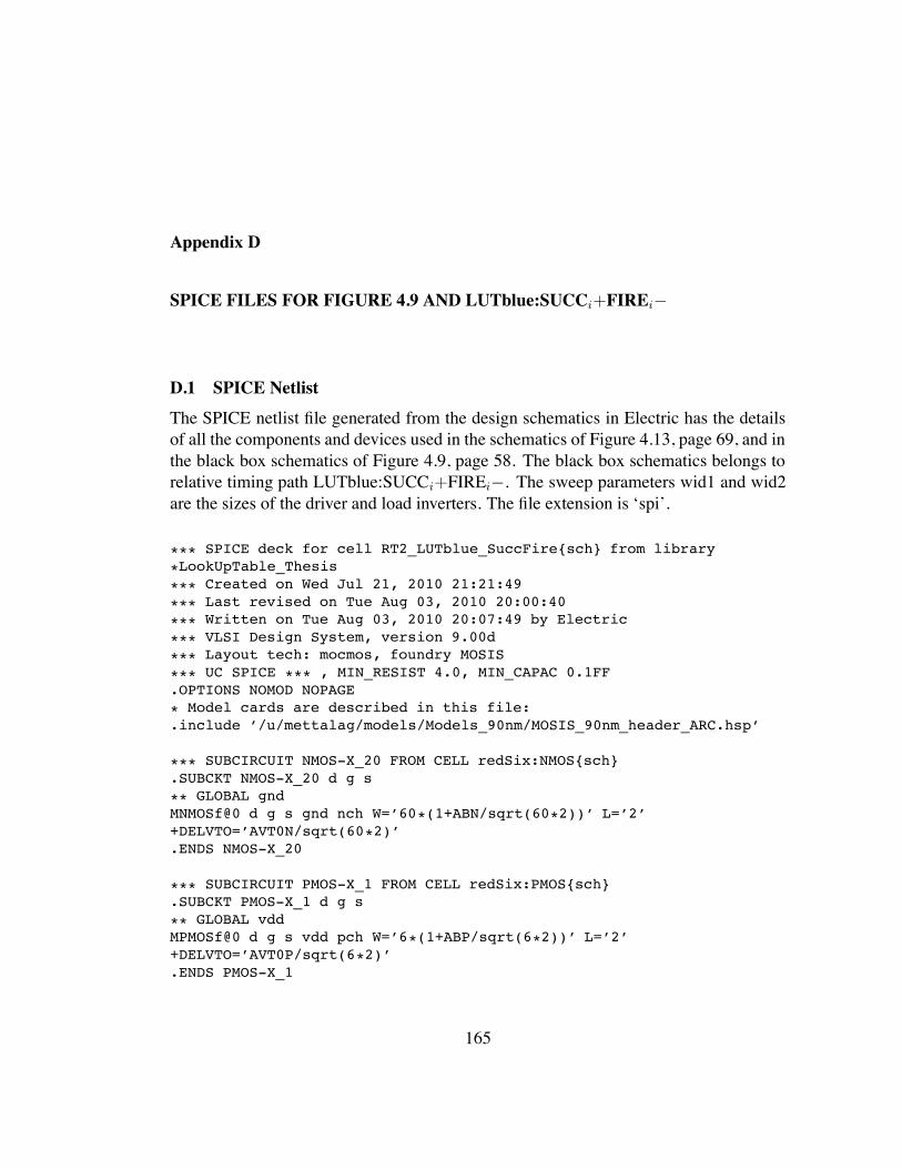
Appendix D
SPICE FILES FOR FIGURE 4.9 AND LUTblue:SUCCi+FIREi"
D.1 SPICE NetlistThe SPICE netlist file generated from the design schematics in Electric has the detailsof all the components and devices used in the schematics of Figure 4.13, page 69, and inthe black box schematics of Figure 4.9, page 58. The black box schematics belongs torelative timing path LUTblue:SUCCi+FIREi". The sweep parameters wid1 and wid2are the sizes of the driver and load inverters. The file extension is ‘spi’.
*** SPICE deck for cell RT2_LUTblue_SuccFire{sch} from library*LookUpTable_Thesis
*** Created on Wed Jul 21, 2010 21:21:49
*** Last revised on Tue Aug 03, 2010 20:00:40*** Written on Tue Aug 03, 2010 20:07:49 by Electric
*** VLSI Design System, version 9.00d*** Layout tech: mocmos, foundry MOSIS
*** UC SPICE *** , MIN_RESIST 4.0, MIN_CAPAC 0.1FF.OPTIONS NOMOD NOPAGE* Model cards are described in this file:.include ’/u/mettalag/models/Models_90nm/MOSIS_90nm_header_ARC.hsp’
*** SUBCIRCUIT NMOS-X_20 FROM CELL redSix:NMOS{sch}.SUBCKT NMOS-X_20 d g s** GLOBAL gndMNMOSf@0 d g s gnd nch W=’60*(1+ABN/sqrt(60*2))’ L=’2’+DELVTO=’AVT0N/sqrt(60*2)’.ENDS NMOS-X_20
*** SUBCIRCUIT PMOS-X_1 FROM CELL redSix:PMOS{sch}.SUBCKT PMOS-X_1 d g s
** GLOBAL vddMPMOSf@0 d g s vdd pch W=’6*(1+ABP/sqrt(6*2))’ L=’2’+DELVTO=’AVT0P/sqrt(6*2)’.ENDS PMOS-X_1
165
*** SUBCIRCUIT NMOS-X_30 FROM CELL redSix:NMOS{sch}.SUBCKT NMOS-X_30 d g s
** GLOBAL gndMNMOSf@0 d g s gnd nch W=’90*(1+ABN/sqrt(90*2))’ L=’2’+DELVTO=’AVT0N/sqrt(90*2)’.ENDS NMOS-X_30
*** SUBCIRCUIT PMOS-X_30 FROM CELL redSix:PMOS{sch}.SUBCKT PMOS-X_30 d g s** GLOBAL vddMPMOSf@0 d g s vdd pch W=’180*(1+ABP/sqrt(180*2))’ L=’2’+DELVTO=’AVT0P/sqrt(180*2)’.ENDS PMOS-X_30
*** SUBCIRCUIT inv-X_30 FROM CELL redSix:inv{sch}.SUBCKT inv-X_30 in out
** GLOBAL gnd** GLOBAL vddXNMOS@0 out in gnd NMOS-X_30XPMOS@0 out in vdd PMOS-X_30.ENDS inv-X_30
*** SUBCIRCUIT NMOS-X_80 FROM CELL redSix:NMOS{sch}.SUBCKT NMOS-X_80 d g s
** GLOBAL gndMNMOSf@0 d g s gnd nch W=’240*(1+ABN/sqrt(240*2))’ L=’2’+DELVTO=’AVT0N/sqrt(240*2)’.ENDS NMOS-X_80
*** SUBCIRCUIT PMOS-X_80 FROM CELL redSix:PMOS{sch}.SUBCKT PMOS-X_80 d g s
** GLOBAL vddMPMOSf@0 d g s vdd pch W=’480*(1+ABP/sqrt(480*2))’ L=’2’+DELVTO=’AVT0P/sqrt(480*2)’.ENDS PMOS-X_80
*** SUBCIRCUIT inv-X_80 FROM CELL redSix:inv{sch}.SUBCKT inv-X_80 in out** GLOBAL gnd
** GLOBAL vddXNMOS@0 out in gnd NMOS-X_80XPMOS@0 out in vdd PMOS-X_80.ENDS inv-X_80
*** SUBCIRCUIT NMOS-X_5 FROM CELL redSix:NMOS{sch}.SUBCKT NMOS-X_5 d g s** GLOBAL gndMNMOSf@0 d g s gnd nch W=’15*(1+ABN/sqrt(15*2))’L=’2’+DELVTO=’AVT0N/sqrt(15*2)’
166
.ENDS NMOS-X_5
*** SUBCIRCUIT PMOS-X_5 FROM CELL redSix:PMOS{sch}.SUBCKT PMOS-X_5 d g s** GLOBAL vddMPMOSf@0 d g s vdd pch W=’30*(1+ABP/sqrt(30*2))’L=’2’+DELVTO=’AVT0P/sqrt(30*2)’.ENDS PMOS-X_5
*** SUBCIRCUIT inv-X_5 FROM CELL redSix:inv{sch}.SUBCKT inv-X_5 in out
** GLOBAL gnd** GLOBAL vddXNMOS@0 out in gnd NMOS-X_5XPMOS@0 out in vdd PMOS-X_5.ENDS inv-X_5
*** SUBCIRCUIT NMOS-X_2 FROM CELL redSix:NMOS{sch}.SUBCKT NMOS-X_2 d g s
** GLOBAL gndMNMOSf@0 d g s gnd nch W=’6*(1+ABN/sqrt(6*2))’+ L=’2’ DELVTO=’AVT0N/sqrt(6*2)’.ENDS NMOS-X_2
*** SUBCIRCUIT PMOS-X_2 FROM CELL redSix:PMOS{sch}.SUBCKT PMOS-X_2 d g s
** GLOBAL vddMPMOSf@0 d g s vdd pch W=’12*(1+ABP/sqrt(12*2))’ L=’2’+DELVTO=’AVT0P/sqrt(12*2)’.ENDS PMOS-X_2
*** SUBCIRCUIT inv-X_2 FROM CELL redSix:inv{sch}.SUBCKT inv-X_2 in out** GLOBAL gnd
** GLOBAL vddXNMOS@0 out in gnd NMOS-X_2XPMOS@0 out in vdd PMOS-X_2.ENDS inv-X_2
*** SUBCIRCUIT NMOS-X_10 FROM CELL redSix:NMOS{sch}.SUBCKT NMOS-X_10 d g s** GLOBAL gndMNMOSf@0 d g s gnd nch W=’30*(1+ABN/sqrt(30*2))’ L=’2’+DELVTO=’AVT0N/sqrt(30*2)’.ENDS NMOS-X_10
*** SUBCIRCUIT PMOS-X_20 FROM CELL redSix:PMOS{sch}.SUBCKT PMOS-X_20 d g s
** GLOBAL vdd
167
MPMOSf@0 d g s vdd pch W=’120*(1+ABP/sqrt(120*2))’ L=’2’+DELVTO=’AVT0P/sqrt(120*2)’.ENDS PMOS-X_20
*** SUBCIRCUIT pms2-X_10 FROM CELL redSix:pms2{sch}.SUBCKT pms2-X_10 d g g2** GLOBAL vddXPMOS@0 net@2 g vdd PMOS-X_20XPMOS@1 d g2 net@2 PMOS-X_20.ENDS pms2-X_10
*** SUBCIRCUIT nor2-X_10 FROM CELL redSix:nor2{sch}.SUBCKT nor2-X_10 ina inb out
** GLOBAL gnd** GLOBAL vddXNMOS@0 out ina gnd NMOS-X_10XNMOS@1 out inb gnd NMOS-X_10Xpms2@0 out ina inb pms2-X_10.ENDS nor2-X_10
*** SUBCIRCUIT LUTblue_RT2_path FROM CELL LUTblue_RT2_path{sch}.SUBCKT LUTblue_RT2_path fire succ** GLOBAL gnd
** GLOBAL vddXNMOS@0 NMOS@0_d fire gnd NMOS-X_20XPMOS@0 net@57 net@2 vdd PMOS-X_1XPMOS@1 net@57 fire net@4 PMOS-X_1EVCVS@0 net@9 gnd vcvs succ gnd 1 max=’10V’ min=’-10V’Xinv@0 net@20 net@19 inv-X_30Xinv@1 net@19 fire inv-X_80Xinv@2 inv@2_in net@9 inv-X_5Xinv@4 net@4 net@2 inv-X_2Xnor2n@0 succ net@9 net@20 nor2-X_10
* Spice Code nodes in cell cell ’LUTblue_RT2_path{sch}’.ic succ=0v net@85=1v.ENDS LUTblue_RT2_path
*** SUBCIRCUIT NMOS-X_wid1 FROM CELL redSix:NMOS{sch}.SUBCKT NMOS-X_wid1 d g s
** GLOBAL gndMNMOSf@0 d g s gnd nch W=’3*wid1*(1+ABN/sqrt(3*wid1*2))’ L=’2’+DELVTO=’AVT0N/sqrt(3*wid1*2)’.ENDS NMOS-X_wid1
*** SUBCIRCUIT PMOS-X_wid1 FROM CELL redSix:PMOS{sch}.SUBCKT PMOS-X_wid1 d g s
** GLOBAL vddMPMOSf@0 d g s vdd pch W=’2*3*wid1*(1+ABP/sqrt(2*3*wid1*2))’
168
+ L=’2’ DELVTO=’AVT0P/sqrt(2*3*wid1*2)’.ENDS PMOS-X_wid1
*** SUBCIRCUIT inv-X_wid1 FROM CELL redSix:inv{sch}.SUBCKT inv-X_wid1 in out
** GLOBAL gnd** GLOBAL vddXNMOS@0 out in gnd NMOS-X_wid1XPMOS@0 out in vdd PMOS-X_wid1.ENDS inv-X_wid1
*** SUBCIRCUIT NMOS-X_wids FROM CELL redSix:NMOS{sch}.SUBCKT NMOS-X_wids d g s
** GLOBAL gndMNMOSf@0 d g s gnd nch W=’3*(wid1/3)*(1+ABN/sqrt(3*(wid1/3)*2))’+ L=’2’ DELVTO=’AVT0N/sqrt(3*(wid1/3)*2)’.ENDS NMOS-X_wids
*** SUBCIRCUIT PMOS-X_wids FROM CELL redSix:PMOS{sch}.SUBCKT PMOS-X_wids d g s** GLOBAL vddMPMOSf@0 d g s vdd pch W=’2*3*(wid1/3)*+(1+ABP/sqrt(2*3*(wid1/3)*2))’ L=’2’+DELVTO=’AVT0P/sqrt(2*3*(wid1/3)*2)’.ENDS PMOS-X_wids
*** SUBCIRCUIT inv-X_wids FROM CELL redSix:inv{sch}.SUBCKT inv-X_wids in out** GLOBAL gnd
** GLOBAL vddXNMOS@0 out in gnd NMOS-X_widsXPMOS@0 out in vdd PMOS-X_wids.ENDS inv-X_wids
*** SUBCIRCUIT NMOS-X_widM FROM CELL redSix:NMOS{sch}.SUBCKT NMOS-X_widM d g s** GLOBAL gndMNMOSf@0 d g s gnd nch W=’3*3*wid2*(1+ABN/sqrt(3*3*wid2*2))’+ L=’2’ DELVTO=’AVT0N/sqrt(3*3*wid2*2)’.ENDS NMOS-X_widM
*** SUBCIRCUIT PMOS-X_widM FROM CELL redSix:PMOS{sch}.SUBCKT PMOS-X_widM d g s
** GLOBAL vddMPMOSf@0 d g s vdd pch W=’2*3*3*wid2*+(1+ABP/sqrt(2*3*3*wid2*2))’ L=’2’+DELVTO=’AVT0P/sqrt(2*3*3*wid2*2)’.ENDS PMOS-X_widM
169
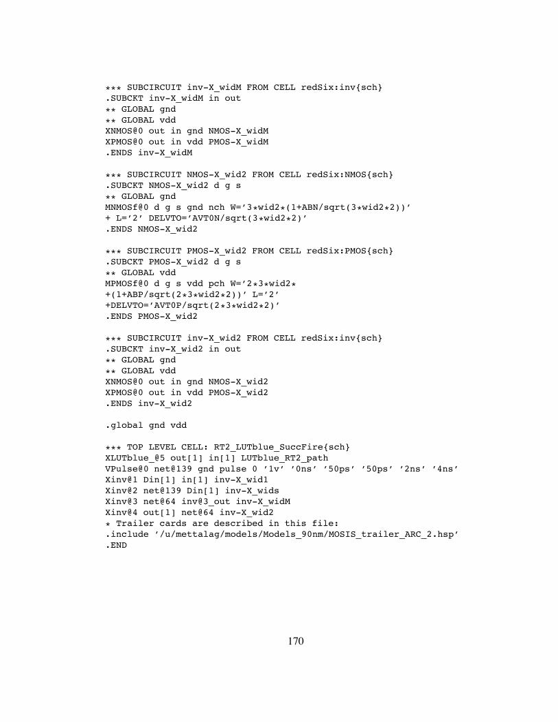
*** SUBCIRCUIT inv-X_widM FROM CELL redSix:inv{sch}.SUBCKT inv-X_widM in out
** GLOBAL gnd
** GLOBAL vddXNMOS@0 out in gnd NMOS-X_widMXPMOS@0 out in vdd PMOS-X_widM.ENDS inv-X_widM
*** SUBCIRCUIT NMOS-X_wid2 FROM CELL redSix:NMOS{sch}.SUBCKT NMOS-X_wid2 d g s
** GLOBAL gndMNMOSf@0 d g s gnd nch W=’3*wid2*(1+ABN/sqrt(3*wid2*2))’+ L=’2’ DELVTO=’AVT0N/sqrt(3*wid2*2)’.ENDS NMOS-X_wid2
*** SUBCIRCUIT PMOS-X_wid2 FROM CELL redSix:PMOS{sch}.SUBCKT PMOS-X_wid2 d g s** GLOBAL vddMPMOSf@0 d g s vdd pch W=’2*3*wid2*+(1+ABP/sqrt(2*3*wid2*2))’ L=’2’+DELVTO=’AVT0P/sqrt(2*3*wid2*2)’.ENDS PMOS-X_wid2
*** SUBCIRCUIT inv-X_wid2 FROM CELL redSix:inv{sch}.SUBCKT inv-X_wid2 in out** GLOBAL gnd
** GLOBAL vddXNMOS@0 out in gnd NMOS-X_wid2XPMOS@0 out in vdd PMOS-X_wid2.ENDS inv-X_wid2
.global gnd vdd
*** TOP LEVEL CELL: RT2_LUTblue_SuccFire{sch}XLUTblue_@5 out[1] in[1] LUTblue_RT2_pathVPulse@0 net@139 gnd pulse 0 ’1v’ ’0ns’ ’50ps’ ’50ps’ ’2ns’ ’4ns’Xinv@1 Din[1] in[1] inv-X_wid1Xinv@2 net@139 Din[1] inv-X_widsXinv@3 net@64 inv@3_out inv-X_widMXinv@4 out[1] net@64 inv-X_wid2
* Trailer cards are described in this file:.include ’/u/mettalag/models/Models_90nm/MOSIS_trailer_ARC_2.hsp’.END
170
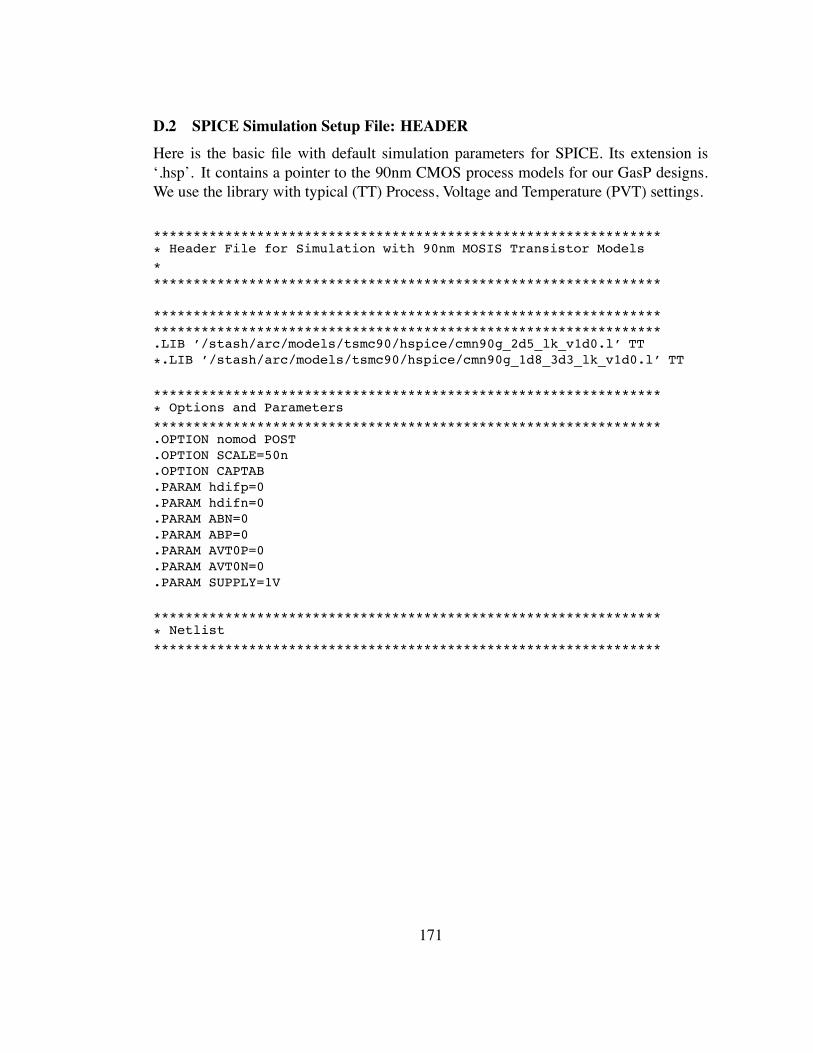
D.2 SPICE Simulation Setup File: HEADERHere is the basic file with default simulation parameters for SPICE. Its extension is‘.hsp’. It contains a pointer to the 90nm CMOS process models for our GasP designs.We use the library with typical (TT) Process, Voltage and Temperature (PVT) settings.
***************************************************************** Header File for Simulation with 90nm MOSIS Transistor Models*****************************************************************
********************************************************************************************************************************.LIB ’/stash/arc/models/tsmc90/hspice/cmn90g_2d5_lk_v1d0.l’ TT
*.LIB ’/stash/arc/models/tsmc90/hspice/cmn90g_1d8_3d3_lk_v1d0.l’ TT
***************************************************************** Options and Parameters****************************************************************.OPTION nomod POST.OPTION SCALE=50n.OPTION CAPTAB.PARAM hdifp=0.PARAM hdifn=0.PARAM ABN=0.PARAM ABP=0.PARAM AVT0P=0.PARAM AVT0N=0.PARAM SUPPLY=1V
***************************************************************** Netlist****************************************************************
171
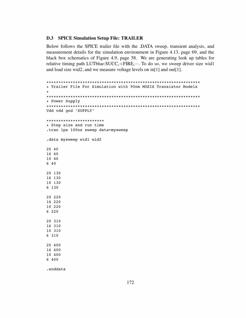
D.3 SPICE Simulation Setup File: TRAILERBelow follows the SPICE trailer file with the .DATA sweep, transient analysis, andmeasurement details for the simulation environment in Figure 4.13, page 69, and theblack box schematics of Figure 4.9, page 58. We are generating look up tables forrelative timing path LUTblue:SUCCi+FIREi". To do so, we sweep driver size wid1and load size wid2, and we measure voltage levels on in[1] and out[1].
***************************************************************** Trailer File For Simulation with 90nm MOSIS Transistor Models
****************************************************************** Power Supply
****************************************************************Vdd vdd gnd ’SUPPLY’
************************* Step size and run time.tran 1ps 100ns sweep data=mysweep
.data mysweep wid1 wid2
20 4016 4010 406 40
20 13016 13010 1306 130
20 22016 22010 2206 220
20 31016 31010 3106 310
20 40016 40010 4006 400
.enddata
172

.measure trise_i_1+ trig v(in[1]) val=’0.2*SUPPLY’ rise=3+ targ v(in[1]) val=’0.8*SUPPLY’ rise=3
.measure tfall_o_1+ trig v(out[1]) val=’0.8*SUPPLY’ fall=3+ targ v(out[1]) val=’0.2*SUPPLY’ fall=3
.measure TpHL_1+ trig v(in[1]) val=’0.5*SUPPLY’ rise=3+ targ v(out[1]) val=’0.5*SUPPLY’ fall=3
***********************
173
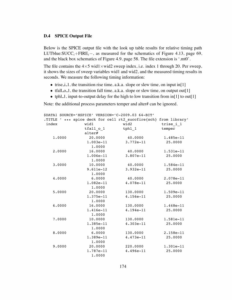
D.4 SPICE Output File
Below is the SPICE output file with the look up table results for relative timing pathLUTblue:SUCCi+FIREi", as measured for the schematics of Figure 4.13, page 69,and the black box schematics of Figure 4.9, page 58. The file extension is ‘.mt0’.The file contains the 4#5 wid1#wid2 sweep index, i.e. index 1 through 20. Per sweep,it shows the sizes of sweep variables wid1 and wid2, and the measured timing results inseconds. We measure the following timing information:
• trise i 1, the transition rise time, a.k.a. slope or slew time, on input in[1]• tfall o 1, the transition fall time, a.k.a. slope or slew time, on output out[1]• tphl 1, input-to-output delay for the high to low transition from in[1] to out[1]
Note: the additional process parameters temper and alter# can be ignored.
$DATA1 SOURCE=’HSPICE’ VERSION=’C-2009.03 64-BIT’.TITLE ’ *** spice deck for cell rt2_succfire{sch} from library’index wid1 wid2 trise_i_1
tfall_o_1 tphl_1 temperalter#
1.0000 20.0000 40.0000 1.485e-111.003e-11 3.772e-11 25.0000
1.00002.0000 16.0000 40.0000 1.531e-11
1.006e-11 3.807e-11 25.00001.0000
3.0000 10.0000 40.0000 1.584e-119.611e-12 3.932e-11 25.0000
1.00004.0000 6.0000 40.0000 2.078e-11
1.082e-11 4.078e-11 25.00001.0000
5.0000 20.0000 130.0000 1.509e-111.375e-11 4.156e-11 25.0000
1.00006.0000 16.0000 130.0000 1.448e-11
1.416e-11 4.194e-11 25.00001.0000
7.0000 10.0000 130.0000 1.581e-111.385e-11 4.303e-11 25.0000
1.00008.0000 6.0000 130.0000 2.158e-11
1.389e-11 4.473e-11 25.00001.0000
9.0000 20.0000 220.0000 1.301e-111.787e-11 4.496e-11 25.0000
1.0000
174
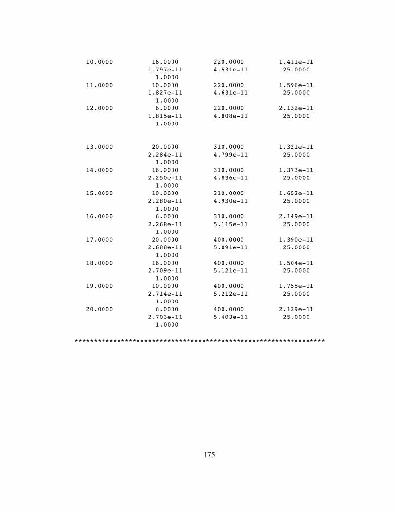
10.0000 16.0000 220.0000 1.411e-111.797e-11 4.531e-11 25.0000
1.000011.0000 10.0000 220.0000 1.596e-11
1.827e-11 4.631e-11 25.00001.0000
12.0000 6.0000 220.0000 2.132e-111.815e-11 4.808e-11 25.0000
1.0000
13.0000 20.0000 310.0000 1.321e-112.284e-11 4.799e-11 25.0000
1.000014.0000 16.0000 310.0000 1.373e-11
2.250e-11 4.836e-11 25.00001.0000
15.0000 10.0000 310.0000 1.652e-112.280e-11 4.930e-11 25.0000
1.000016.0000 6.0000 310.0000 2.149e-11
2.268e-11 5.115e-11 25.00001.0000
17.0000 20.0000 400.0000 1.390e-112.688e-11 5.091e-11 25.0000
1.000018.0000 16.0000 400.0000 1.504e-11
2.709e-11 5.121e-11 25.00001.0000
19.0000 10.0000 400.0000 1.755e-112.714e-11 5.212e-11 25.0000
1.000020.0000 6.0000 400.0000 2.129e-11
2.703e-11 5.403e-11 25.00001.0000
*****************************************************************
175
Appendix E
SPICE FILES FOR FIGURE 4.7(b) AND LUTblue:FIREi"Douti+
E.1 SPICE NetlistThe SPICE netlist file generated from the design schematics in Electric has the detailsof all the components and devices used in the schematics of Figure 4.14, page 70, and inthe black box schematics of Figure 4.7(b), page 51. The black box schematics belongsto relative timing path LUTblue:FIREi"Douti+. Sweep parameters wid1 is the size ofthe driver inverter. The file extension is ‘.spi’.
*** SPICE deck for cell RT4_LUTred_FireDout{sch} from library*LookUpTable_Thesis
*** Created on Wed Jul 21, 2010 21:21:49
*** Last revised on Tue Aug 03, 2010 20:01:01*** Written on Tue Aug 03, 2010 20:12:05 by Electric VLSI
*** Design System, version 9.00d*** Layout tech: mocmos, foundry MOSIS
*** UC SPICE *** , MIN_RESIST 4.0, MIN_CAPAC 0.1FF.OPTIONS NOMOD NOPAGE* Model cards are described in this file:.include ’/u/mettalag/models/Models_90nm/MOSIS_90nm_header_ARC.hsp’
*** SUBCIRCUIT NMOS-X_1 FROM CELL redSix:NMOS{sch}.SUBCKT NMOS-X_1 d g s** GLOBAL gndMNMOSf@0 d g s gnd nch W=’3*(1+ABN/sqrt(3*2))’+ L=’2’ DELVTO=’AVT0N/sqrt(3*2)’.ENDS NMOS-X_1
*** SUBCIRCUIT PMOS-X_20 FROM CELL redSix:PMOS{sch}.SUBCKT PMOS-X_20 d g s
** GLOBAL vddMPMOSf@0 d g s vdd pch W=’120*(1+ABP/sqrt(120*2))’ L=’2’+DELVTO=’AVT0P/sqrt(120*2)’.ENDS PMOS-X_20
176
*** SUBCIRCUIT NMOS-X_4 FROM CELL redSix:NMOS{sch}.SUBCKT NMOS-X_4 d g s
** GLOBAL gndMNMOSf@0 d g s gnd nch W=’12*(1+ABN/sqrt(12*2))’ L=’2’+DELVTO=’AVT0N/sqrt(12*2)’.ENDS NMOS-X_4
*** SUBCIRCUIT PMOS-X_4 FROM CELL redSix:PMOS{sch}.SUBCKT PMOS-X_4 d g s** GLOBAL vddMPMOSf@0 d g s vdd pch W=’24*(1+ABP/sqrt(24*2))’ L=’2’+DELVTO=’AVT0P/sqrt(24*2)’.ENDS PMOS-X_4
*** SUBCIRCUIT inv-X_4 FROM CELL redSix:inv{sch}.SUBCKT inv-X_4 in out
** GLOBAL gnd** GLOBAL vddXNMOS@0 out in gnd NMOS-X_4XPMOS@0 out in vdd PMOS-X_4.ENDS inv-X_4
*** SUBCIRCUIT NMOS-X_2 FROM CELL redSix:NMOS{sch}.SUBCKT NMOS-X_2 d g s
** GLOBAL gndMNMOSf@0 d g s gnd nch W=’6*(1+ABN/sqrt(6*2))’ L=’2’+ DELVTO=’AVT0N/sqrt(6*2)’.ENDS NMOS-X_2
*** SUBCIRCUIT PMOS-X_2 FROM CELL redSix:PMOS{sch}.SUBCKT PMOS-X_2 d g s
** GLOBAL vddMPMOSf@0 d g s vdd pch W=’12*(1+ABP/sqrt(12*2))’ L=’2’+DELVTO=’AVT0P/sqrt(12*2)’.ENDS PMOS-X_2
*** SUBCIRCUIT inv-X_2 FROM CELL redSix:inv{sch}.SUBCKT inv-X_2 in out** GLOBAL gnd
** GLOBAL vddXNMOS@0 out in gnd NMOS-X_2XPMOS@0 out in vdd PMOS-X_2.ENDS inv-X_2
*** SUBCIRCUIT NMOS-X_10 FROM CELL redSix:NMOS{sch}.SUBCKT NMOS-X_10 d g s** GLOBAL gndMNMOSf@0 d g s gnd nch W=’30*(1+ABN/sqrt(30*2))’ L=’2’+DELVTO=’AVT0N/sqrt(30*2)’
177
.ENDS NMOS-X_10
*** SUBCIRCUIT pms2-X_10 FROM CELL redSix:pms2{sch}.SUBCKT pms2-X_10 d g g2** GLOBAL vddXPMOS@0 net@2 g vdd PMOS-X_20XPMOS@1 d g2 net@2 PMOS-X_20.ENDS pms2-X_10
*** SUBCIRCUIT nor2-10 FROM CELL redSix:nor2{sch}.SUBCKT nor2-10 ina inb out
** GLOBAL gnd** GLOBAL vddXNMOS@0 out ina gnd NMOS-X_10XNMOS@1 out inb gnd NMOS-X_10Xpms2@0 out ina inb pms2-X_10.ENDS nor2-10
*** SUBCIRCUIT LUTblue_RT4_path FROM CELL LUTblue_RT4_path{sch}.SUBCKT LUTblue_RT4_path dout fire** GLOBAL gnd
** GLOBAL vddXNMOS@1 net@64 net@1 gnd NMOS-X_1XNMOS@2 net@64 dout net@3 NMOS-X_1XPMOS@2 net@3 dout vdd PMOS-X_20Xinv@0 fire dout inv-X_4Xinv@1 net@3 net@1 inv-X_2Xnor2n@0 net@3 nor2n@0_inb nor2n@0_out nor2-10.ENDS LUTblue_RT4_path
*** SUBCIRCUIT NMOS-X_wid1 FROM CELL redSix:NMOS{sch}.SUBCKT NMOS-X_wid1 d g s
** GLOBAL gndMNMOSf@0 d g s gnd nch W=’3*wid1*(1+ABN/sqrt(3*wid1*2))’+L=’2’ DELVTO=’AVT0N/sqrt(3*wid1*2)’.ENDS NMOS-X_wid1
*** SUBCIRCUIT PMOS-X_wid1 FROM CELL redSix:PMOS{sch}.SUBCKT PMOS-X_wid1 d g s
** GLOBAL vddMPMOSf@0 d g s vdd pch W=’2*3*wid1*(1+ABP/sqrt(2*3*wid1*2))’+ L=’2’ DELVTO=’AVT0P/sqrt(2*3*wid1*2)’.ENDS PMOS-X_wid1
*** SUBCIRCUIT inv-X_wid1 FROM CELL redSix:inv{sch}.SUBCKT inv-X_wid1 in out** GLOBAL gnd
** GLOBAL vddXNMOS@0 out in gnd NMOS-X_wid1
178
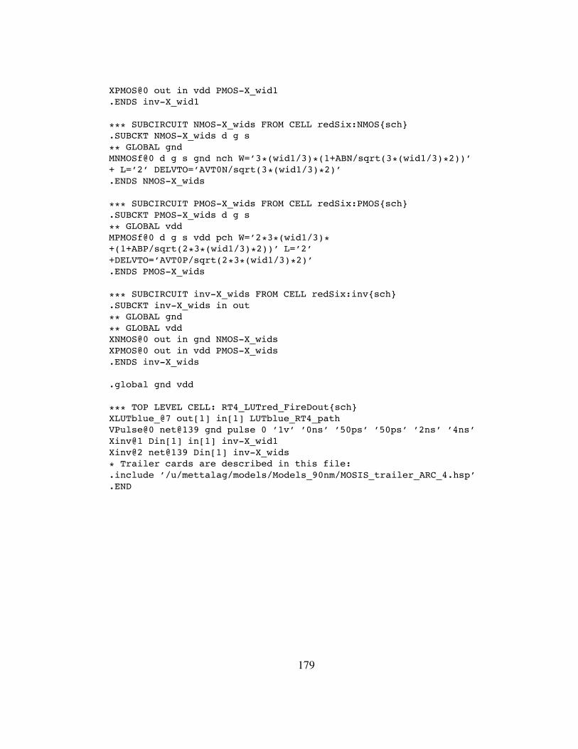
XPMOS@0 out in vdd PMOS-X_wid1.ENDS inv-X_wid1
*** SUBCIRCUIT NMOS-X_wids FROM CELL redSix:NMOS{sch}.SUBCKT NMOS-X_wids d g s
** GLOBAL gndMNMOSf@0 d g s gnd nch W=’3*(wid1/3)*(1+ABN/sqrt(3*(wid1/3)*2))’+ L=’2’ DELVTO=’AVT0N/sqrt(3*(wid1/3)*2)’.ENDS NMOS-X_wids
*** SUBCIRCUIT PMOS-X_wids FROM CELL redSix:PMOS{sch}.SUBCKT PMOS-X_wids d g s** GLOBAL vddMPMOSf@0 d g s vdd pch W=’2*3*(wid1/3)*+(1+ABP/sqrt(2*3*(wid1/3)*2))’ L=’2’+DELVTO=’AVT0P/sqrt(2*3*(wid1/3)*2)’.ENDS PMOS-X_wids
*** SUBCIRCUIT inv-X_wids FROM CELL redSix:inv{sch}.SUBCKT inv-X_wids in out** GLOBAL gnd
** GLOBAL vddXNMOS@0 out in gnd NMOS-X_widsXPMOS@0 out in vdd PMOS-X_wids.ENDS inv-X_wids
.global gnd vdd
*** TOP LEVEL CELL: RT4_LUTred_FireDout{sch}XLUTblue_@7 out[1] in[1] LUTblue_RT4_pathVPulse@0 net@139 gnd pulse 0 ’1v’ ’0ns’ ’50ps’ ’50ps’ ’2ns’ ’4ns’Xinv@1 Din[1] in[1] inv-X_wid1Xinv@2 net@139 Din[1] inv-X_wids* Trailer cards are described in this file:.include ’/u/mettalag/models/Models_90nm/MOSIS_trailer_ARC_4.hsp’.END
179

E.2 SPICE Simulation Setup File: HEADERHere is the basic file with default simulation parameters for SPICE. Its extension is‘.hsp’. It contains a pointer to the 90nm CMOS process models for our GasP designs.We use the library with typical (TT) Process, Voltage and Temperature (PVT) settings.
***************************************************************** Header File for Simulation with 90nm MOSIS Transistor Models*****************************************************************
********************************************************************************************************************************.LIB ’/stash/arc/models/tsmc90/hspice/cmn90g_2d5_lk_v1d0.l’ TT
*.LIB ’/stash/arc/models/tsmc90/hspice/cmn90g_1d8_3d3_lk_v1d0.l’ TT
***************************************************************** Options and Parameters****************************************************************.OPTION nomod POST.OPTION SCALE=50n.OPTION CAPTAB.PARAM hdifp=0.PARAM hdifn=0.PARAM ABN=0.PARAM ABP=0.PARAM AVT0P=0.PARAM AVT0N=0.PARAM SUPPLY=1V
***************************************************************** Netlist****************************************************************
180
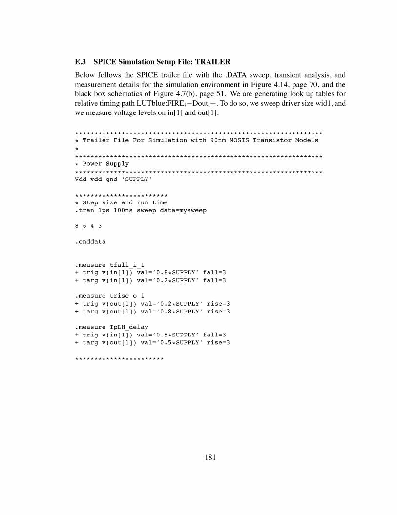
E.3 SPICE Simulation Setup File: TRAILERBelow follows the SPICE trailer file with the .DATA sweep, transient analysis, andmeasurement details for the simulation environment in Figure 4.14, page 70, and theblack box schematics of Figure 4.7(b), page 51. We are generating look up tables forrelative timing path LUTblue:FIREi"Douti+. To do so, we sweep driver size wid1, andwe measure voltage levels on in[1] and out[1].
***************************************************************** Trailer File For Simulation with 90nm MOSIS Transistor Models
****************************************************************** Power Supply
****************************************************************Vdd vdd gnd ’SUPPLY’
************************* Step size and run time.tran 1ps 100ns sweep data=mysweep
8 6 4 3
.enddata
.measure tfall_i_1+ trig v(in[1]) val=’0.8*SUPPLY’ fall=3+ targ v(in[1]) val=’0.2*SUPPLY’ fall=3
.measure trise_o_1+ trig v(out[1]) val=’0.2*SUPPLY’ rise=3+ targ v(out[1]) val=’0.8*SUPPLY’ rise=3
.measure TpLH_delay+ trig v(in[1]) val=’0.5*SUPPLY’ fall=3+ targ v(out[1]) val=’0.5*SUPPLY’ rise=3
***********************
181
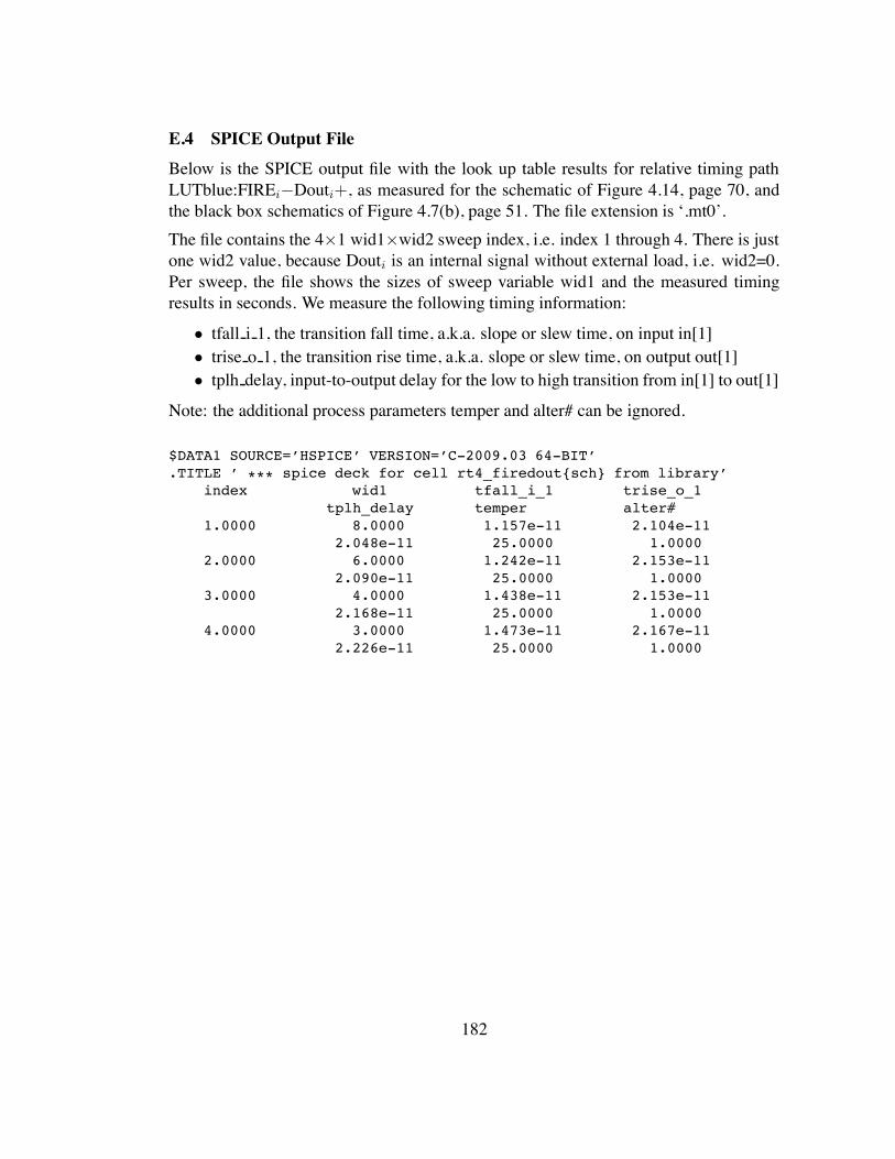
E.4 SPICE Output FileBelow is the SPICE output file with the look up table results for relative timing pathLUTblue:FIREi"Douti+, as measured for the schematic of Figure 4.14, page 70, andthe black box schematics of Figure 4.7(b), page 51. The file extension is ‘.mt0’.The file contains the 4#1 wid1#wid2 sweep index, i.e. index 1 through 4. There is justone wid2 value, because Douti is an internal signal without external load, i.e. wid2=0.Per sweep, the file shows the sizes of sweep variable wid1 and the measured timingresults in seconds. We measure the following timing information:
• tfall i 1, the transition fall time, a.k.a. slope or slew time, on input in[1]• trise o 1, the transition rise time, a.k.a. slope or slew time, on output out[1]• tplh delay, input-to-output delay for the low to high transition from in[1] to out[1]
Note: the additional process parameters temper and alter# can be ignored.
$DATA1 SOURCE=’HSPICE’ VERSION=’C-2009.03 64-BIT’.TITLE ’ *** spice deck for cell rt4_firedout{sch} from library’
index wid1 tfall_i_1 trise_o_1tplh_delay temper alter#
1.0000 8.0000 1.157e-11 2.104e-112.048e-11 25.0000 1.0000
2.0000 6.0000 1.242e-11 2.153e-112.090e-11 25.0000 1.0000
3.0000 4.0000 1.438e-11 2.153e-112.168e-11 25.0000 1.0000
4.0000 3.0000 1.473e-11 2.167e-112.226e-11 25.0000 1.0000
182
Appendix F
SPICE FILES FOR FIGURE 4.10 AND LUTred/blue:FIREi+SUCCi+
Ideally, the SPICE simulations for Figure 4.15 on page 72 will run the red path for max-imum delay conditions by using slow PVT library settings, and they will run the bluepath for minimum delay conditions by using fast settings. We show only one simulation(covering both paths) using typical Process, Voltage, Temperature (PVT) settings.
F.1 SPICE NetlistThe SPICE netlist file generated from the design schematics in Electric has the detailsof all the components and devices used in the schematics of Figure 4.15, page 72, andin the black box schematics of Figure 4.10, page 61. The black box schematics belongsto relative timing paths LUTred:FIREi+SUCCi+ and LUTblue:FIREi+SUCCi+. Thesweep parameters wid1 and wid2 are the sizes of the driver and load inverters. Thisconfiguration has two pulse generators, one for signal FIREi to start each measurement,one for signal FIRE CSi to reset the output signal SUCCi prior to the next measurement.The file extension is ‘.spi’.
*** SPICE deck for cell RT3_LUTred_FireSucc{sch} from library*** LookUpTable_Thesis
*** Created on Wed Jul 21, 2010 21:21:49*** Last revised on Mon Aug 09, 2010 17:12:58
*** Written on Mon Aug 09, 2010 17:13:14 by Electric
*** VLSI Design System, version 9.00d*** Layout tech: mocmos, foundry MOSIS
*** UC SPICE *** , MIN_RESIST 4.0, MIN_CAPAC 0.1FF.OPTIONS NOMOD NOPAGE* Model cards are described in this file:.include ’/u/mettalag/models/Models_90nm/MOSIS_90nm_header_ARC.hsp’
*** SUBCIRCUIT NMOS-X_1 FROM CELL redSix:NMOS{sch}.SUBCKT NMOS-X_1 d g s** GLOBAL gndMNMOSf@0 d g s gnd nch W=’3*(1+ABN/sqrt(3*2))’
183
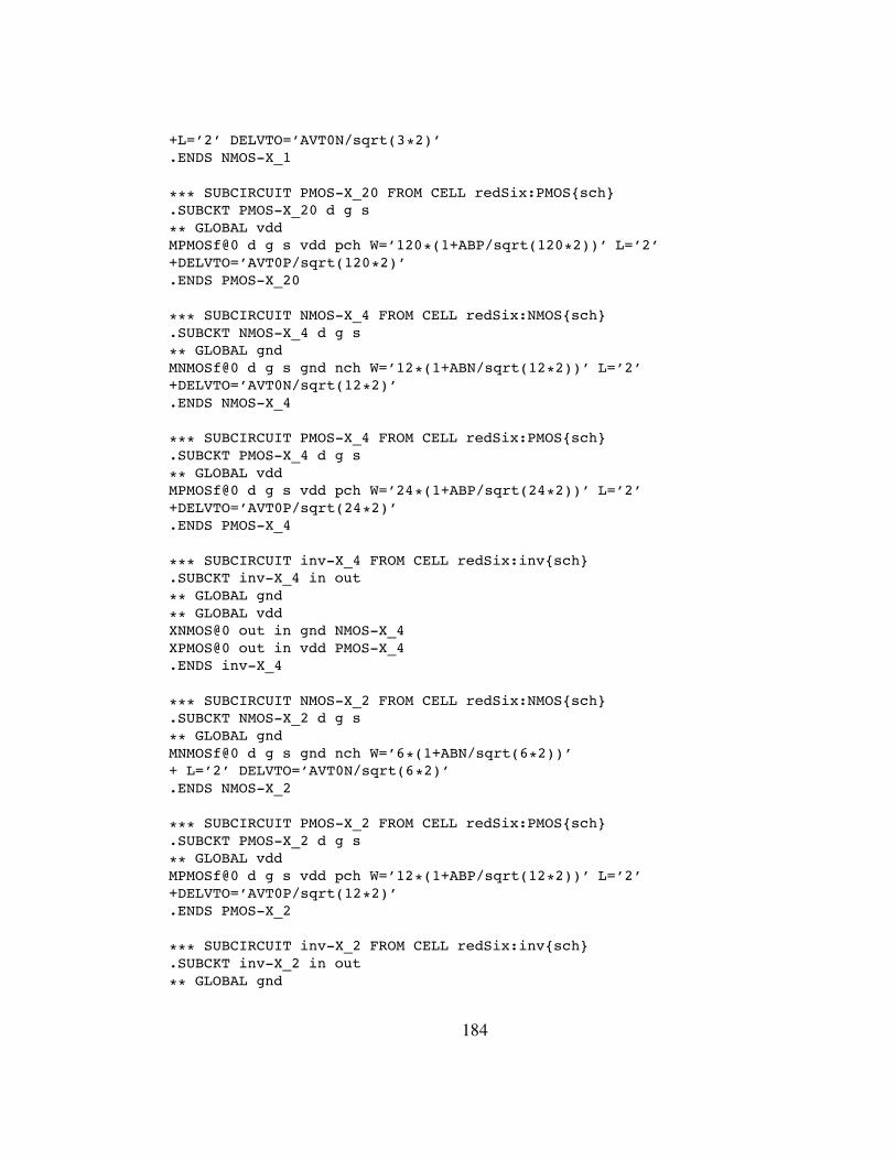
+L=’2’ DELVTO=’AVT0N/sqrt(3*2)’.ENDS NMOS-X_1
*** SUBCIRCUIT PMOS-X_20 FROM CELL redSix:PMOS{sch}.SUBCKT PMOS-X_20 d g s
** GLOBAL vddMPMOSf@0 d g s vdd pch W=’120*(1+ABP/sqrt(120*2))’ L=’2’+DELVTO=’AVT0P/sqrt(120*2)’.ENDS PMOS-X_20
*** SUBCIRCUIT NMOS-X_4 FROM CELL redSix:NMOS{sch}.SUBCKT NMOS-X_4 d g s** GLOBAL gndMNMOSf@0 d g s gnd nch W=’12*(1+ABN/sqrt(12*2))’ L=’2’+DELVTO=’AVT0N/sqrt(12*2)’.ENDS NMOS-X_4
*** SUBCIRCUIT PMOS-X_4 FROM CELL redSix:PMOS{sch}.SUBCKT PMOS-X_4 d g s
** GLOBAL vddMPMOSf@0 d g s vdd pch W=’24*(1+ABP/sqrt(24*2))’ L=’2’+DELVTO=’AVT0P/sqrt(24*2)’.ENDS PMOS-X_4
*** SUBCIRCUIT inv-X_4 FROM CELL redSix:inv{sch}.SUBCKT inv-X_4 in out
** GLOBAL gnd
** GLOBAL vddXNMOS@0 out in gnd NMOS-X_4XPMOS@0 out in vdd PMOS-X_4.ENDS inv-X_4
*** SUBCIRCUIT NMOS-X_2 FROM CELL redSix:NMOS{sch}.SUBCKT NMOS-X_2 d g s
** GLOBAL gndMNMOSf@0 d g s gnd nch W=’6*(1+ABN/sqrt(6*2))’+ L=’2’ DELVTO=’AVT0N/sqrt(6*2)’.ENDS NMOS-X_2
*** SUBCIRCUIT PMOS-X_2 FROM CELL redSix:PMOS{sch}.SUBCKT PMOS-X_2 d g s** GLOBAL vddMPMOSf@0 d g s vdd pch W=’12*(1+ABP/sqrt(12*2))’ L=’2’+DELVTO=’AVT0P/sqrt(12*2)’.ENDS PMOS-X_2
*** SUBCIRCUIT inv-X_2 FROM CELL redSix:inv{sch}.SUBCKT inv-X_2 in out
** GLOBAL gnd
184
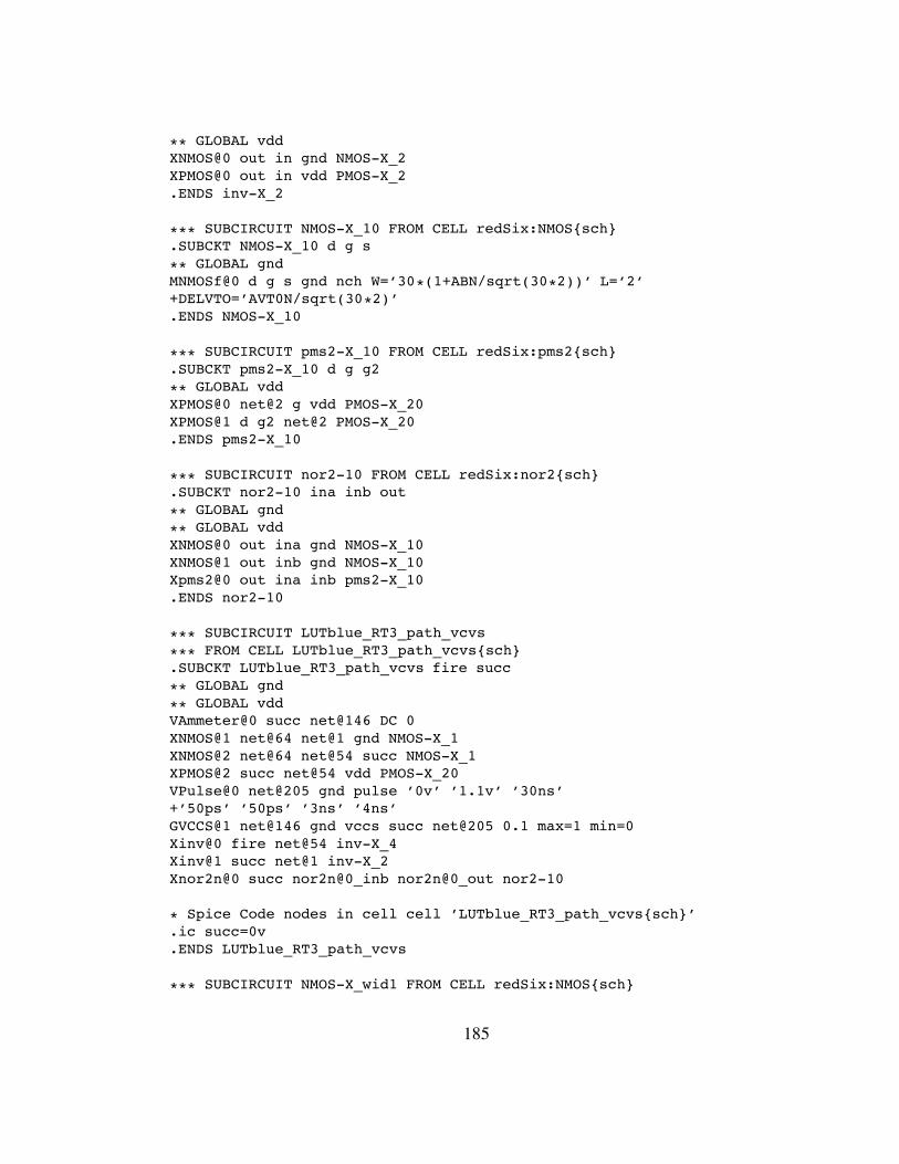
** GLOBAL vddXNMOS@0 out in gnd NMOS-X_2XPMOS@0 out in vdd PMOS-X_2.ENDS inv-X_2
*** SUBCIRCUIT NMOS-X_10 FROM CELL redSix:NMOS{sch}.SUBCKT NMOS-X_10 d g s
** GLOBAL gndMNMOSf@0 d g s gnd nch W=’30*(1+ABN/sqrt(30*2))’ L=’2’+DELVTO=’AVT0N/sqrt(30*2)’.ENDS NMOS-X_10
*** SUBCIRCUIT pms2-X_10 FROM CELL redSix:pms2{sch}.SUBCKT pms2-X_10 d g g2** GLOBAL vddXPMOS@0 net@2 g vdd PMOS-X_20XPMOS@1 d g2 net@2 PMOS-X_20.ENDS pms2-X_10
*** SUBCIRCUIT nor2-10 FROM CELL redSix:nor2{sch}.SUBCKT nor2-10 ina inb out
** GLOBAL gnd** GLOBAL vddXNMOS@0 out ina gnd NMOS-X_10XNMOS@1 out inb gnd NMOS-X_10Xpms2@0 out ina inb pms2-X_10.ENDS nor2-10
*** SUBCIRCUIT LUTblue_RT3_path_vcvs
*** FROM CELL LUTblue_RT3_path_vcvs{sch}.SUBCKT LUTblue_RT3_path_vcvs fire succ
** GLOBAL gnd
** GLOBAL vddVAmmeter@0 succ net@146 DC 0XNMOS@1 net@64 net@1 gnd NMOS-X_1XNMOS@2 net@64 net@54 succ NMOS-X_1XPMOS@2 succ net@54 vdd PMOS-X_20VPulse@0 net@205 gnd pulse ’0v’ ’1.1v’ ’30ns’+’50ps’ ’50ps’ ’3ns’ ’4ns’GVCCS@1 net@146 gnd vccs succ net@205 0.1 max=1 min=0Xinv@0 fire net@54 inv-X_4Xinv@1 succ net@1 inv-X_2Xnor2n@0 succ nor2n@0_inb nor2n@0_out nor2-10
* Spice Code nodes in cell cell ’LUTblue_RT3_path_vcvs{sch}’.ic succ=0v.ENDS LUTblue_RT3_path_vcvs
*** SUBCIRCUIT NMOS-X_wid1 FROM CELL redSix:NMOS{sch}
185
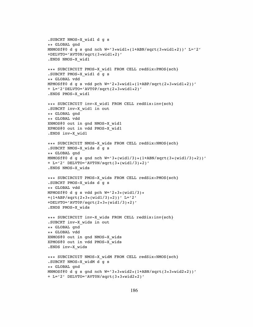
.SUBCKT NMOS-X_wid1 d g s** GLOBAL gndMNMOSf@0 d g s gnd nch W=’3*wid1*(1+ABN/sqrt(3*wid1*2))’ L=’2’+DELVTO=’AVT0N/sqrt(3*wid1*2)’.ENDS NMOS-X_wid1
*** SUBCIRCUIT PMOS-X_wid1 FROM CELL redSix:PMOS{sch}.SUBCKT PMOS-X_wid1 d g s
** GLOBAL vddMPMOSf@0 d g s vdd pch W=’2*3*wid1*(1+ABP/sqrt(2*3*wid1*2))’+ L=’2’DELVTO=’AVT0P/sqrt(2*3*wid1*2)’.ENDS PMOS-X_wid1
*** SUBCIRCUIT inv-X_wid1 FROM CELL redSix:inv{sch}.SUBCKT inv-X_wid1 in out
** GLOBAL gnd
** GLOBAL vddXNMOS@0 out in gnd NMOS-X_wid1XPMOS@0 out in vdd PMOS-X_wid1.ENDS inv-X_wid1
*** SUBCIRCUIT NMOS-X_wids FROM CELL redSix:NMOS{sch}.SUBCKT NMOS-X_wids d g s
** GLOBAL gndMNMOSf@0 d g s gnd nch W=’3*(wid1/3)*(1+ABN/sqrt(3*(wid1/3)*2))’+ L=’2’ DELVTO=’AVT0N/sqrt(3*(wid1/3)*2)’.ENDS NMOS-X_wids
*** SUBCIRCUIT PMOS-X_wids FROM CELL redSix:PMOS{sch}.SUBCKT PMOS-X_wids d g s** GLOBAL vddMPMOSf@0 d g s vdd pch W=’2*3*(wid1/3)*+(1+ABP/sqrt(2*3*(wid1/3)*2))’ L=’2’+DELVTO=’AVT0P/sqrt(2*3*(wid1/3)*2)’.ENDS PMOS-X_wids
*** SUBCIRCUIT inv-X_wids FROM CELL redSix:inv{sch}.SUBCKT inv-X_wids in out** GLOBAL gnd
** GLOBAL vddXNMOS@0 out in gnd NMOS-X_widsXPMOS@0 out in vdd PMOS-X_wids.ENDS inv-X_wids
*** SUBCIRCUIT NMOS-X_widM FROM CELL redSix:NMOS{sch}.SUBCKT NMOS-X_widM d g s** GLOBAL gndMNMOSf@0 d g s gnd nch W=’3*3*wid2*(1+ABN/sqrt(3*3*wid2*2))’+ L=’2’ DELVTO=’AVT0N/sqrt(3*3*wid2*2)’
186
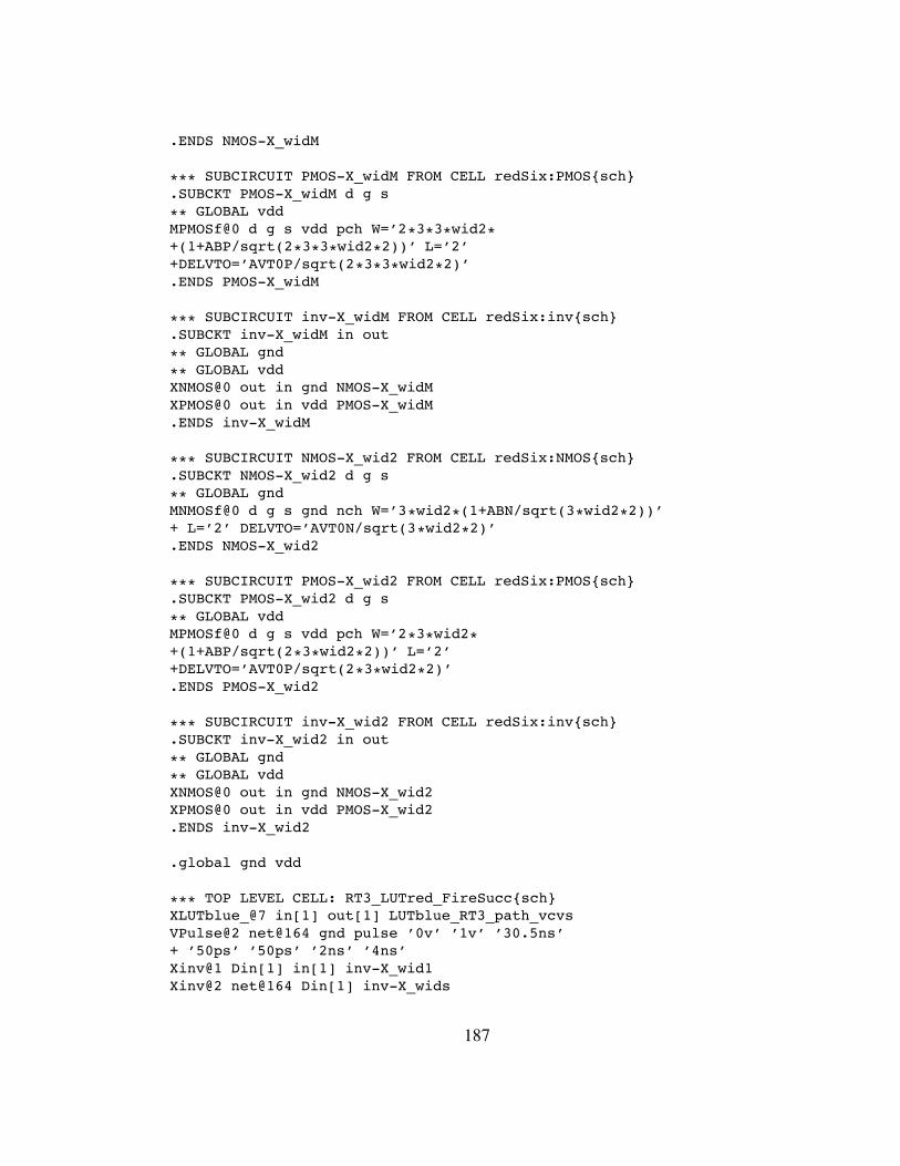
.ENDS NMOS-X_widM
*** SUBCIRCUIT PMOS-X_widM FROM CELL redSix:PMOS{sch}.SUBCKT PMOS-X_widM d g s** GLOBAL vddMPMOSf@0 d g s vdd pch W=’2*3*3*wid2*+(1+ABP/sqrt(2*3*3*wid2*2))’ L=’2’+DELVTO=’AVT0P/sqrt(2*3*3*wid2*2)’.ENDS PMOS-X_widM
*** SUBCIRCUIT inv-X_widM FROM CELL redSix:inv{sch}.SUBCKT inv-X_widM in out** GLOBAL gnd
** GLOBAL vddXNMOS@0 out in gnd NMOS-X_widMXPMOS@0 out in vdd PMOS-X_widM.ENDS inv-X_widM
*** SUBCIRCUIT NMOS-X_wid2 FROM CELL redSix:NMOS{sch}.SUBCKT NMOS-X_wid2 d g s** GLOBAL gndMNMOSf@0 d g s gnd nch W=’3*wid2*(1+ABN/sqrt(3*wid2*2))’+ L=’2’ DELVTO=’AVT0N/sqrt(3*wid2*2)’.ENDS NMOS-X_wid2
*** SUBCIRCUIT PMOS-X_wid2 FROM CELL redSix:PMOS{sch}.SUBCKT PMOS-X_wid2 d g s
** GLOBAL vddMPMOSf@0 d g s vdd pch W=’2*3*wid2*+(1+ABP/sqrt(2*3*wid2*2))’ L=’2’+DELVTO=’AVT0P/sqrt(2*3*wid2*2)’.ENDS PMOS-X_wid2
*** SUBCIRCUIT inv-X_wid2 FROM CELL redSix:inv{sch}.SUBCKT inv-X_wid2 in out
** GLOBAL gnd** GLOBAL vddXNMOS@0 out in gnd NMOS-X_wid2XPMOS@0 out in vdd PMOS-X_wid2.ENDS inv-X_wid2
.global gnd vdd
*** TOP LEVEL CELL: RT3_LUTred_FireSucc{sch}XLUTblue_@7 in[1] out[1] LUTblue_RT3_path_vcvsVPulse@2 net@164 gnd pulse ’0v’ ’1v’ ’30.5ns’+ ’50ps’ ’50ps’ ’2ns’ ’4ns’Xinv@1 Din[1] in[1] inv-X_wid1Xinv@2 net@164 Din[1] inv-X_wids
187

Xinv@3 net@64 inv@3_out inv-X_widMXinv@4 out[1] net@64 inv-X_wid2
* Trailer cards are described in this file:.include ’/u/mettalag/models/Models_90nm/MOSIS_trailer_ARC_3.hsp’.END
188

F.2 SPICE Simulation Setup File: HEADERHere is the basic file with default simulation parameters for SPICE. Its extension is‘.hsp’. It contains a pointer to the 90nm CMOS process models for our GasP designs.We use the library with typical (TT) Process, Voltage and Temperature (PVT) settings.
***************************************************************** Header File for Simulation with 90nm MOSIS Transistor Models*****************************************************************
********************************************************************************************************************************.LIB ’/stash/arc/models/tsmc90/hspice/cmn90g_2d5_lk_v1d0.l’ TT
*.LIB ’/stash/arc/models/tsmc90/hspice/cmn90g_1d8_3d3_lk_v1d0.l’ TT
***************************************************************** Options and Parameters****************************************************************.OPTION nomod POST.OPTION SCALE=50n.OPTION CAPTAB.PARAM hdifp=0.PARAM hdifn=0.PARAM ABN=0.PARAM ABP=0.PARAM AVT0P=0.PARAM AVT0N=0.PARAM SUPPLY=1V
***************************************************************** Netlist****************************************************************
189
F.3 SPICE Simulation Setup File: TRAILERBelow follows the SPICE trailer file with the .DATA sweep, transient analysis, andmeasurement details for the simulation environment in Figure 4.15, page 72, and in theblack box schematics of Figure 4.10, page 61. We generate look up tables for relativetiming paths LUTred:FIREi+SUCCi+ and LUTblue:FIREi+SUCCi+. To do so, wesweep driver size wid1 and load size wid2 we measure the voltage on in[1], out[1].
***************************************************************** Trailer File For Simulation with 90nm MOSIS Transistor Models
****************************************************************** Power Supply
****************************************************************Vdd vdd gnd ’SUPPLY’
************************* Step size and run time.tran 1ps 100ns sweep data=mysweep
.data mysweep wid1 wid2
8 106 104 103 10
8 336 334 333 33
8 566 564 563 56
8 786 784 783 78
8 1006 1004 1003 100
.enddata
190

.measure trise_i_1+ trig v(in[1]) val=’0.2*SUPPLY’ rise=3+ targ v(in[1]) val=’0.8*SUPPLY’ rise=3
.measure trise_o_1+ trig v(out[1]) val=’0.2*SUPPLY’ rise=3+ targ v(out[1]) val=’0.8*SUPPLY’ rise=3
.measure tr_delay+ trig v(in[1]) val=’0.5*SUPPLY’ rise=3+ targ v(out[1]) val=’0.5*SUPPLY’ rise=3
***********************
191
F.4 SPICE Output FileBelow is the SPICE output file with the look up table results for the two relative tim-ing paths LUTred:FIREi+SUCCi+ and LUTblue:FIREi+SUCCi+, as measured for theschematic of Figure 4.15, page 72, and the black box schematics of Figure 4.10, page 61.The file extension is ‘.mt0’.The file contains the 4#5 wid1#wid2 sweep index, i.e. index 1 through 20. Per sweep,the file shows the sizes of sweep variables wid1 and wid2 and the measured timingresults in seconds. We measure the following timing information:
• trise i 1, the transition rise time, a.k.a. slope or slew time, on input in[1]• trise o 1, the transition rise time, a.k.a. slope or slew time, on output out[1]• tr delay, input-to-output delay for the rising transition from in[1] to out[1]
Note: the additional process parameters temper and alter# can be ignored.
$DATA1 SOURCE=’HSPICE’ VERSION=’C-2009.03 64-BIT’.TITLE ’ *** spice deck for cell rt3_firesucc{sch} from library’index wid1 wid2 trise_i_1
trise_o_1 tr_delay temperalter#
1.0000 8.0000 10.0000 1.171e-111.517e-11 2.892e-11 25.0000
1.00002.0000 6.0000 10.0000 1.269e-11
1.488e-11 2.896e-11 25.00001.0000
3.0000 4.0000 10.0000 1.538e-111.540e-11 2.997e-11 25.0000
1.00004.0000 3.0000 10.0000 1.720e-11
1.602e-11 3.095e-11 25.00001.0000
5.0000 8.0000 33.0000 1.173e-112.065e-11 3.313e-11 25.0000
1.00006.0000 6.0000 33.0000 1.268e-11
2.082e-11 3.366e-11 25.00001.0000
7.0000 4.0000 33.0000 1.521e-112.126e-11 3.473e-11 25.0000
1.00008.0000 3.0000 33.0000 1.739e-11
2.140e-11 3.561e-11 25.00001.0000
9.0000 8.0000 56.0000 1.124e-112.696e-11 3.710e-11 25.0000
1.0000
192

10.0000 6.0000 56.0000 1.268e-112.742e-11 3.778e-11 25.0000
1.000011.0000 4.0000 56.0000 1.521e-11
2.756e-11 3.877e-11 25.00001.0000
12.0000 3.0000 56.0000 1.745e-112.773e-11 3.987e-11 25.0000
1.000013.0000 8.0000 78.0000 1.151e-11
3.414e-11 4.101e-11 25.00001.0000
14.0000 6.0000 78.0000 1.256e-113.388e-11 4.158e-11 25.0000
1.000015.0000 4.0000 78.0000 1.528e-11
3.399e-11 4.236e-11 25.00001.0000
16.0000 3.0000 78.0000 1.712e-113.404e-11 4.338e-11 25.0000
1.000017.0000 8.0000 100.0000 1.454e-11
4.048e-11 4.425e-11 25.00001.0000
18.0000 6.0000 100.0000 1.267e-114.038e-11 4.528e-11 25.0000
1.000019.0000 4.0000 100.0000 1.486e-11
4.043e-11 4.636e-11 25.00001.0000
20.0000 3.0000 100.0000 1.740e-114.095e-11 4.724e-11 25.0000
1.0000
*********************************************************
193
Appendix G
SPICE FILES FOR FIGURE 4.11 AND LUTblue/green:FIREi+PREDi"
Ideally, the SPICE simulations for Figure 4.18 on page 77 will run the green path formaximum delay conditions by using slow PVT library setting, and they wil run the bluepath for minimum delay conditions by using fast settings. We show only one simulation(covering both paths) using typical Process, Voltage, Temperature (PVT) settings.
G.1 SPICE NetlistThe SPICE netlist file generated from the design schematics in Electric has the detailsof all the components and devices used in the schematics of Figure 4.18 on page 77and in the black box schematics of Figure 4.11 on page 63. The black box belongs torelative timing paths LUTblue:FIREi+PREDi" and LUTgreen:FIREi+PREDi". Thesweep parameters wid1 and wid2 are the sizes of the driver and load inverters. Thisconfiguration has two pulse generators, one for signal FIREi to start each measurement,one for signal FIRE CSi to reset the output signal PREDi prior to the next measurement.The file extension is ‘.spi’.
*** SPICE deck for cell RT5_LUTred_FirePred{sch} from library
*LookUpTable_Thesis*** Created on Wed Jul 21, 2010 21:21:49
*** Last revised on Mon Aug 09, 2010 17:16:40*** Written on Mon Aug 09, 2010 17:16:46 by Electric
*** VLSI Design System, version 9.00d
*** Layout tech: mocmos, foundry MOSIS*** UC SPICE *** , MIN_RESIST 4.0, MIN_CAPAC 0.1FF.OPTIONS NOMOD NOPAGE
* Model cards are described in this file:.include ’/u/mettalag/models/Models_90nm/MOSIS_90nm_header_ARC.hsp’
*** SUBCIRCUIT NMOS-X_20 FROM CELL redSix:NMOS{sch}.SUBCKT NMOS-X_20 d g s
** GLOBAL gndMNMOSf@0 d g s gnd nch W=’60*(1+ABN/sqrt(60*2))’ L=’2’+DELVTO=’AVT0N/sqrt(60*2)’
194
.ENDS NMOS-X_2
*** SUBCIRCUIT PMOS-X_1 FROM CELL redSix:PMOS{sch}.SUBCKT PMOS-X_1 d g s** GLOBAL vddMPMOSf@0 d g s vdd pch W=’6*(1+ABP/sqrt(6*2))’ L=’2’+DELVTO=’AVT0P/sqrt(6*2)’.ENDS PMOS-X_1
*** SUBCIRCUIT NMOS-X_5 FROM CELL redSix:NMOS{sch}.SUBCKT NMOS-X_5 d g s
** GLOBAL gndMNMOSf@0 d g s gnd nch W=’15*(1+ABN/sqrt(15*2))’ L=’2’+DELVTO=’AVT0N/sqrt(15*2)’.ENDS NMOS-X_5
*** SUBCIRCUIT PMOS-X_5 FROM CELL redSix:PMOS{sch}.SUBCKT PMOS-X_5 d g s
** GLOBAL vddMPMOSf@0 d g s vdd pch W=’30*(1+ABP/sqrt(30*2))’ L=’2’+DELVTO=’AVT0P/sqrt(30*2)’.ENDS PMOS-X_5
*** SUBCIRCUIT inv-X_5 FROM CELL redSix:inv{sch}.SUBCKT inv-X_5 in out** GLOBAL gnd
** GLOBAL vddXNMOS@0 out in gnd NMOS-X_5XPMOS@0 out in vdd PMOS-X_5.ENDS inv-X_5
*** SUBCIRCUIT NMOS-X_2 FROM CELL redSix:NMOS{sch}.SUBCKT NMOS-X_2 d g s** GLOBAL gndMNMOSf@0 d g s gnd nch W=’6*(1+ABN/sqrt(6*2))’+ L=’2’ DELVTO=’AVT0N/sqrt(6*2)’.ENDS NMOS-X_2
*** SUBCIRCUIT PMOS-X_2 FROM CELL redSix:PMOS{sch}.SUBCKT PMOS-X_2 d g s
** GLOBAL vddMPMOSf@0 d g s vdd pch W=’12*(1+ABP/sqrt(12*2))’ L=’2’+DELVTO=’AVT0P/sqrt(12*2)’.ENDS PMOS-X_2
*** SUBCIRCUIT inv-X_2 FROM CELL redSix:inv{sch}.SUBCKT inv-X_2 in out
** GLOBAL gnd
** GLOBAL vdd
195
XNMOS@0 out in gnd NMOS-X_2XPMOS@0 out in vdd PMOS-X_2.ENDS inv-X_2
*** SUBCIRCUIT LUTblue_RT5_path FROM CELL LUTblue_RT5_path{sch}.SUBCKT LUTblue_RT5_path fire pred** GLOBAL gnd
** GLOBAL vddVAmmeter@0 pred net@70 DC 0XNMOS@0 pred fire gnd NMOS-X_20XPMOS@0 net@48 net@46 vdd PMOS-X_1XPMOS@1 net@48 PMOS@1_g pred PMOS-X_1VPulse@0 net@106 gnd pulse ’1v’ ’-0.5v’ ’30ns’ ’50ps’+ ’50ps’ ’3ns’ ’4ns’GVCCS@0 net@70 gnd vccs pred net@106 0.1 max=0 min=-1Xinv@2 pred inv@2_out inv-X_5Xinv@5 pred net@46 inv-X_2
* Spice Code nodes in cell cell ’LUTblue_RT5_path{sch}’.ic net@83=1v.ENDS LUTblue_RT5_path
*** SUBCIRCUIT NMOS-X_wid1 FROM CELL redSix:NMOS{sch}.SUBCKT NMOS-X_wid1 d g s
** GLOBAL gndMNMOSf@0 d g s gnd nch W=’3*wid1*(1+ABN/sqrt(3*wid1*2))’+ L=’2’DELVTO=’AVT0N/sqrt(3*wid1*2)’.ENDS NMOS-X_wid1
*** SUBCIRCUIT PMOS-X_wid1 FROM CELL redSix:PMOS{sch}.SUBCKT PMOS-X_wid1 d g s
** GLOBAL vddMPMOSf@0 d g s vdd pch W=’2*3*wid1*(1+ABP/sqrt(2*3*wid1*2))’+ L=’2’DELVTO=’AVT0P/sqrt(2*3*wid1*2)’.ENDS PMOS-X_wid1
*** SUBCIRCUIT inv-X_wid1 FROM CELL redSix:inv{sch}.SUBCKT inv-X_wid1 in out** GLOBAL gnd
** GLOBAL vddXNMOS@0 out in gnd NMOS-X_wid1XPMOS@0 out in vdd PMOS-X_wid1.ENDS inv-X_wid1
*** SUBCIRCUIT NMOS-X_wids FROM CELL redSix:NMOS{sch}.SUBCKT NMOS-X_wids d g s** GLOBAL gndMNMOSf@0 d g s gnd nch W=’3*(wid1/3)*(1+ABN/sqrt(3*(wid1/3)*2))’+ L=’2’ DELVTO=’AVT0N/sqrt(3*(wid1/3)*2)’
196
.ENDS NMOS-X_wids
*** SUBCIRCUIT PMOS-X_wids FROM CELL redSix:PMOS{sch}.SUBCKT PMOS-X_wids d g s** GLOBAL vddMPMOSf@0 d g s vdd pch W=’2*3*(wid1/3)*+(1+ABP/sqrt(2*3*(wid1/3)*2))’ L=’2’+DELVTO=’AVT0P/sqrt(2*3*(wid1/3)*2)’.ENDS PMOS-X_wids
*** SUBCIRCUIT inv-X_wids FROM CELL redSix:inv{sch}.SUBCKT inv-X_wids in out** GLOBAL gnd
** GLOBAL vddXNMOS@0 out in gnd NMOS-X_widsXPMOS@0 out in vdd PMOS-X_wids.ENDS inv-X_wids
*** SUBCIRCUIT NMOS-X_widM FROM CELL redSix:NMOS{sch}.SUBCKT NMOS-X_widM d g s** GLOBAL gndMNMOSf@0 d g s gnd nch W=’3*3*wid2*(1+ABN/sqrt(3*3*wid2*2))’+ L=’2’ DELVTO=’AVT0N/sqrt(3*3*wid2*2)’.ENDS NMOS-X_widM
*** SUBCIRCUIT PMOS-X_widM FROM CELL redSix:PMOS{sch}.SUBCKT PMOS-X_widM d g s
** GLOBAL vddMPMOSf@0 d g s vdd pch W=’2*3*3*wid2*+(1+ABP/sqrt(2*3*3*wid2*2))’ L=’2’+DELVTO=’AVT0P/sqrt(2*3*3*wid2*2)’.ENDS PMOS-X_widM
*** SUBCIRCUIT inv-X_widM FROM CELL redSix:inv{sch}.SUBCKT inv-X_widM in out
** GLOBAL gnd** GLOBAL vddXNMOS@0 out in gnd NMOS-X_widMXPMOS@0 out in vdd PMOS-X_widM.ENDS inv-X_widM
*** SUBCIRCUIT NMOS-X_wid2 FROM CELL redSix:NMOS{sch}.SUBCKT NMOS-X_wid2 d g s
** GLOBAL gndMNMOSf@0 d g s gnd nch W=’3*wid2*(1+ABN/sqrt(3*wid2*2))’+ L=’2’ DELVTO=’AVT0N/sqrt(3*wid2*2)’.ENDS NMOS-X_wid2
*** SUBCIRCUIT PMOS-X_wid2 FROM CELL redSix:PMOS{sch}
197
.SUBCKT PMOS-X_wid2 d g s** GLOBAL vddMPMOSf@0 d g s vdd pch W=’2*3*wid2*+(1+ABP/sqrt(2*3*wid2*2))’ L=’2’+DELVTO=’AVT0P/sqrt(2*3*wid2*2)’.ENDS PMOS-X_wid2
*** SUBCIRCUIT inv-X_wid2 FROM CELL redSix:inv{sch}.SUBCKT inv-X_wid2 in out** GLOBAL gnd
** GLOBAL vddXNMOS@0 out in gnd NMOS-X_wid2XPMOS@0 out in vdd PMOS-X_wid2.ENDS inv-X_wid2
.global gnd vdd
*** TOP LEVEL CELL: RT5_LUTred_FirePred{sch}XLUTblue_@7 in[1] out[1] LUTblue_RT5_pathVPulse@1 net@156 gnd pulse ’0v’ ’1v’ ’30.5ns’+’50ps’ ’50ps’ ’2ns’ ’4ns’Xinv@1 Din[1] in[1] inv-X_wid1Xinv@2 net@156 Din[1] inv-X_widsXinv@3 net@64 inv@3_out inv-X_widMXinv@4 out[1] net@64 inv-X_wid2* Trailer cards are described in this file:.include ’/u/mettalag/models/Models_90nm/MOSIS_trailer_ARC_5.hsp’.END
198

G.2 SPICE Simulation Setup File: HEADERHere is the basic file with default simulation parameters for SPICE. Its extension is‘.hsp’. It contains a pointer to the 90nm CMOS process models for our GasP designs.We use the library with typical (TT) Process, Voltage and Temperature (PVT) settings.
***************************************************************** Header File for Simulation with 90nm MOSIS Transistor Models*****************************************************************
********************************************************************************************************************************.LIB ’/stash/arc/models/tsmc90/hspice/cmn90g_2d5_lk_v1d0.l’ TT
*.LIB ’/stash/arc/models/tsmc90/hspice/cmn90g_1d8_3d3_lk_v1d0.l’ TT
***************************************************************** Options and Parameters****************************************************************.OPTION nomod POST.OPTION SCALE=50n.OPTION CAPTAB.PARAM hdifp=0.PARAM hdifn=0.PARAM ABN=0.PARAM ABP=0.PARAM AVT0P=0.PARAM AVT0N=0.PARAM SUPPLY=1V
***************************************************************** Netlist****************************************************************
199
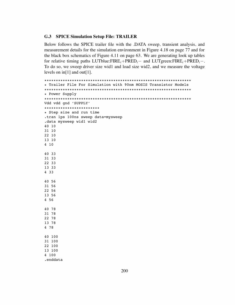
G.3 SPICE Simulation Setup File: TRAILERBelow follows the SPICE trailer file with the .DATA sweep, transient analysis, andmeasurement details for the simulation environment in Figure 4.18 on page 77 and forthe black box schematics of Figure 4.11 on page 63. We are generating look up tablesfor relative timing paths LUTblue:FIREi+PREDi" and LUTgreen:FIREi+PREDi".To do so, we sweep driver size wid1 and load size wid2, and we measure the voltagelevels on in[1] and out[1].
***************************************************************** Trailer File For Simulation with 90nm MOSIS Transistor Models
***************************************************************** Power Supply
****************************************************************Vdd vdd gnd ’SUPPLY’************************* Step size and run time.tran 1ps 100ns sweep data=mysweep.data mysweep wid1 wid240 1031 1022 1013 104 10
40 3331 3322 3313 334 33
40 5631 5622 5613 564 56
40 7831 7822 7813 784 78
40 10031 10022 10013 1004 100.enddata
200
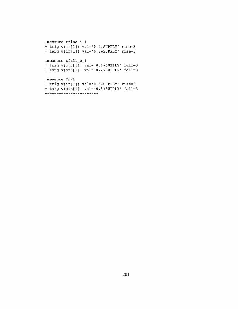
.measure trise_i_1+ trig v(in[1]) val=’0.2*SUPPLY’ rise=3+ targ v(in[1]) val=’0.8*SUPPLY’ rise=3
.measure tfall_o_1+ trig v(out[1]) val=’0.8*SUPPLY’ fall=3+ targ v(out[1]) val=’0.2*SUPPLY’ fall=3
.measure TpHL+ trig v(in[1]) val=’0.5*SUPPLY’ rise=3+ targ v(out[1]) val=’0.5*SUPPLY’ fall=3***********************
201
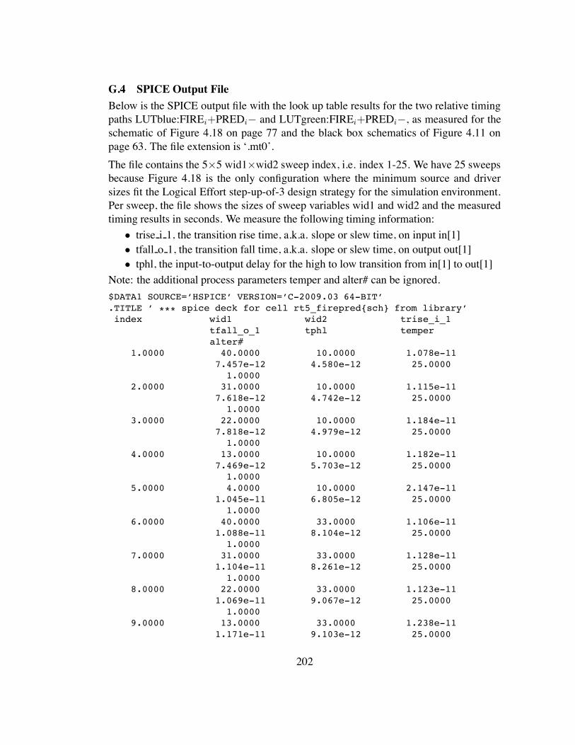
G.4 SPICE Output FileBelow is the SPICE output file with the look up table results for the two relative timingpaths LUTblue:FIREi+PREDi" and LUTgreen:FIREi+PREDi", as measured for theschematic of Figure 4.18 on page 77 and the black box schematics of Figure 4.11 onpage 63. The file extension is ‘.mt0’.The file contains the 5#5 wid1#wid2 sweep index, i.e. index 1-25. We have 25 sweepsbecause Figure 4.18 is the only configuration where the minimum source and driversizes fit the Logical Effort step-up-of-3 design strategy for the simulation environment.Per sweep, the file shows the sizes of sweep variables wid1 and wid2 and the measuredtiming results in seconds. We measure the following timing information:
• trise i 1, the transition rise time, a.k.a. slope or slew time, on input in[1]• tfall o 1, the transition fall time, a.k.a. slope or slew time, on output out[1]• tphl, the input-to-output delay for the high to low transition from in[1] to out[1]
Note: the additional process parameters temper and alter# can be ignored.$DATA1 SOURCE=’HSPICE’ VERSION=’C-2009.03 64-BIT’.TITLE ’ *** spice deck for cell rt5_firepred{sch} from library’index wid1 wid2 trise_i_1
tfall_o_1 tphl temperalter#
1.0000 40.0000 10.0000 1.078e-117.457e-12 4.580e-12 25.0000
1.00002.0000 31.0000 10.0000 1.115e-11
7.618e-12 4.742e-12 25.00001.0000
3.0000 22.0000 10.0000 1.184e-117.818e-12 4.979e-12 25.0000
1.00004.0000 13.0000 10.0000 1.182e-11
7.469e-12 5.703e-12 25.00001.0000
5.0000 4.0000 10.0000 2.147e-111.045e-11 6.805e-12 25.0000
1.00006.0000 40.0000 33.0000 1.106e-11
1.088e-11 8.104e-12 25.00001.0000
7.0000 31.0000 33.0000 1.128e-111.104e-11 8.261e-12 25.0000
1.00008.0000 22.0000 33.0000 1.123e-11
1.069e-11 9.067e-12 25.00001.0000
9.0000 13.0000 33.0000 1.238e-111.171e-11 9.103e-12 25.0000
202
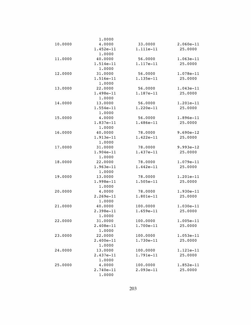
1.000010.0000 4.0000 33.0000 2.060e-11
1.452e-11 1.111e-11 25.00001.0000
11.0000 40.0000 56.0000 1.063e-111.514e-11 1.117e-11 25.0000
1.000012.0000 31.0000 56.0000 1.078e-11
1.516e-11 1.135e-11 25.00001.0000
13.0000 22.0000 56.0000 1.043e-111.498e-11 1.187e-11 25.0000
1.000014.0000 13.0000 56.0000 1.201e-11
1.554e-11 1.220e-11 25.00001.0000
15.0000 4.0000 56.0000 1.896e-111.837e-11 1.486e-11 25.0000
1.000016.0000 40.0000 78.0000 9.690e-12
1.913e-11 1.422e-11 25.00001.0000
17.0000 31.0000 78.0000 9.993e-121.904e-11 1.437e-11 25.0000
1.000018.0000 22.0000 78.0000 1.079e-11
1.963e-11 1.442e-11 25.00001.0000
19.0000 13.0000 78.0000 1.201e-111.998e-11 1.505e-11 25.0000
1.000020.0000 4.0000 78.0000 1.930e-11
2.269e-11 1.801e-11 25.00001.0000
21.0000 40.0000 100.0000 1.030e-112.398e-11 1.659e-11 25.0000
1.000022.0000 31.0000 100.0000 1.005e-11
2.408e-11 1.700e-11 25.00001.0000
23.0000 22.0000 100.0000 1.053e-112.400e-11 1.730e-11 25.0000
1.000024.0000 13.0000 100.0000 1.121e-11
2.437e-11 1.791e-11 25.00001.0000
25.0000 4.0000 100.0000 1.852e-112.740e-11 2.093e-11 25.0000
1.0000
203
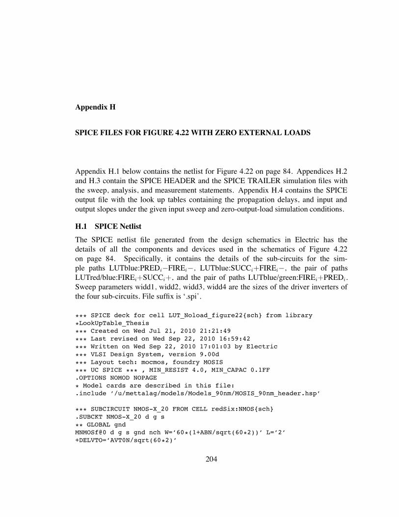
Appendix H
SPICE FILES FOR FIGURE 4.22 WITH ZERO EXTERNAL LOADS
Appendix H.1 below contains the netlist for Figure 4.22 on page 84. Appendices H.2and H.3 contain the SPICE HEADER and the SPICE TRAILER simulation files withthe sweep, analysis, and measurement statements. Appendix H.4 contains the SPICEoutput file with the look up tables containing the propagation delays, and input andoutput slopes under the given input sweep and zero-output-load simulation conditions.
H.1 SPICE NetlistThe SPICE netlist file generated from the design schematics in Electric has thedetails of all the components and devices used in the schematics of Figure 4.22on page 84. Specifically, it contains the details of the sub-circuits for the sim-ple paths LUTblue:PREDi"FIREi", LUTblue:SUCCi+FIREi", the pair of pathsLUTred/blue:FIREi+SUCCi+, and the pair of paths LUTblue/green:FIREi+PREDi.Sweep parameters widd1, widd2, widd3, widd4 are the sizes of the driver inverters ofthe four sub-circuits. File suffix is ‘.spi’.
*** SPICE deck for cell LUT_Noload_figure22{sch} from library
*LookUpTable_Thesis*** Created on Wed Jul 21, 2010 21:21:49
*** Last revised on Wed Sep 22, 2010 16:59:42*** Written on Wed Sep 22, 2010 17:01:03 by Electric
*** VLSI Design System, version 9.00d
*** Layout tech: mocmos, foundry MOSIS*** UC SPICE *** , MIN_RESIST 4.0, MIN_CAPAC 0.1FF.OPTIONS NOMOD NOPAGE
* Model cards are described in this file:.include ’/u/mettalag/models/Models_90nm/MOSIS_90nm_header.hsp’
*** SUBCIRCUIT NMOS-X_20 FROM CELL redSix:NMOS{sch}.SUBCKT NMOS-X_20 d g s
** GLOBAL gndMNMOSf@0 d g s gnd nch W=’60*(1+ABN/sqrt(60*2))’ L=’2’+DELVTO=’AVT0N/sqrt(60*2)’
204
.ENDS NMOS-X_20
*** SUBCIRCUIT PMOS-X_1 FROM CELL redSix:PMOS{sch}.SUBCKT PMOS-X_1 d g s** GLOBAL vddMPMOSf@0 d g s vdd pch W=’6*(1+ABP/sqrt(6*2))’ L=’2’+DELVTO=’AVT0P/sqrt(6*2)’.ENDS PMOS-X_1
*** SUBCIRCUIT NMOS-X_30 FROM CELL redSix:NMOS{sch}.SUBCKT NMOS-X_30 d g s
** GLOBAL gndMNMOSf@0 d g s gnd nch W=’90*(1+ABN/sqrt(90*2))’ L=’2’+DELVTO=’AVT0N/sqrt(90*2)’.ENDS NMOS-X_30
*** SUBCIRCUIT PMOS-X_30 FROM CELL redSix:PMOS{sch}.SUBCKT PMOS-X_30 d g s
** GLOBAL vddMPMOSf@0 d g s vdd pch W=’180*(1+ABP/sqrt(180*2))’ L=’2’+DELVTO=’AVT0P/sqrt(180*2)’.ENDS PMOS-X_30
*** SUBCIRCUIT inv-X_30 FROM CELL redSix:inv{sch}.SUBCKT inv-X_30 in out** GLOBAL gnd
** GLOBAL vddXNMOS@0 out in gnd NMOS-X_30XPMOS@0 out in vdd PMOS-X_30.ENDS inv-X_30
*** SUBCIRCUIT NMOS-X_80 FROM CELL redSix:NMOS{sch}.SUBCKT NMOS-X_80 d g s** GLOBAL gndMNMOSf@0 d g s gnd nch W=’240*(1+ABN/sqrt(240*2))’ L=’2’+DELVTO=’AVT0N/sqrt(240*2)’.ENDS NMOS-X_80
*** SUBCIRCUIT PMOS-X_80 FROM CELL redSix:PMOS{sch}.SUBCKT PMOS-X_80 d g s
** GLOBAL vddMPMOSf@0 d g s vdd pch W=’480*(1+ABP/sqrt(480*2))’ L=’2’+DELVTO=’AVT0P/sqrt(480*2)’.ENDS PMOS-X_80
*** SUBCIRCUIT inv-X_80 FROM CELL redSix:inv{sch}.SUBCKT inv-X_80 in out
** GLOBAL gnd
** GLOBAL vdd
205
XNMOS@0 out in gnd NMOS-X_80XPMOS@0 out in vdd PMOS-X_80.ENDS inv-X_80
*** SUBCIRCUIT NMOS-X_5 FROM CELL redSix:NMOS{sch}.SUBCKT NMOS-X_5 d g s** GLOBAL gndMNMOSf@0 d g s gnd nch W=’15*(1+ABN/sqrt(15*2))’ L=’2’+DELVTO=’AVT0N/sqrt(15*2)’.ENDS NMOS-X_5
*** SUBCIRCUIT PMOS-X_5 FROM CELL redSix:PMOS{sch}.SUBCKT PMOS-X_5 d g s
** GLOBAL vddMPMOSf@0 d g s vdd pch W=’30*(1+ABP/sqrt(30*2))’ L=’2’+DELVTO=’AVT0P/sqrt(30*2)’.ENDS PMOS-X_5
*** SUBCIRCUIT inv-X_5 FROM CELL redSix:inv{sch}.SUBCKT inv-X_5 in out** GLOBAL gnd
** GLOBAL vddXNMOS@0 out in gnd NMOS-X_5XPMOS@0 out in vdd PMOS-X_5.ENDS inv-X_5
*** SUBCIRCUIT NMOS-X_2 FROM CELL redSix:NMOS{sch}.SUBCKT NMOS-X_2 d g s** GLOBAL gndMNMOSf@0 d g s gnd nch W=’6*(1+ABN/sqrt(6*2))’+ L=’2’ DELVTO=’AVT0N/sqrt(6*2)’.ENDS NMOS-X_2
*** SUBCIRCUIT PMOS-X_2 FROM CELL redSix:PMOS{sch}.SUBCKT PMOS-X_2 d g s
** GLOBAL vddMPMOSf@0 d g s vdd pch W=’12*(1+ABP/sqrt(12*2))’+ L=’2’ DELVTO=’AVT0P/sqrt(12*2)’.ENDS PMOS-X_2
*** SUBCIRCUIT inv-X_2 FROM CELL redSix:inv{sch}.SUBCKT inv-X_2 in out
** GLOBAL gnd
** GLOBAL vddXNMOS@0 out in gnd NMOS-X_2XPMOS@0 out in vdd PMOS-X_2.ENDS inv-X_2
*** SUBCIRCUIT NMOS-X_10 FROM CELL redSix:NMOS{sch}
206
.SUBCKT NMOS-X_10 d g s** GLOBAL gndMNMOSf@0 d g s gnd nch W=’30*(1+ABN/sqrt(30*2))’ L=’2’+DELVTO=’AVT0N/sqrt(30*2)’.ENDS NMOS-X_10
*** SUBCIRCUIT PMOS-X_20 FROM CELL redSix:PMOS{sch}.SUBCKT PMOS-X_20 d g s
** GLOBAL vddMPMOSf@0 d g s vdd pch W=’120*(1+ABP/sqrt(120*2))’ L=’2’+DELVTO=’AVT0P/sqrt(120*2)’.ENDS PMOS-X_20
*** SUBCIRCUIT pms2-X_10 FROM CELL redSix:pms2{sch}.SUBCKT pms2-X_10 d g g2
** GLOBAL vddXPMOS@0 net@2 g vdd PMOS-X_20XPMOS@1 d g2 net@2 PMOS-X_20.ENDS pms2-X_10
*** SUBCIRCUIT nor2-X_10 FROM CELL redSix:nor2{sch}.SUBCKT nor2-X_10 ina inb out** GLOBAL gnd
** GLOBAL vddXNMOS@0 out ina gnd NMOS-X_10XNMOS@1 out inb gnd NMOS-X_10Xpms2@0 out ina inb pms2-X_10.ENDS nor2-X_10
*** SUBCIRCUIT LUTblue_RT1_path FROM CELL LUTblue_RT1_path{sch}.SUBCKT LUTblue_RT1_path fire pred
** GLOBAL gnd
** GLOBAL vddXNMOS@0 NMOS@0_d fire gnd NMOS-X_20XPMOS@0 net@57 net@2 vdd PMOS-X_1XPMOS@1 net@57 fire net@4 PMOS-X_1EVCVS@0 net@13 gnd vcvs net@9 gnd 1 max=’10V’ min=’-10V’Xinv@0 net@20 net@19 inv-X_30Xinv@1 net@19 fire inv-X_80Xinv@2 pred net@9 inv-X_5Xinv@4 net@4 net@2 inv-X_2Xnor2n@0 net@13 net@9 net@20 nor2-X_10
* Spice Code nodes in cell cell ’LUTblue_RT1_path{sch}’.ic succ=0v net@68=1v.ENDS LUTblue_RT1_path
*** SUBCIRCUIT LUTblue_RT2_path FROM CELL LUTblue_RT2_path{sch}.SUBCKT LUTblue_RT2_path fire succ
** GLOBAL gnd
207
** GLOBAL vddXNMOS@0 NMOS@0_d fire gnd NMOS-X_20XPMOS@0 net@57 net@2 vdd PMOS-X_1XPMOS@1 net@57 fire net@4 PMOS-X_1EVCVS@0 net@9 gnd vcvs succ gnd 1 max=’10V’ min=’-10V’Xinv@0 net@20 net@19 inv-X_30Xinv@1 net@19 fire inv-X_80Xinv@2 inv@2_in net@9 inv-X_5Xinv@4 net@4 net@2 inv-X_2Xnor2n@0 succ net@9 net@20 nor2-X_10
* Spice Code nodes in cell cell ’LUTblue_RT2_path{sch}’.ic succ=0v net@85=1v.ENDS LUTblue_RT2_path
*** SUBCIRCUIT NMOS-X_1 FROM CELL redSix:NMOS{sch}.SUBCKT NMOS-X_1 d g s** GLOBAL gndMNMOSf@0 d g s gnd nch W=’3*(1+ABN/sqrt(3*2))’+ L=’2’ DELVTO=’AVT0N/sqrt(3*2)’.ENDS NMOS-X_1
*** SUBCIRCUIT NMOS-X_4 FROM CELL redSix:NMOS{sch}.SUBCKT NMOS-X_4 d g s
** GLOBAL gndMNMOSf@0 d g s gnd nch W=’12*(1+ABN/sqrt(12*2))’ L=’2’+DELVTO=’AVT0N/sqrt(12*2)’.ENDS NMOS-X_4
*** SUBCIRCUIT PMOS-X_4 FROM CELL redSix:PMOS{sch}.SUBCKT PMOS-X_4 d g s
** GLOBAL vddMPMOSf@0 d g s vdd pch W=’24*(1+ABP/sqrt(24*2))’ L=’2’+DELVTO=’AVT0P/sqrt(24*2)’.ENDS PMOS-X_4
*** SUBCIRCUIT inv-X_4 FROM CELL redSix:inv{sch}.SUBCKT inv-X_4 in out** GLOBAL gnd
** GLOBAL vddXNMOS@0 out in gnd NMOS-X_4XPMOS@0 out in vdd PMOS-X_4.ENDS inv-X_4
*** SUBCIRCUIT nor2-10 FROM CELL redSix:nor2{sch}.SUBCKT nor2-10 ina inb out** GLOBAL gnd
** GLOBAL vddXNMOS@0 out ina gnd NMOS-X_10
208
XNMOS@1 out inb gnd NMOS-X_10Xpms2@0 out ina inb pms2-X_10.ENDS nor2-10
*** SUBCIRCUIT LUTblue_RT3_path FROM CELL LUTblue_RT3_path{sch}.SUBCKT LUTblue_RT3_path fire succ** GLOBAL gnd
** GLOBAL vddVAmmeter@0 succ net@146 DC 0XNMOS@1 net@64 net@1 gnd NMOS-X_1XNMOS@2 net@64 net@54 succ NMOS-X_1XPMOS@2 succ net@54 vdd PMOS-X_20VPulse@0 net@205 gnd pulse ’0v’ ’1.5v’+’30ns’ ’50ps’ ’50ps’ ’3ns’ ’4ns’GVCCS@1 net@146 gnd vccs succ net@205 0.1 max=1 min=0Xinv@0 fire net@54 inv-X_4Xinv@1 succ net@1 inv-X_2Xnor2n@0 succ nor2n@0_inb nor2n@0_out nor2-10
* Spice Code nodes in cell cell ’LUTblue_RT3_path{sch}’.ic succ=0v.ENDS LUTblue_RT3_path
*** SUBCIRCUIT LUTblue_RT5_path FROM CELL LUTblue_RT5_path{sch}.SUBCKT LUTblue_RT5_path fire pred** GLOBAL gnd
** GLOBAL vddVAmmeter@0 pred net@70 DC 0XNMOS@0 pred fire gnd NMOS-X_20XPMOS@0 net@48 net@46 vdd PMOS-X_1XPMOS@1 net@48 PMOS@1_g pred PMOS-X_1VPulse@0 net@106 gnd pulse ’1v’ ’-0.5v’ ’30ns’+’50ps’ ’50ps’ ’3ns’ ’4ns’GVCCS@0 net@70 gnd vccs pred net@106 0.1 max=0 min=-1Xinv@2 pred inv@2_out inv-X_5Xinv@5 pred net@46 inv-X_2
* Spice Code nodes in cell cell ’LUTblue_RT5_path{sch}’.ic net@83=1v.ENDS LUTblue_RT5_path
*** SUBCIRCUIT NMOS-X_widd4 FROM CELL redSix:NMOS{sch}.SUBCKT NMOS-X_widd4 d g s
** GLOBAL gndMNMOSf@0 d g s gnd nch W=’3*widd4*(1+ABN/sqrt(3*widd4*2))’+ L=’2’ DELVTO=’AVT0N/sqrt(3*widd4*2)’.ENDS NMOS-X_widd4
*** SUBCIRCUIT PMOS-X_widd4 FROM CELL redSix:PMOS{sch}
209
.SUBCKT PMOS-X_widd4 d g s** GLOBAL vddMPMOSf@0 d g s vdd pch W=’2*3*widd4*+(1+ABP/sqrt(2*3*widd4*2))’ L=’2’+DELVTO=’AVT0P/sqrt(2*3*widd4*2)’.ENDS PMOS-X_widd4
*** SUBCIRCUIT inv-X_widd4 FROM CELL redSix:inv{sch}.SUBCKT inv-X_widd4 in out** GLOBAL gnd
** GLOBAL vddXNMOS@0 out in gnd NMOS-X_widd4XPMOS@0 out in vdd PMOS-X_widd4.ENDS inv-X_widd4
*** SUBCIRCUIT NMOS-X_wids4 FROM CELL redSix:NMOS{sch}.SUBCKT NMOS-X_wids4 d g s** GLOBAL gndMNMOSf@0 d g s gnd nch W=’3*(widd4/3)*+(1+ABN/sqrt(3*(widd4/3)*2))’ L=’2’+DELVTO=’AVT0N/sqrt(3*(widd4/3)*2)’.ENDS NMOS-X_wids4
*** SUBCIRCUIT PMOS-X_wids4 FROM CELL redSix:PMOS{sch}.SUBCKT PMOS-X_wids4 d g s** GLOBAL vddMPMOSf@0 d g s vdd pch W=’2*3*(widd4/3)*+(1+ABP/sqrt(2*3*(widd4/3)*2))’ L=’2’+DELVTO=’AVT0P/sqrt(2*3*(widd4/3)*2)’.ENDS PMOS-X_wids4
*** SUBCIRCUIT inv-X_wids4 FROM CELL redSix:inv{sch}.SUBCKT inv-X_wids4 in out** GLOBAL gnd
** GLOBAL vddXNMOS@0 out in gnd NMOS-X_wids4XPMOS@0 out in vdd PMOS-X_wids4.ENDS inv-X_wids4
*** SUBCIRCUIT NMOS-X_widd3 FROM CELL redSix:NMOS{sch}.SUBCKT NMOS-X_widd3 d g s** GLOBAL gndMNMOSf@0 d g s gnd nch W=’3*widd3*(1+ABN/sqrt(3*widd3*2))’+ L=’2’ DELVTO=’AVT0N/sqrt(3*widd3*2)’.ENDS NMOS-X_widd3
*** SUBCIRCUIT PMOS-X_widd3 FROM CELL redSix:PMOS{sch}.SUBCKT PMOS-X_widd3 d g s
** GLOBAL vdd
210
MPMOSf@0 d g s vdd pch W=’2*3*widd3*(1+ABP/sqrt(2*3*widd3*2))’+ L=’2’DELVTO=’AVT0P/sqrt(2*3*widd3*2)’.ENDS PMOS-X_widd3
*** SUBCIRCUIT inv-X_widd3 FROM CELL redSix:inv{sch}.SUBCKT inv-X_widd3 in out** GLOBAL gnd
** GLOBAL vddXNMOS@0 out in gnd NMOS-X_widd3XPMOS@0 out in vdd PMOS-X_widd3.ENDS inv-X_widd3
*** SUBCIRCUIT NMOS-X_wids3 FROM CELL redSix:NMOS{sch}.SUBCKT NMOS-X_wids3 d g s** GLOBAL gndMNMOSf@0 d g s gnd nch W=’3*(widd3/3)*(1+ABN/sqrt(3*(widd3/3)*2))’+ L=’2’ DELVTO=’AVT0N/sqrt(3*(widd3/3)*2)’.ENDS NMOS-X_wids3
*** SUBCIRCUIT PMOS-X_wids3 FROM CELL redSix:PMOS{sch}.SUBCKT PMOS-X_wids3 d g s
** GLOBAL vddMPMOSf@0 d g s vdd pch W=’2*3*(widd3/3)*(1+ABP/sqrt(2*3*(widd3/3)*2))’+ L=’2’ DELVTO=’AVT0P/sqrt(2*3*(widd3/3)*2)’.ENDS PMOS-X_wids3
*** SUBCIRCUIT inv-X_wids3 FROM CELL redSix:inv{sch}.SUBCKT inv-X_wids3 in out** GLOBAL gnd
** GLOBAL vddXNMOS@0 out in gnd NMOS-X_wids3XPMOS@0 out in vdd PMOS-X_wids3.ENDS inv-X_wids3
*** SUBCIRCUIT NMOS-X_widd2 FROM CELL redSix:NMOS{sch}.SUBCKT NMOS-X_widd2 d g s** GLOBAL gndMNMOSf@0 d g s gnd nch W=’3*widd2*(1+ABN/sqrt(3*widd2*2))’+ L=’2’DELVTO=’AVT0N/sqrt(3*widd2*2)’.ENDS NMOS-X_widd2
*** SUBCIRCUIT PMOS-X_widd2 FROM CELL redSix:PMOS{sch}.SUBCKT PMOS-X_widd2 d g s
** GLOBAL vddMPMOSf@0 d g s vdd pch W=’2*3*widd2*+(1+ABP/sqrt(2*3*widd2*2))’ L=’2’+DELVTO=’AVT0P/sqrt(2*3*widd2*2)’.ENDS PMOS-X_widd2
*** SUBCIRCUIT inv-X_widd2 FROM CELL redSix:inv{sch}
211
.SUBCKT inv-X_widd2 in out** GLOBAL gnd
** GLOBAL vddXNMOS@0 out in gnd NMOS-X_widd2XPMOS@0 out in vdd PMOS-X_widd2.ENDS inv-X_widd2
*** SUBCIRCUIT NMOS-X_wids2 FROM CELL redSix:NMOS{sch}.SUBCKT NMOS-X_wids2 d g s** GLOBAL gndMNMOSf@0 d g s gnd nch W=’3*(widd2/3)*+(1+ABN/sqrt(3*(widd2/3)*2))’ L=’2’+DELVTO=’AVT0N/sqrt(3*(widd2/3)*2)’.ENDS NMOS-X_wids2
*** SUBCIRCUIT PMOS-X_wids2 FROM CELL redSix:PMOS{sch}.SUBCKT PMOS-X_wids2 d g s** GLOBAL vddMPMOSf@0 d g s vdd pch W=’2*3*(widd2/3)*+(1+ABP/sqrt(2*3*(widd2/3)*2))’ L=’2’+DELVTO=’AVT0P/sqrt(2*3*(widd2/3)*2)’.ENDS PMOS-X_wids2
*** SUBCIRCUIT inv-X_wids2 FROM CELL redSix:inv{sch}.SUBCKT inv-X_wids2 in out** GLOBAL gnd
** GLOBAL vddXNMOS@0 out in gnd NMOS-X_wids2XPMOS@0 out in vdd PMOS-X_wids2.ENDS inv-X_wids2
*** SUBCIRCUIT NMOS-X_widd1 FROM CELL redSix:NMOS{sch}.SUBCKT NMOS-X_widd1 d g s** GLOBAL gndMNMOSf@0 d g s gnd nch W=’3*widd1*(1+ABN/sqrt(3*widd1*2))’ L=’2’+DELVTO=’AVT0N/sqrt(3*widd1*2)’.ENDS NMOS-X_widd1
*** SUBCIRCUIT PMOS-X_widd1 FROM CELL redSix:PMOS{sch}.SUBCKT PMOS-X_widd1 d g s
** GLOBAL vddMPMOSf@0 d g s vdd pch W=’2*3*widd1*(1+ABP/sqrt(2*3*widd1*2))’+ L=’2’ DELVTO=’AVT0P/sqrt(2*3*widd1*2)’.ENDS PMOS-X_widd1
*** SUBCIRCUIT inv-X_widd1 FROM CELL redSix:inv{sch}.SUBCKT inv-X_widd1 in out
** GLOBAL gnd
** GLOBAL vdd
212
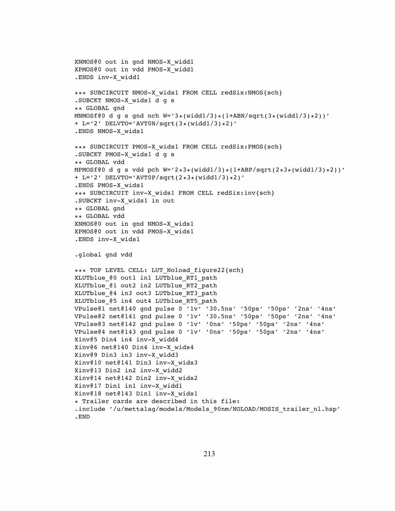
XNMOS@0 out in gnd NMOS-X_widd1XPMOS@0 out in vdd PMOS-X_widd1.ENDS inv-X_widd1
*** SUBCIRCUIT NMOS-X_wids1 FROM CELL redSix:NMOS{sch}.SUBCKT NMOS-X_wids1 d g s** GLOBAL gndMNMOSf@0 d g s gnd nch W=’3*(widd1/3)*(1+ABN/sqrt(3*(widd1/3)*2))’+ L=’2’ DELVTO=’AVT0N/sqrt(3*(widd1/3)*2)’.ENDS NMOS-X_wids1
*** SUBCIRCUIT PMOS-X_wids1 FROM CELL redSix:PMOS{sch}.SUBCKT PMOS-X_wids1 d g s
** GLOBAL vddMPMOSf@0 d g s vdd pch W=’2*3*(widd1/3)*(1+ABP/sqrt(2*3*(widd1/3)*2))’+ L=’2’ DELVTO=’AVT0P/sqrt(2*3*(widd1/3)*2)’.ENDS PMOS-X_wids1*** SUBCIRCUIT inv-X_wids1 FROM CELL redSix:inv{sch}.SUBCKT inv-X_wids1 in out
** GLOBAL gnd** GLOBAL vddXNMOS@0 out in gnd NMOS-X_wids1XPMOS@0 out in vdd PMOS-X_wids1.ENDS inv-X_wids1
.global gnd vdd
*** TOP LEVEL CELL: LUT_Noload_figure22{sch}XLUTblue_@0 out1 in1 LUTblue_RT1_pathXLUTblue_@1 out2 in2 LUTblue_RT2_pathXLUTblue_@4 in3 out3 LUTblue_RT3_pathXLUTblue_@5 in4 out4 LUTblue_RT5_pathVPulse@1 net@140 gnd pulse 0 ’1v’ ’30.5ns’ ’50ps’ ’50ps’ ’2ns’ ’4ns’VPulse@2 net@141 gnd pulse 0 ’1v’ ’30.5ns’ ’50ps’ ’50ps’ ’2ns’ ’4ns’VPulse@3 net@142 gnd pulse 0 ’1v’ ’0ns’ ’50ps’ ’50ps’ ’2ns’ ’4ns’VPulse@4 net@143 gnd pulse 0 ’1v’ ’0ns’ ’50ps’ ’50ps’ ’2ns’ ’4ns’Xinv@5 Din4 in4 inv-X_widd4Xinv@6 net@140 Din4 inv-X_wids4Xinv@9 Din3 in3 inv-X_widd3Xinv@10 net@141 Din3 inv-X_wids3Xinv@13 Din2 in2 inv-X_widd2Xinv@14 net@142 Din2 inv-X_wids2Xinv@17 Din1 in1 inv-X_widd1Xinv@18 net@143 Din1 inv-X_wids1* Trailer cards are described in this file:.include ’/u/mettalag/models/Models_90nm/NOLOAD/MOSIS_trailer_nl.hsp’.END
213

H.2 SPICE Simulation Setup File: HEADERHere is the basic file with default simulation parameters for SPICE. Its extension is‘.hsp’. It contains a pointer to the 90nm CMOS process models for our GasP designs.We use the library with typical (TT) Process, Voltage and Temperature (PVT) settings.
***************************************************************** Header File for Simulation with 90nm MOSIS Transistor Models*****************************************************************
********************************************************************************************************************************.LIB ’/stash/arc/models/tsmc90/hspice/cmn90g_2d5_lk_v1d0.l’ TT
*.LIB ’/stash/arc/models/tsmc90/hspice/cmn90g_1d8_3d3_lk_v1d0.l’ TT
***************************************************************** Options and Parameters****************************************************************.OPTION nomod POST.OPTION SCALE=50n.OPTION CAPTAB.PARAM hdifp=0.PARAM hdifn=0.PARAM ABN=0.PARAM ABP=0.PARAM AVT0P=0.PARAM AVT0N=0.PARAM SUPPLY=1V
***************************************************************** Netlist****************************************************************
214
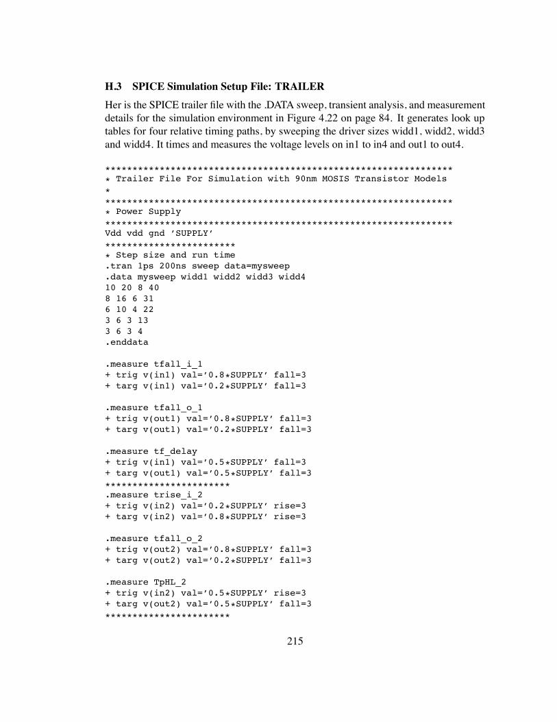
H.3 SPICE Simulation Setup File: TRAILERHer is the SPICE trailer file with the .DATA sweep, transient analysis, and measurementdetails for the simulation environment in Figure 4.22 on page 84. It generates look uptables for four relative timing paths, by sweeping the driver sizes widd1, widd2, widd3and widd4. It times and measures the voltage levels on in1 to in4 and out1 to out4.
***************************************************************** Trailer File For Simulation with 90nm MOSIS Transistor Models
****************************************************************** Power Supply****************************************************************Vdd vdd gnd ’SUPPLY’
************************* Step size and run time.tran 1ps 200ns sweep data=mysweep.data mysweep widd1 widd2 widd3 widd410 20 8 408 16 6 316 10 4 223 6 3 133 6 3 4.enddata
.measure tfall_i_1+ trig v(in1) val=’0.8*SUPPLY’ fall=3+ targ v(in1) val=’0.2*SUPPLY’ fall=3
.measure tfall_o_1+ trig v(out1) val=’0.8*SUPPLY’ fall=3+ targ v(out1) val=’0.2*SUPPLY’ fall=3
.measure tf_delay+ trig v(in1) val=’0.5*SUPPLY’ fall=3+ targ v(out1) val=’0.5*SUPPLY’ fall=3***********************.measure trise_i_2+ trig v(in2) val=’0.2*SUPPLY’ rise=3+ targ v(in2) val=’0.8*SUPPLY’ rise=3
.measure tfall_o_2+ trig v(out2) val=’0.8*SUPPLY’ fall=3+ targ v(out2) val=’0.2*SUPPLY’ fall=3
.measure TpHL_2+ trig v(in2) val=’0.5*SUPPLY’ rise=3+ targ v(out2) val=’0.5*SUPPLY’ fall=3
***********************
215
.measure trise_i_3+ trig v(in3) val=’0.2*SUPPLY’ rise=3+ targ v(in3) val=’0.8*SUPPLY’ rise=3
.measure trise_o_3+ trig v(out3) val=’0.2*SUPPLY’ rise=3+ targ v(out3) val=’0.8*SUPPLY’ rise=3.measure tr_delay_3+ trig v(in3) val=’0.5*SUPPLY’ rise=3+ targ v(out3) val=’0.5*SUPPLY’ rise=3
***********************.measure trise_i_4+ trig v(in4) val=’0.2*SUPPLY’ rise=3+ targ v(in4) val=’0.8*SUPPLY’ rise=3
.measure tfall_o_4+ trig v(out4) val=’0.8*SUPPLY’ fall=3+ targ v(out4) val=’0.2*SUPPLY’ fall=3
.measure TpHL_4+ trig v(in4) val=’0.5*SUPPLY’ rise=3+ targ v(out4) val=’0.5*SUPPLY’ fall=3***********************
216
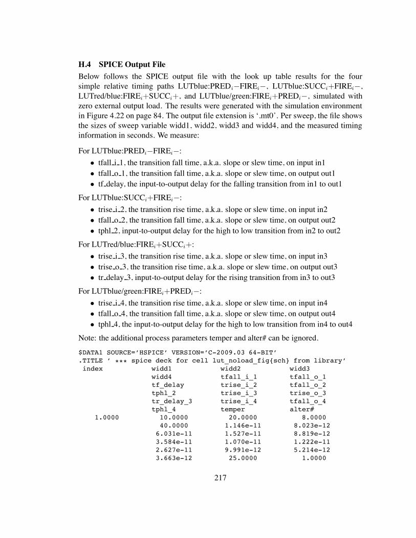
H.4 SPICE Output FileBelow follows the SPICE output file with the look up table results for the foursimple relative timing paths LUTblue:PREDi"FIREi", LUTblue:SUCCi+FIREi",LUTred/blue:FIREi+SUCCi+, and LUTblue/green:FIREi+PREDi", simulated withzero external output load. The results were generated with the simulation environmentin Figure 4.22 on page 84. The output file extension is ‘.mt0’. Per sweep, the file showsthe sizes of sweep variable widd1, widd2, widd3 and widd4, and the measured timinginformation in seconds. We measure:
For LUTblue:PREDi"FIREi":• tfall i 1, the transition fall time, a.k.a. slope or slew time, on input in1• tfall o 1, the transition fall time, a.k.a. slope or slew time, on output out1• tf delay, the input-to-output delay for the falling transition from in1 to out1
For LUTblue:SUCCi+FIREi":• trise i 2, the transition rise time, a.k.a. slope or slew time, on input in2• tfall o 2, the transition fall time, a.k.a. slope or slew time, on output out2• tphl 2, input-to-output delay for the high to low transition from in2 to out2
For LUTred/blue:FIREi+SUCCi+:• trise i 3, the transition rise time, a.k.a. slope or slew time, on input in3• trise o 3, the transition rise time, a.k.a. slope or slew time, on output out3• tr delay 3, input-to-output delay for the rising transition from in3 to out3
For LUTblue/green:FIREi+PREDi":• trise i 4, the transition rise time, a.k.a. slope or slew time, on input in4• tfall o 4, the transition fall time, a.k.a. slope or slew time, on output out4• tphl 4, the input-to-output delay for the high to low transition from in4 to out4
Note: the additional process parameters temper and alter# can be ignored.
$DATA1 SOURCE=’HSPICE’ VERSION=’C-2009.03 64-BIT’.TITLE ’ *** spice deck for cell lut_noload_fig{sch} from library’index widd1 widd2 widd3
widd4 tfall_i_1 tfall_o_1tf_delay trise_i_2 tfall_o_2tphl_2 trise_i_3 trise_o_3tr_delay_3 trise_i_4 tfall_o_4tphl_4 temper alter#
1.0000 10.0000 20.0000 8.000040.0000 1.146e-11 8.023e-12
6.031e-11 1.527e-11 8.819e-123.584e-11 1.070e-11 1.222e-112.627e-11 9.991e-12 5.214e-123.663e-12 25.0000 1.0000
217
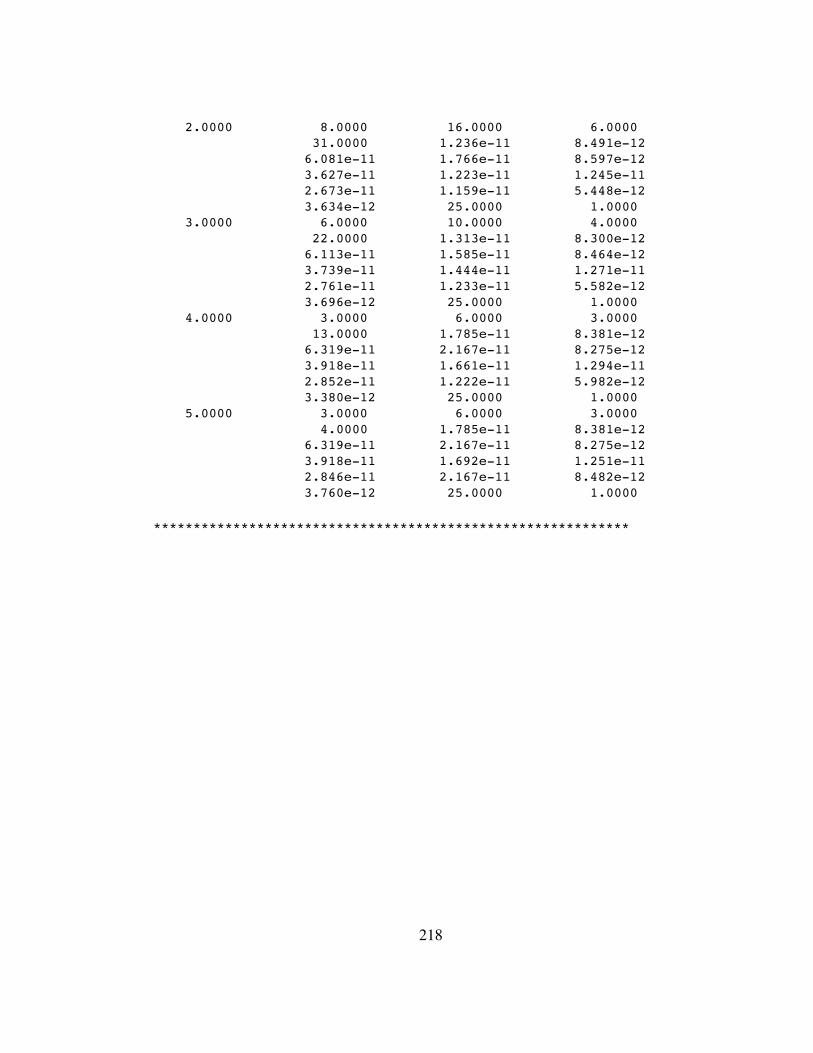
2.0000 8.0000 16.0000 6.000031.0000 1.236e-11 8.491e-12
6.081e-11 1.766e-11 8.597e-123.627e-11 1.223e-11 1.245e-112.673e-11 1.159e-11 5.448e-123.634e-12 25.0000 1.0000
3.0000 6.0000 10.0000 4.000022.0000 1.313e-11 8.300e-12
6.113e-11 1.585e-11 8.464e-123.739e-11 1.444e-11 1.271e-112.761e-11 1.233e-11 5.582e-123.696e-12 25.0000 1.0000
4.0000 3.0000 6.0000 3.000013.0000 1.785e-11 8.381e-12
6.319e-11 2.167e-11 8.275e-123.918e-11 1.661e-11 1.294e-112.852e-11 1.222e-11 5.982e-123.380e-12 25.0000 1.0000
5.0000 3.0000 6.0000 3.00004.0000 1.785e-11 8.381e-12
6.319e-11 2.167e-11 8.275e-123.918e-11 1.692e-11 1.251e-112.846e-11 2.167e-11 8.482e-123.760e-12 25.0000 1.0000
************************************************************
218
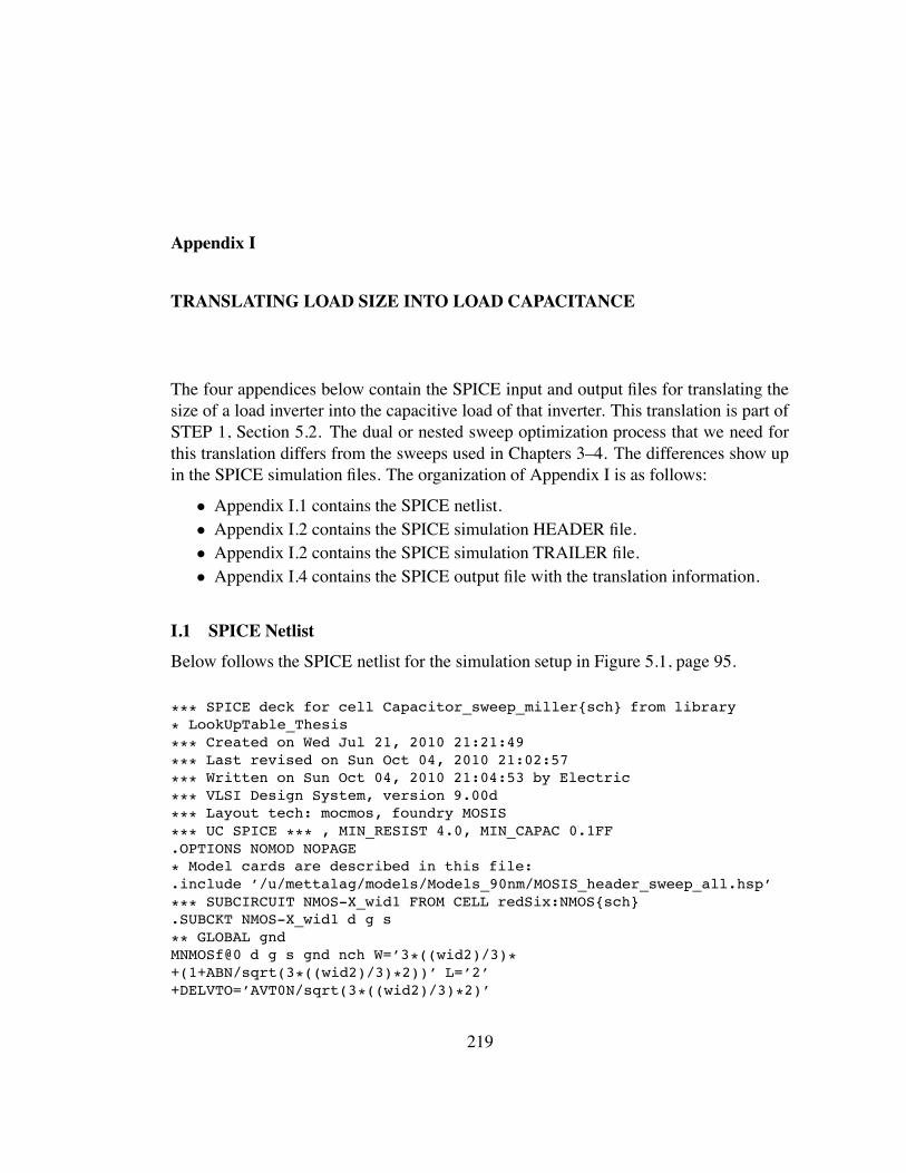
Appendix I
TRANSLATING LOAD SIZE INTO LOAD CAPACITANCE
The four appendices below contain the SPICE input and output files for translating thesize of a load inverter into the capacitive load of that inverter. This translation is part ofSTEP 1, Section 5.2. The dual or nested sweep optimization process that we need forthis translation differs from the sweeps used in Chapters 3–4. The differences show upin the SPICE simulation files. The organization of Appendix I is as follows:
• Appendix I.1 contains the SPICE netlist.• Appendix I.2 contains the SPICE simulation HEADER file.• Appendix I.2 contains the SPICE simulation TRAILER file.• Appendix I.4 contains the SPICE output file with the translation information.
I.1 SPICE Netlist
Below follows the SPICE netlist for the simulation setup in Figure 5.1, page 95.
*** SPICE deck for cell Capacitor_sweep_miller{sch} from library* LookUpTable_Thesis
*** Created on Wed Jul 21, 2010 21:21:49
*** Last revised on Sun Oct 04, 2010 21:02:57*** Written on Sun Oct 04, 2010 21:04:53 by Electric
*** VLSI Design System, version 9.00d*** Layout tech: mocmos, foundry MOSIS
*** UC SPICE *** , MIN_RESIST 4.0, MIN_CAPAC 0.1FF.OPTIONS NOMOD NOPAGE* Model cards are described in this file:.include ’/u/mettalag/models/Models_90nm/MOSIS_header_sweep_all.hsp’
*** SUBCIRCUIT NMOS-X_wid1 FROM CELL redSix:NMOS{sch}.SUBCKT NMOS-X_wid1 d g s
** GLOBAL gndMNMOSf@0 d g s gnd nch W=’3*((wid2)/3)*+(1+ABN/sqrt(3*((wid2)/3)*2))’ L=’2’+DELVTO=’AVT0N/sqrt(3*((wid2)/3)*2)’
219
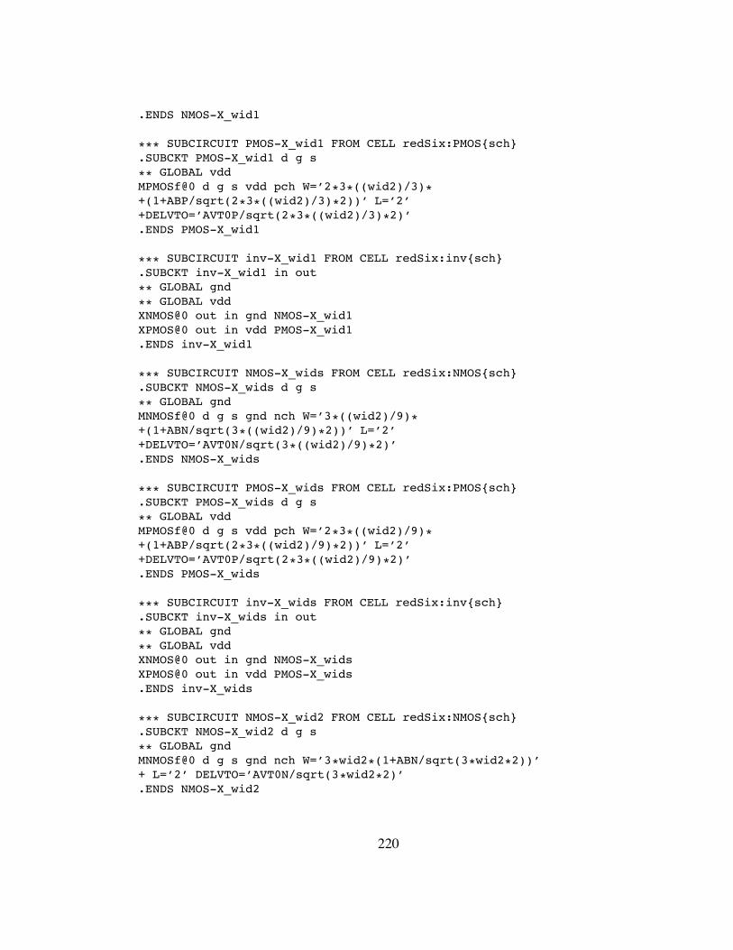
.ENDS NMOS-X_wid1
*** SUBCIRCUIT PMOS-X_wid1 FROM CELL redSix:PMOS{sch}.SUBCKT PMOS-X_wid1 d g s** GLOBAL vddMPMOSf@0 d g s vdd pch W=’2*3*((wid2)/3)*+(1+ABP/sqrt(2*3*((wid2)/3)*2))’ L=’2’+DELVTO=’AVT0P/sqrt(2*3*((wid2)/3)*2)’.ENDS PMOS-X_wid1
*** SUBCIRCUIT inv-X_wid1 FROM CELL redSix:inv{sch}.SUBCKT inv-X_wid1 in out** GLOBAL gnd
** GLOBAL vddXNMOS@0 out in gnd NMOS-X_wid1XPMOS@0 out in vdd PMOS-X_wid1.ENDS inv-X_wid1
*** SUBCIRCUIT NMOS-X_wids FROM CELL redSix:NMOS{sch}.SUBCKT NMOS-X_wids d g s** GLOBAL gndMNMOSf@0 d g s gnd nch W=’3*((wid2)/9)*+(1+ABN/sqrt(3*((wid2)/9)*2))’ L=’2’+DELVTO=’AVT0N/sqrt(3*((wid2)/9)*2)’.ENDS NMOS-X_wids
*** SUBCIRCUIT PMOS-X_wids FROM CELL redSix:PMOS{sch}.SUBCKT PMOS-X_wids d g s** GLOBAL vddMPMOSf@0 d g s vdd pch W=’2*3*((wid2)/9)*+(1+ABP/sqrt(2*3*((wid2)/9)*2))’ L=’2’+DELVTO=’AVT0P/sqrt(2*3*((wid2)/9)*2)’.ENDS PMOS-X_wids
*** SUBCIRCUIT inv-X_wids FROM CELL redSix:inv{sch}.SUBCKT inv-X_wids in out** GLOBAL gnd
** GLOBAL vddXNMOS@0 out in gnd NMOS-X_widsXPMOS@0 out in vdd PMOS-X_wids.ENDS inv-X_wids
*** SUBCIRCUIT NMOS-X_wid2 FROM CELL redSix:NMOS{sch}.SUBCKT NMOS-X_wid2 d g s** GLOBAL gndMNMOSf@0 d g s gnd nch W=’3*wid2*(1+ABN/sqrt(3*wid2*2))’+ L=’2’ DELVTO=’AVT0N/sqrt(3*wid2*2)’.ENDS NMOS-X_wid2
220
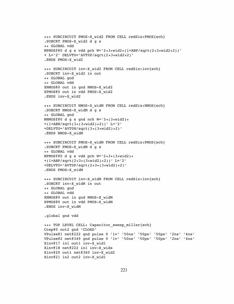
*** SUBCIRCUIT PMOS-X_wid2 FROM CELL redSix:PMOS{sch}.SUBCKT PMOS-X_wid2 d g s
** GLOBAL vddMPMOSf@0 d g s vdd pch W=’2*3*wid2*(1+ABP/sqrt(2*3*wid2*2))’+ L=’2’ DELVTO=’AVT0P/sqrt(2*3*wid2*2)’.ENDS PMOS-X_wid2
*** SUBCIRCUIT inv-X_wid2 FROM CELL redSix:inv{sch}.SUBCKT inv-X_wid2 in out** GLOBAL gnd
** GLOBAL vddXNMOS@0 out in gnd NMOS-X_wid2XPMOS@0 out in vdd PMOS-X_wid2.ENDS inv-X_wid2
*** SUBCIRCUIT NMOS-X_widM FROM CELL redSix:NMOS{sch}.SUBCKT NMOS-X_widM d g s** GLOBAL gndMNMOSf@0 d g s gnd nch W=’3*(3*wid2)*+(1+ABN/sqrt(3*(3*wid2)*2))’ L=’2’+DELVTO=’AVT0N/sqrt(3*(3*wid2)*2)’.ENDS NMOS-X_widM
*** SUBCIRCUIT PMOS-X_widM FROM CELL redSix:PMOS{sch}.SUBCKT PMOS-X_widM d g s** GLOBAL vddMPMOSf@0 d g s vdd pch W=’2*3*(3*wid2)*+(1+ABP/sqrt(2*3*(3*wid2)*2))’ L=’2’+DELVTO=’AVT0P/sqrt(2*3*(3*wid2)*2)’.ENDS PMOS-X_widM
*** SUBCIRCUIT inv-X_widM FROM CELL redSix:inv{sch}.SUBCKT inv-X_widM in out** GLOBAL gnd
** GLOBAL vddXNMOS@0 out in gnd NMOS-X_widMXPMOS@0 out in vdd PMOS-X_widM.ENDS inv-X_widM
.global gnd vdd
*** TOP LEVEL CELL: Capacitor_sweep_miller{sch}Ccap@0 out2 gnd ’CLOAD’VPulse@1 net@222 gnd pulse 0 ’1v’ ’50ns’ ’50ps’ ’50ps’ ’2ns’ ’4ns’VPulse@2 net@349 gnd pulse 0 ’1v’ ’50ns’ ’50ps’ ’50ps’ ’2ns’ ’4ns’Xinv@17 in1 out1 inv-X_wid1Xinv@18 net@222 in1 inv-X_widsXinv@20 out1 net@360 inv-X_wid2Xinv@21 in2 out2 inv-X_wid1
221

Xinv@22 net@349 in2 inv-X_widsXinv@23 net@360 outM inv-X_widM
* Trailer cards are described in this file:.include ’/u/mettalag/models/Models_90nm/MOSIS_trailer_Varcap.hsp’.END
222
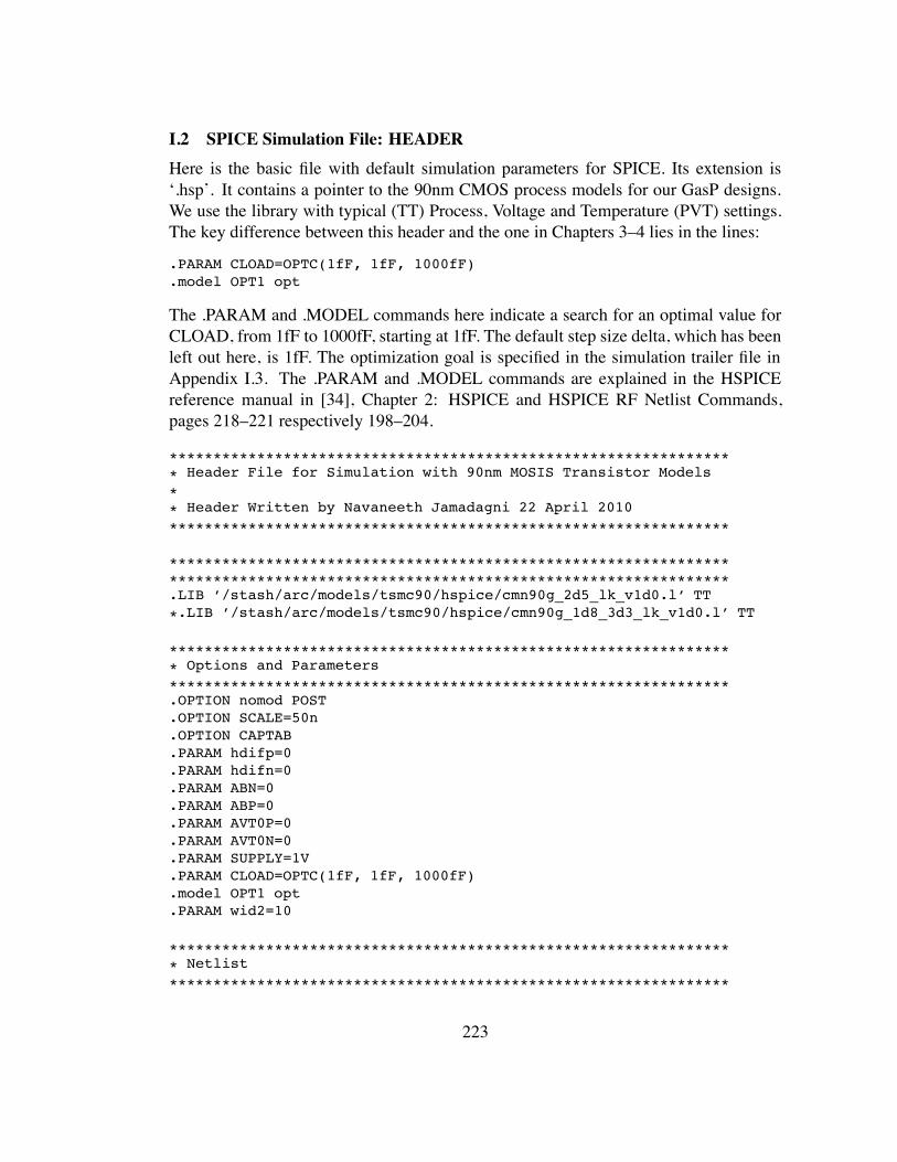
I.2 SPICE Simulation File: HEADERHere is the basic file with default simulation parameters for SPICE. Its extension is‘.hsp’. It contains a pointer to the 90nm CMOS process models for our GasP designs.We use the library with typical (TT) Process, Voltage and Temperature (PVT) settings.The key difference between this header and the one in Chapters 3–4 lies in the lines:
.PARAM CLOAD=OPTC(1fF, 1fF, 1000fF)
.model OPT1 opt
The .PARAM and .MODEL commands here indicate a search for an optimal value forCLOAD, from 1fF to 1000fF, starting at 1fF. The default step size delta, which has beenleft out here, is 1fF. The optimization goal is specified in the simulation trailer file inAppendix I.3. The .PARAM and .MODEL commands are explained in the HSPICEreference manual in [34], Chapter 2: HSPICE and HSPICE RF Netlist Commands,pages 218–221 respectively 198–204.
***************************************************************** Header File for Simulation with 90nm MOSIS Transistor Models** Header Written by Navaneeth Jamadagni 22 April 2010****************************************************************
********************************************************************************************************************************.LIB ’/stash/arc/models/tsmc90/hspice/cmn90g_2d5_lk_v1d0.l’ TT
*.LIB ’/stash/arc/models/tsmc90/hspice/cmn90g_1d8_3d3_lk_v1d0.l’ TT
***************************************************************** Options and Parameters****************************************************************.OPTION nomod POST.OPTION SCALE=50n.OPTION CAPTAB.PARAM hdifp=0.PARAM hdifn=0.PARAM ABN=0.PARAM ABP=0.PARAM AVT0P=0.PARAM AVT0N=0.PARAM SUPPLY=1V.PARAM CLOAD=OPTC(1fF, 1fF, 1000fF).model OPT1 opt.PARAM wid2=10
***************************************************************** Netlist
****************************************************************
223
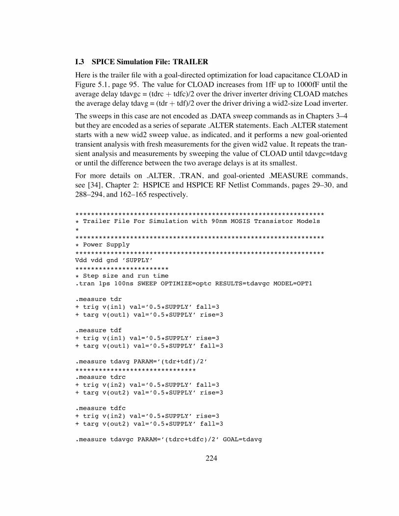
I.3 SPICE Simulation File: TRAILERHere is the trailer file with a goal-directed optimization for load capacitance CLOAD inFigure 5.1, page 95. The value for CLOAD increases from 1fF up to 1000fF until theaverage delay tdavgc = (tdrc + tdfc)/2 over the driver inverter driving CLOAD matchesthe average delay tdavg = (tdr+ tdf)/2 over the driver driving a wid2-size Load inverter.The sweeps in this case are not encoded as .DATA sweep commands as in Chapters 3–4but they are encoded as a series of separate .ALTER statements. Each .ALTER statementstarts with a new wid2 sweep value, as indicated, and it performs a new goal-orientedtransient analysis with fresh measurements for the given wid2 value. It repeats the tran-sient analysis and measurements by sweeping the value of CLOAD until tdavgc=tdavgor until the difference between the two average delays is at its smallest.For more details on .ALTER, .TRAN, and goal-oriented .MEASURE commands,see [34], Chapter 2: HSPICE and HSPICE RF Netlist Commands, pages 29–30, and288–294, and 162–165 respectively.
***************************************************************** Trailer File For Simulation with 90nm MOSIS Transistor Models
****************************************************************** Power Supply
****************************************************************Vdd vdd gnd ’SUPPLY’************************* Step size and run time.tran 1ps 100ns SWEEP OPTIMIZE=optc RESULTS=tdavgc MODEL=OPT1
.measure tdr+ trig v(in1) val=’0.5*SUPPLY’ fall=3+ targ v(out1) val=’0.5*SUPPLY’ rise=3
.measure tdf+ trig v(in1) val=’0.5*SUPPLY’ rise=3+ targ v(out1) val=’0.5*SUPPLY’ fall=3
.measure tdavg PARAM=’(tdr+tdf)/2’*******************************.measure tdrc+ trig v(in2) val=’0.5*SUPPLY’ fall=3+ targ v(out2) val=’0.5*SUPPLY’ rise=3
.measure tdfc+ trig v(in2) val=’0.5*SUPPLY’ rise=3+ targ v(out2) val=’0.5*SUPPLY’ fall=3
.measure tdavgc PARAM=’(tdrc+tdfc)/2’ GOAL=tdavg
224
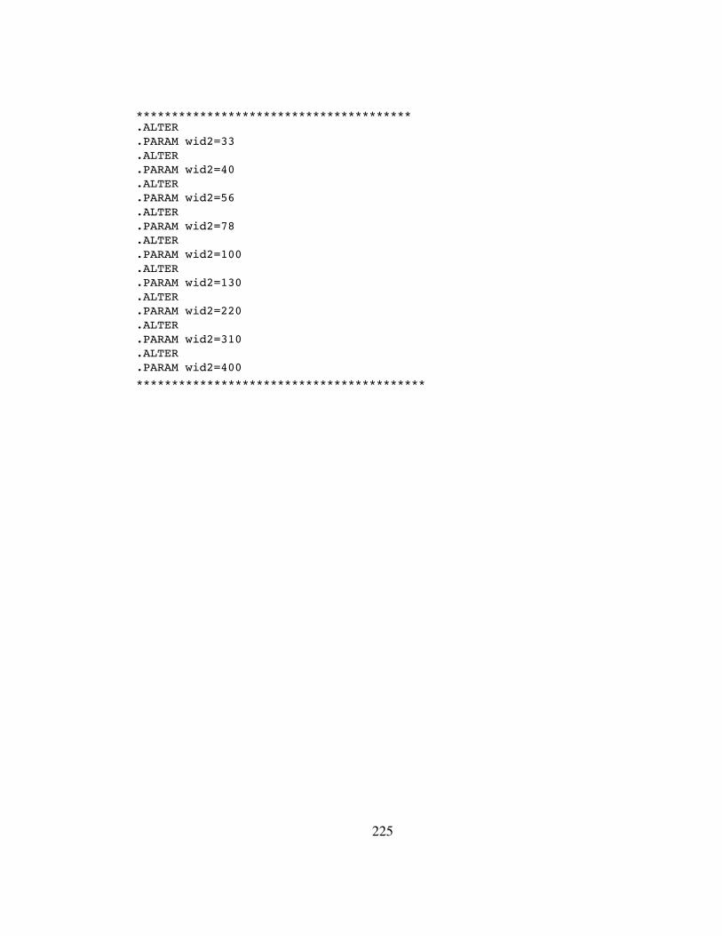
***************************************.ALTER.PARAM wid2=33.ALTER.PARAM wid2=40.ALTER.PARAM wid2=56.ALTER.PARAM wid2=78.ALTER.PARAM wid2=100.ALTER.PARAM wid2=130.ALTER.PARAM wid2=220.ALTER.PARAM wid2=310.ALTER.PARAM wid2=400
*****************************************
225
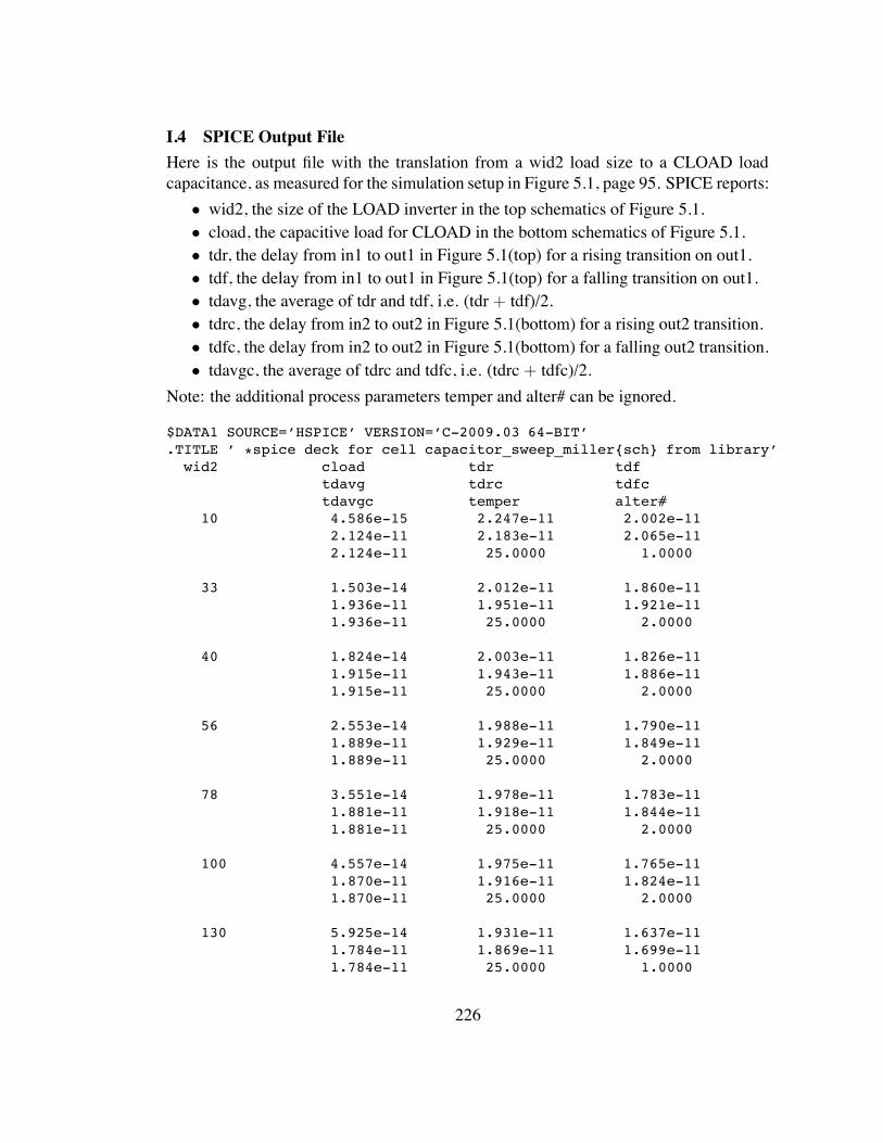
I.4 SPICE Output FileHere is the output file with the translation from a wid2 load size to a CLOAD loadcapacitance, as measured for the simulation setup in Figure 5.1, page 95. SPICE reports:
• wid2, the size of the LOAD inverter in the top schematics of Figure 5.1.• cload, the capacitive load for CLOAD in the bottom schematics of Figure 5.1.• tdr, the delay from in1 to out1 in Figure 5.1(top) for a rising transition on out1.• tdf, the delay from in1 to out1 in Figure 5.1(top) for a falling transition on out1.• tdavg, the average of tdr and tdf, i.e. (tdr + tdf)/2.• tdrc, the delay from in2 to out2 in Figure 5.1(bottom) for a rising out2 transition.• tdfc, the delay from in2 to out2 in Figure 5.1(bottom) for a falling out2 transition.• tdavgc, the average of tdrc and tdfc, i.e. (tdrc + tdfc)/2.
Note: the additional process parameters temper and alter# can be ignored.
$DATA1 SOURCE=’HSPICE’ VERSION=’C-2009.03 64-BIT’.TITLE ’ *spice deck for cell capacitor_sweep_miller{sch} from library’
wid2 cload tdr tdftdavg tdrc tdfctdavgc temper alter#
10 4.586e-15 2.247e-11 2.002e-112.124e-11 2.183e-11 2.065e-112.124e-11 25.0000 1.0000
33 1.503e-14 2.012e-11 1.860e-111.936e-11 1.951e-11 1.921e-111.936e-11 25.0000 2.0000
40 1.824e-14 2.003e-11 1.826e-111.915e-11 1.943e-11 1.886e-111.915e-11 25.0000 2.0000
56 2.553e-14 1.988e-11 1.790e-111.889e-11 1.929e-11 1.849e-111.889e-11 25.0000 2.0000
78 3.551e-14 1.978e-11 1.783e-111.881e-11 1.918e-11 1.844e-111.881e-11 25.0000 2.0000
100 4.557e-14 1.975e-11 1.765e-111.870e-11 1.916e-11 1.824e-111.870e-11 25.0000 2.0000
130 5.925e-14 1.931e-11 1.637e-111.784e-11 1.869e-11 1.699e-111.784e-11 25.0000 1.0000
226
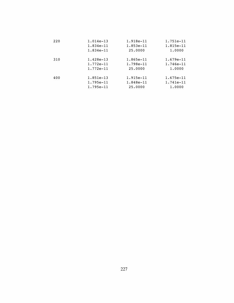
220 1.014e-13 1.918e-11 1.751e-111.834e-11 1.853e-11 1.815e-111.834e-11 25.0000 1.0000
310 1.428e-13 1.865e-11 1.679e-111.772e-11 1.798e-11 1.746e-111.772e-11 25.0000 1.0000
400 1.851e-13 1.915e-11 1.675e-111.795e-11 1.848e-11 1.741e-111.795e-11 25.0000 1.0000
227
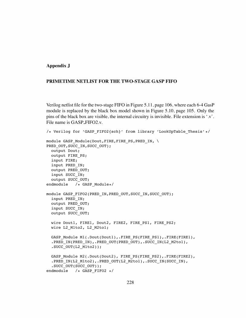
Appendix J
PRIMETIME NETLIST FOR THE TWO-STAGE GASP FIFO
Verilog netlist file for the two-stage FIFO in Figure 5.11, page 106, where each 6-4 GasPmodule is replaced by the black box model shown in Figure 5.10, page 105. Only thepins of the black box are visible, the internal circuitry is invisible. File extension is ‘.v’.File name is GASP FIFO2.v.
/* Verilog for ’GASP_FIFO2{sch}’ from library ’LookUpTable_Thesis’*/
module GASP_Module(Dout,FIRE,FIRE_PS,PRED_IN, \PRED_OUT,SUCC_IN,SUCC_OUT);
output Dout;output FIRE_PS;input FIRE;input PRED_IN;output PRED_OUT;input SUCC_IN;output SUCC_OUT;
endmodule /* GASP_Module*/
module GASP_FIFO2(PRED_IN,PRED_OUT,SUCC_IN,SUCC_OUT);input PRED_IN;output PRED_OUT;input SUCC_IN;output SUCC_OUT;
wire Dout1, FIRE1, Dout2, FIRE2, FIRE_PS1, FIRE_PS2;wire L2_M1to2, L2_M2to1;
GASP_Module M1(.Dout(Dout1),.FIRE_PS(FIRE_PS1),.FIRE(FIRE1),.PRED_IN(PRED_IN),.PRED_OUT(PRED_OUT),.SUCC_IN(L2_M2to1),.SUCC_OUT(L2_M1to2));
GASP_Module M2(.Dout(Dout2), FIRE_PS(FIRE_PS2),.FIRE(FIRE2),.PRED_IN(L2_M1to2),.PRED_OUT(L2_M2to1),.SUCC_IN(SUCC_IN),.SUCC_OUT(SUCC_OUT));
endmodule /* GASP_FIFO2 */
228
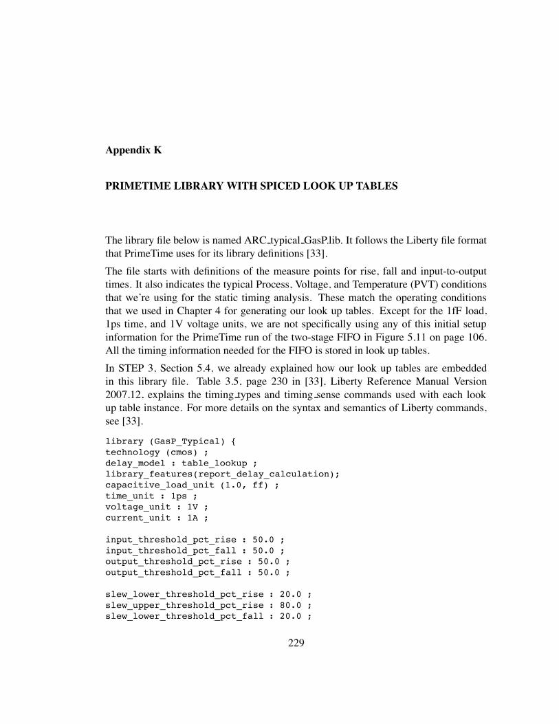
Appendix K
PRIMETIME LIBRARYWITH SPICED LOOK UP TABLES
The library file below is named ARC typical GasP.lib. It follows the Liberty file formatthat PrimeTime uses for its library definitions [33].The file starts with definitions of the measure points for rise, fall and input-to-outputtimes. It also indicates the typical Process, Voltage, and Temperature (PVT) conditionsthat we’re using for the static timing analysis. These match the operating conditionsthat we used in Chapter 4 for generating our look up tables. Except for the 1fF load,1ps time, and 1V voltage units, we are not specifically using any of this initial setupinformation for the PrimeTime run of the two-stage FIFO in Figure 5.11 on page 106.All the timing information needed for the FIFO is stored in look up tables.In STEP 3, Section 5.4, we already explained how our look up tables are embeddedin this library file. Table 3.5, page 230 in [33], Liberty Reference Manual Version2007.12, explains the timing types and timing sense commands used with each lookup table instance. For more details on the syntax and semantics of Liberty commands,see [33].
library (GasP_Typical) {technology (cmos) ;delay_model : table_lookup ;library_features(report_delay_calculation);capacitive_load_unit (1.0, ff) ;time_unit : 1ps ;voltage_unit : 1V ;current_unit : 1A ;
input_threshold_pct_rise : 50.0 ;input_threshold_pct_fall : 50.0 ;output_threshold_pct_rise : 50.0 ;output_threshold_pct_fall : 50.0 ;
slew_lower_threshold_pct_rise : 20.0 ;slew_upper_threshold_pct_rise : 80.0 ;slew_lower_threshold_pct_fall : 20.0 ;
229
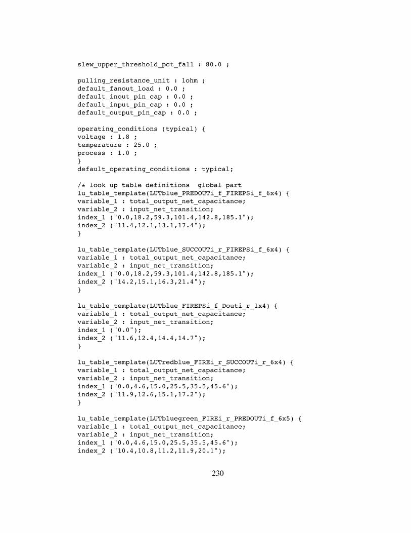
slew_upper_threshold_pct_fall : 80.0 ;
pulling_resistance_unit : 1ohm ;default_fanout_load : 0.0 ;default_inout_pin_cap : 0.0 ;default_input_pin_cap : 0.0 ;default_output_pin_cap : 0.0 ;
operating_conditions (typical) {voltage : 1.8 ;temperature : 25.0 ;process : 1.0 ;}default_operating_conditions : typical;
/* look up table definitions global partlu_table_template(LUTblue_PREDOUTi_f_FIREPSi_f_6x4) {variable_1 : total_output_net_capacitance;variable_2 : input_net_transition;index_1 ("0.0,18.2,59.3,101.4,142.8,185.1");index_2 ("11.4,12.1,13.1,17.4");}
lu_table_template(LUTblue_SUCCOUTi_r_FIREPSi_f_6x4) {variable_1 : total_output_net_capacitance;variable_2 : input_net_transition;index_1 ("0.0,18.2,59.3,101.4,142.8,185.1");index_2 ("14.2,15.1,16.3,21.4");}
lu_table_template(LUTblue_FIREPSi_f_Douti_r_1x4) {variable_1 : total_output_net_capacitance;variable_2 : input_net_transition;index_1 ("0.0");index_2 ("11.6,12.4,14.4,14.7");}
lu_table_template(LUTredblue_FIREi_r_SUCCOUTi_r_6x4) {variable_1 : total_output_net_capacitance;variable_2 : input_net_transition;index_1 ("0.0,4.6,15.0,25.5,35.5,45.6");index_2 ("11.9,12.6,15.1,17.2");}
lu_table_template(LUTbluegreen_FIREi_r_PREDOUTi_f_6x5) {variable_1 : total_output_net_capacitance;variable_2 : input_net_transition;index_1 ("0.0,4.6,15.0,25.5,35.5,45.6");index_2 ("10.4,10.8,11.2,11.9,20.1");
230
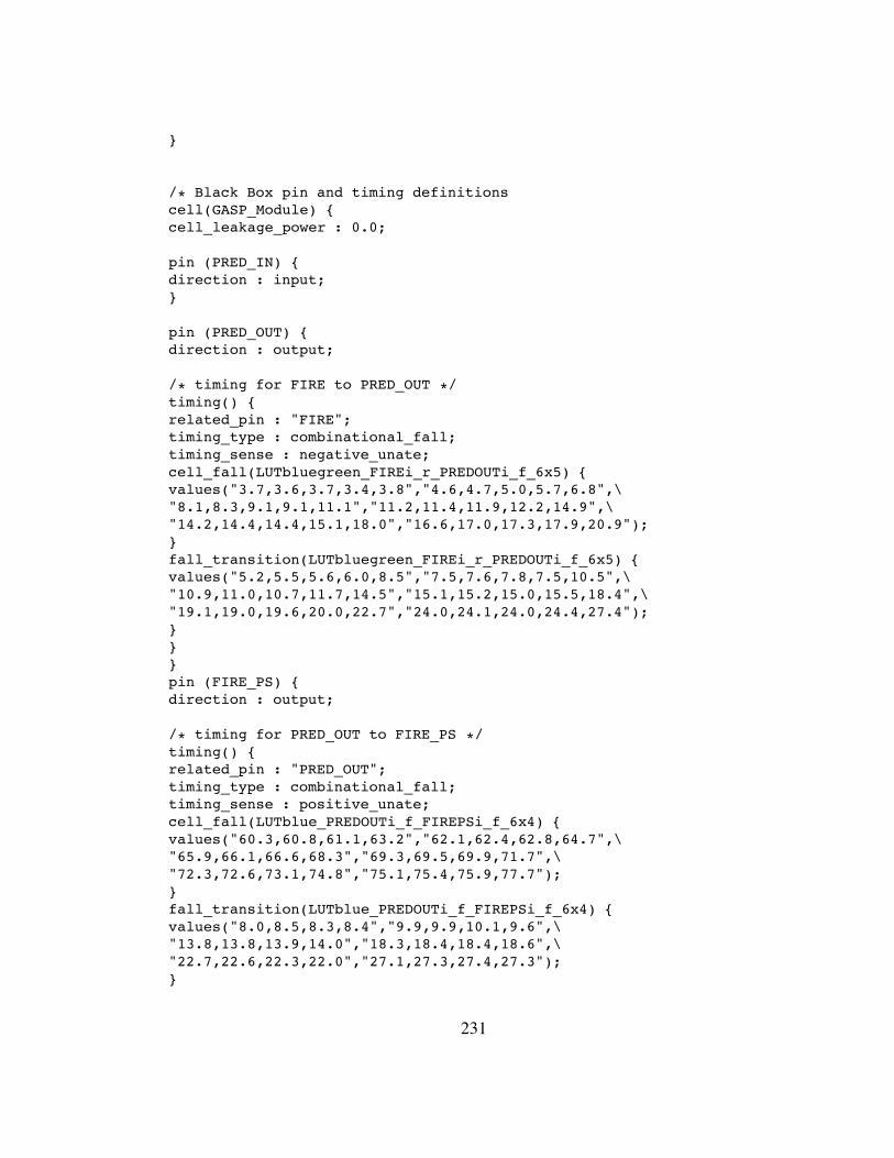
}
/* Black Box pin and timing definitionscell(GASP_Module) {cell_leakage_power : 0.0;
pin (PRED_IN) {direction : input;}
pin (PRED_OUT) {direction : output;
/* timing for FIRE to PRED_OUT */timing() {related_pin : "FIRE";timing_type : combinational_fall;timing_sense : negative_unate;cell_fall(LUTbluegreen_FIREi_r_PREDOUTi_f_6x5) {values("3.7,3.6,3.7,3.4,3.8","4.6,4.7,5.0,5.7,6.8",\"8.1,8.3,9.1,9.1,11.1","11.2,11.4,11.9,12.2,14.9",\"14.2,14.4,14.4,15.1,18.0","16.6,17.0,17.3,17.9,20.9");}fall_transition(LUTbluegreen_FIREi_r_PREDOUTi_f_6x5) {values("5.2,5.5,5.6,6.0,8.5","7.5,7.6,7.8,7.5,10.5",\"10.9,11.0,10.7,11.7,14.5","15.1,15.2,15.0,15.5,18.4",\"19.1,19.0,19.6,20.0,22.7","24.0,24.1,24.0,24.4,27.4");}}}pin (FIRE_PS) {direction : output;
/* timing for PRED_OUT to FIRE_PS */timing() {related_pin : "PRED_OUT";timing_type : combinational_fall;timing_sense : positive_unate;cell_fall(LUTblue_PREDOUTi_f_FIREPSi_f_6x4) {values("60.3,60.8,61.1,63.2","62.1,62.4,62.8,64.7",\"65.9,66.1,66.6,68.3","69.3,69.5,69.9,71.7",\"72.3,72.6,73.1,74.8","75.1,75.4,75.9,77.7");}fall_transition(LUTblue_PREDOUTi_f_FIREPSi_f_6x4) {values("8.0,8.5,8.3,8.4","9.9,9.9,10.1,9.6",\"13.8,13.8,13.9,14.0","18.3,18.4,18.4,18.6",\"22.7,22.6,22.3,22.0","27.1,27.3,27.4,27.3");}
231
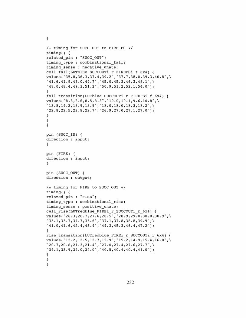
}
/* timing for SUCC_OUT to FIRE_PS */timing() {related_pin : "SUCC_OUT";timing_type : combinational_fall;timing_sense : negative_unate;cell_fall(LUTblue_SUCCOUTi_r_FIREPSi_f_6x4) {values("35.8,36.3,37.4,39.2","37.7,38.0,39.3,40.8",\"41.6,41.9,43.0,44.7","45.0,45.3,46.3,48.1",\"48.0,48.4,49.3,51.2","50.9,51.2,52.1,54.0");}fall_transition(LUTblue_SUCCOUTi_r_FIREPSi_f_6x4) {values("8.8,8.6,8.5,8.3","10.0,10.1,9.6,10.8",\"13.8,14.2,13.9,13.9","18.0,18.0,18.3,18.2",\"22.8,22.5,22.8,22.7","26.9,27.0,27.1,27.0");}}}
pin (SUCC_IN) {direction : input;}
pin (FIRE) {direction : input;}
pin (SUCC_OUT) {direction : output;
/* timing for FIRE to SUCC_OUT */timing() {related_pin : "FIRE";timing_type : combinational_rise;timing_sense : positive_unate;cell_rise(LUTredblue_FIREi_r_SUCCOUTi_r_6x4) {values("26.3,26.7,27.6,28.5","28.9,29.0,30.0,30.9",\"33.1,33.7,34.7,35.6","37.1,37.8,38.8,39.9",\"41.0,41.6,42.4,43.4","44.3,45.3,46.4,47.2");}rise_transition(LUTredblue_FIREi_r_SUCCOUTi_r_6x4) {values("12.2,12.5,12.7,12.9","15.2,14.9,15.4,16.0",\"20.7,20.8,21.3,21.4","27.0,27.4,27.6,27.7",\"34.1,33.9,34.0,34.0","40.5,40.4,40.4,41.0");}}}
232
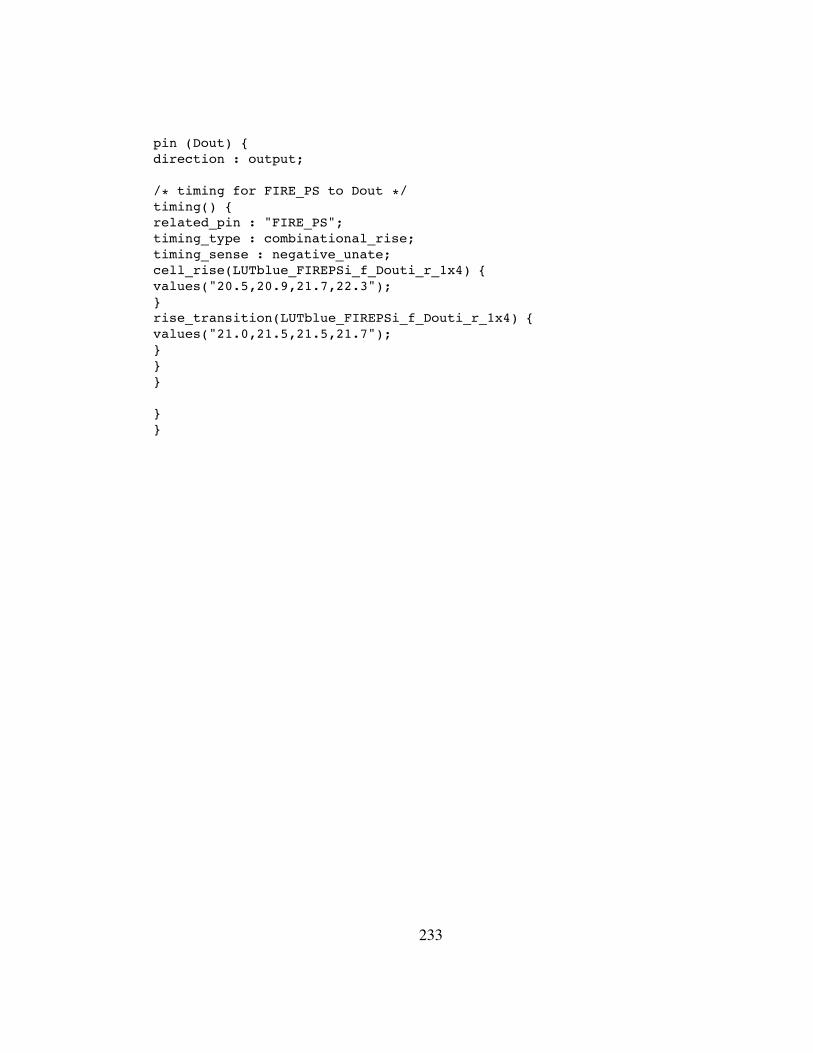
pin (Dout) {direction : output;
/* timing for FIRE_PS to Dout */timing() {related_pin : "FIRE_PS";timing_type : combinational_rise;timing_sense : negative_unate;cell_rise(LUTblue_FIREPSi_f_Douti_r_1x4) {values("20.5,20.9,21.7,22.3");}rise_transition(LUTblue_FIREPSi_f_Douti_r_1x4) {values("21.0,21.5,21.5,21.7");}}}
}}
233
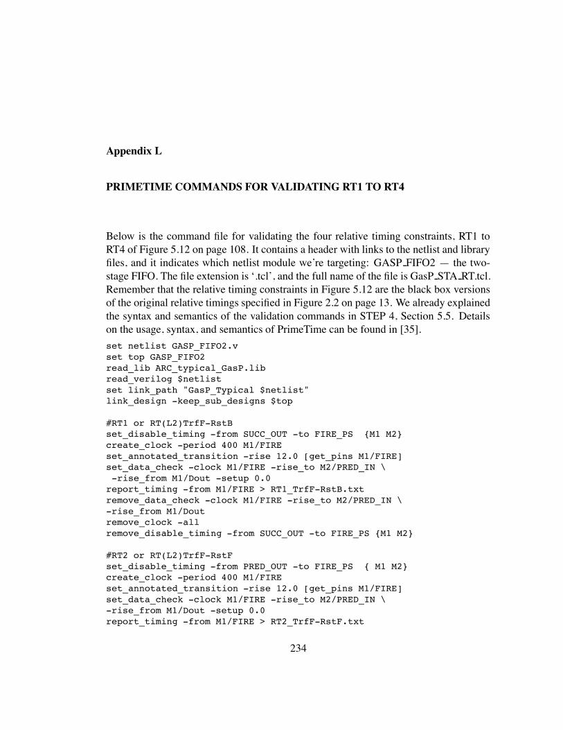
Appendix L
PRIMETIME COMMANDS FOR VALIDATING RT1 TO RT4
Below is the command file for validating the four relative timing constraints, RT1 toRT4 of Figure 5.12 on page 108. It contains a header with links to the netlist and libraryfiles, and it indicates which netlist module we’re targeting: GASP FIFO2 — the two-stage FIFO. The file extension is ‘.tcl’, and the full name of the file is GasP STA RT.tcl.Remember that the relative timing constraints in Figure 5.12 are the black box versionsof the original relative timings specified in Figure 2.2 on page 13. We already explainedthe syntax and semantics of the validation commands in STEP 4, Section 5.5. Detailson the usage, syntax, and semantics of PrimeTime can be found in [35].set netlist GASP_FIFO2.vset top GASP_FIFO2read_lib ARC_typical_GasP.libread_verilog $netlistset link_path "GasP_Typical $netlist"link_design -keep_sub_designs $top
#RT1 or RT(L2)TrfF-RstBset_disable_timing -from SUCC_OUT -to FIRE_PS {M1 M2}create_clock -period 400 M1/FIREset_annotated_transition -rise 12.0 [get_pins M1/FIRE]set_data_check -clock M1/FIRE -rise_to M2/PRED_IN \-rise_from M1/Dout -setup 0.0
report_timing -from M1/FIRE > RT1_TrfF-RstB.txtremove_data_check -clock M1/FIRE -rise_to M2/PRED_IN \-rise_from M1/Doutremove_clock -allremove_disable_timing -from SUCC_OUT -to FIRE_PS {M1 M2}
#RT2 or RT(L2)TrfF-RstFset_disable_timing -from PRED_OUT -to FIRE_PS { M1 M2}create_clock -period 400 M1/FIREset_annotated_transition -rise 12.0 [get_pins M1/FIRE]set_data_check -clock M1/FIRE -rise_to M2/PRED_IN \-rise_from M1/Dout -setup 0.0report_timing -from M1/FIRE > RT2_TrfF-RstF.txt
234
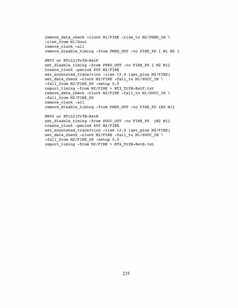
remove_data_check -clock M1/FIRE -rise_to M2/PRED_IN \-rise_from M1/Doutremove_clock -allremove_disable_timing -from PRED_OUT -to FIRE_PS { M1 M2 }
#RT3 or RT(L2)TrfB-RstFset_disable_timing -from PRED_OUT -to FIRE_PS { M2 M1}create_clock -period 400 M2/FIREset_annotated_transition -rise 12.0 [get_pins M2/FIRE]set_data_check -clock M2/FIRE -fall_to M1/SUCC_IN \-fall_from M2/FIRE_PS -setup 0.0report_timing -from M2/FIRE > RT3_TrfB-RstF.txtremove_data_check -clock M2/FIRE -fall_to M1/SUCC_IN \-fall_from M2/FIRE_PSremove_clock -allremove_disable_timing -from PRED_OUT -to FIRE_PS {M2 M1}
#RT4 or RT(L2)TrfB-RstBset_disable_timing -from SUCC_OUT -to FIRE_PS {M2 M1}create_clock -period 400 M2/FIREset_annotated_transition -rise 12.0 [get_pins M2/FIRE]set_data_check -clock M2/FIRE -fall_to M1/SUCC_IN \-fall_from M2/FIRE_PS -setup 0.0report_timing -from M2/FIRE > RT4_TrfB-RstB.txt
235
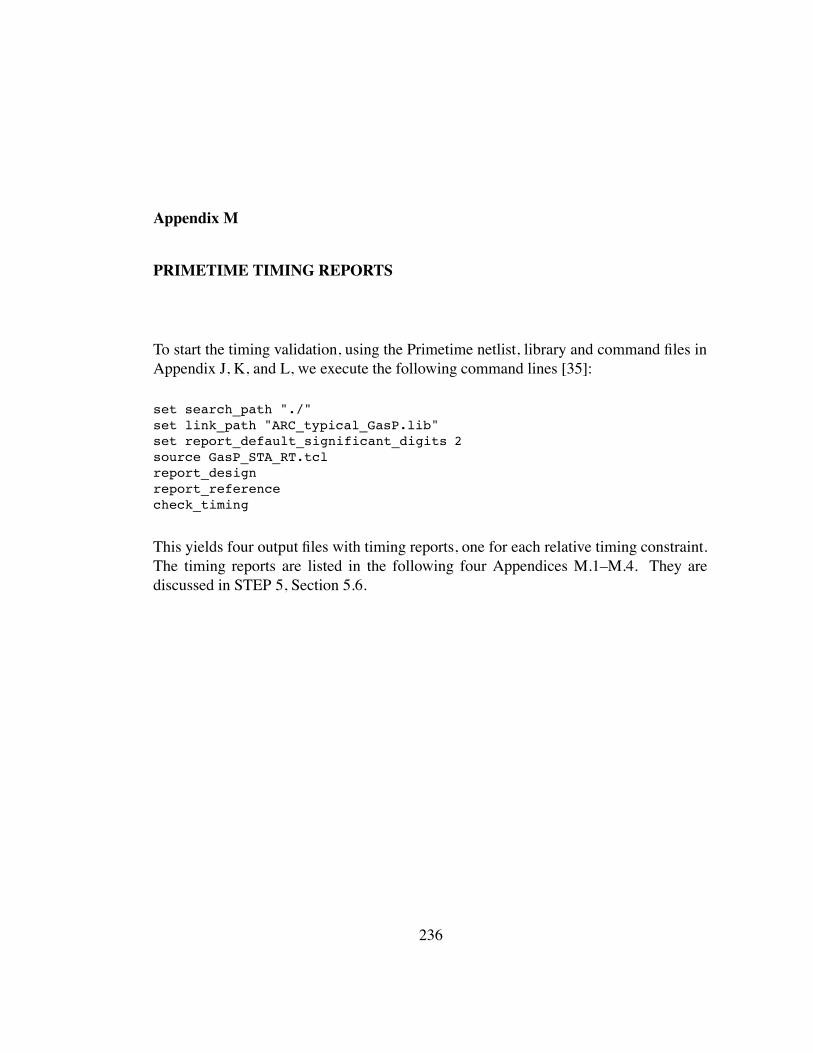
Appendix M
PRIMETIME TIMING REPORTS
To start the timing validation, using the Primetime netlist, library and command files inAppendix J, K, and L, we execute the following command lines [35]:
set search_path "./"set link_path "ARC_typical_GasP.lib"set report_default_significant_digits 2source GasP_STA_RT.tclreport_designreport_referencecheck_timing
This yields four output files with timing reports, one for each relative timing constraint.The timing reports are listed in the following four Appendices M.1–M.4. They arediscussed in STEP 5, Section 5.6.
236
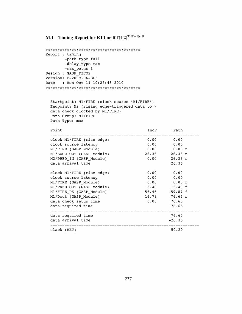
M.1 Timing Report for RT1 or RT(L2)TrfF!RstB
****************************************Report : timing
-path_type full-delay_type max-max_paths 1
Design : GASP_FIFO2Version: C-2009.06-SP3Date : Mon Oct 11 10:28:45 2010
****************************************
Startpoint: M1/FIRE (clock source ’M1/FIRE’)Endpoint: M2 (rising edge-triggered data to \data check clocked by M1/FIRE)Path Group: M1/FIREPath Type: max
Point Incr Path---------------------------------------------------------------clock M1/FIRE (rise edge) 0.00 0.00clock source latency 0.00 0.00M1/FIRE (GASP_Module) 0.00 0.00 rM1/SUCC_OUT (GASP_Module) 26.36 26.36 rM2/PRED_IN (GASP_Module) 0.00 26.36 rdata arrival time 26.36
clock M1/FIRE (rise edge) 0.00 0.00clock source latency 0.00 0.00M1/FIRE (GASP_Module) 0.00 0.00 rM1/PRED_OUT (GASP_Module) 3.40 3.40 fM1/FIRE_PS (GASP_Module) 56.46 59.87 fM1/Dout (GASP_Module) 16.78 76.65 rdata check setup time 0.00 76.65data required time 76.65---------------------------------------------------------------data required time 76.65data arrival time -26.36---------------------------------------------------------------slack (MET) 50.29
237

M.2 Timing Report for RT2 or RT(L2)TrfF!RstF
****************************************Report : timing
-path_type full-delay_type max-max_paths 1
Design : GASP_FIFO2Version: C-2009.06-SP3Date : Mon Oct 11 10:28:45 2010
****************************************
Startpoint: M1/FIRE (clock source ’M1/FIRE’)Endpoint: M2 (rising edge-triggered data to data \check clocked by M1/FIRE)Path Group: M1/FIREPath Type: max
Point Incr Path---------------------------------------------------------------clock M1/FIRE (rise edge) 0.00 0.00clock source latency 0.00 0.00M1/FIRE (GASP_Module) 0.00 0.00 rM1/SUCC_OUT (GASP_Module) 26.36 26.36 rM2/PRED_IN (GASP_Module) 0.00 26.36 rdata arrival time 26.36
clock M1/FIRE (rise edge) 0.00 0.00clock source latency 0.00 0.00M1/FIRE (GASP_Module) 0.00 0.00 rM1/SUCC_OUT (GASP_Module) 26.36 26.36 rM1/FIRE_PS (GASP_Module) 34.71 61.07 fM1/Dout (GASP_Module) 19.32 80.39 rdata check setup time 0.00 80.39data required time 80.39---------------------------------------------------------------data required time 80.39data arrival time -26.36---------------------------------------------------------------slack (MET) 54.03
238
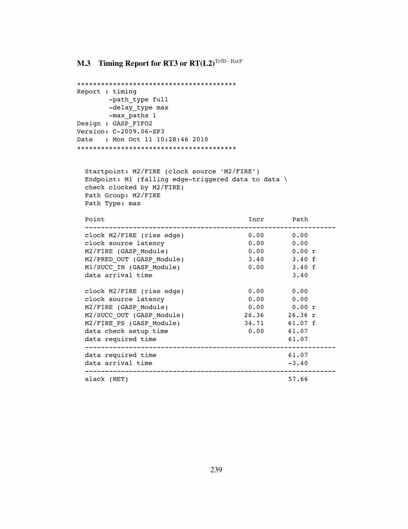
M.3 Timing Report for RT3 or RT(L2)TrfB!RstF
****************************************Report : timing
-path_type full-delay_type max-max_paths 1
Design : GASP_FIFO2Version: C-2009.06-SP3Date : Mon Oct 11 10:28:46 2010
****************************************
Startpoint: M2/FIRE (clock source ’M2/FIRE’)Endpoint: M1 (falling edge-triggered data to data \check clocked by M2/FIRE)Path Group: M2/FIREPath Type: max
Point Incr Path---------------------------------------------------------------clock M2/FIRE (rise edge) 0.00 0.00clock source latency 0.00 0.00M2/FIRE (GASP_Module) 0.00 0.00 rM2/PRED_OUT (GASP_Module) 3.40 3.40 fM1/SUCC_IN (GASP_Module) 0.00 3.40 fdata arrival time 3.40
clock M2/FIRE (rise edge) 0.00 0.00clock source latency 0.00 0.00M2/FIRE (GASP_Module) 0.00 0.00 rM2/SUCC_OUT (GASP_Module) 26.36 26.36 rM2/FIRE_PS (GASP_Module) 34.71 61.07 fdata check setup time 0.00 61.07data required time 61.07---------------------------------------------------------------data required time 61.07data arrival time -3.40---------------------------------------------------------------slack (MET) 57.66
239
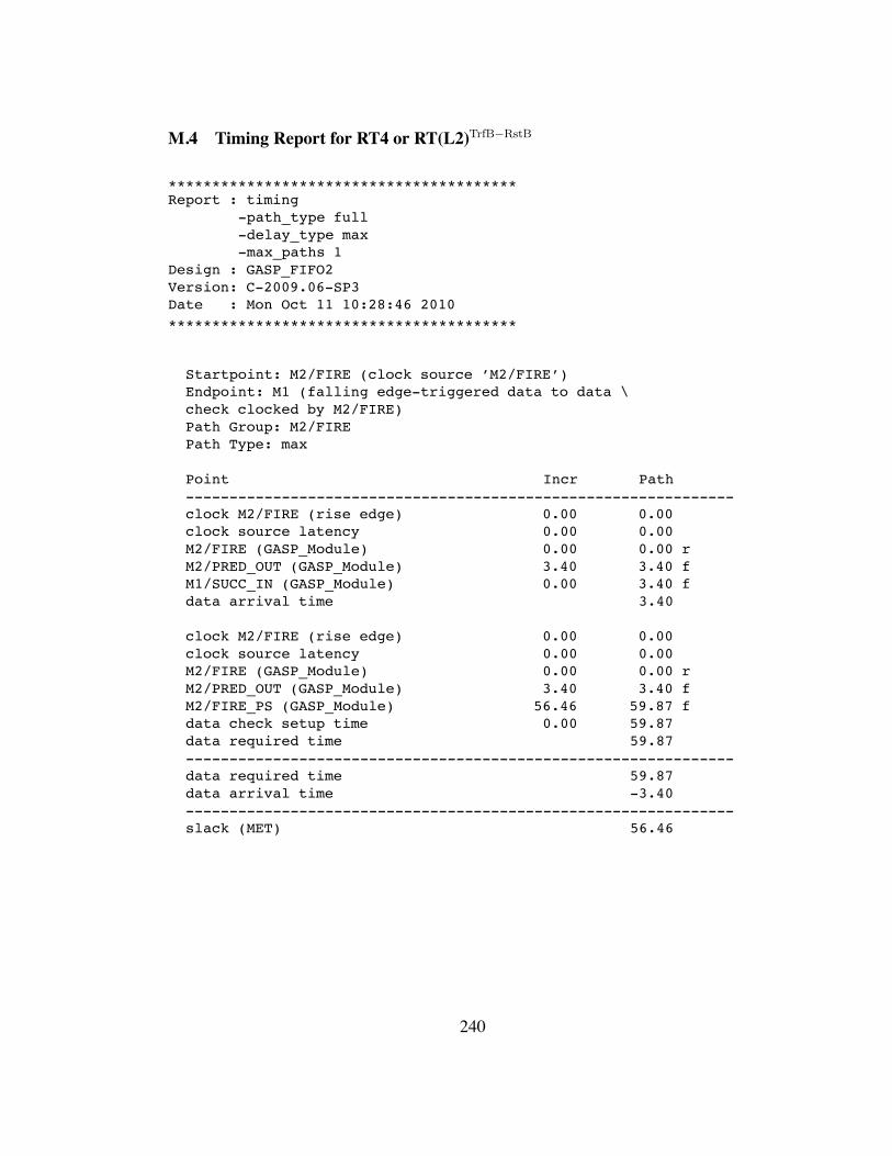
M.4 Timing Report for RT4 or RT(L2)TrfB!RstB
****************************************Report : timing
-path_type full-delay_type max-max_paths 1
Design : GASP_FIFO2Version: C-2009.06-SP3Date : Mon Oct 11 10:28:46 2010
****************************************
Startpoint: M2/FIRE (clock source ’M2/FIRE’)Endpoint: M1 (falling edge-triggered data to data \check clocked by M2/FIRE)Path Group: M2/FIREPath Type: max
Point Incr Path---------------------------------------------------------------clock M2/FIRE (rise edge) 0.00 0.00clock source latency 0.00 0.00M2/FIRE (GASP_Module) 0.00 0.00 rM2/PRED_OUT (GASP_Module) 3.40 3.40 fM1/SUCC_IN (GASP_Module) 0.00 3.40 fdata arrival time 3.40
clock M2/FIRE (rise edge) 0.00 0.00clock source latency 0.00 0.00M2/FIRE (GASP_Module) 0.00 0.00 rM2/PRED_OUT (GASP_Module) 3.40 3.40 fM2/FIRE_PS (GASP_Module) 56.46 59.87 fdata check setup time 0.00 59.87data required time 59.87---------------------------------------------------------------data required time 59.87data arrival time -3.40---------------------------------------------------------------slack (MET) 56.46
240
Appendix N
BONUS MATERIAL: DISTANCE CONSTRAINT GRAPH
Reprinted with permission from the Asynchronous Research Center (ARC) at PortlandState University, this internal ARC report can be found in the thesis reference list asreference [15]. The full citation is as follows:
• Swetha Mettala Gilla. Distance Constraint Graph: A Graphical Representation for6-4 GasP showing how Relative Timings constrain the Module Distances. Tech-nical Report, ARC2009-smg01, Asynchronous Research Center, Portland StateUniversity, September, 2009.
241
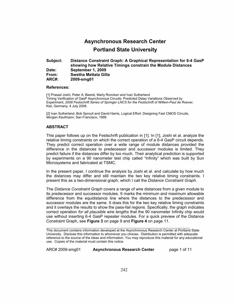
_____________________________________________________________________________ This document contains information developed at the Asynchronous Research Center at Portland State University. Disclose this information to whomever you choose. Distribution is permitted with adequate reference to the source of the ideas and information. You may reproduce this material for any educational use. Copies of the material must contain this notice.
ARC# 2009-smg01 Asynchronous Research Center page 1 of 11
Asynchronous Research Center
Portland State University Subject: Distance Constraint Graph: A Graphical Representation for 6-4 GasP
showing how Relative Timings constrain the Module Distances Date: September 1, 2009 From: Swetha Mettala Gilla ARC#: 2009-smg01
References:
[1] Prasad Joshi, Peter A; Beerel, Marly Roncken and Ivan Sutherland Timing Verification of GasP Asynchronous Circuits: Predicted Delay Variations Observed by Experiment, 2008 Festschrift Series of Springer LNCS for the Festschrift of Willem-Paul de Roever, Kiel, Germany, 4 July 2008. [2] Ivan Sutherland, Bob Sproull and David Harris, Logical Effort: Designing Fast CMOS Circuits, Morgan Kaufmann, San Francisco, 1999
ABSTRACT
This paper follows up on the Festschrift publication in [1]. In [1], Joshi et al. analyze the relative timing constraints on which the correct operation of a 6-4 GasP circuit depends. They predict correct operation over a wide range of module distances provided the difference in the distances to predecessor and successor modules is limited. They predict failure if the distances differ by too much. Their analytical prediction is supported by experiments on a 90 nanometer test chip called ―Infinity‖ which was built by Sun Microsystems and fabricated at TSMC.
In the present paper, I continue the analysis by Joshi et al. and calculate by how much the distances may differ and still maintain the two key relative timing constraints. I present this as a two-dimensional graph, which I call the Distance Constraint Graph.
The Distance Constraint Graph covers a range of wire distances from a given module to its predecessor and successor modules. It marks the minimum and maximum allowable difference from the equidistance line where the distances to the predecessor and successor modules are the same. It does this for the two key relative timing constraints and it overlays the results to show the pass-fail regions. Specifically, the graph indicates correct operation for all plausible wire lengths that the 90 nanometer Infinity chip would use without inserting 6-4 GasP repeater modules. For a quick preview of the Distance Constraint Graph, see Figure 3 on page 9 and Figure 4 on page 11.
242
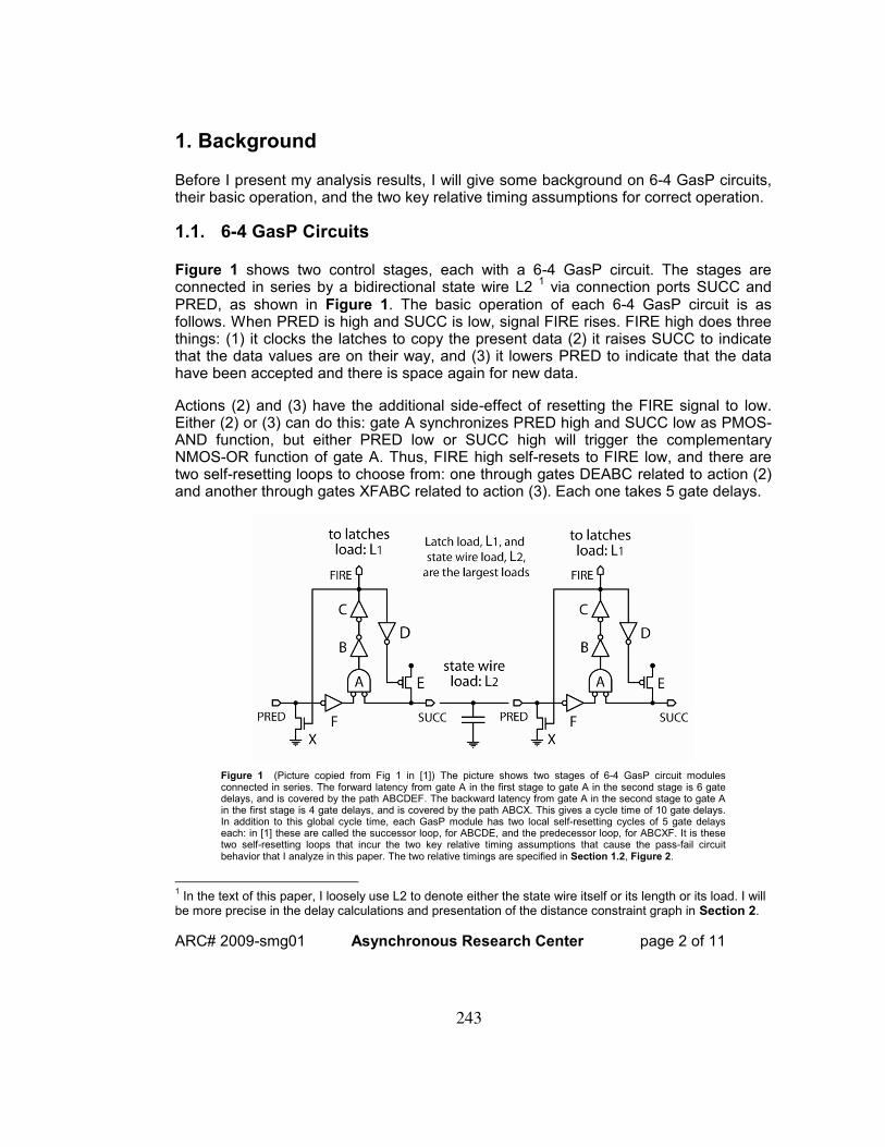
ARC# 2009-smg01 Asynchronous Research Center page 2 of 11
1. Background
Before I present my analysis results, I will give some background on 6-4 GasP circuits, their basic operation, and the two key relative timing assumptions for correct operation.
1.1. 6-4 GasP Circuits
Figure 1 shows two control stages, each with a 6-4 GasP circuit. The stages are connected in series by a bidirectional state wire L2
1 via connection ports SUCC and
PRED, as shown in Figure 1. The basic operation of each 6-4 GasP circuit is as follows. When PRED is high and SUCC is low, signal FIRE rises. FIRE high does three things: (1) it clocks the latches to copy the present data (2) it raises SUCC to indicate that the data values are on their way, and (3) it lowers PRED to indicate that the data have been accepted and there is space again for new data.
Actions (2) and (3) have the additional side-effect of resetting the FIRE signal to low. Either (2) or (3) can do this: gate A synchronizes PRED high and SUCC low as PMOS-AND function, but either PRED low or SUCC high will trigger the complementary NMOS-OR function of gate A. Thus, FIRE high self-resets to FIRE low, and there are two self-resetting loops to choose from: one through gates DEABC related to action (2) and another through gates XFABC related to action (3). Each one takes 5 gate delays.
Figure 1 (Picture copied from Fig 1 in [1]) The picture shows two stages of 6-4 GasP circuit modules connected in series. The forward latency from gate A in the first stage to gate A in the second stage is 6 gate delays, and is covered by the path ABCDEF. The backward latency from gate A in the second stage to gate A in the first stage is 4 gate delays, and is covered by the path ABCX. This gives a cycle time of 10 gate delays. In addition to this global cycle time, each GasP module has two local self-resetting cycles of 5 gate delays each: in [1] these are called the successor loop, for ABCDE, and the predecessor loop, for ABCXF. It is these two self-resetting loops that incur the two key relative timing assumptions that cause the pass-fail circuit behavior that I analyze in this paper. The two relative timings are specified in Section 1.2, Figure 2.
1 In the text of this paper, I loosely use L2 to denote either the state wire itself or its length or its load. I will
be more precise in the delay calculations and presentation of the distance constraint graph in Section 2.
243
ARC# 2009-smg01 Asynchronous Research Center page 3 of 11
In 6-4 GasP, one can count delay in terms of logic gate delays, because the modules are custom-designed using Logical Effort [2]. This means that the transistors in each logic gate are sized such that all logic gates have the same delay. Gate sizing takes into account the transistor sizes of the gates that it drives and the connecting wire lengths.
This works as long as one can adequately predict the wire lengths. Gates A, B, D, F in Figure 1 each drive a single local gate, and so one may assume that the connecting wire lengths are known in advance. The situation for gate C is more complicated: C drives two local gates, D and X, and a number of latches with a total latch load of L1, as well as a not so local wire between the gates and the latches. Fortunately, it is possible to place the latches near the 6-4 GasP controller, and design a macro module that contains both the data and the control and connects these with a fixed wire length.
The exceptions are gates E and X that drive state wire L2. The length of L2 is dependent on the distance between the modules, which is not known until the final system layout. If E and X are sized using the wire lengths for A, B, D and F, as was done in the Infinity chip, the gate delays for E and X will vary with different module distances and the delays of the self-resetting loops through DEABC and XFABC will vary correspondingly. If the delays vary by too much then the FIRE signal may self-reset before action (2) or (3) has completed, and cancel the action prematurely.
Premature cancellation of action (2) may result in loss of data because the successor stage never received the SUCC high indication that new data have arrived. Cancellation of action (3) may result in duplicate data because the predecessor stage never received the PRED low indicator to go ahead and replace the old data. To avoid this, Joshi et al. in [1] limit the delay variations due to module distance by enforcing so-called relative timing constraints. This is the topic of the next Section 1.2.
1.2. Relative Timing (RT) Constraints
Joshi et al. identified two key relative timing (RT) constraints to limit the delay variation between the two self-resetting loops of a GasP module. The two constraints state that one loop cannot shut off the other loop prematurely and cancel the associated action to the predecessor or successor module. The design and layout of 6-4 GasP circuits must maintain these constraints.
The two RT constraints, RT1 and RT2, are illustrated in Figure 2. Each constraint compares two path delays through a two-stage 6-4 GasP design, like Figure 1, and demands that one does not exceed the other. The lesser path delay is marked by a dotted line and corresponds to a forward or backward action through state wire L2. The larger path delay is marked by a solid line and corresponds to the self-resetting loop in the reverse direction. The paths are expressed as a sequence of up-going (+) and down-going (-) gate output transitions. Figure 2 shows only the transitions for the key signals to the latches and neighboring GasP stages: FIRE, PRED and SUCC.
244
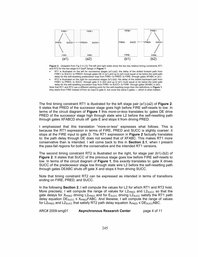
ARC# 2009-smg01 Asynchronous Research Center page 4 of 11
(a1) (a2) (b1) (b2)
Figure 2 (Adapted from Fig 2 in [1]) The left and right sides show the two key relative timing constraints RT1 and RT2 for the two-stage 6-4 GasP design in Figure 1:
RT1 is illustrated on the left for successive stages (a1)-(a2): the delay of the dotted forward path from FIRE+ to SUCC+ to PRED+ through gates DE in (a1) and up to (a2) must equal or be below the solid path delay for the self-resetting predecessor loop from FIRE+ to PRED- to FIRE- through gates XFABC in (a1).
RT2 is illustrated on the right for successive stages (b1)-(b2): the delay of the dotted backward path from FIRE+ to PRED- to SUCC- through gate X in (b2) and up to (b1) must equal or be below the solid path delay for the self-resetting successor loop from FIRE+ to SUCC+ to FIRE- through gates DEABC in (b2).
Note that RT1 and RT2 use a different starting point for the self-resetting loops than the definitions in Figure 1: they starts from FIRE instead of from an input to gate A, but cover the same 5 gates — which is what matters.
The first timing constraint RT1 is illustrated for the left stage pair (a1)-(a2) of Figure 2. It states that PRED of the successor stage goes high before FIRE self-resets to low. In terms of the circuit diagram of Figure 1 this more-or-less translates to: gates DE drive PRED of the successor stage high through state wire L2 before the self-resetting path through gates XFABCD shuts off gate E and stops it from driving PRED.
I emphasized that this translation ―more-or-less‖ expresses what follows. This is because the RT1 expression in terms of FIRE, PRED and SUCC is slightly coarser: it stops at the FIRE input to gate D. The RT1 expression in Figure 2 factually translates to: the path delay through DE does not exceed that of XFABC. This makes RT1 more conservative than is intended. I will come back to this in Section 2.1, when I present the pass-fail regions for both the conservative and the intended RT1 versions.
The second timing constraint RT2 is illustrated on the right, for stage pair (b1)-(b2) of Figure 2. It states that SUCC of the previous stage goes low before FIRE self-resets to low. In terms of the circuit diagram of Figure 1, this exactly translates to: gate X drives SUCC of the predecessor stage low through state wire L2 before the self-resetting path through gates DEABC shuts off gate X and stops it from driving SUCC.
Note that timing constraint RT2 can be expressed as intended in terms of transitions ending on FIRE, PRED, and SUCC.
In the following Section 2, I will compute the values for L2 for which RT1 and RT2 hold. More precisely, I will compute the range of values for L2PRED and L2SUCC so that the gate delays for XPRED driving L2PRED and for ESUCC driving L2SUCC satisfy the RT1 path delay equation DESUCC ≤ XPREDFABC. And likewise, I will compute the range of values for L2PRED and L2SUCC that satisfy RT2 path delay equation XPRED ≤ DESUCCABC.
245
ARC# 2009-smg01 Asynchronous Research Center page 5 of 11
2. Computing Allowable Module Distances I use the term allowable module distances to indicate the range of wire lengths between 6-4-GasP modules that satisfy relative timing constraints RT1 and RT2. RT1 and RT2 are path-delay constraints; they are computed from the delays of the gates and the wires on the corresponding paths. This paper adopts the wire model used by Joshi et al in [1]. This means that a wire is modeled as a lumped capacitance, and its delay is incorporated into the delay of each gate that drives this lumped capacitance. Delays due to wire resistance are ignored.
2
Joshi et al. built a spreadsheet that calculates the gate delays in a 6-4 GasP module using wire loads that are typical for the 90 nanometer chip design of Infinity.
3 The delay
calculations are based on the theory of Logical Effort [2]. Their spreadsheet calculations are repeated in Table 1 below. With the help of Table 1 I compute the range of allowable module distances. I will first compute the path delays for RT1 and from these the allowable module distances for RT1. This is done Section 2.1. In Section 2.2, I do the same for RT2. I combine the two results in Section 2.3, where I give the full picture and relate my results back to the 90 nanometer results of the Infinity test chip presented by Joshi et al. in [1].
Table 1 (Adapted from Table 2 in [1]). Below follow the Logical Effort calculations of each gate delay in the 6-4 GasP module of Figure 1.The three columns with bold numbers for S, P and WL are fixed by design: gate size S and its self-delay P follow from the gate implementation and the gate complexity, and wire load WL follows from the wire dimensions. Short wires are indicated as `wire’ (values taken from column WL); the long wires L1 and L2 are indicated explicitly. Note that the calculation of the self delay P for gates E and X counts the diffusion output capacitance of both E and X, because both their outputs connect to the state wire L2. Also note that the D2 values for E and X are different for different wire loads of L2. The Table uses the logical effort values of Table 1 in [1] (not included) to calculate the load per gate input: IL = (S * logical effort of the gate). The formulas for gate delay, wire load delay, and total delay are: D1 = GL/S, D2 = WL/S, Total = D1 + P + D2.
Gate Name
Size (S)
Load per
input (IL)
Drives next gates and wire
Next gate load
(GL)
Delay from GL (D1)
Self delay
(P)
Next wire load (WL)
Delay from WL (D2)
Total delay [τ]
3
A 18 30 B+wire 40 2.2 2 9 0.5 4.7
B 40 40 C+wire 100 2.5 1 20 0.5 4
C 100 100 D+X+ L1latches + L1wire 20+20+200 2.4 1 100 1 4.4
D 20 20 E+wire 40 2 1 20 1 4
F 10 10 A+wire 30 3 1 5 0.5 4.5
E L2=15
60 40 A+F+L2 30+10 0.67 with X
= 1 15 0.25 1.9
E L2=150
60 40 A+F+L2 30+10 0.67 with X
= 1 150 2.5 4.2
X L2=15
60 20 A+F+L2 30+10 0.67 with E
= 1 15 0.25 1.9
X L2=150
60 20 A+F+L2 30+10 0.67 with E
= 1 150 2.5 4.2
2 Delays due to wire resistance and other long wires effects will be included in a follow-up paper.
3 The delay unit here and in [1] is `τ’ (tau): the characteristic delay of an inverter in the given process.
246
ARC# 2009-smg01 Asynchronous Research Center page 6 of 11
2.1. Path Delays and Allowable Module Distances for RT1
From Figure 2(a1)-(a2) one can see that relative timing constraint RT1 involves both state wires at both ends of the 6-4 GasP module: the predecessor state wire participates in the solid backward path that self-resets FIRE from FIRE+ to FIRE-; the successor state wire participates in the dotted forward path from FIRE+ to PRED+.
To analyze RT1 it makes sense to distinguish these two state wires. I will use L2PRED to denote the state wire that connects the predecessor port PRED of a 6-4 GasP module to the previous stage. I will use L2SUCC to denote the state wire that connects the successor port SUCC of a 6-4 GasP module to the next stage. This matches with the terminology in Figure 1. For convenience, I wish to identify the gates that drive L2PRED respectively L2SUCC, so that the name of the gate indicates that the gate delay depends on the load value of L2PRED respectively L2SUCC. To this end, I rename gate X as XPRED and gate E as ESUCC.
In Section 1.2, I distinguished two RT1 constraints: a conservative version and the intended version. The conservative version, which I will call RT1conservative, states that the forward path delay from FIRE+ to SUCC+ to PRED+ through D and ESUCC must be less than or equal to the backward self-resetting path from FIRE+ to FIRE- through the series of gates XPRED, F, A, B and C. The intended RT1 constraint version, which I will call RT1intended, is similar, but has one more gate in the backward path: XPREDFABCD. I use the gate delay calculation procedure in Table 1 to compute the backward self-resetting path delays for XPREDFABC. For each fixed value of L2PRED, this gives me the maximum forward path delay for DESUCC for which RT1conservative holds. Given this, I reverse-engineer the calculation procedure in Table 1 to obtain the corresponding maximum load value of L2SUCC that satisfies RT1conservative.
4
The resulting difference in load values L2SUCC-L2PRED between the successor and predecessor state wires represents the maximum allowable module distance in terms of load capacity. I call this the margin value. L2SUCC-L2PRED values below the margin value pass the relative timing constraint, those above fail the constraint. The computations for the RT1conservative margin values are outlined in Table 2. It turns out that the margin value is approximately constant, 816 units of load, over the given range of L2PRED state wire loads.
5
4 The load capacitance unit here and in [1] is `X’: the gate load, or capacitance, of the smallest inverter
one can build in the given process. 5 Reminder: I have used a lumped wire load. I ignored long wire delay effects, which are outside the scope
of this study and which will be included in a follow-up paper.
247
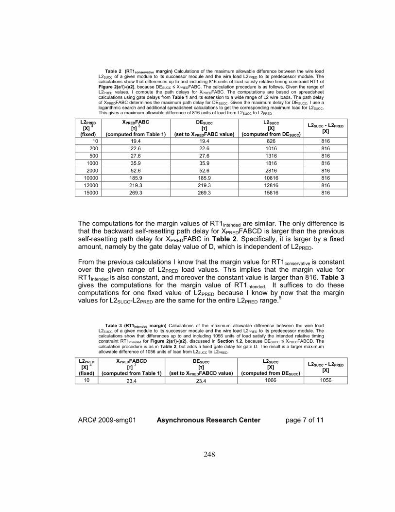
ARC# 2009-smg01 Asynchronous Research Center page 7 of 11
Table 2 (RT1conservative margin) Calculations of the maximum allowable difference between the wire load L2SUCC of a given module to its successor module and the wire load L2PRED to its predecessor module. The calculations show that differences up to and including 816 units of load satisfy relative timing constraint RT1 of Figure 2(a1)-(a2), because DESUCC ≤ XPREDFABC. The calculation procedure is as follows. Given the range of L2PRED values, I compute the path delays for XPREDFABC. The computations are based on spreadsheet calculations using gate delays from Table 1 and its extension to a wide range of L2 wire loads. The path delay of XPREDFABC determines the maximum path delay for DESUCC. Given the maximum delay for DESUCC, I use a logarithmic search and additional spreadsheet calculations to get the corresponding maximum load for L2SUCC. This gives a maximum allowable difference of 816 units of load from L2SUCC to L2PRED.
L2PRED
[X] 4
(fixed)
XPREDFABC
[τ] 3
(computed from Table 1)
DESUCC
[τ]
(set to XPREDFABC value)
L2SUCC
[X]
(computed from DESUCC)
L2SUCC - L2PRED
[X]
10 19.4 19.4 826 816
200 22.6 22.6 1016 816
500 27.6 27.6 1316 816
1000 35.9 35.9 1816 816
2000 52.6 52.6 2816 816
10000 185.9 185.9 10816 816
12000 219.3 219.3 12816 816
15000 269.3 269.3 15816 816
The computations for the margin values of RT1intended are similar. The only difference is that the backward self-resetting path delay for XPREDFABCD is larger than the previous self-resetting path delay for XPREDFABC in Table 2. Specifically, it is larger by a fixed amount, namely by the gate delay value of D, which is independent of L2PRED. From the previous calculations I know that the margin value for RT1conservative is constant over the given range of L2PRED load values. This implies that the margin value for RT1intended is also constant, and moreover the constant value is larger than 816. Table 3 gives the computations for the margin value of RT1intended. It suffices to do these computations for one fixed value of L2PRED because I know by now that the margin values for L2SUCC-L2PRED are the same for the entire L2PRED range.
5
Table 3 (RT1intended margin) Calculations of the maximum allowable difference between the wire load L2SUCC of a given module to its successor module and the wire load L2PRED to its predecessor module. The calculations show that differences up to and including 1056 units of load satisfy the intended relative timing constraint RT1intended for Figure 2(a1)-(a2), discussed in Section 1.2, because DESUCC ≤ XPREDFABCD. The calculation procedure is as in Table 2, but adds a fixed gate delay for gate D. The result is a larger maximum allowable difference of 1056 units of load from L2SUCC to L2PRED.
L2PRED
[X] 4
(fixed)
XPREDFABCD
[τ] 3
(computed from Table 1)
DESUCC
[τ]
(set to XPREDFABCD value)
L2SUCC
[X]
(computed from DESUCC)
L2SUCC - L2PRED
[X]
10 23.4 23.4 1066 1056
248
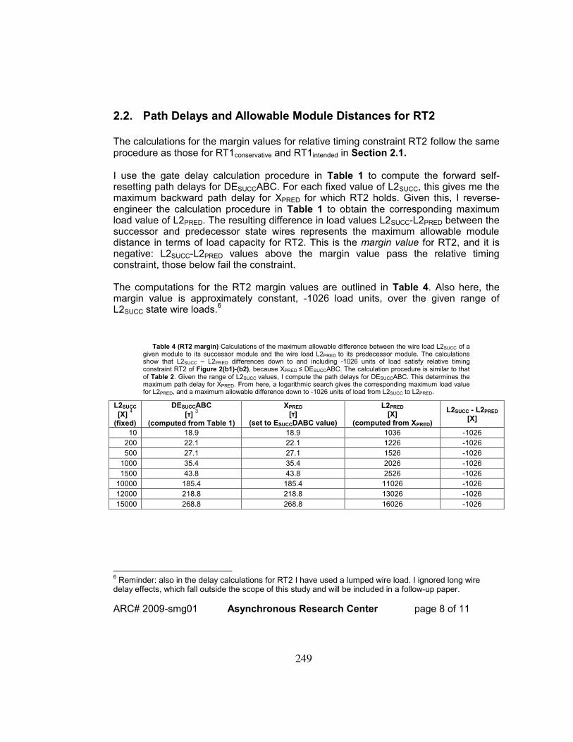
ARC# 2009-smg01 Asynchronous Research Center page 8 of 11
2.2. Path Delays and Allowable Module Distances for RT2
The calculations for the margin values for relative timing constraint RT2 follow the same procedure as those for RT1conservative and RT1intended in Section 2.1. I use the gate delay calculation procedure in Table 1 to compute the forward self-resetting path delays for DESUCCABC. For each fixed value of L2SUCC, this gives me the maximum backward path delay for XPRED for which RT2 holds. Given this, I reverse-engineer the calculation procedure in Table 1 to obtain the corresponding maximum load value of L2PRED. The resulting difference in load values L2SUCC-L2PRED between the successor and predecessor state wires represents the maximum allowable module distance in terms of load capacity for RT2. This is the margin value for RT2, and it is negative: L2SUCC-L2PRED values above the margin value pass the relative timing constraint, those below fail the constraint. The computations for the RT2 margin values are outlined in Table 4. Also here, the margin value is approximately constant, -1026 load units, over the given range of L2SUCC state wire loads.
6
Table 4 (RT2 margin) Calculations of the maximum allowable difference between the wire load L2SUCC of a given module to its successor module and the wire load L2PRED to its predecessor module. The calculations show that L2SUCC – L2PRED differences down to and including -1026 units of load satisfy relative timing constraint RT2 of Figure 2(b1)-(b2), because XPRED ≤ DESUCCABC. The calculation procedure is similar to that of Table 2. Given the range of L2SUCC values, I compute the path delays for DESUCCABC. This determines the maximum path delay for XPRED. From here, a logarithmic search gives the corresponding maximum load value for L2PRED, and a maximum allowable difference down to -1026 units of load from L2SUCC to L2PRED.
L2SUCC
[X] 4
(fixed)
DESUCCABC
[τ] 3
(computed from Table 1)
XPRED
[τ]
(set to ESUCCDABC value)
L2PRED
[X]
(computed from XPRED)
L2SUCC - L2PRED
[X]
10 18.9 18.9 1036 -1026
200 22.1 22.1 1226 -1026
500 27.1 27.1 1526 -1026
1000 35.4 35.4 2026 -1026
1500 43.8 43.8 2526 -1026
10000 185.4 185.4 11026 -1026
12000 218.8 218.8 13026 -1026
15000 268.8 268.8 16026 -1026
6 Reminder: also in the delay calculations for RT2 I have used a lumped wire load. I ignored long wire
delay effects, which fall outside the scope of this study and will be included in a follow-up paper.
249
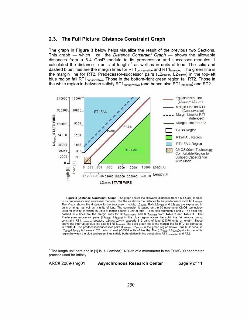
ARC# 2009-smg01 Asynchronous Research Center page 9 of 11
2.3. The Full Picture: Distance Constraint Graph
The graph in Figure 3 below helps visualize the result of the previous two Sections. This graph — which I call the Distance Constraint Graph — shows the allowable distances from a 6-4 GasP module to its predecessor and successor modules. I calculated the distance in units of length
7 as well as in units of load. The solid and
dashed blue lines are the margin lines for RT1conservative and RT1intended. The green line is the margin line for RT2. Predecessor-successor pairs (L2PRED, L2SUCC) in the top-left blue region fail RT1conservative. Those in the bottom-right green region fail RT2. Those in the white region in-between satisfy RT1conservative (and hence also RT1intended) and RT2.
Figure 3 (Distance Constraint Graph) The graph shows the allowable distances from a 6-4 GasP module
to its predecessor and successor modules. The X-axis shows the distance to the predecessor module, L2PRED. The Y-axis shows the distance to the successor module, L2SUCC. Both L2PRED and L2SUCC are expressed in units of length as well as in units of load. The conversion is based on the 90 nanometer CMOS technology used for Infinity, in which 36 units of length equals 1 unit of load — see also footnotes 4 and 7. The solid and dashed blue lines are the margin lines for RT1conservative and RT1intended from Table 2 and Table 3. The Predecessor-successor pairs (L2PRED, L2SUCC) in the blue region above the solid line fail relative timing constraint RT1conservative because L2SUCC-L2PRED exceeds 816 units of load (29376 units of length). Those above the interrupted blue line also fail RT1intended. The solid green line is the margin line for RT2, as computed in Table 4. The predecessor-successor pairs (L2PRED, L2SUCC) in the green region below it fail RT2 because L2SUCC-L2PRED is below -1026 units of load (-36936 units of length). The (L2PRED, L2SUCC)-pairs in the white region between the blue and green lines satisfy both relative timing constraints RT1conservative and RT2.
7 The length unit here and in [1] is `λ’ (lambda): 1/20-th of a micrometer in the TSMC 90 nanometer
process used for Infinity.
250
ARC# 2009-smg01 Asynchronous Research Center page 10 of 11
In addition to the allowable module distances and their relation to the key relative timing constraints, Figure 3 shows two other interesting facts.
1. The red equidistance line where L2PRED and L2SUCC have the same load and length falls in the PASS region, approximately midway between the margin lines for RT1intended and RT2. This is good news: it makes designing GasP systems easier because the designer can assume equidistant module distances and still leave adequate margins to place and route the modules.
2. The orange-striped square box of about 333 x 333 units of load in the bottom-left
corner of the graph represents the short-to-medium length wire region for the TSMC 90 nanometer CMOS manufacturing process that was used for Infinity. In this process, 333 units of wire load correspond to approximately 12000 units of wire length. This is the comfort region for the lumped capacitance wire model. The anticipation is that for wires longer than 12000 units, the wire resistance is no longer negligible, and neither are the rise and fall times of the wire transitions. To mitigate these long wire effects, one can insert extra 6-4 GasP modules, called repeater modules, at state wire intervals of 12000 units of length. Note that the orange-striped box is completely within the white PASS region of Figure 3. So, apparently, the repeater constraints to avoid long wires are much stricter than the 6-4 GasP relative timing constraints for functional correctness.
8
3. Conclusion The 6-4 GasP modules discussed in this paper are used to route data. The operation of each module is limited by relative timing constraints. In [1] Joshi et al. identified two key constraints, called RT1 and RT2, that limit the module distance between successive GasP modules in the router network. They also set up a framework to validate whether the distances from a 6-4 GasP module to its predecessor and successor are allowed. In this paper, I introduce a new representation, the Distance Constraint Graph, to visualize the relation between the allowable module distances and the relative timing constraints RT1 and RT2. By looking at the graph one can immediately locate the pass and fail regions for each constraint for up to 15000 load units, i.e. 540000 length units. There is one caveat: my current calculations ignore long wire effects — these will be taken into account in a follow-up paper.
9
8 I surely will investigate this further in my long-wire analysis.
9 See also footnotes 5, 6 and 8.
251
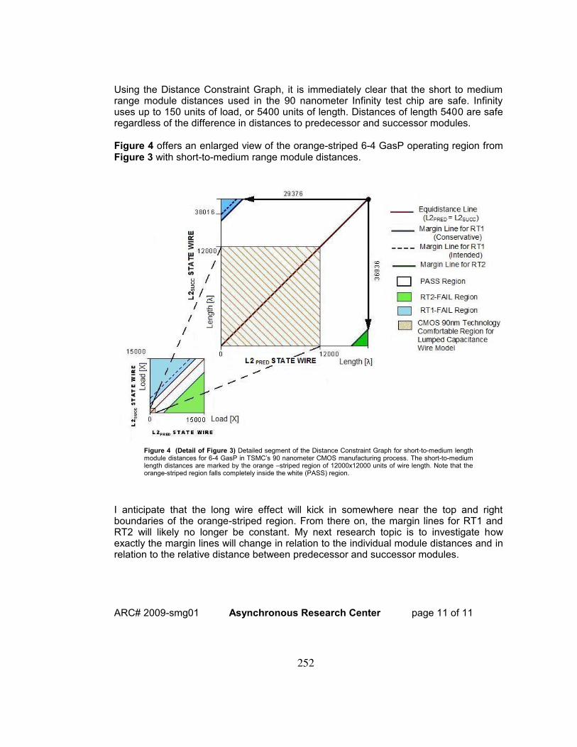
ARC# 2009-smg01 Asynchronous Research Center page 11 of 11
Using the Distance Constraint Graph, it is immediately clear that the short to medium range module distances used in the 90 nanometer Infinity test chip are safe. Infinity uses up to 150 units of load, or 5400 units of length. Distances of length 5400 are safe regardless of the difference in distances to predecessor and successor modules. Figure 4 offers an enlarged view of the orange-striped 6-4 GasP operating region from Figure 3 with short-to-medium range module distances.
Figure 4 (Detail of Figure 3) Detailed segment of the Distance Constraint Graph for short-to-medium length module distances for 6-4 GasP in TSMC’s 90 nanometer CMOS manufacturing process. The short-to-medium length distances are marked by the orange –striped region of 12000x12000 units of wire length. Note that the orange-striped region falls completely inside the white (PASS) region.
I anticipate that the long wire effect will kick in somewhere near the top and right boundaries of the orange-striped region. From there on, the margin lines for RT1 and RT2 will likely no longer be constant. My next research topic is to investigate how exactly the margin lines will change in relation to the individual module distances and in relation to the relative distance between predecessor and successor modules.
252
Appendix O
BONUS MATERIAL: SHORT-TO-MEDIUM-TO-LONGWIRE STUDY
c!2010 IEEE. Reprinted with permission, from the following publication source:
• Swetha Mettala Gilla, Marly Roncken and Ivan Sutherland. Long-Range GasPwith Charge Relaxation. In Proc. IEEE International Symposium on Asyn-chronous Circuits and Systems (ASYNC), pages 185–195, 2010.
This IEEE publication can also be found in the thesis reference list as reference [18].
253
Long-Range GasP with Charge Relaxation
Swetha Mettala Gilla, Marly Roncken, and Ivan [email protected], [email protected], [email protected]
Asynchronous Research CenterMaseeh College of Engineering and Computer Science
Portland State University, Portland, Oregon, USA
Abstract
GasP circuit modules communicate handshake signals intwo directions over a single state wire. The 2008 Infinity testchip demonstrated GasP in 90 nm CMOS operating at fourgiga data items per second, but revealed that state wiresabout 5000 lambda long retard operation by about 10%.
Simulations reported in this paper show that GasP mod-ules will tolerate surprisingly long state wires, albeit at re-duced throughput. The modules appear to operate correctlywith state wires whose delay exceeds the drive time. Withsuch long wires, the receiving module waits until passivedistribution of charge brings the wire within range of thereceiver’s switching threshold. Having put enough chargeinto the wire, or vice-versa removed enough charge from it,the sending module may proceed with its next task. This re-sult applies equally to other single-track signaling methods.
This behavior calls for a new kind of relative timing con-straint to address when the wire charging or dischargingprocess may cease rather than when the signal reaches thefar end of the wire.
Keywords: GasP, Infinity chip, long wires, single-track,on-chip communication, self-timed, asynchronous circuits.
1 Introduction
Since publication of the first GasP family of circuits in2001 [15] we have built and tested a variety of GasP chips.One chip experiment, called Infinity, consists of two ringsof 100 GasP modules each that share a common section of50 modules. The GasP modules in the Infinity test chip,which includes the Infinity experiment, form the basis of awide variety of network-on-chip topologies. A sketch of thelayout of the Infinity experiment appears in Figure 1(a).
Figure 1(b) offers a canopy diagram for separate operationof the two rings in Infinity. For this experiment data cir-culate in a single ring, avoiding contention for use of the
50-stage shared section. The work reported in this paper be-gan with the observation of the flat tops in this (measured)canopy diagram. The maximum throughput indicated bythe two flat tops is about 10% below the peak throughput inFigure 1(c) as measured for other GasP rings on the chip.1
Additional experiments traced the 10% loss in throughputobserved in Infinity to the longer state wires that connect thecommon ring section in the center column of Figure 1(a) tothe individual ring sections in the side columns. The statewires from column to column are about 5000 lambda long,whereas the state wires within each column are only about500 lambda long. This phenomenon prompted us to studythe effect of wire delays in GasP.
Our first study, published by Joshi et al. in [5], uses alumped capacitance model to examine the impact of a longstate wire. It presents a logical effort model to compute thegate and path delays in GasP operations and to analyze therelative timing constraints on which the correct operationof a GasP module depends [16, 12]. We observed that if themain effect of the long wire is to retard its driver, GasP mod-ules should operate correctly over a large range of distances.Our analysis predicts correct operation provided the differ-ence in the distances to predecessor and successor modulesis limited. It predicts failure if these distances differ by toomuch. Moreover, the extra delay computed for the lumpedcapacitance model of a 5000 lambda long wire explains the10% loss in throughput observed in Infinity.
However, the predicted maximum difference in module dis-tances in the study by Joshi et al. is large enough to castdoubt on the adequacy of the lumped capacitance wiremodel, in particular for wires longer than 5000 lambda.Therefore, we started a second study that uses better models
1Silicon experiments and simulations in this paper all use a 90 nmCMOS process by TSMC in which lambda (λ) is 50 nm and tau (τ ) isabout 8 psec. We prefer to use the process-normalized metrics lambdaand tau rather than absolute metrics so as to make our results more readilyapplicable to other manufacturing processes.
2010 IEEE Symposium on Asynchronous Circuits and Systems
978-0-7695-4032-0/10 $26.00 © 2010 IEEEDOI 10.1109/ASYNC.2010.26
185
254
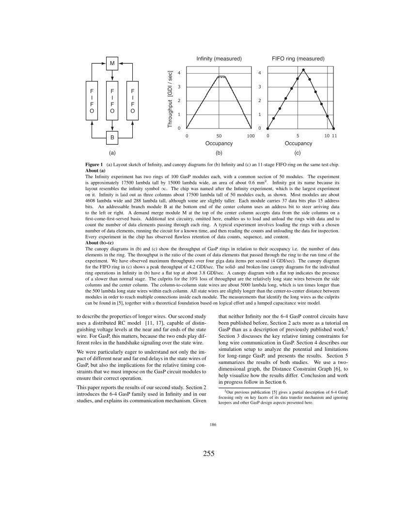
FIFO
FIFO
FIFO
M
B
0
1
2
3
4
0
1
2
3
4
0 5 10 110 50 100
Occupancy Occupancy
Thr
ough
put
[GD
I / s
ec]
(a) (b) (c)
FIFO ring (measured)Infinity (measured)
Figure 1 (a) Layout sketch of Infinity, and canopy diagrams for (b) Infinity and (c) an 11-stage FIFO ring on the same test chip.About (a)The Infinity experiment has two rings of 100 GasP modules each, with a common section of 50 modules. The experimentis approximately 17500 lambda tall by 15000 lambda wide, an area of about 0.6 mm2. Infinity got its name because itslayout resembles the infinity symbol ∞. The chip was named after the Infinity experiment, which is the largest experimenton it. Infinity is laid out as three columns about 17500 lambda tall of 50 modules each, as shown. Most modules are about4608 lambda wide and 288 lambda tall, although some are slightly taller. Each module carries 37 data bits plus 15 addressbits. An addressable branch module B at the bottom end of the center column uses an address bit to steer arriving datato the left or right. A demand merge module M at the top of the center column accepts data from the side columns on afirst-come-first-served basis. Additional test circuitry, omitted here, enables us to load and unload the rings with data and tocount the number of data elements passing through each ring. A typical experiment involves loading the rings with a chosennumber of data elements, running the circuit for a known time, and then reading the counts and unloading the data for inspection.Every experiment in the chip has observed flawless retention of data counts, sequence, and content.About (b)–(c)The canopy diagrams in (b) and (c) show the throughput of GasP rings in relation to their occupancy i.e. the number of dataelements in the ring. The throughput is the ratio of the count of data elements that passed through the ring to the run time of theexperiment. We have observed maximum throughputs over four giga data items per second (4 GDI/sec). The canopy diagramfor the FIFO ring in (c) shows a peak throughput of 4.2 GDI/sec. The solid- and broken-line canopy diagrams for the individualring operations in Infinity in (b) have a flat top at about 3.8 GDI/sec. A canopy diagram with a flat top indicates the presenceof a slower than normal stage. The culprits for the 10% loss of throughput are the relatively long state wires between the sidecolumns and the center column. The column-to-column state wires are about 5000 lambda long, which is ten times longer thanthe 500 lambda long state wires within each column. All state wires are slightly longer than the center-to-center distance betweenmodules in order to reach multiple connections inside each module. The measurements that identify the long wires as the culpritscan be found in [5], together with a theoretical foundation based on logical effort and a lumped capacitance wire model.
to describe the properties of longer wires. Our second studyuses a distributed RC model [11, 17], capable of distin-guishing voltage levels at the near and far ends of the statewire. For GasP, this matters, because the two ends play dif-ferent roles in the handshake signaling over the state wire.
We were particularly eager to understand not only the im-pact of different near and far end delays in the state wires ofGasP, but also the implications for the relative timing con-straints that we must impose on the GasP circuit modules toensure their correct operation.
This paper reports the results of our second study. Section 2introduces the 6-4 GasP family used in Infinity and in ourstudies, and explains its communication mechanism. Given
that neither Infinity nor the 6-4 GasP control circuits havebeen published before, Section 2 acts more as a tutorial onGasP than as a description of previously published work.2
Section 3 discusses the key relative timing constraints forlong wire communication in GasP. Section 4 describes oursimulation setup to analyze the potential and limitationsfor long-range GasP, and presents the results. Section 5summarizes the results of both studies. We use a two-dimensional graph, the Distance Constraint Graph [6], tohelp visualize how the results differ. Conclusion and workin progress follow in Section 6.
2Our previous publication [5] gives a partial description of 6-4 GasP,focusing only on key facets of its data transfer mechanism and ignoringkeepers and other GasP design aspects presented here.
186
255
2 GasP Modules
Infinity uses 6-4 GasP [14]. The 6-4 GasP family gets itsname from the six logic gates on the path going forwardfrom one module to the next, path ABCDEF in Figure 2,and from the four logic gates on the path going backwards,path ABCX. The longer delay is in the forward directionbecause that is the direction in which the data elements aretransferred. Copying data requires action on the part of thedata latches, whereas moving an empty space or “bubble”backwards to declare the latches empty needs no action.
Figure 2 shows a 2-stage FIFO, with one 6-4 GasP moduleper stage. The two stages, M1 and M2, are connected bya bidirectional state wire L2 via ports SUCC1 and PRED2.When state wire L2 is high it indicates that M1 has new datafor M2. We will refer to this as L2 being full. When statewire L2 is low it indicates that M2 has latched the proffereddata and it is safe for M1 to change its data. We will referto this as L2 being empty.3
When PRED2 is high and SUCC2 low, meaning M1 hasnew data for M2 and M2 has space for it, M2 raises itssignal FIRE2. A high FIRE2 signal starts three parallel ac-tions: (1) the data latches of stage M2 are enabled to copythe proffered data, and (2) SUCC2 is raised via gates D andE to indicate to M2’s successor that new data are available,and (3) PRED2 is lowered via gate X to declare L2 empty.
Note that for FIRE2 to rise, gate A must synchronize a highPRED2 signal with a low SUCC2 signal. But to get FIRE2
to fall, either a low PRED2 signal or a high SUCC2 signalsuffices. Hence, actions (2) and (3) each have the additionalside effect of resetting FIRE2.
So, setting FIRE2 high automatically leads to resettingFIRE2 low, and there is a choice of two self-resetting loopsthat automate this: the forward loop DEABC, and the back-ward loop XFABC. Note that each loop has five gates.
The gate count matters. GasP modules are custom-designedusing logical effort [16]. The transistors in each logic gateare sized such that all logic gates have approximately thesame delay. Gate sizing takes into account both the transis-tor sizes of the driven gates and the loads of the connectingwires. As a result, we can count delay in terms of logic gatedelays and we can compare path delays simply by countingand comparing the number of gates on each path.
This works as long as we can adequately predict the wirelengths. Gates A, B, D and F in Figure 2 each drive a singlelocal gate, and so we may assume that the connecting wirelengths are known in advance.
3This paper addresses primarily the control portion of 6-4 GasP thatgenerates the handshake operations between GasP modules. Other thangiving an intuition of the data bundling relation between the handshakesignaling on state wire L2 and the data being transferred, we omit anyfurther discussion of data validity.
The situation for gate C is more complicated: C drives twolocal gates, D and X. In addition, C drives a number oflatches and the not so local wire L1 between gates D andX and the latches. In Infinity, the data latches are placednear the 6-4 GasP module that controls them. GasP moduleand latches together form a macro module with a fixed wirelength for L1. This solves the gate sizing problem for C.
The exceptions are gates E and X that drive the L2 statewire. The length of L2 depends on the distance between themodules, and this is unknown until the system layout hasbeen finalized. If E and X are sized using the wire lengthsfor A, B, D and F, as was done in Infinity, the gate delaysfor E and X will vary with different module distances andthe throughput will vary accordingly, as demonstrated bythe canopy diagrams in Figure 1(b)–(c).
So, without further investigation into the effects of longstate wires, all we can say is that, for short state wires,the maximum throughput of 6-4 GasP is the throughput thatcorresponds to a cycle time of 10 gate delays: 6 to forwardthe data and 4 to move the empty space backward. The in-vestigation with long state wires follows in Section 4, and iseasier to understand after reading the design details on statewires and keepers coming up next.
2.1 State Wires
GasP state wires use a form of forward and back handshakeprotocol, called “single-track” signaling [1, 15, 9, 2]. In asingle-track protocol, a single wire carries both the forwardand the backward handshake signals. This is attractive, notonly because a single wire occupies less space, but also be-cause the handshake consumes minimum energy per cycle.To handshake, a transition must pass in each direction. Thesingle wire does exactly that, with automatic return to theinitial state after each pair of handshake signals.
The GasP modules in this paper use single-track handshakesignaling to communicate control information only. Theyuse single-rail signaling to communicate data, as do thehandshake circuits discussed by van Berkel and Bink in [1].The single-track designs discussed by Nystrom et al. in [9]combine both the data and the control into a single-trackcommunication protocol, as do Ferretti and Beerel in [2].
There are various ways to implement single-track signaling;van Berkel and Bink differentiate between “dynamic” and“overlapping” protocols [1]. Each participant in a single-track signaling protocol must cease to drive the state wiresoon enough to make room for the action of the other par-ticipant. Were one participant to drive the wire for too long,then both might end up driving it concurrently in oppositedirections, consuming unnecessary energy and producingan indeterminate logic signal. How is this to be avoided?
187
256
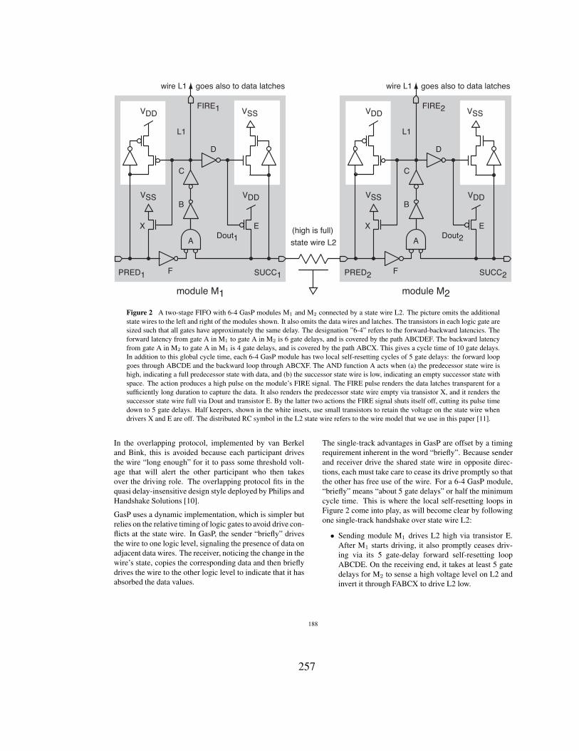
PRED1 SUCC1
A
B
F
D
C
EX
FIRE1
Dout1
VDDVSS
VSSVDD
PRED2 SUCC2
wire L1 goes also to data latches
A
B
F
D
C
EX
FIRE2
Dout2
VDDVSS
VSSVDD
state wire L2
(high is full)
wire L1 goes also to data latches
module M1 module M2
L1L1
Figure 2 A two-stage FIFO with 6-4 GasP modules M1 and M2 connected by a state wire L2. The picture omits the additionalstate wires to the left and right of the modules shown. It also omits the data wires and latches. The transistors in each logic gate aresized such that all gates have approximately the same delay. The designation ”6-4” refers to the forward-backward latencies. Theforward latency from gate A in M1 to gate A in M2 is 6 gate delays, and is covered by the path ABCDEF. The backward latencyfrom gate A in M2 to gate A in M1 is 4 gate delays, and is covered by the path ABCX. This gives a cycle time of 10 gate delays.In addition to this global cycle time, each 6-4 GasP module has two local self-resetting cycles of 5 gate delays: the forward loopgoes through ABCDE and the backward loop through ABCXF. The AND function A acts when (a) the predecessor state wire ishigh, indicating a full predecessor state with data, and (b) the successor state wire is low, indicating an empty successor state withspace. The action produces a high pulse on the module’s FIRE signal. The FIRE pulse renders the data latches transparent for asufficiently long duration to capture the data. It also renders the predecessor state wire empty via transistor X, and it renders thesuccessor state wire full via Dout and transistor E. By the latter two actions the FIRE signal shuts itself off, cutting its pulse timedown to 5 gate delays. Half keepers, shown in the white insets, use small transistors to retain the voltage on the state wire whendrivers X and E are off. The distributed RC symbol in the L2 state wire refers to the wire model that we use in this paper [11].
In the overlapping protocol, implemented by van Berkeland Bink, this is avoided because each participant drivesthe wire “long enough” for it to pass some threshold volt-age that will alert the other participant who then takesover the driving role. The overlapping protocol fits in thequasi delay-insensitive design style deployed by Philips andHandshake Solutions [10].
GasP uses a dynamic implementation, which is simpler butrelies on the relative timing of logic gates to avoid drive con-flicts at the state wire. In GasP, the sender “briefly” drivesthe wire to one logic level, signaling the presence of data onadjacent data wires. The receiver, noticing the change in thewire’s state, copies the corresponding data and then brieflydrives the wire to the other logic level to indicate that it hasabsorbed the data values.
The single-track advantages in GasP are offset by a timingrequirement inherent in the word “briefly”. Because senderand receiver drive the shared state wire in opposite direc-tions, each must take care to cease its drive promptly so thatthe other has free use of the wire. For a 6-4 GasP module,“briefly” means “about 5 gate delays” or half the minimumcycle time. This is where the local self-resetting loops inFigure 2 come into play, as will become clear by followingone single-track handshake over state wire L2:
• Sending module M1 drives L2 high via transistor E.After M1 starts driving, it also promptly ceases driv-ing via its 5 gate-delay forward self-resetting loopABCDE. On the receiving end, it takes at least 5 gatedelays for M2 to sense a high voltage level on L2 andinvert it through FABCX to drive L2 low.
188
257
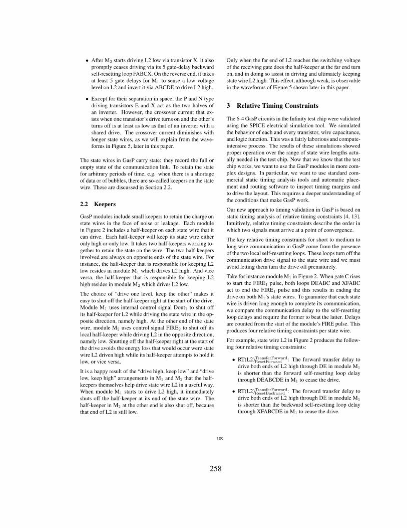
• After M2 starts driving L2 low via transistor X, it alsopromptly ceases driving via its 5 gate-delay backwardself-resetting loop FABCX. On the reverse end, it takesat least 5 gate delays for M1 to sense a low voltagelevel on L2 and invert it via ABCDE to drive L2 high.
• Except for their separation in space, the P and N typedriving transistors E and X act as the two halves ofan inverter. However, the crossover current that ex-ists when one transistor’s drive turns on and the other’sturns off is at least as low as that of an inverter with ashared drive. The crossover current diminishes withlonger state wires, as we will explain from the wave-forms in Figure 5, later in this paper.
The state wires in GasP carry state: they record the full orempty state of the communication link. To retain the statefor arbitrary periods of time, e.g. when there is a shortageof data or of bubbles, there are so-called keepers on the statewire. These are discussed in Section 2.2.
2.2 Keepers
GasP modules include small keepers to retain the charge onstate wires in the face of noise or leakage. Each modulein Figure 2 includes a half-keeper on each state wire that itcan drive. Each half-keeper will keep its state wire eitheronly high or only low. It takes two half-keepers working to-gether to retain the state on the wire. The two half-keepersinvolved are always on opposite ends of the state wire. Forinstance, the half-keeper that is responsible for keeping L2low resides in module M1 which drives L2 high. And viceversa, the half-keeper that is responsible for keeping L2high resides in module M2 which drives L2 low.
The choice of ”drive one level, keep the other” makes iteasy to shut off the half-keeper right at the start of the drive.Module M1 uses internal control signal Dout1 to shut offits half-keeper for L2 while driving the state wire in the op-posite direction, namely high. At the other end of the statewire, module M2 uses control signal FIRE2 to shut off itslocal half-keeper while driving L2 in the opposite direction,namely low. Shutting off the half-keeper right at the start ofthe drive avoids the energy loss that would occur were statewire L2 driven high while its half-keeper attempts to hold itlow, or vice versa.
It is a happy result of the “drive high, keep low” and “drivelow, keep high” arrangements in M1 and M2 that the half-keepers themselves help drive state wire L2 in a useful way.When module M1 starts to drive L2 high, it immediatelyshuts off the half-keeper at its end of the state wire. Thehalf-keeper in M2 at the other end is also shut off, becausethat end of L2 is still low.
Only when the far end of L2 reaches the switching voltageof the receiving gate does the half-keeper at the far end turnon, and in doing so assist in driving and ultimately keepingstate wire L2 high. This effect, although weak, is observablein the waveforms of Figure 5 shown later in this paper.
3 Relative Timing Constraints
The 6-4 GasP circuits in the Infinity test chip were validatedusing the SPICE electrical simulation tool. We simulatedthe behavior of each and every transistor, wire capacitance,and logic function. This was a fairly laborious and compute-intensive process. The results of these simulations showedproper operation over the range of state wire lengths actu-ally needed in the test chip. Now that we know that the testchip works, we want to use the GasP modules in more com-plex designs. In particular, we want to use standard com-mercial static timing analysis tools and automatic place-ment and routing software to inspect timing margins andto drive the layout. This requires a deeper understanding ofthe conditions that make GasP work.
Our new approach to timing validation in GasP is based onstatic timing analysis of relative timing constraints [4, 13].Intuitively, relative timing constraints describe the order inwhich two signals must arrive at a point of convergence.
The key relative timing constraints for short to medium tolong wire communication in GasP come from the presenceof the two local self-resetting loops. These loops turn off thecommunication drive signal to the state wire and we mustavoid letting them turn the drive off prematurely.
Take for instance module M1 in Figure 2. When gate C risesto start the FIRE1 pulse, both loops DEABC and XFABCact to end the FIRE1 pulse and this results in ending thedrive on both M1’s state wires. To guarantee that each statewire is driven long enough to complete its communication,we compare the communication delay to the self-resettingloop delays and require the former to beat the latter. Delaysare counted from the start of the module’s FIRE pulse. Thisproduces four relative timing constraints per state wire.
For example, state wire L2 in Figure 2 produces the follow-ing four relative timing constraints:
• RT(L2)TransferForwardResetForward : The forward transfer delay to
drive both ends of L2 high through DE in module M1
is shorter than the forward self-resetting loop delaythrough DEABCDE in M1 to cease the drive.
• RT(L2)TransferForwardResetBackward : The forward transfer delay to
drive both ends of L2 high through DE in module M1
is shorter than the backward self-resetting loop delaythrough XFABCDE in M1 to cease the drive.
189
258
PRED1 SUCC10
GasPM1
GasPM2
GasPM3
GasPM4
GasPM5
GasPM6
GasPM7
GasPM8
GasPM10
GasPM9
long state wire
F E E E E E E E E
E
Dout10FIRE1
Figure 3 Our long-range GasP simulation set up includes a ring of ten 6-4 GasP modules, M1 to M10, connected by nine shortstate wires and one long state wire. The circles with designation E or F indicate the initial states of the state wires: E for empty,i.e. low, and F for full, i.e. high. The ring in this picture starts with one full state wire. The picture explicitly indicates the GasPsignals PRED1 and FIRE1 of module M1 and SUCC10 and Dout10 of module M10. These are the signals that play a direct role inthe handshake communication over the long wire. The picture omits the corresponding signals for the other 6-4 GasP modules.
• RT(L2)TransferBackwardResetForward : The backward transfer delay
to drive both ends of L2 low through X in moduleM2 is shorter than the forward self-resetting loop delaythrough DEABCX in M2 to cease the drive.
• RT(L2)TransferBackwardResetBackward : The backward transfer delay
to drive both ends of L2 low through X in module M2
is shorter than the backward self-resetting loop delaythrough XFABCX in M2 to cease the drive.
The M.Sc. thesis by Prasad Joshi [4] shows how to validaterelative timing constraints for a given GasP design usingPrimeTime, the Synopsys static timing analysis tool.
4 Long-Range GasP Simulations
To develop our understanding of long state wires in GasPwe undertook a series of simulations.
First, we simulated the behavior of isolated long wires us-ing a distributed RC model. We used four R-C-R sectionsfor every 100 lambda of wire, matching the corresponding90 nm TSMC wire resistance and capacitance numbers forstate wires. We simulated the wire delays for wire lengthsranging from 100 to 60000 lambda. We observed that thedelay in the wire is, as expected, roughly quadratic withits length. However, for longer wires, the far end of thewire exhibits very slow rise times which renders the precisemeaning of “wire delay” suspect. We observed reasonabledelays for wires up to 30000 lambda, or 1.5 mm, long.
Armed with these observations, we set up simulations of 6-4GasP modules separated by long state wires. Each simula-tion involves a ring of ten 6-4 GasP modules with nine shortand exactly one long state wire. Different initializations ofthe state wires permit us to generate a canopy diagram toexhibit the impact of the long wire on throughput. The twoextreme initializations for data-limited rings, with exactly
one full state wire, and for bubble-limited rings, with ex-actly one empty state wire, will give us a larger time win-dow to observe the dynamic aspects of the long wire andits keepers. Figure 3 shows the simulation set up for thedata-limited case with exactly one full state wire.
We simulated each initial configuration with the long statewire set at a length of 1000, 4000, 10000, 20000, 24000,and 30000 lambda. To get reasonable simulation times, weused three R-C-R sections for every 1000 lambda of wire.This still produces a sufficiently fine-grained wire model.All simulated configurations with long state wire lengths upto and including 24000 lambda run correctly.
For the 30000 lambda long state wire we observed failuresin the two extreme initialization scenarios with (a) exactlyone full state wire and (b) exactly one empty state wire:
(a) When we start with one full state wire, initialized as inFigure 3, we lose the full state during the first hand-shake over the 30000 lambda long state wire, becausemodule M10 shuts off its high drive before the wire hasaccumulated enough charge to rise from ground levelto the switching voltage level of M1. The ring, nowcompletely empty with nothing to work on, deadlocks.
(b) When we start with one empty state wire, or bubble,we see not a loss of the one and only bubble but thecreation of an extra bubble. This is due to the fact thatwe initialized the ring with the empty state at the longstate wire. During the first handshake over the 30000lambda long state wire, module M10 behaves exactlylike it did in the previous scenario: it shuts off its highdrive before the wire has accumulated enough chargeto rise from ground level to the switching level of M1.And so, we end up with two bubbles instead of one.With two bubbles, the round trip delay becomes justshort enough to keep the ring going.
190
259
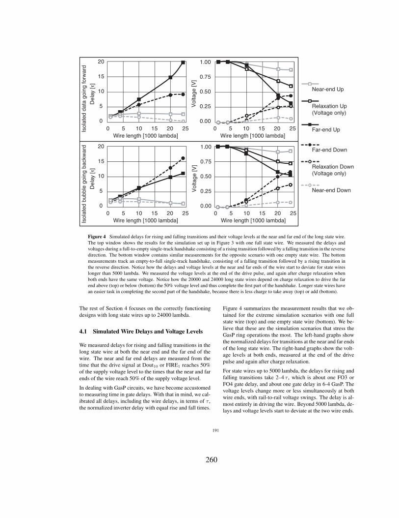
De
lay
[τ]
Vol
tage
[V]
0.00
0.25
0.50
0.75
1.00
De
lay
[τ]
Vol
tage
[V]
0.00
0.25
0.50
0.75
1.00
Wire length [1000 lambda] Wire length [1000 lambda]
Wire length [1000 lambda] Wire length [1000 lambda]
Far-end Down
Far-end Up
Near-end Down
Relaxation Up(Voltage only)
Relaxation Down(Voltage only)
Near-end Up
0
5
10
15
20
0 5 10 15 20 25 0
0
5
10
15
20
0
5 10 15 20 25
0 5 10 15 20 25 5 10 15 20 25
Isol
ated
dat
a go
ing
forw
ard
Isol
ated
bub
ble
goin
g ba
ckw
ard
Figure 4 Simulated delays for rising and falling transitions and their voltage levels at the near and far end of the long state wire.The top window shows the results for the simulation set up in Figure 3 with one full state wire. We measured the delays andvoltages during a full-to-empty single-track handshake consisting of a rising transition followed by a falling transition in the reversedirection. The bottom window contains similar measurements for the opposite scenario with one empty state wire. The bottommeasurements track an empty-to-full single-track handshake, consisting of a falling transition followed by a rising transition inthe reverse direction. Notice how the delays and voltage levels at the near and far ends of the wire start to deviate for state wireslonger than 5000 lambda. We measured the voltage levels at the end of the drive pulse, and again after charge relaxation whenboth ends have the same voltage. Notice how the 20000 and 24000 long state wires depend on charge relaxation to drive the farend above (top) or below (bottom) the 50% voltage level and thus complete the first part of the handshake. Longer state wires havean easier task in completing the second part of the handshake, because there is less charge to take away (top) or add (bottom).
The rest of Section 4 focuses on the correctly functioningdesigns with long state wires up to 24000 lambda.
4.1 Simulated Wire Delays and Voltage Levels
We measured delays for rising and falling transitions in thelong state wire at both the near end and the far end of thewire. The near and far end delays are measured from thetime that the drive signal at Dout10 or FIRE1 reaches 50%of the supply voltage level to the times that the near and farends of the wire reach 50% of the supply voltage level.
In dealing with GasP circuits, we have become accustomedto measuring time in gate delays. With that in mind, we cal-ibrated all delays, including the wire delays, in terms of τ ,the normalized inverter delay with equal rise and fall times.
Figure 4 summarizes the measurement results that we ob-tained for the extreme simulation scenarios with one fullstate wire (top) and one empty state wire (bottom). We be-lieve that these are the simulation scenarios that stress theGasP ring operations the most. The left-hand graphs showthe normalized delays for transitions at the near and far endsof the long state wire. The right-hand graphs show the volt-age levels at both ends, measured at the end of the drivepulse and again after charge relaxation.
For state wires up to 5000 lambda, the delays for rising andfalling transitions take 2–4 τ , which is about one FO3 orFO4 gate delay, and about one gate delay in 6-4 GasP. Thevoltage levels change more or less simultaneously at bothwire ends, with rail-to-rail voltage swings. The delay is al-most entirely in driving the wire. Beyond 5000 lambda, de-lays and voltage levels start to deviate at the two wire ends.
191
260
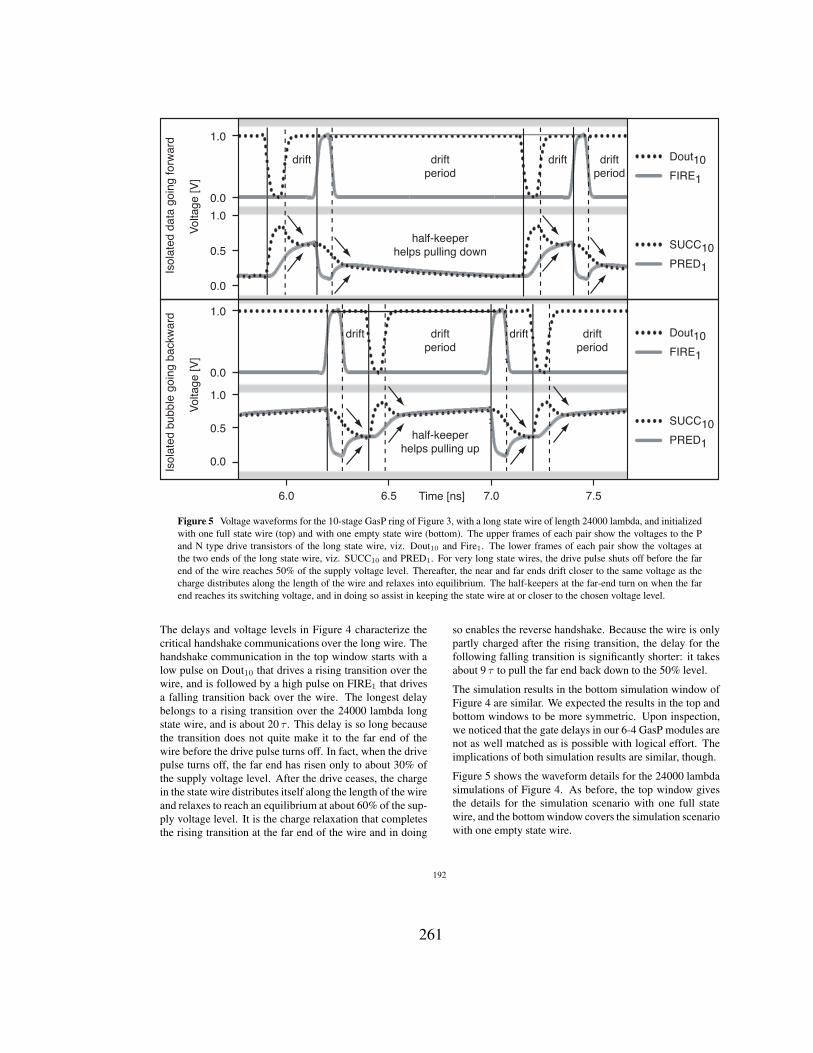
Vol
tage
[V]
Vol
tage
[V]
Isol
ated
dat
a go
ing
forw
ard
Isol
ated
bub
ble
goin
g ba
ckw
ard 1.0
1.0
1.0
0.0
0.0
0.0
0.0
1.0
0.5
0.5
driftperiod
drift
driftperiod
drift
driftperiod
drift
driftperiod
drift
half-keeperhelps pulling down
half-keeperhelps pulling up
Dout10FIRE1
SUCC10PRED1
Dout10FIRE1
SUCC10PRED1
Time [ns]6.0 6.5 7.0 7.5
Figure 5 Voltage waveforms for the 10-stage GasP ring of Figure 3, with a long state wire of length 24000 lambda, and initializedwith one full state wire (top) and with one empty state wire (bottom). The upper frames of each pair show the voltages to the Pand N type drive transistors of the long state wire, viz. Dout10 and Fire1. The lower frames of each pair show the voltages atthe two ends of the long state wire, viz. SUCC10 and PRED1. For very long state wires, the drive pulse shuts off before the farend of the wire reaches 50% of the supply voltage level. Thereafter, the near and far ends drift closer to the same voltage as thecharge distributes along the length of the wire and relaxes into equilibrium. The half-keepers at the far-end turn on when the farend reaches its switching voltage, and in doing so assist in keeping the state wire at or closer to the chosen voltage level.
The delays and voltage levels in Figure 4 characterize thecritical handshake communications over the long wire. Thehandshake communication in the top window starts with alow pulse on Dout10 that drives a rising transition over thewire, and is followed by a high pulse on FIRE1 that drivesa falling transition back over the wire. The longest delaybelongs to a rising transition over the 24000 lambda longstate wire, and is about 20 τ . This delay is so long becausethe transition does not quite make it to the far end of thewire before the drive pulse turns off. In fact, when the drivepulse turns off, the far end has risen only to about 30% ofthe supply voltage level. After the drive ceases, the chargein the state wire distributes itself along the length of the wireand relaxes to reach an equilibrium at about 60% of the sup-ply voltage level. It is the charge relaxation that completesthe rising transition at the far end of the wire and in doing
so enables the reverse handshake. Because the wire is onlypartly charged after the rising transition, the delay for thefollowing falling transition is significantly shorter: it takesabout 9 τ to pull the far end back down to the 50% level.
The simulation results in the bottom simulation window ofFigure 4 are similar. We expected the results in the top andbottom windows to be more symmetric. Upon inspection,we noticed that the gate delays in our 6-4 GasP modules arenot as well matched as is possible with logical effort. Theimplications of both simulation results are similar, though.
Figure 5 shows the waveform details for the 24000 lambdasimulations of Figure 4. As before, the top window givesthe details for the simulation scenario with one full statewire, and the bottom window covers the simulation scenariowith one empty state wire.
192
261
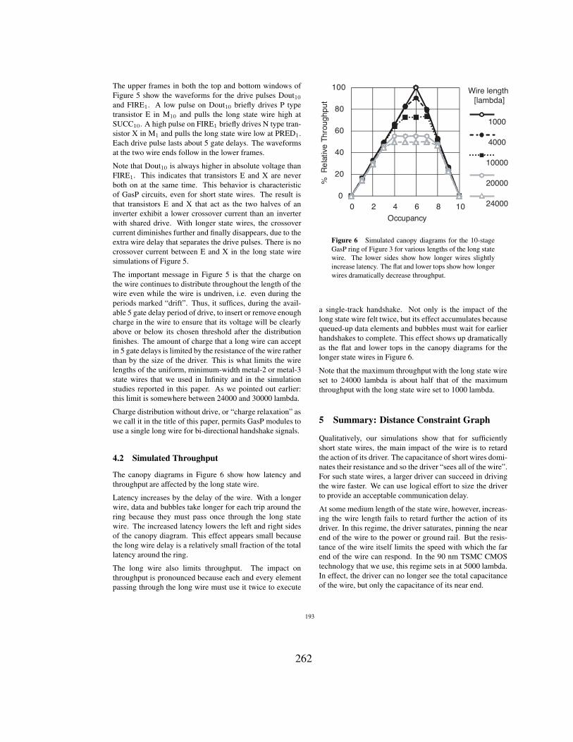
The upper frames in both the top and bottom windows ofFigure 5 show the waveforms for the drive pulses Dout10and FIRE1. A low pulse on Dout10 briefly drives P typetransistor E in M10 and pulls the long state wire high atSUCC10. A high pulse on FIRE1 briefly drives N type tran-sistor X in M1 and pulls the long state wire low at PRED1.Each drive pulse lasts about 5 gate delays. The waveformsat the two wire ends follow in the lower frames.
Note that Dout10 is always higher in absolute voltage thanFIRE1. This indicates that transistors E and X are neverboth on at the same time. This behavior is characteristicof GasP circuits, even for short state wires. The result isthat transistors E and X that act as the two halves of aninverter exhibit a lower crossover current than an inverterwith shared drive. With longer state wires, the crossovercurrent diminishes further and finally disappears, due to theextra wire delay that separates the drive pulses. There is nocrossover current between E and X in the long state wiresimulations of Figure 5.
The important message in Figure 5 is that the charge onthe wire continues to distribute throughout the length of thewire even while the wire is undriven, i.e. even during theperiods marked “drift”. Thus, it suffices, during the avail-able 5 gate delay period of drive, to insert or remove enoughcharge in the wire to ensure that its voltage will be clearlyabove or below its chosen threshold after the distributionfinishes. The amount of charge that a long wire can acceptin 5 gate delays is limited by the resistance of the wire ratherthan by the size of the driver. This is what limits the wirelengths of the uniform, minimum-width metal-2 or metal-3state wires that we used in Infinity and in the simulationstudies reported in this paper. As we pointed out earlier:this limit is somewhere between 24000 and 30000 lambda.
Charge distribution without drive, or “charge relaxation” aswe call it in the title of this paper, permits GasP modules touse a single long wire for bi-directional handshake signals.
4.2 Simulated Throughput
The canopy diagrams in Figure 6 show how latency andthroughput are affected by the long state wire.
Latency increases by the delay of the wire. With a longerwire, data and bubbles take longer for each trip around thering because they must pass once through the long statewire. The increased latency lowers the left and right sidesof the canopy diagram. This effect appears small becausethe long wire delay is a relatively small fraction of the totallatency around the ring.
The long wire also limits throughput. The impact onthroughput is pronounced because each and every elementpassing through the long wire must use it twice to execute
Wire length [lambda]
24000
20000
10000
4000
1000
% R
ela
tive
Thro
ughp
ut
Occupancy
0
20
40
60
80
100
0 2 4 6 8 10
Figure 6 Simulated canopy diagrams for the 10-stageGasP ring of Figure 3 for various lengths of the long statewire. The lower sides show how longer wires slightlyincrease latency. The flat and lower tops show how longerwires dramatically decrease throughput.
a single-track handshake. Not only is the impact of thelong state wire felt twice, but its effect accumulates becausequeued-up data elements and bubbles must wait for earlierhandshakes to complete. This effect shows up dramaticallyas the flat and lower tops in the canopy diagrams for thelonger state wires in Figure 6.
Note that the maximum throughput with the long state wireset to 24000 lambda is about half that of the maximumthroughput with the long state wire set to 1000 lambda.
5 Summary: Distance Constraint Graph
Qualitatively, our simulations show that for sufficientlyshort state wires, the main impact of the wire is to retardthe action of its driver. The capacitance of short wires domi-nates their resistance and so the driver “sees all of the wire”.For such state wires, a larger driver can succeed in drivingthe wire faster. We can use logical effort to size the driverto provide an acceptable communication delay.
At some medium length of the state wire, however, increas-ing the wire length fails to retard further the action of itsdriver. In this regime, the driver saturates, pinning the nearend of the wire to the power or ground rail. But the resis-tance of the wire itself limits the speed with which the farend of the wire can respond. In the 90 nm TSMC CMOStechnology that we use, this regime sets in at 5000 lambda.In effect, the driver can no longer see the total capacitanceof the wire, but only the capacitance of its near end.
193
262
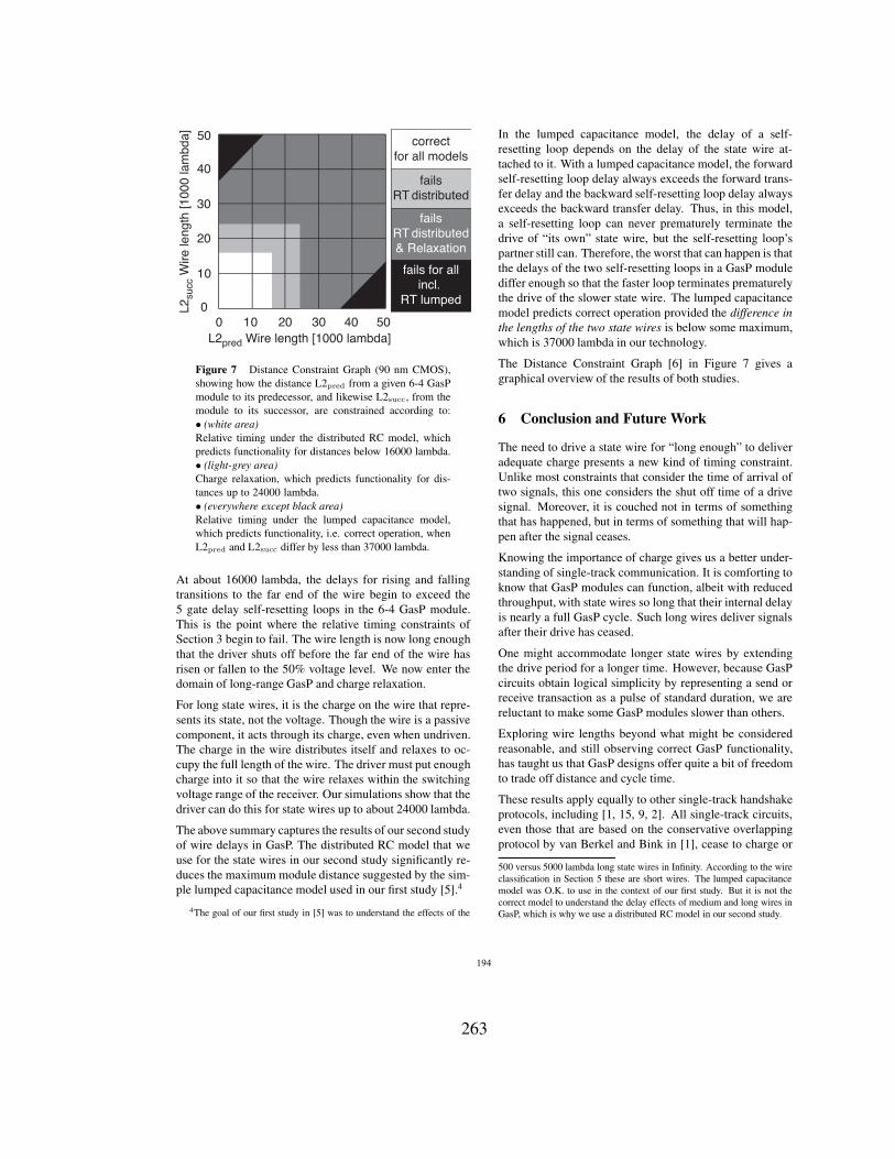
L2pred Wire length [1000 lambda]
L2su
cc W
ire le
ngth
[100
0 la
mbd
a]
0 10 20 30 40 500
10
20
30
40
50 correctfor all models
failsRT distributed
fails for allincl.
RT lumped
failsRT distributed& Relaxation
Figure 7 Distance Constraint Graph (90 nm CMOS),showing how the distance L2pred from a given 6-4 GasPmodule to its predecessor, and likewise L2succ, from themodule to its successor, are constrained according to:• (white area)Relative timing under the distributed RC model, whichpredicts functionality for distances below 16000 lambda.• (light-grey area)Charge relaxation, which predicts functionality for dis-tances up to 24000 lambda.• (everywhere except black area)Relative timing under the lumped capacitance model,which predicts functionality, i.e. correct operation, whenL2pred and L2succ differ by less than 37000 lambda.
At about 16000 lambda, the delays for rising and fallingtransitions to the far end of the wire begin to exceed the5 gate delay self-resetting loops in the 6-4 GasP module.This is the point where the relative timing constraints ofSection 3 begin to fail. The wire length is now long enoughthat the driver shuts off before the far end of the wire hasrisen or fallen to the 50% voltage level. We now enter thedomain of long-range GasP and charge relaxation.
For long state wires, it is the charge on the wire that repre-sents its state, not the voltage. Though the wire is a passivecomponent, it acts through its charge, even when undriven.The charge in the wire distributes itself and relaxes to oc-cupy the full length of the wire. The driver must put enoughcharge into it so that the wire relaxes within the switchingvoltage range of the receiver. Our simulations show that thedriver can do this for state wires up to about 24000 lambda.
The above summary captures the results of our second studyof wire delays in GasP. The distributed RC model that weuse for the state wires in our second study significantly re-duces the maximum module distance suggested by the sim-ple lumped capacitance model used in our first study [5].4
4The goal of our first study in [5] was to understand the effects of the
In the lumped capacitance model, the delay of a self-resetting loop depends on the delay of the state wire at-tached to it. With a lumped capacitance model, the forwardself-resetting loop delay always exceeds the forward trans-fer delay and the backward self-resetting loop delay alwaysexceeds the backward transfer delay. Thus, in this model,a self-resetting loop can never prematurely terminate thedrive of “its own” state wire, but the self-resetting loop’spartner still can. Therefore, the worst that can happen is thatthe delays of the two self-resetting loops in a GasP modulediffer enough so that the faster loop terminates prematurelythe drive of the slower state wire. The lumped capacitancemodel predicts correct operation provided the difference inthe lengths of the two state wires is below some maximum,which is 37000 lambda in our technology.
The Distance Constraint Graph [6] in Figure 7 gives agraphical overview of the results of both studies.
6 Conclusion and Future Work
The need to drive a state wire for “long enough” to deliveradequate charge presents a new kind of timing constraint.Unlike most constraints that consider the time of arrival oftwo signals, this one considers the shut off time of a drivesignal. Moreover, it is couched not in terms of somethingthat has happened, but in terms of something that will hap-pen after the signal ceases.
Knowing the importance of charge gives us a better under-standing of single-track communication. It is comforting toknow that GasP modules can function, albeit with reducedthroughput, with state wires so long that their internal delayis nearly a full GasP cycle. Such long wires deliver signalsafter their drive has ceased.
One might accommodate longer state wires by extendingthe drive period for a longer time. However, because GasPcircuits obtain logical simplicity by representing a send orreceive transaction as a pulse of standard duration, we arereluctant to make some GasP modules slower than others.
Exploring wire lengths beyond what might be consideredreasonable, and still observing correct GasP functionality,has taught us that GasP designs offer quite a bit of freedomto trade off distance and cycle time.
These results apply equally to other single-track handshakeprotocols, including [1, 15, 9, 2]. All single-track circuits,even those that are based on the conservative overlappingprotocol by van Berkel and Bink in [1], cease to charge or
500 versus 5000 lambda long state wires in Infinity. According to the wireclassification in Section 5 these are short wires. The lumped capacitancemodel was O.K. to use in the context of our first study. But it is not thecorrect model to understand the delay effects of medium and long wires inGasP, which is why we use a distributed RC model in our second study.
194
263
discharge the wire, or wires in case of [9, 2], based onlyon information available at the near end. The present studyextends the operational analysis available for single-tracksignaling beyond the lumped capacitance model.
We are currently investigating how to add long wires intothe logical effort models for logic with interconnect [7],how to support them in our timing analysis tools [4], andhow to engineer them to minimize the loss in latency andthroughput [8].
Perhaps the most important implication of this study is thatone can engineer the wires! Indeed, in the current era of cir-cuit technology where the properties of wires dominate de-lay as well as power and area, one should engineer the wiresas well as the transistors. For example, a 50% increase inthe width and spacing allocated for a 6-4 GasP state wirecan improve its delay by a factor of two at an area cost ofless than 1% for a single-rail 64-bit datapath. It is wise toallocate more space to a single-track state wire that makesmultiple transitions per transaction than to a bundled datawire that makes only one. Improvement of selected statewires may further optimize the design at locations where thebi-directional single-track signaling would otherwise fail tokeep up with the uni-directional data, as for example shownin [3]. Understanding how to use wire engineering to im-prove distance and cycle time permits us to reason aboutand optimize the insertion and placement of GasP repeaters.
We hope soon to build a next test chip to confirm that realGasP circuits can indeed operate with long state wires. Thischip will also explore how engineering the wires can im-prove performance. We hope that measurements from sucha chip will shed light on the speed, the power demand, andthe reliability of long-range GasP circuits.
Acknowledgments We gratefully acknowledge Jon Lexaufor (running)∗ our 90 nm simulations. Sun Microsystemspaid for the design, fabrication and testing of Infinity, andalso sponsored the present work through a generous grantto the Portland State University Foundation.
References[1] K. v. Berkel and A. Bink. Single-Track Handshake Signaling
with Application to Micropipelines and Handshake Circuits.In Proc. Advanced Research in Asynchronous Circuits andSystems (ASYNC), pages 122–133, 1996.
[2] M. Ferretti and P. Beerel. High Performance Asyn-chronous Design Using Single-Track Full-Buffer StandardCells. IEEE Journal of Solid-State Circuits, 41(6):1444–1454, 2006.
[3] R. Ho, J. Gainsley, and R. Drost. Long Wires and Asyn-chronous Control. In Proc. IEEE International Sympo-sium on Asynchronous Circuits and Systems (ASYNC), pages240–249, 2004.
[4] P. Joshi. Static Timing Analysis of GasP. Master of Sciencethesis, Electrical Engineering, Faculty of the USC ViterbiSchool of Engineering, University of Southern California,December 2008.
[5] P. Joshi, P. Beerel, M. Roncken, and I. Sutherland. Tim-ing Verification of GasP Asynchronous Circuits: PredictedDelay Variations Observed by Experiment. In D. Dams,U. Hannemann, M. Steffen (Eds.): Willem-Paul de RoeverFestschrift, LNCS 5930, pages 260–276. Springer-VerlagBerlin Heidelberg, 2010.
[6] S. Mettala Gilla. Distance Constraint Graph: A GraphicalRepresentation for 6-4 GasP showing how Relative Tim-ings constrain the Module Distances. Technical Report,ARC2009-smg01, Asynchronous Research Center, PortlandState University, September 2009.
[7] A. Morgenshtein, E. Friedman, R. Ginosar, and A. Kolodny.Timing Optimization in Logic with Interconnect. In Proc.International Workshop on System Level Interconnect Pre-diction (SLIP), pages 19–26, 2008.
[8] F. Mu and C. Svensson. Analysis and Optimization of aUniform Long Wire and Driver. IEEE Transactions on Cir-cuits and Systems I: Fundamental Theory and Applications,46(9):1086–1100, 1999.
[9] M. Nystrom, E. Ou, and A. Martin. An Eight-Bit DividerImplemented with Asynchronous Pulse Logic. In Proc.IEEE International Symposium on Asynchronous Circuitsand Systems (ASYNC), pages 229–239, 2004.
[10] A. Peeters and K. van Berkel. Single-rail Handshake Cir-cuits. In Proc. Asynchronous Design Methodologies, pages53–62, 1995.
[11] J. Rabaey, A. Chandrakasan, and B. Nikolic. Digital Inte-grated Circuits: A Design Perspective. Prentice-Hall, 2003.
[12] K. Stevens, R. Ginosar, and S. Rotem. Relative Timing. InProc. IEEE International Symposium on Advanced Researchin Asynchronous Circuits and Systems (ASYNC), pages 208–218, 1999.
[13] K. Stevens, R. Ginosar, and S. Rotem. Relative Timing.IEEE Transactions on Very Large Scale Integration (VLSI)Systems, 11(1):129–140, 2003.
[14] I. Sutherland. A Six-Four GasP Tutorial. Technical Report,UCIES2007-is49 at http://fleet.cs.berkeley.edu/docs, 2007.
[15] I. Sutherland and S. Fairbanks. GasP: A Minimal FIFOControl. In Proc. IEEE International Symposium on Asyn-chronous Circuits and Systems (ASYNC), pages 46–53,2001.
[16] I. Sutherland, B. Sproull, and D. Harris. Logical Effort: De-signing Fast CMOS Circuits. Morgan Kaufmann, San Fran-cisco, 1999.
[17] N. Weste and D. Harris. CMOS VLSI Design: A Circuitsand Systems Perspective. Addison-Wesley, 2005.
195
264
Appendix P
BONUS MATERIAL: THESIS POWERPOINT PRESENTATION
265
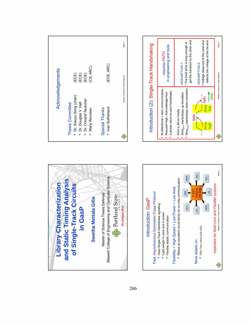
Libr
ary
Cha
ract
eriz
atio
n an
d St
atic
Tim
ing
Ana
lysi
s of
Sin
gle-
Trac
k C
ircui
tsin
Gas
PSw
etha
Met
tala
Gill
a
Mas
ter o
f Sci
ence
The
sis
Def
ense
Mas
eeh
Col
lege
of E
ngin
eerin
g an
d C
ompu
ter S
cien
ce
29O
ctob
er20
10
Ack
now
ledg
emen
ts
Thes
is C
omm
ittee
•D
r. Xi
aoyu
Son
g (c
hair)
(EC
E)
•D
r. D
ougl
as V
. Hal
l (E
CE
)•
Dr.
Chr
isto
f Teu
sche
r (E
CE
)•
Mar
lyR
onck
en
(CS
, AR
C)
Spe
cial
Tha
nks
•Iv
an S
uthe
rland
(E
CE
, AR
C)
Mas
ter o
f Sci
ence
The
sis
Def
ense
Slid
e 2
Intro
duct
ion:
Gas
PFa
stA
sync
hron
ous
Sym
met
ric P
ulse
Pro
toco
l•
Use
s S
ingl
e-Tr
ack
Han
dsha
ke s
igna
ling
•Li
ght-w
eigh
t in
area
and
in p
ower
•Fl
exib
le e
last
ic c
omm
unic
atio
n
Flex
ibili
ty +
Hig
h S
peed
+ L
ow P
ower
+ L
ow A
rea
•M
akes
an
exce
llent
circ
uit f
amily
for o
n-ch
ip c
omm
unic
atio
n
Mor
e de
tails
on:
•ht
tp://
arc.
cecs
.pdx
.edu
Impo
rtant
for M
ulti-
core
and
Par
alle
l sys
tem
s
ME
M SR
T
MU
LI/O
ME
M
DIVA
LUA
DD
FLE
ET
Net
wor
kO
n C
hip
Mas
ter o
f Sci
ence
The
sis
Def
ense
Slid
e 3
Intro
duct
ion
(2):
Sin
gle-
Trac
k H
ands
haki
ng
Mas
ter o
f Sci
ence
The
sis
Def
ense
•B
i-dire
ctio
nal 1
-wire
com
mun
icat
ion
•R
eque
st=h
igh,
Ack
now
ledg
e=lo
w•
2-ph
ase
retu
rn-to
-zer
o ha
ndsh
ake
•W
ire is
driv
en b
riefly
•W
ireen
d1st
arts
/sto
ps u
p-tra
nsiti
on•
Wire
end2
star
ts/s
tops
dow
n-tra
nsiti
onA
SS
UM
PTI
ON
-1:
•The
brie
f driv
e is
long
eno
ugh
to
get t
he tr
ansi
tion
to th
e ot
her e
nd
AS
SU
MP
TIO
N-2
:•V
olta
ge o
bser
ved
at th
e ne
ar-e
ndre
flect
s th
e vo
ltage
at t
he fa
r-end
Slid
e 4
driv
ehi
ghdr
ive
low
time
faith
faith
requ
ires
FAIT
Hin
eng
inee
ring
and
tool
s
266
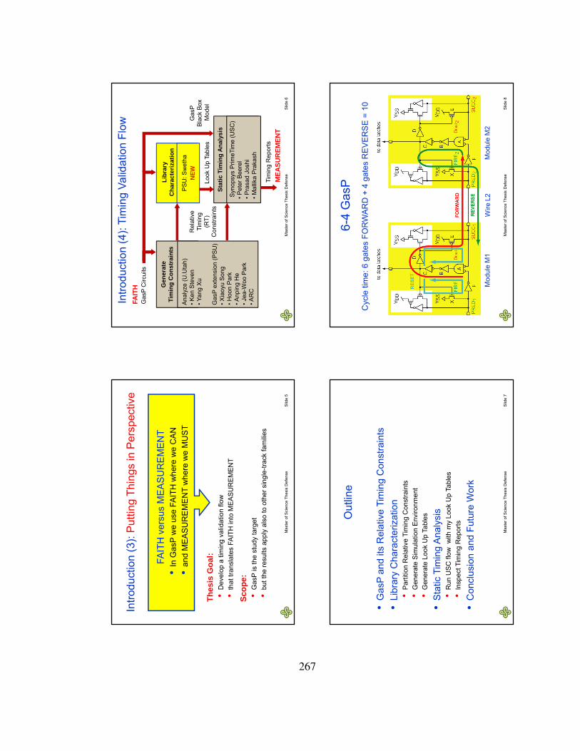
Intro
duct
ion
(3):
Put
ting
Thin
gs in
Per
spec
tive
FAIT
H v
ersu
s M
EA
SU
RE
ME
NT
•In
Gas
Pw
e us
e FA
ITH
whe
re w
e C
AN
•a
nd M
EA
SU
RE
ME
NT
whe
re w
e M
US
T
Thes
is G
oal:
•D
evel
op a
tim
ing
valid
atio
n flo
w•
that
tran
slat
es F
AIT
H in
to M
EA
SU
RE
ME
NT
Scop
e:•
Gas
Pis
the
stud
y ta
rget
•bu
t the
resu
lts a
pply
als
o to
oth
er s
ingl
e-tra
ck fa
milie
s
Mas
ter o
f Sci
ence
The
sis
Def
ense
Slid
e 5
Intro
duct
ion
(4):
Tim
ing
Valid
atio
n Fl
ow
PS
U: S
wet
haN
EW
Libr
ary
Cha
ract
eriz
atio
n
Look
Up
Tabl
es
MEA
SUR
EMEN
T
FAIT
H
Ana
lyze
(U.U
tah)
•Ken
Ste
ven
•Yan
g X
u
Gas
P ex
tens
ion
(PS
U)
•X
iaoy
u S
ong
•Hoo
n P
ark
•Anp
ing
He
•Jea
-Woo
Par
k•A
RC
Gen
erat
e Ti
min
g C
onst
rain
ts
Gas
P C
ircui
ts
Rel
ativ
e Ti
min
g(R
T)C
onst
rain
ts
Stat
ic T
imin
g An
alys
is
Syn
opsy
s P
rimeT
ime
(US
C)
•Pet
er B
eere
l •P
rasa
d Jo
shi
•Mal
lika
Pra
kash
Gas
P B
lack
Box
M
odel
Tim
ing
Rep
orts
Mas
ter o
f Sci
ence
The
sis
Def
ense
Slid
e 6
Out
line
•G
asP
and
its R
elat
ive
Tim
ing
Con
stra
ints
•Li
brar
y C
hara
cter
izat
ion
•P
artit
ion
Rel
ativ
e Ti
min
g C
onst
rain
ts•
Gen
erat
e S
imul
atio
n E
nviro
nmen
t •
Gen
erat
e Lo
ok U
p Ta
bles
•S
tatic
Tim
ing
Ana
lysi
s•
Run
US
C fl
ow w
ith m
y Lo
ok U
p Ta
bles
•In
spec
t Tim
ing
Rep
orts
•C
oncl
usio
n an
d Fu
ture
Wor
k
Mas
ter o
f Sci
ence
The
sis
Def
ense
Slid
e 7
6-4
Gas
P
Mod
ule
M1
Mod
ule
M2
Cyc
le ti
me:
6 g
ates
FO
RW
AR
D +
4 g
ates
RE
VE
RS
E =
10
Wire
L2
Mas
ter o
f Sci
ence
The
sis
Def
ense
Slid
e 8
267
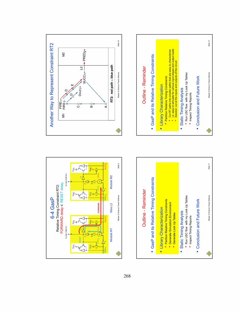
6-4
Gas
P
Mod
ule
M1
Mod
ule
M2
Rel
ativ
e Ti
min
g C
onst
rain
t RT2
: FO
RW
AR
D d
elay
≤ R
ES
ET
dela
y
Wire
L2
Mas
ter o
f Sci
ence
The
sis
Def
ense
Slid
e 9
Ano
ther
Way
to R
epre
sent
Con
stra
int R
T2
Mas
ter o
f Sci
ence
The
sis
Def
ense
Slid
e 10
•G
asP
and
its R
elat
ive
Tim
ing
Con
stra
ints
•Li
brar
y C
hara
cter
izat
ion
•P
artit
ion
Rel
ativ
e Ti
min
g C
onst
rain
ts•
Gen
erat
e S
imul
atio
n E
nviro
nmen
t •
Gen
erat
e Lo
ok U
p Ta
bles
•S
tatic
Tim
ing
Ana
lysi
s•
Run
US
C fl
ow w
ith m
y Lo
ok U
p Ta
bles
•In
spec
t Tim
ing
Rep
orts
•C
oncl
usio
n an
d Fu
ture
Wor
k
Out
line
-Rem
inde
r
Mas
ter o
f Sci
ence
The
sis
Def
ense
Slid
e 11
•G
asP
and
its R
elat
ive
Tim
ing
Con
stra
ints
•Li
brar
y C
hara
cter
izat
ion
•P
artit
ion
Rel
ativ
e Ti
min
g C
onst
rain
ts•
Gen
erat
e S
imul
atio
n E
nviro
nmen
t •
Gen
erat
e Lo
ok U
p Ta
bles
•S
tatic
Tim
ing
Ana
lysi
s•
Run
US
C fl
ow w
ith m
y Lo
ok U
p Ta
bles
•In
spec
t Tim
ing
Rep
orts
•C
oncl
usio
n an
d Fu
ture
Wor
k
•C
ut R
T pa
ths
into
sm
alle
r pat
hs th
at a
re e
asy
to c
hara
cter
ize
•i.e
. eas
y to
sim
ulat
e fo
r var
ious
inpu
t slo
pes
and
outp
ut lo
ads
•S
olut
ion:
cut
at t
he in
puts
and
out
puts
of t
he c
ircui
t
Out
line
-Rem
inde
r
Mas
ter o
f Sci
ence
The
sis
Def
ense
Slid
e 12
268
Par
titio
n R
T2 c
onst
rain
tC
ut re
d pa
th a
t SU
CC
1+
Cut
blu
e pa
th a
t S
UC
C1+
FIR
E 1-
Mas
ter o
f Sci
ence
The
sis
Def
ense
Slid
e 13
•G
asP
and
its R
elat
ive
Tim
ing
Con
stra
ints
•Li
brar
y C
hara
cter
izat
ion
•P
artit
ion
Rel
ativ
e Ti
min
g C
onst
rain
ts•
Gen
erat
e S
imul
atio
n E
nviro
nmen
t •
Gen
erat
e Lo
ok U
p Ta
bles
•S
tatic
Tim
ing
Ana
lysi
s•
Run
US
C fl
ow w
ith m
y Lo
ok U
p Ta
bles
•In
spec
t Tim
ing
Rep
orts
•C
oncl
usio
n an
d Fu
ture
Wor
k
Out
line
-Rem
inde
r
Mas
ter o
f Sci
ence
The
sis
Def
ense
Slid
e 14
•G
asP
and
its R
elat
ive
Tim
ing
Con
stra
ints
•Li
brar
y C
hara
cter
izat
ion
•P
artit
ion
Rel
ativ
e Ti
min
g C
onst
rain
ts•
Gen
erat
e S
imul
atio
n E
nviro
nmen
t •
Gen
erat
e Lo
ok U
p Ta
bles
•S
tatic
Tim
ing
Ana
lysi
s•
Run
US
C fl
ow w
ith m
y Lo
ok U
p Ta
bles
•In
spec
t Tim
ing
Rep
orts
•C
oncl
usio
n an
d Fu
ture
Wor
k
•C
ut th
e ci
rcui
t int
o sm
alle
r sub
-circ
uits
that
fit t
he s
ub-p
aths
•A
dd c
ircui
try to
sim
ulat
e m
in-m
ax d
elay
s an
d re
set s
ingl
e-tra
ck w
ires
•E
mbe
d in
a fi
nal s
etup
for s
wee
ping
inpu
t slo
pes
and
outp
ut lo
ads
Out
line
-Rem
inde
r
Mas
ter o
f Sci
ence
The
sis
Def
ense
Slid
e 15
VCC
S
VCVS
Par
titio
n th
e 6-
4 G
asP
circ
uit f
or R
T2
Mas
ter o
f Sci
ence
The
sis
Def
ense
Slid
e 16
269
Wha
t:•
Min
imiz
e th
e (B
LUE
) Res
et L
oop
Del
ay•
by m
inim
izin
g th
e de
lay
of N
OR
-func
tion
A go
ing
dow
n
Firs
t Circ
uit E
nhan
cem
ent f
or R
T2
Mas
ter o
f Sci
ence
The
sis
Def
ense
Slid
e 17
00.5
1
-2-1
01
2
Output Delay after 1stInputtout-min (tin1, tin2)
Inp
ut
Sep
arat
ion
Tim
e =
(tin
2-
t in1
)/2
t in2
too
late
t in1
too
late
t in1
first
t in2
first
Min
imum
Firs
t Circ
uit E
nhan
cem
ent f
or R
T2 -
cont
inue
d
Mas
ter o
f Sci
ence
The
sis
Def
ense
Slid
e 18
How
: by
usi
ng a
“dem
on in
a b
ox”
Volta
geC
ontro
lled
Volta
geSo
urce
•Th
at c
opie
s V
(SU
CC
1) to
V(n
PR
ED
1)w
ithou
t ext
ra d
elay
or l
oad
The
VC
VS
in th
is p
ictu
re•
Min
imiz
es th
e fa
lling
dela
y of
gat
e A
•an
d th
us th
e de
lay
of R
T2 s
ub-p
ath
LUTb
lue:
SU
CC
1+FI
RE
1-
Mas
ter o
f Sci
ence
The
sis
Def
ense
Slid
e 19
Sec
ond
Circ
uit E
nhan
cem
ent f
or R
T2
Wha
t: •M
odul
e M
1 ca
n on
ly ra
ise
SU
CC
1
beca
use
it’s
a si
ngle
-trac
k si
gnal
•So:
SU
CC
1m
ust b
e re
-initi
aliz
edbe
fore
the
next
sim
ulat
ion
cycl
e
How
: ano
ther
“dem
on in
a b
ox”
Volta
geC
ontro
lled
Cur
rent
Sour
ce•T
hat u
ses
as c
ompl
etio
n pu
lse
sign
alFI
RE
_CS
1to
rese
t SU
CC
1
•by
trans
latin
g th
e su
rplu
s vo
ltage
on S
UC
C1
into
a d
rain
cur
rent
•with
out d
elay
ing
or lo
adin
g S
UC
C1+
Rel
atio
nshi
p FI
RE
_CS
1to
FIR
E1
and
SU
CC
1
•R
eset
: SU
CC
1fa
lls a
fter F
IRE
1fa
lls a
nd b
efor
e FI
RE
1ris
es•
Mea
sure
men
t: S
UC
C1
rises
with
in th
e FI
RE
1hi
gh-p
ulse
win
dow
•M
utua
l exc
lusi
on: V
CC
S d
rain
cur
rent
= 0
A du
ring
the
FIR
E1
high
-pul
se
Mas
ter o
f Sci
ence
The
sis
Def
ense
Slid
e 20
dem
onin
act
ion
270
Fina
l Sim
ulat
ion
Set
up
•S
wee
p:Tr
ash
size
wid
T (d
river
circ
uitry
) and
Loa
d si
ze w
id2
(load
circ
uitry
)•
Mea
sure
: Tim
ing
and
Volta
ge c
hang
es o
n in
[1] a
nd o
ut[1
]•
Res
ult:
(wid
T x
wid
2)
slop
e(in
[1])
, del
ay(in
[1] t
o ou
t[1]),
slo
pe(o
ut[1
])
Mas
ter o
f Sci
ence
The
sis
Def
ense
Slid
e 21
… a
nd th
e Lo
ok U
p Ta
ble
that
it g
ener
ates
Mas
ter o
f Sci
ence
The
sis
Def
ense
Slid
e 22
•S
tore
s: (I
nput
Slo
pe x
Out
put L
oad)
de
lay(
in[1
] to
out[1
]), s
lope
(out
[1])
LUTb
lue:
SUC
C1+
FIR
E1-
dela
y(12
.24p
s ,0
fF)=
35.
8 –(
((14
.2 –
12.2
4) /
(15.
1 –
14.2
)) x
(36
.3 –
35.8
)) =
34.
71 p
s
slop
e(12
.24p
s, 0
fF)=
8.
8 –(
((14
.2 –
12.2
4) /
(15.
1 –
14.2
)) x
(8.
6 –
8.8)
)
= 9
.24
ps
LUTb
lue:
SUC
C1+
FIR
E1-
Mas
ter o
f Sci
ence
The
sis
Def
ense
Slid
e 23
… is
use
d as
follo
ws
Land
scap
e G
raph
s fo
r the
Loo
k U
p Ta
ble
DE
LAY
land
scap
e(c
olor
dis
tinct
ion
ever
y 10
ps)
14.215
.116.321.4
01020304050607080
0.0
18.2
59.3
101.
414
2.8
185.
1
Delay [ps]
LU
Tb
lue:
SU
CC
+FIR
E-
0-10
10-2
020
-30
30-4
040
-50
50-6
060
-70
70-8
0
14.215
.116.321.4
051015202530354045
0.0
18.2
59.3
101.
414
2.8
185.
1
Output slope [ps]
LU
Tb
lue:
SU
CC
+FIR
E-
0-5
5-10
10-1
515
-20
20-2
5
Mas
ter o
f Sci
ence
The
sis
Def
ense
Slid
e 24
OU
TPU
T S
LOP
E la
ndsc
ape
(col
or d
istin
ctio
n ev
ery
5 ps
)
BO
TH a
re v
ery
amen
able
to li
near
app
roxi
mat
ion
tech
niqu
es
271
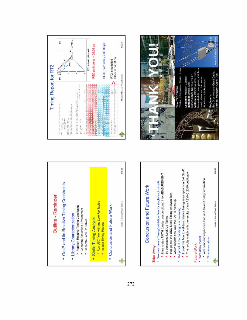
•G
asP
and
its R
elat
ive
Tim
ing
Con
stra
ints
•Li
brar
y C
hara
cter
izat
ion
•P
artit
ion
Rel
ativ
e Ti
min
g C
onst
rain
ts•
Gen
erat
e S
imul
atio
n E
nviro
nmen
t •
Gen
erat
e Lo
ok U
p Ta
bles
•S
tatic
Tim
ing
Ana
lysi
s•
Run
US
C fl
ow w
ith m
y Lo
ok U
p Ta
bles
•In
spec
t Tim
ing
Rep
orts
•C
oncl
usio
n an
d Fu
ture
Wor
k
Out
line
-Rem
inde
r
Mas
ter o
f Sci
ence
The
sis
Def
ense
Slid
e 25
Tim
ing
Rep
ort f
or R
T2
Mas
ter o
f Sci
ence
The
sis
Def
ense
Slid
e 26
RE
D p
ath
dela
y =
26.3
6 ps
BLU
E p
ath
dela
y =
80.3
9 ps
RT2
is s
atis
fied
Sla
ck =
54.
03 p
s
Con
clus
ion
and
Futu
re W
ork
Take
-Aw
ay:
•W
e no
w h
ave
a Ti
min
g Va
lidat
ion
flow
for s
ingl
e-tra
ck c
ircui
ts•
It tra
nsla
tes
FAIT
H (d
esig
n as
sum
ptio
ns) i
nto
ME
AS
UR
EM
EN
T•
by g
ener
atin
g Lo
ok U
p Ta
bles
•
that
go
into
the
US
C S
tatic
Tim
ing
Ana
lysi
s flo
w•
whi
ch re
ports
how
wel
l the
FA
ITH
hol
ds u
p •
The
proo
f of t
he p
uddi
ng is
in th
e ea
ting
•I u
sed
this
flow
to v
alid
ate
rela
tive
timin
g as
sum
ptio
ns in
6-4
Gas
P•
The
resu
lts m
atch
with
the
resu
lts o
f my
AS
YNC
201
0 pu
blic
atio
n
Futu
re W
ork:
•W
ire d
elay
mod
el•
with
nea
r-end
cap
aciti
ve lo
ad a
nd fa
r-end
del
ay in
form
atio
n•
Flow
aut
omat
ion
Mas
ter o
f Sci
ence
The
sis
Def
ense
Slid
e 27
Title
: TEC
OTO
SHTE
nsio
n+
CO
mpr
essi
on+
TOrs
ion
+ S
Hea
r
Loca
tion:
Mas
eeh
Col
lege
Inst
alle
d: M
arch
200
6.D
imen
sion
s: 1
30' x
40'
x 4
0'.
Mat
eria
ls: S
tain
less
ste
el tr
uss,
la
min
ated
dic
hroi
c gl
ass,
sta
inle
ss
stee
l cab
les
and
hard
war
e.
Alu
min
um li
ght h
ousi
ngs.
Engi
neer
s:
Bob
Gru
mm
el a
nd G
rant
Dav
is.
Proj
ect M
anag
er:O
anh
Tran
.
Slid
e 28
THA
NK
YO
U!
Mas
ter o
f Sci
ence
The
sis
Def
ense
272
Recommended