1/8
Application Note
© 2020 ROHM Co., Ltd. No. 63AN147E Rev.0022020.12
Laser Diode for LiDAR
Laser Diode Drive Circuit Design Method and Spice Model ROHM offers laser diodes (LDs) for Light Detection and Ranging (LiDAR). This application note will introduce ROHM's LD line-
up and show how to design the drive circuits of ROHM LDs. In addition, ROHM provides an evaluation board and a Spice model
for evaluating LDs and will show how to use them and some important points.
1. The Lineup and Features of ROHM's Pulse LD
Pulse laser diodes are LDs that produce high optical output
power with short current application time (pulse width). In
recent years, many applications, such as distance
measurement, have emerged.
Many LDs are designed with continuous wave (CW) drives
that produce optical output from a few mW to several W.
When such LDs try to output higher optical output power than
a specific optical output power, even if the pulse width is
short, the optical cavity is damaged, and the optical output
cannot be generated.
However, pulse LDs are designed to produce high optical
output power with short pulse widths. The drive of the pulse
LD must be determined by the pulse width and duty cycle. In
order to achieve high optical output power, the duty cycle
must be very small. For example, a duty cycle of 0.05%
(100 µs per cycle, 50 ns pulse width) means that very short
pulse currents are repeatedly applied in the kHz range. The
applied current to the LDs is from several A to several tens of
A to produce high optical output power pulses.
The wavelength of pulse LDs is material-dependent, and
ROHM can offer 905 nm. 905 nm wavelength range is made
up of AlGaAs, a material with high reliability, high beam
quality and stable temperature characteristics. Pulse laser
diodes use a stack structure consisting of multiple light-
emitting layers to achieve high optical output power. ROHM's
three-layered stacks are used to achieve Up to 120 W optical
output can be provided.
ROHM's pulse LDs are characterized by a narrow
luminescence width and good wavelength temperature
dependence. Table.1 shows the emission images for the
optical output lineup. The narrower the luminescence width,
the higher the optical density, and the longer the distance
can be measured with the same optical output power. In
addition, the narrower the luminescence width, the smaller
the beam area can be when irradiating an object, which
enables a higher resolution LiDAR module to be used.
Table of contents
1. The Lineup and Features of ROHM’s Pulse LD ・・・・・・・・・・・・・・・・・・・・・・・・・・・・・ 1
2. LiDAR and ToF method ・・・・・・・・・・・・・・・・・・・・・・・・・・・・・・・・・・・・・・・・・・・・・・・・・・ 2
3. LD Drive Circuit Design Method ・・・・・・・・・・・・・・・・・・・・・・・・・・・・・・・・・・・・・・・・・・・ 3
4. Evaluation Board (Resonant Wave Circuit) ・・・・・・・・・・・・・・・・・・・・・・・・・・・・・・・・・・ 5
5. Evaluation Board (Square Wave Circuit) ・・・・・・・・・・・・・・・・・・・・・・・・・・・・・・・・・・・・ 6
6. Simulation Models and Demo Circuits ・・・・・・・・・・・・・・・・・・・・・・・・・・・・・・・・・・・・・ 7
7. References ・・・・・・・・・・・・・・・・・・・・・・・・・・・・・・・・・・・・・・・・・・・・・・・・・・・・・・・・・・・・ 8

2/8 © 2020 ROHM Co., Ltd. No. 63AN147E Rev.0022020.12
Laser Diode Drive Circuit Design Method and Spice Model Application Note
Table 1. Luminescent Images for Optical Output Lineup
Improving Signal to Noise (S/N) ratio in LiDAR's optical
system, put in a band-pass filter to cut other than required
wavelength range. The wavelength temperature dependence
of ROHM's pulse LDs have an outstanding wavelength
temperature dependence of 0.15 nm/°C. This makes it
possible to design a narrower wavelength range for the
band-pass filter to cut, thus improving the S/N ratio of LiDAR
modules.
2. LiDAR and ToF method LiDAR is an abbreviation for "Light Detection and Ranging"
and has been attracting attention in various fields such as
automobiles, robots, drones, surveillance cameras, etc. Time
of Flight (ToF) method is the most used distance
measurement method in LiDAR. In the ToF method, as
shown in Fig. 2-1, the distance is calculated by measuring
the time it takes for the light emitted from the light source to
be reflected by the object and returned to the detector (flight
time).
The distance between the light source and the object is
defined by the following equation, where d is the distance
between the light source and the object and tf is the time of
flight.
∙ ・・・(2-1)
c is the speed of light in above equation.
Fig. 2-1. Conceptual diagram of the Time of Flight(ToF)
method.
Higher optical output power is required to improve the
measuring distance. The farther away the distance is, the
lower the rate of return of the optical output power. That is
caused by light attenuation in the air. *1 For this reason,
higher optical output power is required to view objects over
long distances.
In order to improve the distance resolution, the pulse width
must be made shorter. When the pulse width is longer, the
light pulses received by the detector tend to overlap, making
it difficult to distinguish between two or more objects that are
close to each other. For this reason, shorter pulses are
required to improve distance accuracy. Shorter pulses can
also increase the maximum optical output power from an eye
safe standpoint.
The required distance resolution and distance range are
different for each application, as shown in Fig. 2-2.
Therefore, the required optical output power and pulse
widths are different for each application, and it is important to
select the right device and design the circuit for each
application.
Fig. 2-2. Assumed uses of the ToF method.
※ Optical output with a pulse width of 50 ns

3/8 © 2020 ROHM Co., Ltd. No. 63AN147E Rev.0022020.12
Laser Diode Drive Circuit Design Method and Spice Model Application Note
3. LD Drive Circuit Design Method To output high power with short pulses, not only the
selection of the LD, but also the design of the LD drive circuit
is important. There are various types of LD drive circuits, and
here we will discuss the current resonant circuits. Current-
resonant circuits are characterized by high optical output
power and short pulses.
The drive circuit is shown in Fig. 3-1. The main current
paths are the LD, the resonant capacitor Cr and the switching
element Q1. When Q1 is switched off, Cr is charged in the I1
path. The moment Q1 is turned on, current flows in the path
from Cr to I2, allowing light to be output from the LD. If you
don't add a resistor Rl to limit the current of I1, the current of
I2 will be small.
Due to the current in I2, reverse electric charge gradually
builds up in the Cr in the opposite direction. This electric
charge in the Cr causes the current to start flowing in the I3
path. At this time, if a diode Dp is not connected to the LDs,
the voltage is applied to the LDs, which may damage the
device. (In the resonant wave circuit shown in Fig. 3-1, the
LDs cannot be driven normally without the Dp because it also
serves as a charging path.) If vibration is not suppressed
while current is flowing through the I3 path, current will flow
through the I2 path again, which will generate unnecessary
optical output power. Normally, Q1 is turned off at the time
when the LDs move from I2 to I3, so the second and
subsequent currents are less likely to flow. However, even
when Q1 is turned off, current flows through the drain-source
capacitance of Q1, so the higher the optical output, the more
likely it is that unwanted optical output is generated. The
second and subsequent optical output can cause false
positives, so it is important to suppress vibrations while the
current flows back. For this reason, RD is connected in series
with the Dp to suppress the vibration, and when the Cr charge
is removed, it is recharged again through I1.
Fig. 3-1. Current resonance circuit diagram.
Because the current path of the I2 shown in Fig. 3-1 is a free
oscillation circuit of LCR, the current can be defined by the
following equation.
sin ・・・(3-1)
Here.
・・・(3-2)
!" ・・・(3-3)
and R is the sum of the on-resistance of Q1, the resistance
component (VFLD/I2) due to the forward drop voltage VFLD of
LD, the ESR of Cr, and the wiring resistance of the main
current path. Vin is the input voltage and Lr is the parasitic
inductance of the current path of I2.
Here, Q1 is assumed to be an ideal switch.
From equation (3-1), the resonant period Tres is expressed by
the following equation.
#$%& ' ・・・(3-4)
Since the maximum current I2max is the current at 1/4 cycle
from the beginning of the current flow, I2max can be expressed
by the equation (3-5). The larger this I2max, the greater the
optical output power can be.
()*
+,-. sin/-.0 ・・・(3-5)
The pulse width Tp can be expressed by the equation (3-6).
#1 /-.2 '
2 ・・・(3-6)

4/8 © 2020 ROHM Co., Ltd. No. 63AN147E Rev.0022020.12
Laser Diode Drive Circuit Design Method and Spice Model Application Note
Using these equations, Fig. 3-2 shows the relationship
between the Tp and I2max for Cr and Lr. (Fig. 3-2 shows the
results for Vin=80 V, R=0.3 Ω.) Fig. 3-2 shows that the Tp can
be shortened by reducing the Lr, while improving the I2max.
Although the Tp can be shortened by reducing the Cr, the
I2max decreases at the same time, so that the selection of a
suitable Cr value for the application is important.
Fig. 3-2. Relationship between (a) maximum current I2max and
(b) pulse width Tp for resonant capacitor Cr and parasitic
inductance Lr.
Impact of layout design Lr value varies greatly depending on the circuit layout
design, so care must be taken when designing. In general,
the smaller the area of the closed loop in the current path,
the smaller the inductance. Therefore, by reducing the area
of the current loop of the I2 shown Fig 3-1, the value of Lr can
be reduced. To reduce the area of the current path loops, Lr
can be reduced by forming loops in the thickness direction of
the substrate rather than forming the loops in a planar shape.
*2 In addition to the main current loop, it is also important to
reduce the inductance Lg between the gate and source. If the
Lg is large, the gate surge voltage becomes large and
exceeds the breakdown voltage of the device, so it is
important to design the gate-source loop as small as possible
so that the Lg is as small as possible.
Effect of LD As shown in Equation (3-1), it is important to select an
element with a small VFLD to increase the output power. Also,
the higher the quantum efficiency of the device, the higher
the output power can be when the same current is applied.
ROHM's datasheet shows the output power with a pulse
width of 50 ns, but the optical output power varies depending
on the pulse width. In general, the shorter the pulse width,
the less affected by heat, and the more electrons that can
contribute to optical coupling, the higher the optical output
power tends to be. Therefore, the optical output power may
be higher than the data sheet value when using a pulse width
shorter than 50ns.
Selection of Resonant Capacitor Cr Select a capacitor with as small ESR as possible to
increase the optical output power from Equation (3-1).
If the capacitance of the capacitor varies according to the
input voltage, the results become different from the circuit
design conditions. For this reason, it is recommended to use
a C0G ceramic capacitor with a small ESR and small
capacitance variation.
About Drive Frequency, Rl and RD Note that the larger the drive frequency fsw, the shorter the
time required to charge the Cr.
If the time to charge the Cr voltage to 99% is defined as
Tcharge, Tcharge is expressed as
#3)$4% 56 7 589$ ln ;<;<=.??;<) ・・・ (3-7)
Where the time discharge until the capacitor is discharged is
expressed as
#@A&3)$4% /-. '
・・・ (3-8)
Then RI and RD should be selected to meet equation below.
BC.D E #@A&3)$4% F #3)$4% ・・・ (3-9)
Effect of SW element Q1 The package shape also affects the optical output
characteristics. In the case of a transistor with a current loop
on the front and back sides, the inductance of the main loop
tends to be large because it needs to be wired. Therefore,
inductance can be reduced by using transistor which pad
located on one side only, and it is easier to achieve high

5/8 © 2020 ROHM Co., Ltd. No. 63AN147E Rev.0022020.12
Laser Diode Drive Circuit Design Method and Spice Model Application Note
optical output power and short pulse. *3 Turning off Q1 in the
middle of resonance can make the Tp shorter, in that case,
the lower capacity transistor can make turn off faster. Also, to
make it difficult to emit unnecessary optical output, a lower-
capacity transistor is required.
4. Evaluation Board (Resonant Wave Circuit) ROHM offers a resonant current type evaluation
board(Resonant wave B-01).A picture of the evaluation board
is shown in Fig. 4-1.
The Resonant wave B-01 can be used to evaluate a 5.6Φ
CAN package LD and can be installed without soldering. The
pulse width and the maximum optical output power Ppeak can
be changed by changing the value of the capacitor Cr for
resonance. The total inductance of this evaluation circuit is
approximately 4 nH, including the CAN package. (However,
the inductance may vary slightly depending on how well the
CAN package is inserted, so be sure to insert the CAN
package into the circuit firmly.) Please change the
capacitance value of the Cr according to the optical output
power and pulse width you want. This evaluation board can
apply an input voltage of up to 120 V.
Fig. 4-1. Evaluation board Resonant wave B-01.
Actual measurement results The model number of the measuring instrument used
Oscilloscope: DPO5204B (Tektronix)
Power Meter: S121C (THORLABS)
PD: DET025AL/M (THORLABS)
Function generator: 33250A (Agilent)
How to calculate peak output power
Fig. 4-2. Relationship between peak optical output power
Ppeak and average optical output power Pave.
If we set the average optical output power obtained by the
power meter be Pave, as shown in Fig. 4-2, and the peak
optical output power be Ppeak, the equation of Ppeak is below.
G1%)H IJK-C.DL/M ・・・ (4-1)
Fig. 4-3 shows the waveforms of a 100 V Vin. The
measurement sample is a 120 W ROHM product. This result
shows that the Tp is 4.5 ns and the Ppeak is 120 W. The Ppeak
relative to the Vin is shown in Fig. 4-4.
Fig. 4-3. Optical output waveform at 100 V input voltage.
Fig. 4-4. Relationship between input voltage and maximum
output power.
6/8 © 2020 ROHM Co., Ltd. No. 63AN147E Rev.0022020.12
Laser Diode Drive Circuit Design Method and Spice Model Application Note
The current resonant drive circuit is characterized by short
pulse widths and high output, but the current cannot be
measured correctly because of the resonant waveform.
When a shunt resistor is attached to the main current loop to
sense the current, while the current is fluctuating, it is
electromotive force because of the parasitic inductance of
the shunt resistor itself. This is also true for the VFLD
measurement of LD. Due to the parasitic inductance of LDs,
VFLD cannot be measured correctly. Therefore, the actual
measured waveform includes the effect of the electromotive
force. In order to measure current and VFLD correctly, it is
important to measure in the range where the current does
not fluctuate to avoid the influence of electromotive force due
to shunt resistance and parasitic inductance of LD.
Therefore, a circuit that outputs a square wave is necessary
to accurately measure the current and VFLD. In the area
where the square wave current is constant, the electromotive
component due to parasitic inductance becomes zero, so the
current and VFLD can be measured correctly.
5. Evaluation Board (Square Wave Circuit) In order to measure the current and VFLD correctly, ROHM
also provides a square wave evaluation circuit (Square wave
B-01).
A picture of the evaluation board is shown in Fig. 5-1.
Fig. 5-1. Evaluation board Square wave B-01.
Actual measurement results
The model number of the measuring instrument used
Oscilloscope: DPO5204B (Tektronix)
Voltage probe (passive probe): TPP1000 (Tektronix)
Power Meter: S121C (THORLABS)
PD: DET025AL/M (THORLABS)
Function generator: 33250A (Agilent)
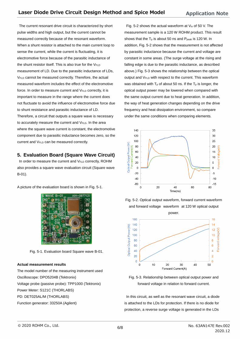
Fig. 5-2 shows the actual waveform at Vin of 50 V. The
measurement sample is a 120 W ROHM product. This result
shows that the Tp is about 50 ns and Ppeak is 120 W. In
addition, Fig. 5-2 shows that the measurement is not affected
by parasitic inductance because the current and voltage are
constant in some areas. (The surge voltage at the rising and
falling edge is due to the parasitic inductance, as described
above.) Fig. 5-3 shows the relationship between the optical
output and VFLD with respect to the current. This waveform
was obtained with Tp of about 50 ns. If the Tp is longer, the
optical output power may be lowered when compared with
the same output current due to heat generation. In addition,
the way of heat generation changes depending on the drive
frequency and heat dissipation environment, so compare
under the same conditions when comparing elements.
Fig. 5-2. Optical output waveform, forward current waveform
and forward voltage waveform at 120 W optical output
power.
Fig. 5-3. Relationship between optical output power and
forward voltage in relation to forward current.
In this circuit, as well as the resonant wave circuit, a diode
is attached to the LDs for protection. If there is no diode for
protection, a reverse surge voltage is generated in the LDs

7/8 © 2020 ROHM Co., Ltd. No. 63AN147E Rev.0022020.12
Laser Diode Drive Circuit Design Method and Spice Model Application Note
immediately after the circuit is turned off. Moreover, even
after the reverse surge voltage, the voltage of the DC
component continues to be applied to the LDs in the opposite
direction, which may destroy the element. Attaching a
protective diode makes it possible to control the reverse
surge voltage and stabilize the voltage to almost 0 V even
after the surge voltage is generated. For this reason, it is
important to connect protective diodes in order to prevent the
destruction of the LD elements, for details see Chapter 6,
which compares the case with and without protective diodes
using simulation.
6. Simulation Models and Demo Circuits ROHM also provides the Spice Model to simplify the
preliminary study.
Please refer to the following page for more information on
how to use it and download the model.
https://www.rohm.co.jp/products/laser-diodes/high-power-
lasers
ROHM's Spice model for LDs not only models the forward
current, forward voltage drops, capacitance characteristics
and leakage current characteristics, but also the optical
output. This makes it possible to design circuits in a simulator
and easily predict the optical output. (The optical output can
be checked by using the OPT terminal of the optical output
model. In this case, connect the GND terminal to GND. The
optical output power unit is in V [volts] but multiply the output
result by 1 A and convert it to W [watts].) However, this model
is modeled on the assumption that the optical output
waveform is the same as the forward current waveform, so if
you want to make a more accurate calculation, please
consider a different method.
Fig. 6-1 shows a comparison between the simulation results
and the actual measurement results for each characteristic of
ROHM's 120 W product. This result confirms that the
simulation results are almost identical to the actual
measurement results. The simulation results are shown in
Fig. 6-2, using a demo circuit for the Resonant wave B-01
evaluation board. By using this circuit, we can confirm not
only the optical output waveform but also the current that is
difficult to measure in the resonant circuit because of
inductance electromotive force.
Fig. 6-1. Comparison of measured and simulated results (a)
Forward voltage characteristics (b) Optical output
characteristics (c) Leakage current characteristics (d)
Capacitance characteristics.
Fig. 6-2. Demo circuit for Resonant wave B-01.
About the demonstration circuit corresponding to
Square wave B-01's circuit
Fig. 6-3 shows the simulation results of the voltage applied
to the LDs with and without the protective diode. When we
measure applied voltage of LD, the result includes the
inductance components of LD, the actual voltage applied to
the LD cannot be confirmed. In the simulation, the voltage
directly applied to the LD elements is confirmed.
With the protection diode, as shown in Fig. 6-3, the voltage
becomes close to zero immediately after switching. On the
other hand, without the protection diode, the voltage is
almost fixed at a negative voltage after switching. Under this
simulation conditions, a voltage of about -20 V is applied,
and the device is driven under conditions that continue to
exceed the reverse voltage withstand voltage of -4 V. As a
result, the possibility of element breakage will increase if a
protective diode is not installed, so the installation of a
protective diode is recommended.
Current
Optical output power

8/8 © 2020 ROHM Co., Ltd. No. 63AN147E Rev.0022020.12
Laser Diode Drive Circuit Design Method and Spice Model Application Note
Fig. 6-3. Confirmation of the effect of the protection diode by
Simulation.
7. References *1 G. A. Howe, "Capabilities and performance of dual-
wavelength Echidna® lidar," Journal of Applied Remote
Sensing 9(1), 095979, Dec 2015
*2 Efficient Power Conversion Corp., “Optimizing PCB
Layout,” 2019.
*3 J. Glaser, “High Power Nanosecond Pulse Laser Driver
Using an GaN FET,” PCIM Europe 2018 Proceedings, 2

R1102Bwww.rohm.com© 2016 ROHM Co., Ltd. All rights reserved.
Notice
ROHM Customer Support System https://www.rohm.com/contact/
Thank you for your accessing to ROHM product informations. More detail product informations and catalogs are available, please contact us.
N o t e s
The information contained herein is subject to change without notice.
Before you use our Products, please contact our sales representative and verify the latest specifica-tions :
Although ROHM is continuously working to improve product reliability and quality, semicon-ductors can break down and malfunction due to various factors.Therefore, in order to prevent personal injury or fire arising from failure, please take safety measures such as complying with the derating characteristics, implementing redundant and fire prevention designs, and utilizing backups and fail-safe procedures. ROHM shall have no responsibility for any damages arising out of the use of our Poducts beyond the rating specified by ROHM.
Examples of application circuits, circuit constants and any other information contained herein are provided only to illustrate the standard usage and operations of the Products. The peripheral conditions must be taken into account when designing circuits for mass production.
The technical information specified herein is intended only to show the typical functions of and examples of application circuits for the Products. ROHM does not grant you, explicitly or implicitly, any license to use or exercise intellectual property or other rights held by ROHM or any other parties. ROHM shall have no responsibility whatsoever for any dispute arising out of the use of such technical information.
The Products specified in this document are not designed to be radiation tolerant.
For use of our Products in applications requiring a high degree of reliability (as exemplified below), please contact and consult with a ROHM representative : transportation equipment (i.e. cars, ships, trains), primary communication equipment, traffic lights, fire/crime prevention, safety equipment, medical systems, servers, solar cells, and power transmission systems.
Do not use our Products in applications requiring extremely high reliability, such as aerospace equipment, nuclear power control systems, and submarine repeaters.
ROHM shall have no responsibility for any damages or injury arising from non-compliance with the recommended usage conditions and specifications contained herein.
ROHM has used reasonable care to ensure the accuracy of the information contained in this document. However, ROHM does not warrants that such information is error-free, and ROHM shall have no responsibility for any damages arising from any inaccuracy or misprint of such information.
Please use the Products in accordance with any applicable environmental laws and regulations, such as the RoHS Directive. For more details, including RoHS compatibility, please contact a ROHM sales office. ROHM shall have no responsibility for any damages or losses resulting non-compliance with any applicable laws or regulations.
When providing our Products and technologies contained in this document to other countries, you must abide by the procedures and provisions stipulated in all applicable export laws and regulations, including without limitation the US Export Administration Regulations and the Foreign Exchange and Foreign Trade Act.
This document, in part or in whole, may not be reprinted or reproduced without prior consent of ROHM.
1)
2)
3)
4)
5)
6)
7)
8)
9)
10)
11)
12)
13)
Recommended