Judul Artikel : The Effect of Temperature Variations on the Optical
Properties of Tin Oxide Film with Doping Aluminum,
Fluorin, and Indium for Semiconductor Electronic Devices
Penulis : Aris Doyan, Susilawati, dan Muhammad Taufik
Nama Jurnal/Prosiding : The 5th
International Conference on Functional Materials
Science (ICFMS 2020)
Volume Jurnal : 1028
Halaman : 77-83
ISSN : 1662-9752
Penerbit : Materials Science Forum (Scientific.Net)
DOI : https://doi.org/10.4028/www.scientific.net/MSF.1028.77
Alamat Web Jurnal : https://www.scientific.net/MSF.1028.77
URL Dokumen : https://www.scientific.net/MSF.1028.77.pdf
Tanggal/Waktu : April 2021
Satuan : 1 Makalah/Tahun
Volume Kegiatan : 1

Profil Jurnal


Artikel Tulisan Author yang Terbit di Materials Science
Forum (Scientific.Net)

The Effect of Temperature Variations on the Optical Properties of Tin Oxide Film with Doping Aluminum, Fluorine and Indium for
Semiconductor Electronic Devices
Aris Doyan1,2,a*, Susilawati1,2,b, and Muhammad Taufik1,c 1Physics Education, FKIP, University of Mataram, Lombok, West Nusa Tenggara, Indonesia
2Master of Science Education Program, University of Mataram, Lombok, West Nusa Tenggara, Indonesia
a*[email protected] (corresponding author), [email protected], [email protected]
Keywords: Tin optical properties, tin oxide film, doping aluminium, fluorine, indium.
Abstract. The manufacture of a thin layer of SnO2: (Al + F + In) was carried out by using the sol-
gel spin coating method on a glass substrate with various temperatures (25, 50, 100, 150, and
200 0C).The purpose of this study is to determine the optical properties of thin layers which include
transmittance, absorbance, band gap energy and activation energy. The optical properties of the
coating were characterized using a UV-Vis spectrophotometer with a wavelength of 200-1100 nm.
The results showed that the absorbance value increased with increasing temperature at a wavelength
of 300 nm. The absorbance values obtained for temperature variations were in the percentages of
95: 5% and 75: 25%, respectively 3.46-4.50 and 3.96-5.76. The transmittance value obtained
increased, namely 73.00-86.30% and 74.20-99.30%. In addition, the energy band gap decreased
from 3.60-3.41 eV and 3.57-3.31 eV for direct allowed, while 3.69-3.58 eV and 3.65-3.54 eV for
indirect allowed. Activation energy decreased from 2.00-1.18 eV and 1.60-1.12 eV. In general, the
absorbance and transmittance values increase with increasing ripening temperature and the addition
of doping aluminum, fluorine, and indium, while the bandgap energy and activation energy values
obtained decrease with increasing ripening temperature and increasing the doping percentage of
aluminum, fluorine, and indium. The decrease in the value of the bandgap energy and the activation
energy can make it easier for electrons to move from the valence band to the conduction band so
that the material is slightly conductive and acts as a semiconductor.
Introduction
The Semiconductors are materials that are flexible, meaning that in certain circumstances they
act as conductors and in other cases are insulators [1]. Various ways have been done by researchers
to maximize the function of semiconductor materials, including modifying the material in the form
of a thin layer.
The use of thin layers of semiconductor materials includes gas sensors, [2], LED (Light emited
diode) [3], solar cells [4], TCO (transparent Conducting Oxide) which are used in transparent
electrodes [5], LCD [6] and so forth. The types of materials that have been utilized in the synthesis
of thin films are titanium dioxide [7], aluminum, tungsten disulfide [8], and tin oxide [9].
The level of sensitivity of a thin film material is influenced by its optical properties. The optical
property referred to is the energy value of the thin layer band gap. The higher the bandgap energy
value of the layer, the more difficult the material is to conduct current. The bandgap energy value of
the tin oxide (SnO2) thin layer is still quite high, around 3.72 eV [10], so it needs to be modified by
adding donors or other atoms to the material. Several other atoms are added namely, ferrum [11],
aluminum-zinc [12], indium [13] and fluorine [14]. In this study, the doping materials used are
aluminum, fluorine, and indium with the hope that the layer transparency rate increases and the
bandgap energy obtained is lower than the previous band gap energy.
Materials Science Forum Submitted: 2020-11-10ISSN: 1662-9752, Vol. 1028, pp 77-83 Revised: 2020-12-09doi:10.4028/www.scientific.net/MSF.1028.77 Accepted: 2020-12-19© 2021 Trans Tech Publications Ltd, Switzerland Online: 2021-04-29
All rights reserved. No part of contents of this paper may be reproduced or transmitted in any form or by any means without the written permission of TransTech Publications Ltd, www.scientific.net. (#561322423-10/06/21,06:20:26)

Experiments
The stages of this research consisted of synthesis and characterization. The first stage, synthesis,
is the process of making a thin layer using the sol-gel spin coating technique with a SnO2: (Al + F +
In) ratio of 95: 5% and 75: 25%. The synthesis consists of glass substrate preparation, sol-gel
preparation, coating preparation, and curing [15]. Substrate preparation is done by cleaning the
glass with detergent to remove all the dirt on the glass. Sol-gel making is done by dissolving SnO2,
aluminum, fluorine, and indium in ethanol (C2H5OH) using a magnetic stirrer until a thick white
solution is formed, then left for 24 hours. The coating was made using a spin coater with a rotating
time of 3 minutes. The thin layer that has been formed is then heated with temperature variations of
25, 50, 100, 150, and 200 0C using a furnace for 1 hour. The second stage, namely characterization
of thin films using the UV-Vis Spectrophotometer Thermo Scientific Genesys 150 with a
wavelength of 200-1100 nm.
Result and Discussion
The results obtained from the synthesis of a thin layer of SnO2 with doping aluminum, fluorine
and indium (SnO2: Al + F + In) made the layer formed more transparent. This is shown in Figures 1
and 2, where a thin layer of SnO2: (Al + F + In) with a doping concentration of 75: 25% (Figure 2)
is more transparent than a thin layer of SnO2: (Al+F +In) with a doping concentration of 95: 5%
(Figure 1).
(a) (b) (c) (d) (e)
Figure 1. SnO2 thin layer: (Al +F + In) (95: 5%) temperature variations (a) 25 0C,
(b) 50 0C, (3) 100 0C, (d) 150 0C, (e) 200 0C.
(a) (b) (c) (d) (e)
Figure 2. SnO2 thin layer: (Al + F + In) (75: 25%) temperature variations (a) 25 0C,
(b) 50 0C, (3) 100 0C, (d) 150 0C, (e) 200 0C.
The next analysis is characterization of the optical properties of thin films using UV-Vis. The
data obtained from the results of characterization of optical properties include absorbance,
transmittance, band gap energy and activation energy.
Absorbance
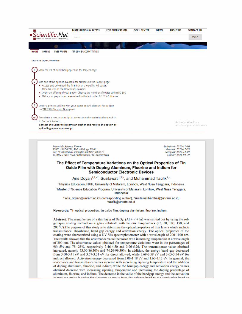
Figure 3 shows the relationship between the wavelength and the absorbance of the SnO2: (Al + F
+ In) thin film temperature variations.
78 Functional Materials: Fundamental Research and Industrial Application
(a) (b)
Figure 3. Graph of wavelength relationship with absorbance of thin layer SnO2: (Al + F + In)
temperature variation. (a) 95: 5%, (b) 75: 25%.
In Figure 3, it is clear that the absorbance value of the SnO2: (Al +F + In) thin film absorbs
temperature variations. The maximum absorbance values for temperature variations of 25, 50, 100,
150 and 200 0C for the percentages 95: 5% and 75: 25% at a wavelength of 300 nm are 3.46-4.50
and (Figure 3a) and 3.96-5.76 (Figure 3b), respectively. Based on Figure 3, it is clear that the higher
the temperature, the resulting absorbance value increases, especially in the ultraviolet region with a
wavelength of 300 nm.
Transmittance
The graph of the relationship between the wavelength and the transmittance of the SnO2: (Al + F
+ In) thin layer variation is shown in the following figure.
(a) (b)
Figure 4. The graph of the wavelength relationship with the transmittance of the thin layer SnO2:
(Al + F + In) temperature variation (a) 95: 5%, (b) 75: 25%.
The transmittance value for temperature variations in the 300-800 nm wave range is shown in
Figure 4.The transmittance values for temperature variations of 25, 50, 100, 150 and 200 0C are 95:
5% and 75: 25% respectively 73.00-86.30% ( Figure 4a) and 74.20-99.30% (Figure 4b). This means
that the transmittance value increases with increasing temperature. This is because the energy
possessed by photons is smaller than the energy gap so that it is unable to excite electrons. This
resulted in the photons being only transmitted [16].
0
1
2
3
4
5
200 250 300 350 400
Ab
sorb
ance
Wavelength (nm)
25°C
50°C
100°C
150°C
200°C
0
1
2
3
4
5
6
200 250 300 350 400
Ab
sorb
ance
Wavelength (nm)
25°C
50°C
100°C
150°C
200°C
0
10
20
30
40
50
60
70
80
90
300 400 500 600 700 800
Tran
smit
ance
(%
)
Wavelength (nm)
25°C
50°C
100°C
150°C
200°C
0
20
40
60
80
100
300 400 500 600 700 800
Tran
smit
ance
(%
)
Wavelength (nm)
25°C
50°C
100°C
150°C
200°C
Materials Science Forum Vol. 1028 79

Bandgap Energy
Bandgap energy consists of direct allowed bandgap energy and indirect allowed bandgap energy.
Bandgap energy is obtained by graphing the photon energy with respect to (αhυ)r. The amount of
bandgap energy is shown by the slope of the photon energy graph with respect to (αhυ)r. The
amount of bandgap energy is obtained from equation 1 [17]. While the activation energy of the thin
layer is obtained from 1/m or one per gradient of the photon energy graph with respect to ln 𝛼 .
𝛼(ℎ𝜐)ℎ𝜐 = 𝐾(ℎ𝜐 − 𝐸𝑔)𝑟 (1)
Note: α is the absorbance coefficient, hυ is the incident energy of the photon, K is a constant, r =
1/2 for direct and r = 2 for indirect band-gap energy. Based on equation 1, it is obtained that the
direct and indirect energy band gap allowed for the SnO2: (Al + F + In) layer with the tauc plot
method is shown in Figures 5 and 6.
(a) (b)
Figure 5. Energy band gap direct allowed SnO2: (Al + F + In) thin layer. (a) 95: 5%, (b) 75: 25%.
(a) (b)
Figure 6. Energy band gap indirect allowed SnO2: (Al + F + In) thin layer. (a) 95: 5%, (b) 75: 25%.
0
500
1000
1500
2000
3.4 3.5 3.6 3.7 3.8 3.9 4 4.1 4.2 4.3 4.4
(αhƲ)1
/2 (e
V/m
)1/2
E (eV)
25°C
50°C
100°C
150°C
200°C
0
100
200
300
400
500
3.3 3.4 3.5 3.6 3.7 3.8 3.9 4 4.1 4.2 4.3 4.4
(αhƲ)1
/2 (e
V/m
)1/2
E (eV)
25°C50°C100°C150°C200°C
0
5E+15
1E+16
1.5E+16
2E+16
3.5 3.6 3.7 3.8 3.9 4 4.1 4.2 4.3 4.4
(αhƲ)2
(eV
/m)2
E (eV)
25°C
50°C
100°C
150°C
200°C
0
1E+15
2E+15
3E+15
4E+15
5E+15
6E+15
3.5 3.6 3.7 3.8 3.9 4 4.1 4.2
(αhƲ)2
(eV
/m)2
E (eV)
25°C50°C100°C150°C200°C
80 Functional Materials: Fundamental Research and Industrial Application

(a) (b)
Figure 7. The relationship between temperature variations and the energy band gap of the SnO2:
(Al + F + In) thin layer. (a) 95: 5%, (b) 75: 25%.
Figure 7 shows that the band gap energy values for temperature variations. The band gap energy
values for temperature variations of 25, 50, 100, 150 and 200 0C for a percentage of 95: 5% (Figure
7a) are 3.60, 3.53, 3.50, 3.43 and 3.41 eV for direct allowed, respectively, while for indirect
allowed respectively 3.69, 3.66, 3.64, 3.61, and 3.58 eV, respectively. The energy value of the band
gap for temperature variation for the percentage of 75: 25% (Figure 7b) is 3.57, 3.54, 3.48, 3.43,
and 3.31 eV for direct allowed, respectively, while for indirect allowed the amount is 3.65, 3.62,
3.60, 3.57, respectively and 3.54 eV. The energy band gap obtained decreases with increasing
ripening temperature and increasing the doping percentage of aluminum, fluorine, and indium [18,
19].
Activation Energy
Activation energy can be obtained from the slope of the straight line ln (α) versus photon energy
(hυ). The value of ln (α) is obtained from the equation.
𝛼(υ) = 𝛼0 exp (𝐸𝑓
𝐸𝑢) (2)
Where α (υ) = absorption coefficient, α0= constant, Ef = photon energy, and Eu = Urbach energy.
The values for Ln (α) and the activation energy are shown in Figures 8 and 9.
(a) (b)
Figure 8. Graph of the relationship between photon energy and ln (α) of the SnO2: (Al + F + In)
layer variation. (a) 95: 5%, (b) 75: 25%.
y = 0.001T + C, R² = 0.9374
y = 0.0006T + C, R² = 0.9838
3.3
3.4
3.5
3.6
3.7
3.8
0 50 100 150 200
Eg (
eV
)
Temperature (C)
Direct
Indirect
y = 0.0014T + C, R² = 0.9673
y = 0.0006T + C, R² = 0.98383.2
3.3
3.4
3.5
3.6
3.7
0 50 100 150 200
Eg (
eV
)
Temperature (C)
Direct
Indirect
0
5
10
15
20
25
30
35
3.3 3.4 3.5 3.6 3.7 3.8 3.9 4
Ln (α)
E (eV)
Ln Alfa 200°C Ln Alfa 150°C
Ln Alfa 100°C Ln Alfa 50°C
Ln Alfa 25°C
0
10
20
30
40
3.3 3.4 3.5 3.6 3.7 3.8 3.9 4
Ln (α)
E (eV)
Ln Alfa 200°C Ln Alfa 150°C
Ln Alfa 100°C Ln Alfa 50°C
Ln Alfa 25°C
Materials Science Forum Vol. 1028 81

(a) (b)
Figure 9. The relationship between temperature variations and the activation energy of the SnO2:
(Al + F + In) thin film. (a) 95: 5%, (b) 75: 25%.
Figure 9 shows that the activation energy for temperature variations of 25, 50, 100, 150 and 200 0C for a percentage of 95: 5% (Figure 9a) is 2.00, 1.84, 1.76, 1.72 and 1.18 eV, respectively, while
for a percentage of 75: 25% 1.60, 1.47, 1.41, 1.37, 1.12 eV, respectively. In general, the activation
energy decreases with increasing ripening temperature and the doping percentage of aluminum,
fluorine, and indium. This shows that the movement of electrons increases so that the transfer of
electrons from the valence band to the conduction band increases [20, 21].
Summary
The synthesis of SnO2: (Al + F + In) thin films has been carried out using the sol-gel spin
coating technique. The data obtained from the characteristics of the optical properties include
absorbance, transmittance, band gap energy and activation energy. In the ultraviolet area with a
wavelength of 300 nm, the absorbance value increases with the increase in ripening temperature and
the addition of doping of aluminum, fluorine, and indium, while the transmittance value increases at
a wavelength of 350 nm to 800 nm in the area (ultraviolet-visible) as the ripening temperature
increases. and increasing amounts of aluminum, fluorine, and indium doping. In general, the
absorbance and transmittance values increase with increasing ripening temperature and the addition
of doping aluminum, fluorine, and indium, while the bandgap energy and activation energy values
obtained decrease with increasing ripening temperature and increasing the doping percentage of
aluminum, fluorine, and indium. This is because the energy possessed by photons is smaller than
the energy gap so that it is unable to excite electrons and results in the photons being only
transmitted. In addition, the bandgap energy and activation energy obtained decreased with
increasing ripening temperature and increasing the doping percentage of aluminum, fluorine, and
indium. The decrease in the value of the bandgap energy and the activation energy can make it
easier for electrons to move from the valence band to the conduction band so that the material is
slightly conductive and acts as a semiconductor.
Acknowledgment
A big thank you to the students the material physics research groups have tried to help prepare
samples and data retrieval. Thank you very much to the education department of research and
technology for the fundamental grant research in years 2018 until 2020. Thank you to Diponegoro
University Integrated Laboratory, all staff and laboratory analytical chemistry Mataram University
and Laboratory Nano Technology ITB.
y = 0.004T + C, R² = 0.8241
0
0.5
1
1.5
2
2.5
0 50 100 150 200
Ea (
eV
)
Temperature (C)
y = 0.0023T + C, R² = 0.8974
0
0.5
1
1.5
2
0 50 100 150 200
Ea (
eV
)
Temperature (C)
82 Functional Materials: Fundamental Research and Industrial Application
References
[1] A. Mandelis, Physics Today, 72(10), 68-69 (2019).
[2] C. L. Lu, S. J. Chang, T. C. Weng, and T. J. Hsueh, IEEE Electron Device Letters, 39 (8),
1223 – 1225 ( 2018).
[3] B. Kashyout, Fathy, Gad, Badr, and A. Bishara, Photonics, 6(2) (2019).
[4] F. Bittau, A. Abbas, K. L. Barth, J.W. Bowers, and J. M. Walls, Thin Solid Films, (633), 92-
96 (2017).
[5] B. Sarma, D. Barman, and B. K. Sarma, Applied Surface Science, (479), 786-795 (2019).
[6] D. F. Andrade, F.M. Fortunato, and E. R. Pereira-Filho, Analytica Chimica Acta,(1061), 42-49
(2019).
[7] M.R. Panigrahi, and M. Devi, Journal of Physics: Conference Series, 1172, 012046 (2019).
[8] A. S. Pawbake, R. G. Waykar, D.J. Late, and S.R. Jadkar, ACS Applied Materials &
Interfaces, 8(5), 3359–3365 (2016).
[9] M. A Yıldırım, S. T. Yıldırım, , E. F. Sakar, and A. Ates, Spectrochimica Acta Part A:
Molecular and Biomolecular Spectroscopy, 133, 60–65 (2014).
[10] D.L. Kamble, N.S. Harale, V.L. Patil, P.S. Patil, and L.D. Kadam, Journal of Analytical and
Applied Pyrolysis, 127, 38–46 (2017).
[11] B. Beklesovas, V. Stankus, J. Link, R. Stern, Thin Solid Films, (708), 138-124 (2020).
[12] A. Doyan, Susilawati, N. Ikraman, and M. Taufik, Journal of Physics: Conference Series,
1011, 1-6 (2018).
[13] S. Hakim, A. Doyan, Susilawati, L. Muliyadi, Journal of Research in Science Education, 5 (2),
171-174 (2019).
[14] L. Muliyadi, A. Doyan, Susilawati, and S. Hakim, Journal of Research in Science Education,
5(2), 175-178 (2019).
[15] Susilawati, A. Doyan, L. Muliyadi, and S. Hakim, Journal of Research in Science Education,
6 (1), 1-4 (2019).
[16] Susilawati, A. Doyan, L. Muliyadi, S. Hakim, M. Taufik, and Nazarudin. Journal of Physics:
Conference Series, 1397, 1-8 (2019).
[17] Susilawati, and A. Doyan, American Journal of Applied Science, 6 (12), 2071-2077 (2009).
[18] A. Doyan, Susilawati, A. Harjono, S. Azzahra, and M. Taufik, Materials Science Forum, 966,
30-34 (2019).
[19] M. S. Bannur, A. Antony, K. I. Maddani, P. Poornesh, A. Rao, and K.S. Choudhari, Physica E:
Low-Dimensional Systems and Nanostructures, 103, 348–353 (2018).
[20] G. Bhatia, V. K. Gupta, M. M. Patidar, S.B. Srivasatava, D. Singh, M. Gangrade, and V.
Ganesan, AIP Conference Proceedings 1953, 100084 (2018).
[21] A. Doyan, Susilawati, S. Hakim, L. Muliyadi, M. Taufik, Journal of Physics: Conference
Series, 1397, 1-8 (2019).
Materials Science Forum Vol. 1028 83

Corresponding Author dengan Pihak 5th
ICFMS 2020
Certificate of Participation
This is to certify that
Aris Doyan
has participated as
Oral Presenter
in the 5th International Conference on Functional Materials Science 2020
(the 5th ICFMS 2020) held online on November 11-12, 2020
Organized by:
UI, UNPAD, ITB, ITS, and UGM
Chairman of the 5th ICFMS 2020
Budhy Kurniawan


Recommended


![]SEDIA TEKNIK · 2020. 5. 13. · Setiap tulisan yang dimuat dalam jurnal media teknik ini akan dinilai terlebih da hulu oleh pakar ... judul lengkap artikel (bila bukan buku), judul](https://img.pdfslide.us/doc/110x75/6132f32cdfd10f4dd73ac68a/sedia-teknik-2020-5-13-setiap-tulisan-yang-dimuat-dalam-jurnal-media-teknik.jpg)