244 • 2010 IEEE International Solid-State Circuits Conference
ISSCC 2010 / SESSION 13 / FREQUENCY & CLOCK SYNTHESIS / 13.1
13.1 A Low-Area Switched-Resistor Loop-Filter Technique for Fractional-N Synthesizers Applied to a MEMS-Based Programmable Oscillator
Michael H Perrott1, Sudhakar Pamarti2, Eric Hoffman3, Fred S Lee1,Shouvik Mukherjee1, Cathy Lee1, Vadim Tsinker4, Sathi Perumal5,Benjamin Soto6, Niveditha Arumugam1, Bruno W Garlepp1
1SiTime, Sunnyvale, CA 2University of California, Los Angeles, CA 3Global Foundries, Sunnyvale, CA 4Invensense, Sunnyvale, CA 5Consultant, Sunnyvale, CA 6Consultant, Mountain View, CA
MEMS resonators have recently emerged as an alternative structure to crystalresonators in providing frequency references which achieve better than 50 ppmaccuracy over the industrial temperature range. As illustrated in Fig. 13.1.1, aprogrammable oscillator utilizing a MEMS resonator is achieved by wire bond-ing a MEMS resonator die to a CMOS die that contains an oscillator sustainingcircuit, temperature sensor, fractional-N synthesizer, and various digital blocks.The output of the sustaining circuit provides a 5 MHz reference frequency to thefractional-N synthesizer, which outputs a higher frequency that can be digitallyadjusted with sub-ppm resolution over a >10% tuning range. By then sendingthe fractional-N synthesizer output into a programmable frequency divider (i.e.,divide-by-N circuit), any frequency in the range of 1 to 115 MHz can be achievedby proper combination of the fractional-N synthesizer and programmable dividersettings.
As shown in Fig. 13.1.1, the sub-ppm tuning capability of the fractional-N syn-thesizer enables straightforward compensation of frequency deviation in theMEMS resonator due to temperature variation. In particular, a temperature sen-sor on the CMOS die is utilized in combination with digital logic that performspolynomial multiplication of the digitized temperature value in order to compen-sate for curvature in the MEMS frequency variation across temperature. TheMEMS resonator utilized in this work has sufficient part-to-part consistency inits temperature to frequency characteristic such that better than 50 ppm accura-cy can be achieved from -40 to 85 degrees C.
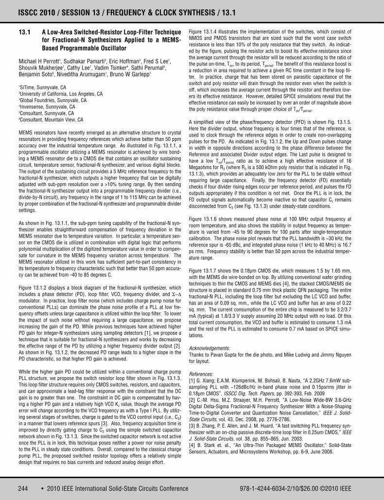
Figure 13.1.2 displays a block diagram of the fractional-N synthesizer, whichincludes a phase detector (PD), loop filter, VCO, frequency divider, and Σ−Δmodulator. In practice, loop filter noise (which includes charge pump noise forconventional PLLs) can dominate the phase noise profile of a PLL at low fre-quency offsets unless large capacitance is utilized within the loop filter. To lowerthe impact of such noise without requiring a large capacitance, we proposeincreasing the gain of the PD. While previous techniques have achieved higherPD gain for integer-N synthesizers using sampling detectors [1], we propose atechnique that is suitable for fractional-N synthesizers and works by decreasingthe effective range of the PD by utilizing a higher frequency divider output [2].As shown in Fig. 13.1.2, the decreased PD range leads to a higher slope in thePD characteristic, so that higher PD gain is achieved.
While the higher gain PD could be utilized within a conventional charge pumpPLL structure, we propose the switch resistor loop filter shown in Fig. 13.1.3.This loop filter structure requires only CMOS switches, resistors, and capacitors,and can approximate a lead-lag filter response with the constraint that the DCgain is no greater than one. The constraint in DC gain is compensated by hav-ing a higher PD gain and a relatively high VCO Kv value, though the average PDerror will change according to the VCO frequency as with a Type I PLL. By utiliz-ing several stages of switches, charge is gated to the VCO control input (i.e., C3)in a manner that lowers reference spurs [3]. Also, frequency acquisition time isimproved by directly gating charge to C3 using the simple switched capacitornetwork shown in Fig. 13.1.3. Since the switched capacitor network is not activeonce the PLL is in lock, this technique poses neither a power nor noise penaltyto the PLL in steady state conditions. Overall, compared to the classical chargepump PLL, the proposed switched resistor topology offers a relatively simpledesign that requires no bias currents and reduced analog design effort.
Figure 13.1.4 illustrates the implementation of the switches, which consist ofNMOS and PMOS transistors that are sized such that the worst case switchresistance is less than 10% of the poly resistance that they switch. As indicat-ed by the figure, pulsing the resistor acts to boost its effective resistance sincethe average current through the resistor will be reduced according to the ratio ofthe pulse on-time, Ton, to its period, Tperiod. The benefit of this resistance boost isa reduction in area required to achieve a given RC time constant in the loop fil-ter. In practice, charge that has been stored on parasitic capacitance of theswitch and poly resistor will drain through the resistor even when the switch isoff, which increases the average current through the resistor and therefore low-ers its effective resistance. However, detailed SPICE simulations reveal that theeffective resistance can easily be increased by over an order of magnitude abovethe poly resistance value through proper choice of Ton/Tperiod.
A simplified view of the phase/frequency detector (PFD) is shown Fig. 13.1.5.Here the divider output, whose frequency is four times that of the reference, isused to clock through the reference edges in order to create non-overlappingpulses for the PD. As indicated in Fig. 13.1.2, the Up and Down pulses changein width in opposite directions according to the phase difference between theReference and associated Divider output edges. The Last pulse is designed tohave a low Ton/Tperiod ratio as to achieve a high effective resistance of 16Megaohms for R3 (where R3 is a 500 kOhm poly resistor that is indicated in Fig.13.1.3), which provides an adequately low zero for the PLL to be stable withoutrequiring large capacitance. Finally, the frequency detector (FD) essentiallychecks if four divider rising edges occur per reference period, and pulses the FDoutputs appropriately if this condition is not met. Once the PLL is in lock, theFD output signals automatically become inactive so that capacitor Cc remainsdisconnected from C3 (see Fig. 13.1.3) under steady-state conditions.
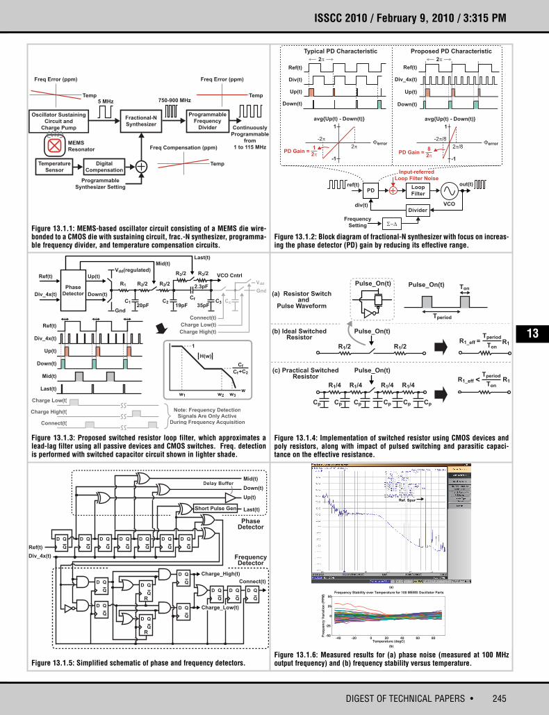
Figure 13.1.6 shows measured phase noise at 100 MHz output frequency atroom temperature, and also shows the stability in output frequency as temper-ature is varied from -45 to 90 degrees for 100 parts after single-temperature calibration. The phase noise plot reveals that the PLL bandwidth is ~30 kHz, thereference spur is -65 dBc, and integrated phase noise (1 kHz to 40 MHz) is 16.7ps rms. Frequency stability is better than 50 ppm across the industrial temper-ature range.
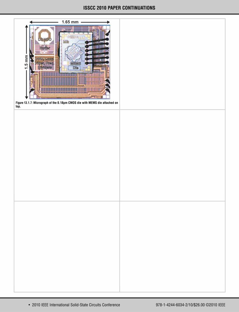
Figure 13.1.7 shows the 0.18µm CMOS die, which measures 1.5 by 1.65 mm,with the MEMS die wire-bonded on top. By utilizing conventional wafer grindingtechniques to thin the CMOS and MEMS dies [4], the stacked CMOS/MEMS diestructure is placed in standard 0.75 mm thick plastic QFN packaging. The entirefractional-N PLL, including the loop filter but excluding the LC VCO and buffer,has an area of 0.09 sq. mm., while the LC VCO and buffer has an area of 0.22sq. mm. The current consumption of the entire chip is measured to be 3.2/3.7mA (typical) at 1.8/3.3 V supply assuming 20 MHz output with no load. Of thistotal current consumption, the VCO and buffer is estimated to consume 1.3 mAand the rest of the PLL is estimated to consume 0.7 mA based on SPICE simu-lations.
Acknowledgements:Thanks to Pavan Gupta for the die photo, and Mike Ludwig and Jimmy Nguyenfor layout.
References:[1] G. Xiang; E.A.M. Klumperink, M. Bohsali, B. Nauta, “A 2.2GHz 7.6mW sub-sampling PLL with −126dBc/Hz in-band phase noise and 0.15psrms jitter in0.18µm CMOS”, ISSCC Dig. Tech. Papers, pp. 392-393, Feb. 2009[2] C.-M. Hsu, M.Z. Straayer, M.H. Perrott, “A Low-Noise Wide-BW 3.6-GHzDigital Delta-Sigma Fractional-N Frequency Synthesizer With a Noise-ShapingTime-to-Digital Converter and Quantization Noise Cancellation,” IEEE J. Solid-State Circuits, vol. 43, Dec. 2008, pp. 2776-2786.[3] B. Zhang, P. E. Allen, and J. M. Huard, “A fast switching PLL frequency syn-thesizer with an on-chip passive discrete-time loop filter in 0.25um CMOS,” IEEEJ. Solid-State Circuits, vol. 38, pp. 855–865, Jun. 2003.[4] B. Stark et. al., “An Ultra-Thin Packaged MEMS Oscillator,” Solid-StateSensors, Actuators, and Microsystems Workshop, pp. 6-9, June 2008.
978-1-4244-6034-2/10/$26.00 ©2010 IEEE
245DIGEST OF TECHNICAL PAPERS •
ISSCC 2010 / February 9, 2010 / 3:315 PM
Figure 13.1.1: MEMS-based oscillator circuit consisting of a MEMS die wire-bonded to a CMOS die with sustaining circuit, frac.-N synthesizer, programma-ble frequency divider, and temperature compensation circuits.
Figure 13.1.2: Block diagram of fractional-N synthesizer with focus on increas-ing the phase detector (PD) gain by reducing its effective range.
Figure 13.1.3: Proposed switched resistor loop filter, which approximates alead-lag filter using all passive devices and CMOS switches. Freq. detectionis performed with switched capacitor circuit shown in lighter shade.
Figure 13.1.5: Simplified schematic of phase and frequency detectors.Figure 13.1.6: Measured results for (a) phase noise (measured at 100 MHzoutput frequency) and (b) frequency stability versus temperature.
Figure 13.1.4: Implementation of switched resistor using CMOS devices andpoly resistors, along with impact of pulsed switching and parasitic capaci-tance on the effective resistance.
Fractional-N
Synthesizer
Oscillator Sustaining
Circuit and
Charge Pump
Temp
Freq Error (ppm)
Digital
Compensation
Temperature
SensorTemp
Freq Compensation (ppm)
Temp
Freq Error (ppm)
Continuously
Programmable
from
1 to 115 MHzMEMS
Resonator
5 MHz
Programmable
Synthesizer Setting
750-900 MHz
Programmable
Frequency
Divider
out(t)ref(t)
VCODivider
div(t)
Loop
FilterPD
2πΦerror
avg{Up(t) - Down(t)}
-2π
1
-1
PD Gain = 2π
1
2π
Div(t)
Ref(t)
Up(t)
Down(t)
Div_4x(t)
Ref(t)
Up(t)
Down(t)
2π
2π/8Φerror
avg{Up(t) - Down(t)}
-2π/8
1
-1
PD Gain = 2π
8
Σ−Δ
Frequency
Setting
Typical PD Characteristic Proposed PD Characteristic
Input-referred
Loop Filter Noise
Vdd(regulated)
Gnd
Phase
Detector
Ref(t)
Div_4x(t)
Up(t)
Down(t)
R1 R2/2 R2/2
R3/2 R3/2
C1 C2 C3Cf
Mid(t)Last(t)
Ref(t)
Div_4x(t)
Up(t)
Down(t)
Mid(t)
Last(t)
VCO Cntrl
w
Cf+C2
Cf
1
w1 w2 w3
H(w)
Cc
Vdd
Gnd
Charge Low(t)
Charge High(t)
Connect(t)
Charge Low(t)
Charge High(t)
Connect(t)
Note: Frequency DetectionSignals Are Only Active
During Frequency Acquisition
35pF19pF20pF
2.3pF
Pulse_On(t)
Pulse_On(t) Ton
Tperiod
Pulse_On(t)
R1/2
CpCp Cp CpCpCp
R1/2
R1/4R1/4 R1/4 R1/4
Ton
TperiodR1
Ton
TperiodR1<
R1_eff =
R1_eff
(b) Ideal SwitchedResistor
(c) Practical SwitchedResistor
(a) Resistor Switch and
Pulse Waveform
Pulse_On(t)
Ref(t)
Div_4x(t)
D Q
Q
D Q
Q
D Q
Q
D Q
Q
D Q
Q
D Q
Q
D Q
Q
D Q
Q
D Q
Q
D Q
Q
D Q
Q
D Q
QR
D Q
QR
D Q
Q
D Q
Q
D Q
Q
Connect(t)
Charge_High(t)
Charge_Low(t)
Up(t)
Down(t)
Mid(t)Delay Buffer
Last(t)
PhaseDetector
FrequencyDetector
Short Pulse Gen
Ref. Spur
-40 -20 0 20 40 60 80-50
-25
0
25
50
Temperature (degC)
Fre
qu
ency
Var
iati
on
(P
PM
) Frequency Stability over Temperature for 100 MEMS Oscillator Parts
(a)
(b)
13
• 2010 IEEE International Solid-State Circuits Conference 978-1-4244-6034-2/10/$26.00 ©2010 IEEE
ISSCC 2010 PAPER CONTINUATIONS
Figure 13.1.7: Micrograph of the 0.18µm CMOS die with MEMS die attached ontop.
LC VCOLC VCO
&
BufferBuffer
PFD, LoopPFD, Loop
Filter, Freq.Filter, Freq.
DividersDividers
1.65 mm1
.5 m
m
MEMSMEMS
DieDie
Recommended