Internal Hardware Design of a Microcontroller in VLSI
Designers:Shreya Prasad
andHeather Smith
Advisor:Dr. Vinod Prasad
Date:May 12th, 2003

Abstract
This project describes the design and implementation of some of the internal hardware
components of a microcontroller. The subsystems designed are the fundamental
hardware components necessary to create the 16-bit timer’s input capture and output
compare modes, the index register, and other systems. The subsystems designed were the
clock controller, the 16-bit timer, the register controller, the register, and the comparator.
The project engineers implemented their system using Xilinx to test their logic and VLSI
to construct the gates. VHDL code was written in order to implement the project onto an
FPGA board.

Table of Contents
Introduction 4
System Description 4
Block Diagrams 5
Clock Controller Subsystem 5
16-bit Timer Subsystem 5
Register Controller Subsystem 6
Register Subsystem 7
Comparator Subsystem 7
Analysis of Results 8
Gate-Level Design in Xilinx 8
VLSI Circuit Diagrams in L-Edit 13
Computer Simulations of VLSI Design in PSpice 18
VHDL Software Design 23
Conclusions 24
Appendix: VHDL Subsystem Code and Simulation 25

Introduction
The purpose of the Capstone project is to design some of the internal components
of a microcontroller. The subsystems designed are the fundamental hardware
components necessary to create the 16-bit timer’s input capture and output compare
modes, the index register, and other systems. The delays created by the system can run
real-time systems and interrupts. These delays are important in creating PWM signals
and also in the operation of the microcontroller.
System Description
The designers used a top-down approach. Figure 1 shows the complete system
block diagram. The system has five main subsystems: the clock controller, the timer, the
register controller, the register, and the comparator. The user inputs are the clock pulse,
the 8-bit value into the accumulator, the 1-bit enable and the 2-bit control value to the
register controller, the 1-bit enable and the 2-bit control value to the clock controller, the
enable to the 16-bit timer, and various resets for each subsystem. The user outputs are a
1-bit value from each of the four comparators and a 1-bit overflow from the timer.
Figure 1: System Block Diagram

Block Diagrams
Clock Controller Subsystem
The clock controller accepts from the user a clock pulse input and an enable input
to turn on the counter, as shown in Figure 2. The user’s clock pulse is used as the clock
pulse input to each of the three D flip-flops in the counter. The outputs of the three D
flip-flops are four clock pulses, which are one time, two times, four times, and eight
times the period of the original pulse. The user also will input a 2-bit control value to
select which of the four pulses will be used as the system clock by a 4:1 multiplexor.
Figure 2: Clock Controller Subsystem Block Diagram
16-bit Timer Subsystem
As can be seen in Figure 3, the inputs to the timer subsystem are the enable and
the reset from the user and the clock from the clock controller. The outputs are the lower
8 bits of the 16-bit timer value, which input to the comparator subsystem, and the
overflow bit, which is an external carry out bit. The timer operates as a 16-bit counter.
After FFFFh has been reached, it sets the carry out bit high for one clock pulse and
restarts at 0000h.

Figure 3: 16-bit Timer Subsystem Block Diagram
Register Controller Subsystem
The user will input a 2-bit value that tells the controller which of the four registers
should store the accumulator value. The clock input to the subsystem comes from the
clock controller. Figure 4 shows how the register controller’s four outputs are connected
to the clocks of each of the four registers. The register controller selects which register
will receive the accumulator value by turning that register’s clock on and leaving all of
the other registers’ clock inputs low. If the enable input to the controller is low, none of
the registers will receive the accumulator value.
Figure 4: Register Controller and Register Subsystems Block Diagram
Register Subsystem
The 8-bit accumulator is where the user enters the value to be stored. The
accumulator consists of eight D flip-flops, each holding a single bit. The accumulator, as
shown in Figure 4, can then transfer the value into any of the four registers depending on
which register’s clock is turned on by the register controller.
The register subsystem is closely related to the register controller as just
described. Figure 4 shows the four 8-bit registers, which receive the clock pulse from the
register controller. The inputs to the register subsystem are the 8-bit accumulator value,
the clock from the register controller, and a reset for each register. Each of the four
registers contains eight D flip-flops, making a total of thirty-two D flip-flops for the
register subsystem. The subsystem stores 8-bit values received from the accumulator
until the user enters a new value into the register specified by the register controller. In
this case, the new value would simply replace the previous value. The subsystem also
outputs each of the 8-bit values to the comparator.
Comparator Subsystem
The comparator subsystem has two inputs: an 8-bit value from each of the
registers in the register subsystem and the lower 8-bit value from the timer subsystem.
The output of each comparator is a one-bit compare value, as shown in Figure 5. There
are four comparators, one for each of the four registers. In this subsystem, the 8-bit value
from each register is compared to the lower 8-bits from the timer. If the two eight bit
values are the same, the 1-bit output is logic ‘1.’ Otherwise, the output is logic ‘0.’

Figure 5: Comparator Subsystem Block Diagram
Analysis of Results
The gate-level schematics of the subsystems were designed and simulated using
Xilinx Foundation 4. L-Edit Pro was used to create the transistor-level design using
VLSI. The extract file generated from each L-Edit design was edited and tested in
PSpice. VHDL code was written and tested for each subsystem using ModelSim. The
system was made into one project in Xilinx, L-Edit, and ModelSim. The designers
implemented the complete VHDL project onto an FPGA board using Xilinx Foundation.
Gate-Level Design in Xilinx
The design began at the gate-level where the digital logic could be easily tested
and debugged before moving onto a VLSI design in L-Edit, which is a more complex
working environment. Each subsystem was designed separately in a schematic file and
simulated. Once each subsystem was proved to be working, the subsystems were then
turned into macros, which was done by creating a single block entity from a schematic
file. These blocks show only the inputs and outputs of each schematic and simplify the
layout when connecting the subsystems together, as shown in Figure 10.

The clock controller in Figure 6 has a 3-bit counter on the left half and a 4:1
multiplexor on the right half. The user inputs a clock pulse and the subsystem outputs the
clock pulse selected by the 2-bit user control value on the bottom of Figure 6.
Figure 6: Gate-Level Design of Clock Controller Subsystem
Figure 7 shows a 4-bit counter design. The timer subsystem consists of four of
these to make the 16-bit timer. The final AND gate on the bottom outputs the carry out
bit. The design will have 16 falling-edge D flip-flops and a reset.
Figure 7: Gate-Level Design of 4-bit Timer
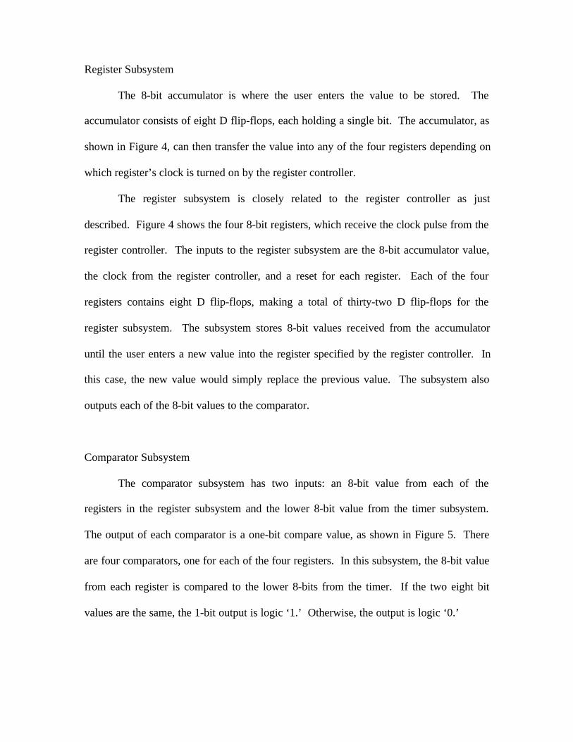
The register controller subsystem accepts a 2-bit controller value, which selects
which of the four output bits will take the input clock pulse. This is done by using a 2:4
decoder, as shown in Figure 7.
Figure 7: Gate-Level Design of the Register Controller
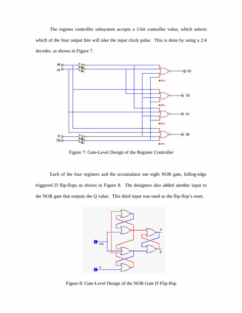
Each of the four registers and the accumulator use eight NOR gate, falling-edge
triggered D flip-flops as shown in Figure 8. The designers also added another input to
the NOR gate that outputs the Q value. This third input was used as the flip-flop’s reset.
Figure 8: Gate-Level Design of the NOR Gate D Flip-flop

As shown in Figure 9, the comparator design used XOR gates to compare the
register and timer values bit by bit. A NAND gate was used to verify if all eight of the
bits were the same.
Figure 9: Gate-Level Design of the Comparator Subsystem
Complete System
The complete system is shown in Figure 10. The designers used macros to create
blocks for various subsystems.

Figure 10: System Gate-Level Design in Xilinx

VLSI Circuit Diagrams in L-Edit
The VLSI system design was accomplished using the software package L-Edit.
All of the subsystems in VLSI are based on the gate-level designs shown in Figures 6
through 10. The D flip-flop, shown in Figure 11, uses six NOR gates. This design uses
the least number of transistors, which is important because the D flip-flop is integral in
three of the subsystems: the clock controller, the 16-bit timer, and the register.
Figure 11: D Flip-Flop Design in VLSI
The clock controller subsystem is shown in Figure 12. The 3-bit counter is on the
left side and the 4:1 multiplexor is on the right.

Figure 12: Clock Controller Subsystem in VLSI
Figure 13 shows the 16-bit timer subsystem design in VLSI. Each of the four
columns represents four bits of the counter with the most significant bits on the left hand
side.

Figure 13: 16-bit Timer Subsystem in VLSI
An 8-bit register is made up of 8 D flip-flops. As shown in Figure 14, there are
four flip-flops on the top row and four on the bottom. In a single register all the flip-flops
have their clocks and resets tied together. The four registers and the accumulator use this
design.
Figure 14: 8-bit Register Design in VLSI

The comparator subsystem in L-Edit is shown in Figure 15. The eight two-input
XOR gates are shown to the left, and their outputs go into the eight-input NOR gate
shown to the right.
Figure 15: Comparator Subsystem in VLSI

The VLSI design for the complete subsystem is shown in Figure 16.
Figure 16: Complete System Design in VLSI

Computer Simulations of VLSI Design in PSpice
PSpice was used to simulate the L-Edit designs. The PSpice simulation for each
subsystem is shown below. The system simulation is also shown.
Clock Controller Subsystem:
The input clock pulse is the bottom plot in Figure 17. This subsystem outputs one
of four clock pulses to the system depending on the 2-bit controller input value, which are
the two middle plots. The working output plot is displayed on the top line.
Figure 17: Clock Controller Output Plot in PSpice
Timer Subsystem:
The 16-bit timer subsystem works as a 16-bit counter. Figure 18 shows it
working as a 4-bit counter since it would be excessive to display all sixteen output bits.
The input clock is the bottom plot. Here the carry out bit from the eleventh bit is set high
to enable the last four bits to act as if the first four bits. Testing was done in a similar
manner by simulating the system in four 4-bit increments. This was the final test,

showing the most significant four bits of the timer and the carry out bit, which is the top
most plot in Figure 18.
Figure 18: 16-bit Timer Output Plot in PSpice
Register Controller Subsystem:
The simulation shown in Figure 19 shows how one of the four outputs, shown as
the top four plots, takes the input clock pulse depending on the 2-bit controller value. If
the enable is low, none of the four outputs will take the clock pulse, as shown during the
first half of the simulation.
Figure 19: Register Controller Plot in PSpice

Register Subsystem:
The register subsystem consists of four 8-bit registers. Each bit is a single D flip-
flop, which is shown in Figure 20. Reset, the bottom plot, must be low for the output, the
top plot, to take the input, which is the second to top plot. The output only follows the
input on the falling edge of the clock, which is the second to bottom plot.
In the subsystem, the resets and clocks of all the D flip-flops of the same register
area tied together.
Figure 20: D Flip-Flop Used by the Register Subsystem in PSpice
Comparator Subsystem:
In Figure 21, the output at the top goes high when all four of the input plots
shown are the same. The bottom two inputs would come from the timer and the middle
two input plots would come from a register. The system compares two sets of eight bits,
but for simplicity, the designers used the same to describe multiple input variables.

Figure 21: Comparator Subsystem in PSpice
Complete System:
To test the complete system, the designers first needed to initialize all of the
subsystems by setting reset high. Once this was done, the timer, as shown in Figure 20,
started incrementing from 0000h.
Figure 22: Timer Output of Complete System in PSpice
Next, values were entered into the accumulator and the register controller
assigned these values to the appropriate register.

Figure 23: Register 2 Outputs and Compare 2 Output
The designers also stored values into register 3 and plotted the output of
comparator 3 to test if the system is working. This is shown in Figure 24, which can be
compared to the timer values in Figure 24. The outputs of comparator 0 and 1 were also
checked but since the registers’ values remained at all zero, the compare output only went
high when the timer first started at all zeros.
Figure 24: Register 3 Outputs and Compare 3 Output

VHDL Software Design
The VHDL code for each of the five subsystems is shown in the appendix.
Components were created in individual files. The components were combined using the
gate level design from Xilinx. Port maps were used to call each component and define
the inputs and outputs. The code for the entire system is shown in Figure 25. The
simulation is shown in Figure 26.
library ieee;use ieee.std_logic_1164.all;entity system isport( t: in std_logic_vector(15 downto 0);
Q1,Q2,Q3,Q4: in std_logic_vector(7 downto 0);Out1,Out2,Out3,Out4: out std_logic);
end system;
architecture sgp of system iscomponent clkcontimport (etimer,eclkcon,restimer,resclkcon,clkin: in std_logic;
conclk: in std_logic_vector (1 downto 0);t: out std_logic_vector (15 downto 0);co: out std_logic);
end component;component regport (Da: in std_logic_vector(7 downto 0);
a: in std_logic_vector(1 downto 0);clk,rst,enable: in std_logic;Q1,Q2,Q3,Q4:out std_logic_vector(7 downto 0));
end component;component compport (r:in std_logic_vector(7 downto 0); t:in std_logic_vector(15 downto 0);
z:out std_logic);end component;begin
g15: comp port map(Q1,t,Out1);g16: comp port map(Q2,t,Out2);g17: comp port map(Q3,t,Out3);g18: comp port map(Q4,t,Out4);
end sgp;Figure 24: VHDL code for System
Figure 25: Simulation of System code

Conclusion
The Capstone Project was successful. The designers successfully created the
internal components in Xilinx, L-EDIT, and VHDL that they had set out to do. They
were able to implement their VHDL design onto an FPGA board successfully and
demonstrate it at the Technology Expo. The designers now have a better understanding
of the internals of a microcontroller.

Appendix: VHDL Subsystem Code and Simulation
The five subsystems are shown with their simulation output.
Comparator subsystem:
library ieee;use ieee.std_logic_1164.all;
entity comp isport(r,t:in std_logic_vector(7 downto 0); z:out std_logic);end comp;
architecture sgp of comp iscomponent xor_gate isport(x,y: in std_logic; z: out std_logic);end component;
component nor8_gateport(input: in std_logic_vector(7 downto 0); output:out std_logic);
end component;
signal s: std_logic_vector(7 downto 0);begin
g1:xor_gate port map(r(0),t(0),s(0));g2:xor_gate port map(r(1),t(1),s(1));g3:xor_gate port map(r(2),t(2),s(2));g4:xor_gate port map(r(3),t(3),s(3));g5:xor_gate port map(r(4),t(4),s(4));g6:xor_gate port map(r(5),t(5),s(5));g7:xor_gate port map(r(6),t(6),s(6));g8:xor_gate port map(r(7),t(7),s(7));g9:nor8_gate port map(s,z);
end sgp;Figure A1: VHDL code for Comparator subsystem
Figure A2: Simulation for Comparator

Figure A3: Simulation for Comparator (zoomed in)
Register Subsystem and Register Controller Subsystem:
library ieee;use ieee.std_logic_1164.all;
entity reg isport(Da: in std_logic_vector(7 downto 0);
a: in std_logic_vector(1 downto 0);clk,rst,enable: in std_logic;Q1,Q2,Q3,Q4:out std_logic_vector(7 downto 0));
end reg;
architecture sgp of reg iscomponent reg8
port(D:in std_logic_vector(7 downto 0);clk,rst: in std_logic;Q: out std_logic_vector(7 downto 0));
end component;
component regconport(a: in std_logic_vector (1 downto 0);enable,clk: in std_logic;clock_out: out std_logic_vector (3 downto 0));
end component;
component accport(Da: in std_logic_vector(7 downto 0);clk,rst:in std_logic;Qa:out std_logic_vector(7 downto 0));
end component;
signal clock_out: std_logic_vector(3 downto 0);signal Qa: std_logic_vector(7 downto 0);
beging9:reg8 port map(D=>Qa,clk=>clock_out(0),rst => rst,Q=>Q1);g10:reg8 port map(D=>Qa,clk=>clock_out(1),rst => rst,Q=>Q2);g11:reg8 port map(D=>Qa,clk=>clock_out(2),rst => rst,Q=>Q3);g12:reg8 port map(D=>Qa,clk=>clock_out(3),rst => rst,Q=>Q4);g13:acc port map(Da=>Da,clk=>clk,rst=>rst, Qa=>Qa);g14:regcon port map(a=>a, clk=>clk, enable=>enable,
clock_out=>clock_out);
end sgp;Figure A4: VHDL code for Register subsystem

Figure A5: Simulation for Register
Clock Controller Subsystem:
library ieee;use ieee.std_logic_1164.all;
entity clkcon isport (eclkcon,clkin,resclkcon: in std_logic;conclk: in std_logic_vector (1 downto 0);d,q: inout std_logic_vector (2 downto 0);clk: out std_logic);
end clkcon;
architecture rtl of clkcon iscomponent and2
port (x,y: in std_logic;z: out std_logic);
end component;
component xor_gateport (x,y: in std_logic;z: out std_logic);
end component;
component dffport(D,clk,rst: in std_logic;Q: out std_logic);
end component;
component not1port(x: in std_logic;z: out std_logic);
end component;
component nand3port (w,x,y: in std_logic;z: out std_logic);
end component;
component nand4port (v,w,x,y: in std_logic;z: out std_logic);
end component;
signal e,f: std_logic;signal na0,na1: std_logic;signal g,h,i,j: std_logic;

beging1: xor_gate port map (eclkcon,q(0),d(0));g2: and2 port map (eclkcon,q(0),e);g3: dff port map (d(0),clkin,resclkcon,q(0));
g4: xor_gate port map (e,q(1),d(1));g5: and2 port map (e,q(1),f);g6: dff port map (d(1),clkin,resclkcon,q(1));
g7: xor_gate port map (f,q(2),d(2));g9: dff port map (d(2),clkin,resclkcon,q(2));
g10: not1 port map (conclk(0),na0);g11: not1 port map (conclk(1),na1);g12: nand3 port map (clkin,na1,na0,g);g13: nand3 port map (q(0),na1,conclk(0),h);g14: nand3 port map (q(1),conclk(1),na0,i);g15: nand3 port map (q(2),conclk(1),conclk(0),j);g16: nand4 port map (g,h,i,j,clk);
end rtl;
Figure A6: VHDL code for Clock Controller
Figure A7: Simulation for Clock Controller
Timer:library ieee;use ieee.std_logic_1164.all;
entity timer isport (etimer,clk,restimer: in std_logic;co: out std_logic;t: out std_logic_vector (15 downto 0));
end timer;
architecture rtl of timer iscomponent and2
port (x,y: in std_logic;z: out std_logic);
end component;
component xor_gateport (x,y: in std_logic;z: out std_logic);
end component;
component dffport(D,clk,rst: in std_logic;Q: out std_logic);
end component;
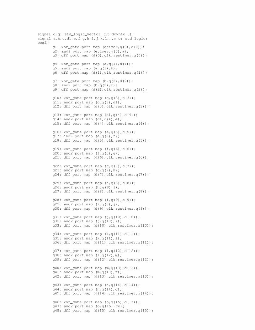
signal d,q: std_logic_vector (15 downto 0);signal a,b,c,d1,e,f,g,h,i,j,k,l,n,m,o: std_logic;begin
g1: xor_gate port map (etimer,q(0),d(0));g2: and2 port map (etimer,q(0),a);g3: dff port map (d(0),clk,restimer,q(0));
g4: xor_gate port map (a,q(1),d(1));g5: and2 port map (a,q(1),b);g6: dff port map (d(1),clk,restimer,q(1));
g7: xor_gate port map (b,q(2),d(2));g8: and2 port map (b,q(2),c);g9: dff port map (d(2),clk,restimer,q(2));
g10: xor_gate port map (c,q(3),d(3));g11: and2 port map (c,q(3),d1);g12: dff port map (d(3),clk,restimer,q(3));
g13: xor_gate port map (d1,q(4),d(4));g14: and2 port map (d1,q(4),e);g15: dff port map (d(4),clk,restimer,q(4));
g16: xor_gate port map (e,q(5),d(5));g17: and2 port map (e,q(5),f);g18: dff port map (d(5),clk,restimer,q(5));
g19: xor_gate port map (f,q(6),d(6));g20: and2 port map (f,q(6),g);g21: dff port map (d(6),clk,restimer,q(6));
g22: xor_gate port map (g,q(7),d(7));g23: and2 port map (g,q(7),h);g24: dff port map (d(7),clk,restimer,q(7));
g25: xor_gate port map (h,q(8),d(8));g26: and2 port map (h,q(8),i);g27: dff port map (d(8),clk,restimer,q(8));
g28: xor_gate port map (i,q(9),d(9));g29: and2 port map (i,q(9),j);g30: dff port map (d(9),clk,restimer,q(9));
g31: xor_gate port map (j,q(10),d(10));g32: and2 port map (j,q(10),k);g33: dff port map (d(10),clk,restimer,q(10));
g34: xor_gate port map (k,q(11),d(11));g35: and2 port map (k,q(11),l);g36: dff port map (d(11),clk,restimer,q(11));
g37: xor_gate port map (l,q(12),d(12));g38: and2 port map (l,q(12),m);g39: dff port map (d(12),clk,restimer,q(12));
g40: xor_gate port map (m,q(13),d(13));g41: and2 port map (m,q(13),n);g42: dff port map (d(13),clk,restimer,q(13));
g43: xor_gate port map (n,q(14),d(14));g44: and2 port map (n,q(14),o);g45: dff port map (d(14),clk,restimer,q(14));
g46: xor_gate port map (o,q(15),d(15));g47: and2 port map (o,q(15),co);g48: dff port map (d(15),clk,restimer,q(15));

process (q)beginfor i in 0 to 15 loopt(i) <= q(i);end loop;end process;
end rtl;
Figure A8: VHDL code for Timer Subsystem
Figure A9: Simulation for Timer
Recommended