
INTEGRATED OPTICAL FILTERS BASED ON
MICRORING RESONATORS
Freddy Tan
The research described in this thesis was carried out at the Integrated Optical
MicroSystems (IOMS) Group, Faculty of Electrical Engineering, Mathematics
and Computer Science, MESA+ Research Institute, University of Twente,
P.O.Box 217, 7500 AE Enschede, The Netherlands.
This work was supported financially by the BTS project ringresonatoren
(Senter) for the first two years and the last two years by the European
Commission (EC) funded Information Society Technologies (IST) project Next-
generation Active Integrated optic Subsystems (NAIS), with contract number
IST-2000-28018.
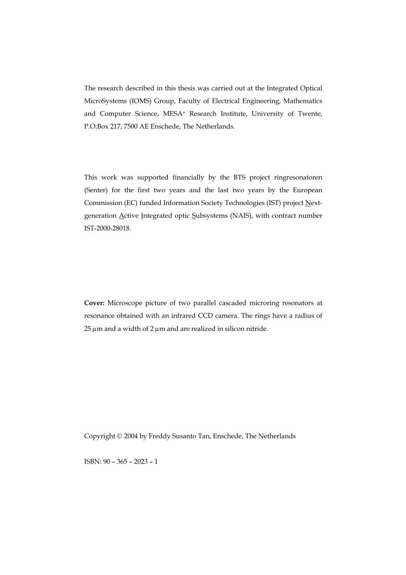
Cover: Microscope picture of two parallel cascaded microring resonators at
resonance obtained with an infrared CCD camera. The rings have a radius of
25 µm and a width of 2 µm and are realized in silicon nitride.
Copyright © 2004 by Freddy Susanto Tan, Enschede, The Netherlands ISBN: 90 – 365 – 2023 – 1
INTEGRATED OPTICAL FILTERS BASED ON
MICRORING RESONATORS
PROEFSCHRIFT
ter verkrijging van
de graad van doctor aan de Universiteit Twente,
op gezag van de rector magnificus,
prof. dr. F.A. van Vught,
volgens besluit van het College voor Promoties
in het openbaar te verdedigen
op vrijdag 20 februari 2004 om 13.15 uur
door
Freddy Susanto Tan
geboren op 24 november 1966
te Bandung, Indonesië

Dit proefschrift is goedgekeurd door:
De promotor Prof. Dr. A. Driessen

This thesis is dedicated to My father and the memory of my mother My wife and children

Contents Chapter 1. Introduction 1
1.1 Optical communication 1
1.2 Optical filters in WDM systems 3
1.3 BTS project ringresonatoren 5
1.4 IST project Next-generation Active Integrated optics
Subsystem (NAIS) project 6
1.5 Outline of the thesis 8
Chapter 2. General concepts of microring resonator devices 11
2.1 Microring resonator devices 11
2.2 Working principle of microring resonator devices 12
2.3 The lateral and vertical coupling configuration 15
2.3.1 The lateral coupling configuration 15
2.3.2 The vertical coupling configuration 16
2.4 Cascaded multiple microring resonator devices 17
2.4.1 Serial configuration 17
2.4.2 Parallel configuration 18
2.5 Performance of microring resonator devices 20
2.6 Characterization methods 23
Conclusions 25
Chapter 3. Design strategy 27
3.1 Input fields for the design activity 27
3.1.1 Knowledge 27
3.1.2 Previous experiences 29
3.1.3 Design tools 30
3.1.4 Technology and facilities 32
3.1.5 Objectives 33
3.1.6 Time frame 34
3.1.7 System specifications 34
3.2 Field of specific activities 35
3.2.1 Design 35
3.2.2 Realization 37
3.2.3 Intermediate characterization 37
3.2.4 Functional characterization 38
3.2.5 System demonstrator 39
Conclusions 39
Chapter 4. High finesse single-ring resonator devices based on a lateral
coupling configuration for WDM applications 41
Chapter 5. Single microring resonator devices based on a vertical
coupling configuration 47
5.1 Silicon Oxynitride based microring resonator devices 47
5.1.1 Design considerations 48
5.1.2 Fabrication process for the complete devices 49
5.1.3 Device performance 53
5.2 Characterization of vertically waveguide coupled microring
resonators by means of quantitative image analysis 56
5.3 Silicon Nitride based microring resonator devices 64
5.3.1 Design considerations 64
5.3.2 Fabrication process for the complete devices 65
5.3.3 Device performance 66
5.3.4 High finesse vertically coupled waveguide-microring
resonators based on Si3N4-SiO2 technology 67
Conclusions 70
Chapter 6. Cascaded multiple microring resonators as optical bandpass
filter 71
6.1 Design of cascaded multiple microring resonators in
the parallel configuration 72
6.2 Fabrication process of cascaded multiple microring
resonators in the parallel configuration 73
6.3 Simulation model of cascaded multiple microring resonators
in the parallel configuration 75
6.4 Experimental results 76
Conclusions 80
Chapter 7. Compact spectral slicer devices based on microring
resonators 81
7.1 Introduction 81
7.2 Design of compact spectral slicers based on vertically coupled
microring resonators 81
7.3 Realization of the spectral slicer devices 87
7.4 Experimental results 87
Conclusions 90
Chapter 8. Summary and Recommendations 93
8.1 Summary 93
8.2 Recommendations 95
References 99
Publications 109
Acknowledgment 115
Curriculum Vitae 117

Chapter 1 _______________________________________________________________________________________
1
Chapter 1
Introduction
1.1 Optical communication The invention of the laser in 1960 [Maiman 1960] made available a coherent
(i.e. monochromatic) radiation source some 104 – 105 times higher in frequency
than the existing microwave generators with a frequency of about 1010 Hz.
Since then much efforts has been spent to use the laser for communications. It
was thought that a communication systems operating at optical frequencies
would increase the information carrying capacity by as much as 100,000 times
compared to the microwave systems existing at that time. Besides the light
source also transmission lines were needed with low transmission loss to
arrive eventually at optical communication systems.
In 1966, glass optical fibers had been considered as suitable and effective
transmission lines but their losses were still high. In 1970, Kapron, et al.
[Kapron 1970] from Corning Glass Works fabricated a silica fiber with an
attenuation of 20 dB/km. At this attenuation level, the repeater spacing for
optical fiber links becomes comparable to those of copper systems making the
lightwave technology a practical alternative. In the next two decades, data
transmission via optical fiber became more and more attractive because the
attenuation of the optical fibers could be reduced below 0.2 dB/km in the 1550
nm wavelength window.
The devices that are employed in present day communication systems are a
combination of electronic and optical technology. In long distance
communication links, mostly optical fibers have been used and sophisticated
devices have been developed with extremely high performance with respect to
transmission speed, the number of wavelengths and the transmission distance.
Introduction _______________________________________________________________________________________
2
As many users share the costs of these devices, bulk optics technology can be
used with extremely good technical performance but very high cost. In short
distance links, where only a few users can share the costs, mostly electronic
devices are in use nevertheless their limited transmission capacity.
Nowadays, metropolitan networks are already optical and access networks
are becoming more and more optical. The adaptation of solutions from long
distance communications are probably not appropriate anymore for access
network where the single users are responsible for the cost by themselves. For
the implementation in access network, one needs optical systems and devices,
which operating at high bit rates (> Gbit/s) allow complex optical routing and
data processing and are compact and low-cost without need of maintenance
by trained engineers [Driessen 2003].
The rapid growth in demand for high-capacity telecommunication links and
the speed limitation of electronics used in single-wavelength optical links have
resulted in an extraordinary increase in the use of wavelength division
multiplexing (WDM). A WDM system can multiply the transmission capacity
of a single optical fiber link several times by multiplexing a large number of
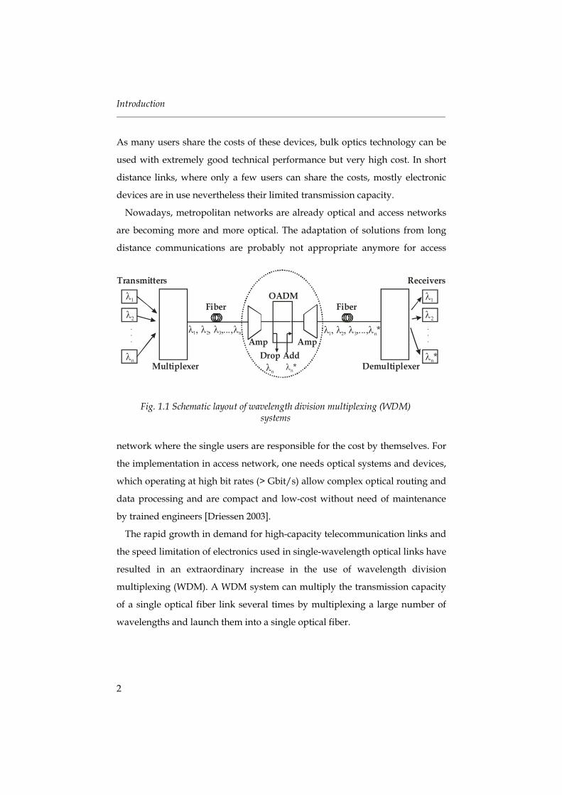
wavelengths and launch them into a single optical fiber.
Fig. 1.1 Schematic layout of wavelength division multiplexing (WDM) systems
Transmitters
Dropλn
Addλn*
λ , λ , λ ,...,λ1 2 3 n λ , λ , λ ,...,1 2 3 λn*
OADM
Amp Amp
Fiber Fiberλ1
Multiplexer Demultiplexer
Receivers
.
.
.
λ2
λn
λ1
.
.
.
λ2
λn*
Chapter 1 _______________________________________________________________________________________
3
Basic components in a point to point WDM connection are transmitters,
multiplexer, optical fiber link with perhaps optical amplifiers, demultiplexers
and receivers. For additional nodes in between, optical add-drop multiplexers
(OADM) are necessary. This situation is schematically depicted in Fig. 1.1. At
the transmitter side a WDM multiplexer connects the optical signals from N
transmitters operating each at its own wavelength, λn to a single optical fiber.
At the OADM, a signal of one or more specific wavelengths is dropped and
new data on the same wavelengths are added. The signals arriving at the
demultiplexer will be demultiplexed and each wavelength will be directed to
one of the N receivers.
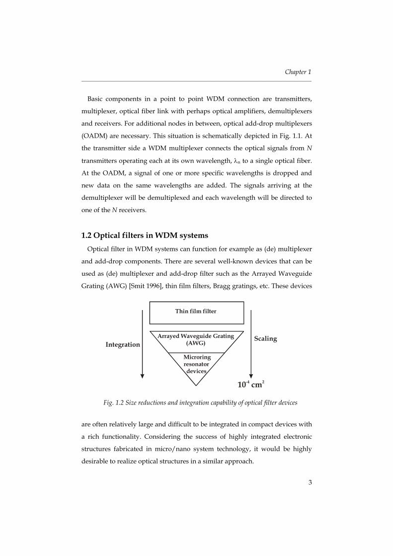
1.2 Optical filters in WDM systems Optical filter in WDM systems can function for example as (de) multiplexer
and add-drop components. There are several well-known devices that can be
used as (de) multiplexer and add-drop filter such as the Arrayed Waveguide
Grating (AWG) [Smit 1996], thin film filters, Bragg gratings, etc. These devices
are often relatively large and difficult to be integrated in compact devices with
a rich functionality. Considering the success of highly integrated electronic
structures fabricated in micro/nano system technology, it would be highly
desirable to realize optical structures in a similar approach.
Fig. 1.2 Size reductions and integration capability of optical filter devices
Integration
Thin film filter
Arrayed Waveguide Grating (AWG)
Microring resonatordevices
Scaling
10 cm-4 2
Introduction _______________________________________________________________________________________
4
Integrated optical filters based on microring resonators can become as small as
10-4 cm2 and could be promising functional elements in future large scale
integrated photonics, see Fig.1.2. Compact optical filter devices based on
microring resonators have been proposed since 1997 [Little 1997]. A cascaded
six microring resonator device in a serial configuration (see also Sec. 2.4) has
been announced on October 9, 2003 by Little Optics, Inc. [Little 2003].
There are three classes of microring resonator devices, which can be used in
WDM applications. The first type is the microring resonator device with a Free
Spectral Range (FSR) equal to the distance between WDM channels of about 10
- 100 GHz (0.08 nm - 0.8 nm). The second type is a filter with a FSR covering a
large part of the WDM window that usually is related to the wavelength range
of 1530 - 1560 nm where erbium doped fiber amplifiers (EDFA) are available.
The third type is a microring based filter devices with a FSR larger than the
standard WDM window, typically 50 nm – 100 nm.
The microring devices in the first category can be realized by using a
moderate refractive index contrast material (∆n ~ 0.05) such as low index
contrast SiON/SiO2. They usually have a large radius of more than 300 µm to
be able to fit the FSR to the WDM channels. In this technology, conventional
optical photolithography can be applied for fabrication. Fiber to chip coupling
is usually not a problem because the straight waveguides have mode profiles
that usually fit to the standard optical fiber. Relatively low refractive index
contrast materials also mean lower scattering loss. Filters with a FSR of 50
GHz – 100 GHz and interleaver filter for 25 GHz spaced dense wavelength
division multiplexing systems based on a serial cascaded microring resonator
device (see also Sec. 2.4) have been realized by using this technology [Melloni
2003]. The second type of the microring devices can be fabricated by using a
large refractive index contrast material (∆n ~ 0.5) such as high refractive index
SiON or Si3N4 in combination with SiO2. A typical bending radius is 10 µm –
30 µm, corresponding to a FSR of about 8 nm - 20 nm.
Chapter 1 _______________________________________________________________________________________
5
Also this technology allows conventional optical photolithography in the
realization process. Therefore, the route to low-cost technology is feasible.
Fiber to chip coupling becomes critical in this technology, but simple tapering
sections and the use of small core fibers result in acceptable losses of a few
tenth of dB.
The microring devices belonging to the third category can only be realized
by using high refractive index contrast material (∆n > 2) such as Si/SiO2 or III-
V semiconductors and allow very small bend structure down to 2 µm – 5 µm.
For these devices, conventional mask-based photolithography can not be used
anymore. Only advanced deep UV techniques from the semiconductor
industry or direct e-beam writing can be used to obtain acceptable
performance. The propagation loss of these devices is relatively high (> 7
dB/cm) and mainly dominated by scattering loss due to the high refractive
index contrast in the materials [Dumon 2003]. Fiber to chip coupling loss is
usually very critical and becomes a problem in this technology.
This thesis presents devices consisting of single and parallel cascaded
multiple microring resonators (see also Sec. 2.4), which belong to the second
category that can be used as bandpass filters, spectral slicers and (de-)
multiplexers. The results that are presented in this thesis have been obtained
during the work within the framework of the BTS project “ringresonatoren”
and the IST project “Next-generation Active Integrated optics Subsystem
(NAIS)”.
1.3 BTS project ringresonatoren The aim of the BTS project “ringresonatoren” was the realization of
microring resonator devices, which can be used as an add-drop component in
future DWDM telecommunication networks. There were 3 partners involved
in this project founded by the Dutch Ministry of Economic Affairs: JDS
Uniphase, BBV software BV, and the Integrated Optical MicroSystems (IOMS)
Group (formerly Lightwave Devices Group).
Introduction _______________________________________________________________________________________
6
In the first phase the studies have been based on a lateral coupling
configuration. The material used for fabricating these devices was Low-
Pressure Chemical Vapor Deposition (LPCVD) Silicon Nitride (Si3N4) with a
refractive index of 1.98. This value was obtained by ellipsometric
measurements and was extrapolated for a wavelength of 1550 nm. The devices
have been designed to work for TE polarization to give sufficiently low
bending loss.
Later on, the design of the microring resonator device has been based on the
vertical coupling configuration. The LPCVD Si3N4 that has been used
previously can not be used anymore for the microring core due to the
requirement of polarization independence of the filter response. For the
fabrication of these resonator devices, which can support only the
fundamental TE and TM modes in vertical and radial directions Plasma
Enhanced Chemical Vapor Deposition Silicon Oxynitride (PECVD SiON) with
a refractive index of 1.65 has been chosen. It will be shown that it is difficult to
obtain a polarization independent response with single microring resonator
devices. By using a polarization diversity scheme, however, it is possible to
make a wavelength selective polarization independent splitter, as has been
proposed by Klunder et al. [Klunder 2002 (a)].
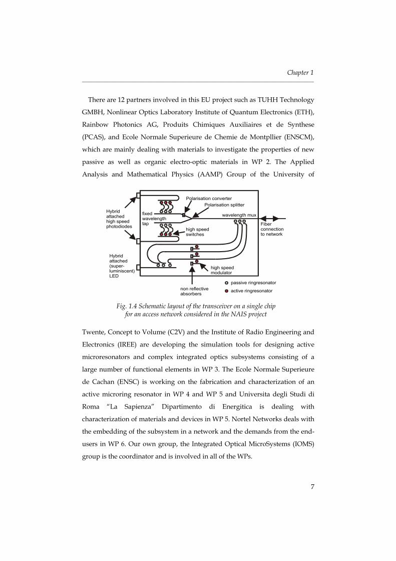
1.4 IST project Next-generation Active Integrated optics
Subsystem (NAIS) project The second project I have been involved in is the EC founded NAIS project,
which has the objective to demonstrate the feasibility of a next generation
compact integrated optics subsystem based on microring resonators as
depicted in Fig. 1.4 [NAIS project]. In order to reach this objective, five
technical Work Packages (WP’s) have been considered in the project plan:
materials research (WP 2), design activities (WP 3), technological realization
(WP 4), characterization (WP 5) and system aspects (WP 6).
Chapter 1 _______________________________________________________________________________________
7
There are 12 partners involved in this EU project such as TUHH Technology
GMBH, Nonlinear Optics Laboratory Institute of Quantum Electronics (ETH),
Rainbow Photonics AG, Produits Chimiques Auxiliaires et de Synthese
(PCAS), and Ecole Normale Superieure de Chemie de Montpllier (ENSCM),
which are mainly dealing with materials to investigate the properties of new
passive as well as organic electro-optic materials in WP 2. The Applied
Analysis and Mathematical Physics (AAMP) Group of the University of
Twente, Concept to Volume (C2V) and the Institute of Radio Engineering and
Electronics (IREE) are developing the simulation tools for designing active
microresonators and complex integrated optics subsystems consisting of a
large number of functional elements in WP 3. The Ecole Normale Superieure
de Cachan (ENSC) is working on the fabrication and characterization of an
active microring resonator in WP 4 and WP 5 and Universita degli Studi di
Roma “La Sapienza” Dipartimento di Energitica is dealing with
characterization of materials and devices in WP 5. Nortel Networks deals with
the embedding of the subsystem in a network and the demands from the end-
users in WP 6. Our own group, the Integrated Optical MicroSystems (IOMS)
group is the coordinator and is involved in all of the WPs.
Polarisation converterPolarisation splitter
Hybridattachedhigh speed photodiodes
Hybrid attached(super-luminiscent)LED
Fiberconnectionto network
non reflectiveabsorbers
passive ringresonator
active ringresonator
high speedmodulator
high speedswitches
fixedwavelengthtap
wavelength mux
Fig. 1.4 Schematic layout of the transceiver on a single chip for an access network considered in the NAIS project
Introduction _______________________________________________________________________________________
8
Within the NAIS project, the devices have been realized in the vertical
coupling configuration. Single microring resonator devices made of LPCVD
Si3N4 have been realized and demonstrated. Their drop response show narrow
passbands, relatively low ON-OFF ratio (rejection ratio) and narrow stopbands
due to the Lorentzian shape of the filter response obtained from the drop port.
In order to improve the filter performance, parallel cascaded two- and three-
ring resonator devices have been designed and realized in LPCVD Si3N4
technology. The wavelength response of these devices has shown a promising
functionality as a bandpass filter as well as spectral slicer device.
1.5 Outline of the thesis In the first phase of the present work, another Ph.D student, Dr. D.J.W
Klunder was also dealing with microring resonator devices. In his work,
devices with a lateral coupling configuration have been used [Klunder 2002
(b)]. The device information and basic theory already provided in that thesis is
not repeated in this thesis.
This thesis deals with the design, fabrication and characterization of passive
microring resonators devices. Chapter 1 gives an introduction to the
development in optical communications. In addition, the projects where I had
been involved are briefly presented. Chapter 2 introduces general concepts
and relevant basic theory of optical microresonators and can be used as
reference for the following chapters. Chapter 3 presents the design strategy for
the realization of demonstrator devices. Chapter 4 presents the result of single
microring resonator devices based on the lateral coupling configuration using
LPCVD Si3N4 for the microring resonator core. A through response with a
finesse of more than 100 has been demonstrated. Results on vertically coupled
single microring resonators with a SiON (BTS) or Si3N4 (NAIS) core are
discussed in Chapter 5. Chapter 6 presents the results of higher order filters.
Parallel cascaded two- and three- microring resonator devices with equal
coupling coefficient have been realized and demonstrated.

Chapter 1 _______________________________________________________________________________________
9
Chapter 7 discusses the feasibility of parallel cascaded microring resonators as
compact spectral slicers with increased spectral efficiency. Chapter 8 gives a
summary of this thesis and recommendations for future work.

Introduction _______________________________________________________________________________________
10
Chapter 2 _______________________________________________________________________________________
11
Chapter 2
General concepts of microring resonator devices
In this chapter, general concepts and the relevant basic theory of microring
resonators are presented. This includes also a discussion of the two possible
coupling schemes i.e. the lateral and vertical coupling configuration. After a
description of single resonator devices an analysis is given of the performance
of multi-microring structures.
2.1 Microring resonator devices The simplest configuration of a microring resonator device consists of one
straight waveguide and one ring resonator. This device can be used as an all-
pass filter [Madsen 1999] for applications as phase equalizer, dispersion
compensator or optical delay line [Madsen 1999, Lenz].
Microring resonators as optical filters have attracted much attention due to
their high wavelength selectivity [Blom 1997, Blom 1999, Little 1997, Little
1999] in combination with small size. They have also low on-chip insertion loss
[Tan 2001 (b), Tan 2003 (b)]. Therefore they are potential candidates of very
large scale integrated (VLSI) photonic circuits that could enable a device
integration density of up to 105 devices per square centimeter [Chu 1999 (b),
Little 2000 (a)].
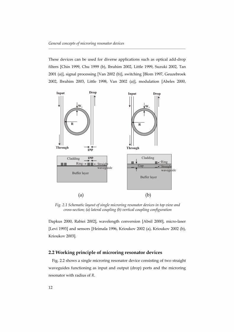
In general, a microring resonator device functioning as an optical filter
consists of two straight waveguide ports with a microring resonator in
between, which can be arranged in a lateral or vertical coupling configuration
as depicted in Fig. 2.1. Microring resonator devices can be composed by single
ring or multiple rings (in serial or parallel configuration).
General concepts of microring resonator devices _______________________________________________________________________________________
12
These devices can be used for diverse applications such as optical add-drop
filters [Chin 1999, Chu 1999 (b), Ibrahim 2002, Little 1999, Suzuki 2002, Tan
2001 (a)], signal processing [Van 2002 (b)], switching [Blom 1997, Geuzebroek
2002, Ibrahim 2003, Little 1998, Van 2002 (a)], modulation [Abeles 2000,
Dapkus 2000, Rabiei 2002], wavelength conversion [Absil 2000], micro-laser
[Levi 1993] and sensors [Heimala 1996, Krioukov 2002 (a), Krioukov 2002 (b),
Krioukov 2003].
2.2 Working principle of microring resonator devices Fig. 2.2 shows a single microring resonator device consisting of two straight
waveguides functioning as input and output (drop) ports and the microring
resonator with radius of R.
(a) (b)
Fig. 2.1 Schematic layout of single microring resonator devices in top view and cross-section; (a) lateral coupling (b) vertical coupling configuration
Through
Input
Through
Drop
W2
R
Buffer layer
Straightwaveguide
GapRing
Cladding
Input Drop
W2
R
Buffer layer
CladdingRing Straight
waveguide
gap
gap
Chapter 2 _______________________________________________________________________________________
13
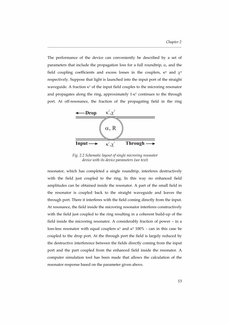
The performance of the device can conveniently be described by a set of
parameters that include the propagation loss for a full roundtrip, α, and the
field coupling coefficients and excess losses in the couplers, κn and χn
respectively. Suppose that light is launched into the input port of the straight
waveguide. A fraction κ1 of the input field couples to the microring resonator
and propagates along the ring, approximately 1-κ1 continues to the through
port. At off-resonance, the fraction of the propagating field in the ring
resonator, which has completed a single roundtrip, interferes destructively
with the field just coupled to the ring. In this way no enhanced field
amplitudes can be obtained inside the resonator. A part of the small field in
the resonator is coupled back to the straight waveguide and leaves the
through port. There it interferes with the field coming directly from the input.
At resonance, the field inside the microring resonator interferes constructively
with the field just coupled to the ring resulting in a coherent build-up of the
field inside the microring resonator. A considerably fraction of power – in a
loss-less resonator with equal couplers κ1 and κ2 100% - can in this case be
coupled to the drop port. At the through port the field is largely reduced by
the destructive interference between the fields directly coming from the input
port and the part coupled from the enhanced field inside the resonator. A
computer simulation tool has been made that allows the calculation of the
resonator response based on the parameter given above.
Fig. 2.2 Schematic layout of single microring resonator device with its device parameters (see text)
κ ,χ1 1
κ ,χ2 2
α, R α , 2 2R
Input Through
Drop
General concepts of microring resonator devices _______________________________________________________________________________________
14
On the other hand, by using the simulation model to fit experimental spectra
obtained with a resonator, ‘experimental’ values for these parameters can be
derived.
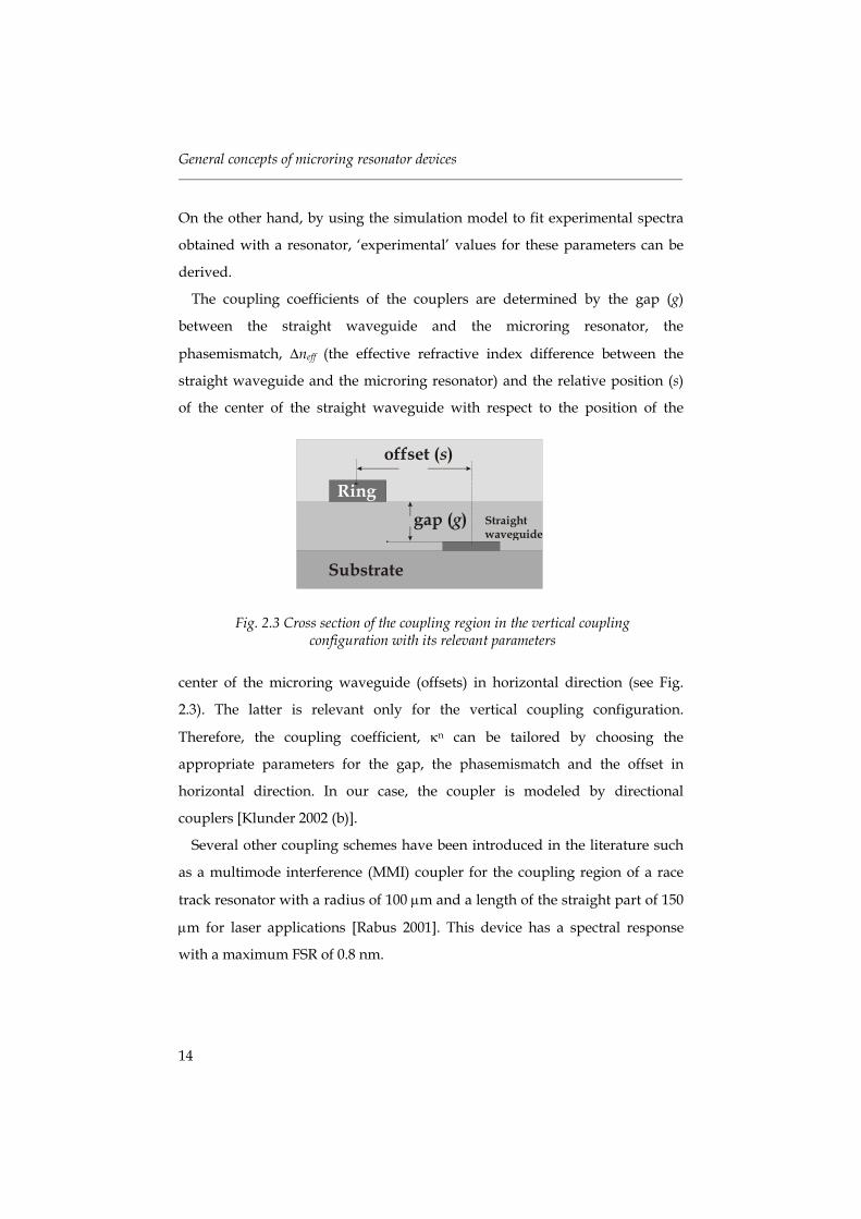
The coupling coefficients of the couplers are determined by the gap (g)
between the straight waveguide and the microring resonator, the
phasemismatch, ∆neff (the effective refractive index difference between the
straight waveguide and the microring resonator) and the relative position (s)
of the center of the straight waveguide with respect to the position of the
center of the microring waveguide (offsets) in horizontal direction (see Fig.
2.3). The latter is relevant only for the vertical coupling configuration.
Therefore, the coupling coefficient, κn can be tailored by choosing the
appropriate parameters for the gap, the phasemismatch and the offset in
horizontal direction. In our case, the coupler is modeled by directional
couplers [Klunder 2002 (b)].
Several other coupling schemes have been introduced in the literature such
as a multimode interference (MMI) coupler for the coupling region of a race
track resonator with a radius of 100 µm and a length of the straight part of 150
µm for laser applications [Rabus 2001]. This device has a spectral response
with a maximum FSR of 0.8 nm.
Fig. 2.3 Cross section of the coupling region in the vertical coupling configuration with its relevant parameters
gap ( )g
offset ( )s
Substrate
Straightwaveguide
Ring
Chapter 2 _______________________________________________________________________________________
15
Race-track based directional couplers have been fabricated [Chin 1999] by
using e-beam lithography in combination with deep etching using inductively
coupled plasma reactive ion etching (ICP-RIE), where very small ring radius
(cavity length of 31 µm, straight section in the coupling region of 6 µm) and
very narrow gap down to 200 nm are allowed.
2.3 The lateral and vertical coupling configuration In the following the two basic coupling schemes, lateral and vertical
coupling will be discussed in detail. Also design aspects and fabrication issues
will be presented.
2.3.1 The lateral coupling configuration In the lateral coupling configuration for microring resonator devices the
port waveguide(s) are structured in the same layer stack as the
microresonator. Coupling then is controlled by the horizontal gap between
microring and port waveguide (see Fig. 2.1a). The fabrication processes of this
device can be made very simple as a single mask process can be applied. This
configuration, however, misses flexibility as the straight waveguide and the
microring resonator can not be optimized individually.
The main problem in the lateral coupling configuration is the precise
structuring of the gap (see Fig. 2.1a) that depending on the materials system
can vary between 150 –1000 nm with an accuracy needed of better than 10%.
Conventional optical photolithography as applied in our case is only able to
open a gap of 750 nm or more. A gap of 500 nm could not be opened even if
we worked with a high-resolution e-beam mask for patterning. A good gap
definition in the lateral coupling configuration therefore is rather difficult to be
obtained. After our initial experiences with laterally coupled devices (see Ch.
3) we changed to the vertical coupling configuration (see Ch. 4).
General concepts of microring resonator devices _______________________________________________________________________________________
16
The main reason for this is that the coupling now is determined for a large
extent by the thickness of the separation layer, which can be deposited with
accuracy better than 10 nm.
2.3.2 The vertical coupling configuration In the vertical coupling configuration, the straight waveguides and the
microring resonators are etched in different layers (see Fig. 2.1b). From the
design point of view, this means increased flexibility because ring and port
waveguides can be optimized separately. In practice, however, fabrication can
experience severe difficulties due to possible misalignment between port
waveguide and ring, especially if one uses the standard mask aligners (Karl
Süss or EVG 620) that are available in the MESA+ clean room with a resolution
not much better than 500 nm. A lot of effort and much attention have been put
to minimize the misalignment problem. This problem can be solved only when
a mask aligner with a higher resolution or a waferstepper become available.
In the vertical coupling configuration, the thickness of the port waveguide
should be minimized to avoid planarization problems. By using a relatively
high refractive index material such as LPCVD Si3N4 the thickness can be
restricted to 140 nm. Another option is to apply Chemical Mechanical
Polishing (CMP) to planarize the gap layer. This process, however, is rather
difficult to be controlled on a nanometer scale, which results in a not well
defined gap thickness.
The microring resonator core can be made of LPCVD Si3N4 that has a
maximum thickness of approximately 300 nm or PECVD SiON with a
‘maximum’ refractive index of 1.65. The latter demands a thicker layer in the
order of 1.5 µm because of its relatively low refractive index. A PECVD SiON
layer with a refractive index of more than 1.65 is not recommended because it
will introduce some technical problems such as contamination of the
deposition chamber or, more important, cracking of the layer when an
annealing step is applied [Albers 1995].
Chapter 2 _______________________________________________________________________________________
17
2.4 Cascaded multiple microring resonator devices Microring resonator devices can consist of a single microring or cascaded
multiple microrings in either the lateral or vertical coupling configuration. Fig.
2.2 shows a single microring resonator device in the vertical coupling
configuration. These devices have shown promising functionality as filters (see
also Ch. 4 and Ch. 5). A specially tailored filter response with an increased
performance as needed in applications such as bandpass filter, spectral slicer,
(de)multiplexer can be obtained by cascading multiple microring resonators
and choosing the appropriate parameters (see also Ch. 6). Cascaded multiple
ring resonator devices can be arranged in a serial or parallel configuration. In
the following, both configurations will be discussed and explained in detail.
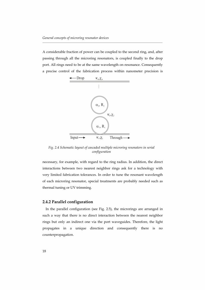
2.4.1 Serial configuration Fig. 2.4 shows the schematic layout of cascaded multiple microring
resonators in a serial configuration. Several microrings are positioned between
the input and the output port of the straight waveguides. The coupling
between the straight waveguides and the microring resonators and between
two microring resonators is modeled by directional couplers with coupling
coefficients, κn and excess losses in the coupler, χn. The propagation loss inside
the microring resonator and the microring radius are indicated by αn and Rn
respectively.
Light is launched from the input port (see Fig. 2.4) and couples in part to the
first microring. At off-resonance, the fraction of light, which has completed a
single roundtrip, interferes destructively with the light that has just coupled to
the ring. There is no build-up of the power inside the resonator. Only a small
amount of light is coupled to the second ring. The light remains mainly in the
straight waveguides and propagates to the through port. At on-resonance, the
fraction of light that has just completed one roundtrip in the first ring,
interferes constructively with the light that has just coupled to the ring
resulting in a coherent build-up of the power inside the microring resonator.
General concepts of microring resonator devices _______________________________________________________________________________________
18
A considerable fraction of power can be coupled to the second ring, and, after
passing through all the microring resonators, is coupled finally to the drop
port. All rings need to be at the same wavelength on resonance. Consequently
a precise control of the fabrication process within nanometer precision is
necessary, for example, with regard to the ring radius. In addition, the direct
interactions between two nearest neighbor rings ask for a technology with
very limited fabrication tolerances. In order to tune the resonant wavelength
of each microring resonator, special treatments are probably needed such as
thermal tuning or UV trimming.
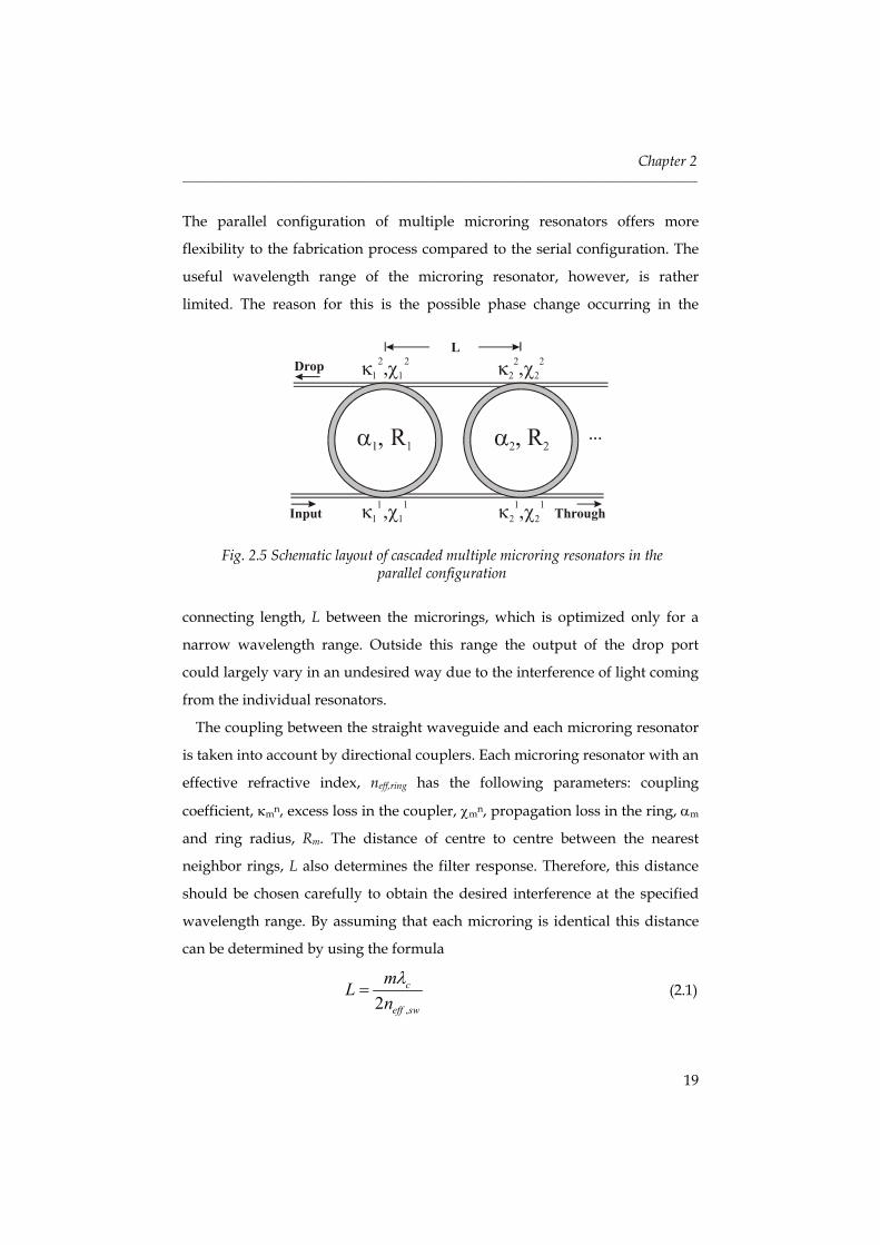
2.4.2 Parallel configuration In the parallel configuration (see Fig. 2.5), the microrings are arranged in
such a way that there is no direct interaction between the nearest neighbor
rings but only an indirect one via the port waveguides. Therefore, the light
propagates in a unique direction and consequently there is no
counterpropagation.
Fig. 2.4 Schematic layout of cascaded multiple microring resonators in serial configuration
κ χ1, 1
κ χ2 2,
κ χn n,
α1, R1
α , 2 2R
Input Through
Drop
…
Chapter 2 _______________________________________________________________________________________
19
The parallel configuration of multiple microring resonators offers more
flexibility to the fabrication process compared to the serial configuration. The
useful wavelength range of the microring resonator, however, is rather
limited. The reason for this is the possible phase change occurring in the
connecting length, L between the microrings, which is optimized only for a
narrow wavelength range. Outside this range the output of the drop port
could largely vary in an undesired way due to the interference of light coming
from the individual resonators.
The coupling between the straight waveguide and each microring resonator
is taken into account by directional couplers. Each microring resonator with an
effective refractive index, neff,ring has the following parameters: coupling
coefficient, κmn, excess loss in the coupler, χmn, propagation loss in the ring, αm
and ring radius, Rm. The distance of centre to centre between the nearest
neighbor rings, L also determines the filter response. Therefore, this distance
should be chosen carefully to obtain the desired interference at the specified
wavelength range. By assuming that each microring is identical this distance
can be determined by using the formula
,2c
eff sw
mLn
λ= (2.1)
Fig. 2.5 Schematic layout of cascaded multiple microring resonators in the parallel configuration
κ χ1 11 1,
κ χ1 12 2,
Input Through
Drop
…
L
General concepts of microring resonator devices _______________________________________________________________________________________
20
In this formula, m is an integer, cλ is the resonant wavelength, and ,eff swn is
the effective refractive index of the straight waveguides. When optimizing the
filter design for the desired wavelength response, L should be varied just as
any of the other parameters. Besides enabling the proper phase relation, the
distance L should be set to be large enough to avoid any direct interaction
between the neighboring rings.
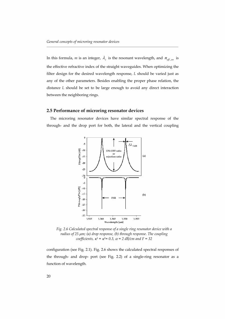
2.5 Performance of microring resonator devices The microring resonator devices have similar spectral response of the
through- and the drop port for both, the lateral and the vertical coupling
configuration (see Fig. 2.1). Fig. 2.6 shows the calculated spectral responses of
the through- and drop- port (see Fig. 2.2) of a single-ring resonator as a
function of wavelength.
Fig. 2.6 Calculated spectral response of a single ring resonator device with a radius of 25 µm; (a) drop response, (b) through response. The coupling
coefficients, κ1 = κ2= 0.3, α = 2 dB/cm and F = 32
FSR
∆λ-3dB
ON-OFF ratioor
rejection ratio (a)
(b)
Chapter 2 _______________________________________________________________________________________
21
By assuming that there is no coupling loss, the modal amplitude at the
through port and the drop port of a single-ring device are given by the
following expressions:
max(1)0
1 exp( ( )) 1through q
qinput q q c
A at
A b jk λ λ=
= −− − −∑ (2.2)
and ,max
1 exp( ( )) 1drop q
qinput q q c
A aA b jk λ λ=
= −− − −∑ (2.3)
where λc is a central wavelength, kq is related to the FSR by kq = 2π/FSRq; ρ is
the roundtrip phase shift, q is the mode number of the radial ring resonator
modes; t0(1) is related to the coupled fraction between straight waveguide and
ring resonator modes at the input straight waveguide; aq and aq’ are related to
the coupled fields and bq represents a phase term. The detailed derivation of
these equations and full definition of parameters can be found in [Klunder
2002 (b)]. The free spectral range, FSR is given by
2
2c
eff eff
FSRN Rλ
π= (2.4)
where λc is the resonant wavelength, effN is the effective refractive index of
the microring resonator mode, and effR is the effective radius of the microring
resonator mode. The finesse of the resonator, F, is defined by the following
relation
3dB
FSRFλ−
=∆
(2.5)
where 3dBλ−∆ is the bandwidth at -3 dB.
General concepts of microring resonator devices _______________________________________________________________________________________
22
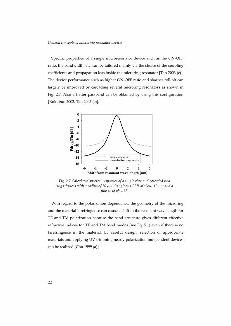
Specific properties of a single microresonator device such as the ON-OFF
ratio, the bandwidth, etc. can be tailored mainly via the choice of the coupling
coefficients and propagation loss inside the microring resonator [Tan 2003 (c)].
The device performance such as higher ON-OFF ratio and sharper roll-off can
largely be improved by cascading several microring resonators as shown in
Fig. 2.7. Also a flatter passband can be obtained by using this configuration
[Kokubun 2002, Tan 2003 (e)].
With regard to the polarization dependence, the geometry of the microring
and the material birefringence can cause a shift in the resonant wavelength for
TE and TM polarization because the bend structure gives different effective
refractive indices for TE and TM bend modes (see Eq. 5.1) even if there is no
birefringence in the material. By careful design, selection of appropriate
materials and applying UV-trimming nearly polarization independent devices
can be realized [Chu 1999 (a)].
Fig. 2.7 Calculated spectral responses of a single ring and cascaded two rings devices with a radius of 20 µm that gives a FSR of about 10 nm and a
finesse of about 5
Shift from resonant wavelength [nm]-6 -4 -2 0 2 4 6
Pdro
p/Pi
n [d
B]
-16
-14
-12
-10
-8
-6
-4
-2
0
Single ring deviceCascaded two rings device
Chapter 2 _______________________________________________________________________________________
23
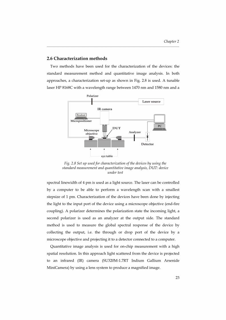
2.6 Characterization methods Two methods have been used for the characterization of the devices: the
standard measurement method and quantitative image analysis. In both
approaches, a characterization set-up as shown in Fig. 2.8 is used. A tunable
laser HP 8168C with a wavelength range between 1470 nm and 1580 nm and a
spectral linewidth of 4 pm is used as a light source. The laser can be controlled
by a computer to be able to perform a wavelength scan with a smallest
stepsize of 1 pm. Characterization of the devices have been done by injecting
the light to the input port of the device using a microscope objective (end-fire
coupling). A polarizer determines the polarization state the incoming light, a
second polarizer is used as an analyzer at the output side. The standard
method is used to measure the global spectral response of the device by
collecting the output, i.e. the through or drop port of the device by a
microscope objective and projecting it to a detector connected to a computer.
Quantitative image analysis is used for on-chip measurement with a high
spatial resolution. In this approach light scattered from the device is projected
to an infrared (IR) camera (SU320M-1.7RT Indium Gallium Arsenide
MiniCamera) by using a lens system to produce a magnified image.
Fig. 2.8 Set up used for characterization of the devices by using the standard measurement and quantitative image analysis, DUT: device
under test
Microscopeobjective
xyz table
Detector
Polarizer
PC
IR camera
Analyzer
Micropositioner
Readout
General concepts of microring resonator devices _______________________________________________________________________________________
24
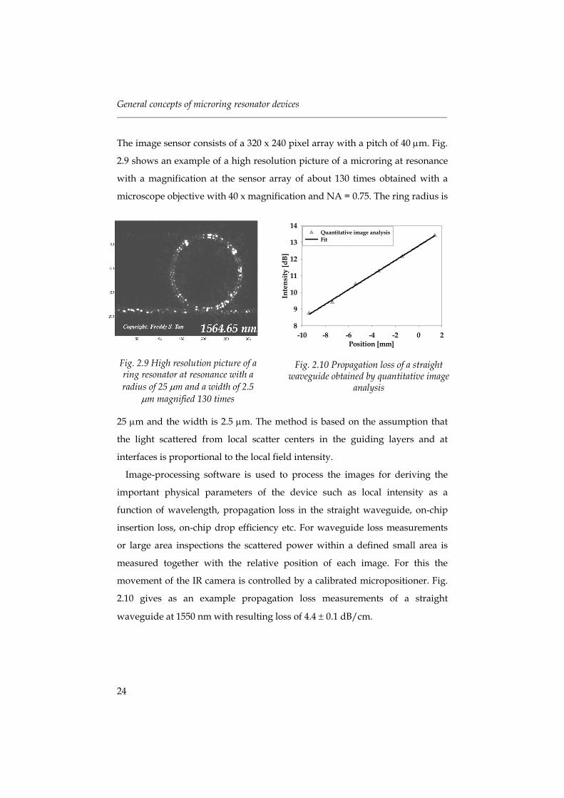
The image sensor consists of a 320 x 240 pixel array with a pitch of 40 µm. Fig.
2.9 shows an example of a high resolution picture of a microring at resonance
with a magnification at the sensor array of about 130 times obtained with a
microscope objective with 40 x magnification and NA = 0.75. The ring radius is
25 µm and the width is 2.5 µm. The method is based on the assumption that
the light scattered from local scatter centers in the guiding layers and at
interfaces is proportional to the local field intensity.
Image-processing software is used to process the images for deriving the
important physical parameters of the device such as local intensity as a
function of wavelength, propagation loss in the straight waveguide, on-chip
insertion loss, on-chip drop efficiency etc. For waveguide loss measurements
or large area inspections the scattered power within a defined small area is
measured together with the relative position of each image. For this the
movement of the IR camera is controlled by a calibrated micropositioner. Fig.
2.10 gives as an example propagation loss measurements of a straight
waveguide at 1550 nm with resulting loss of 4.4 ± 0.1 dB/cm.
Fig. 2.10 Propagation loss of a straight waveguide obtained by quantitative image
analysis
Position [mm]-10 -8 -6 -4 -2 0 2
Inte
nsity
[dB]
8
9
10
11
12
13
14Quantitative image analysisFit
Fig. 2.9 High resolution picture of a ring resonator at resonance with a radius of 25 µm and a width of 2.5
µm magnified 130 times
Chapter 2 _______________________________________________________________________________________
25
Conclusions Microring resonators are promising devices that offer high wavelength
selectivity in combination with an extremely small size that enables an
integration density of up to 105 devices per square centimeter.
Single and multiple microring devices can be implemented in structures
where the port waveguides are laterally or alternatively vertically coupled to
the microrings. For our applications and with the current technological
equipment the vertical coupling configuration is the best choice as only in this
configuration the straight waveguide and ring resonator can be optimized
individually. Besides that, in the fabrication process, vertical coupling is more
tolerant to the variation in technology than lateral coupling.
In the case of cascaded devices, the parallel configuration is more attractive
than serial one as the filter response obtained from the drop port can be
adjusted by varying the centre to centre distance of the nearest neighbor rings.
Two characterization methods have been used to evaluate the performance of
our devices, the standard measurement method that can be used for global
spectral measurements at the port waveguides and quantitative images
analysis. The latter provides precise information on the local light intensity at
any place of the device with a spatial resolution of better than 2 µm and a
spectral resolution determined by the linewidth of the tunable laser source (4
pm).

General concepts of microring resonator devices _______________________________________________________________________________________
26
Chapter 3 _______________________________________________________________________________________
27
Chapter 3
Design strategy
The general goal of this thesis is to elaborate new microresonator based
optical filter structures resulting in a realistic design and eventually to realize
demonstrator devices. In order to reach these objectives a design strategy has
been set up, see Fig. 3.1. It is a complex scheme with a number of input fields
to the design, intermediate action boxes, the final demonstrator device and
many interaction lines that include feedback at any of the intermediate stages.
In the following this scheme will be explained in some detail.
3.1 Input fields for the design activity Before starting with the actual design activity the objectives, available
knowledge and facilities and other boundary conditions have to be analyzed.
Also the position of the devices in a communication system has to be
considered.
3.1.1 Knowledge The first input field for the design is related to the knowledge base available
to this work composed by open literature and own understanding obtained in
our group or in collaboration with partners. At the beginning of the project
described in this thesis only a few groups were working in microring
resonator devices that were pioneered by Blom et al. [Blom 1996, Blom 1997]
and Little in 1997 [Little 1997]. Since that time, a lot of studies have been
carried out not only theoretically and numerically but also experimentally for
diverse applications. Also the number of groups working in this field has
largely been enhanced.
Design strategy _______________________________________________________________________________________
28
Each group is working on a peculiar class of devices as, depending on the
application, ring resonators can be realized in diverse materials systems such
as low refractive index contrast SiON/SiO2, high refractive index SiON or
Si3N4 in combination with SiO2 substrate, glass compound Ta2O5/SiO2 and
very high refractive index contrast material like Si/SiO2 or III-V
semiconductors.
Fig. 3.1 General design strategy to achieve the objectives of the project
System specifications
DesignObjectives Time frame
Intermediate Characterizations
Realization
FunctionalCharacterizations
SystemEvaluations
Demonstratordevice
Technology and
facilities
Knowledge Previous Experiences
Design tools
Chapter 3 _______________________________________________________________________________________
29
In our group, high refractive index SiON or Si3N4 based structures in
combination with SiO2 substrates have been used. In a different project at the
IOMS group also polymer based devices for electro-optic modulation are
being developed [Leinse 2003]. In the course of the current study the
knowledge basis has largely increased. This is reflected among others in the
increasing complexity and performance of the devices like the spectral slicers
of chapter 7. A good overview demonstrating the current status in the field has
been presented in a recent Summerschool at Erice organized by the NAIS
project [Bertolotti 2004]. The presentations of the invited talks can be found at
the NAIS Website [NAIS Website].
3.1.2 Previous experiences Probably the most important input field for the design activities is the
previous experience that, being in certain aspects a specific subset of
“knowledge”, exceeds it largely. It includes the many unwritten rules and
unpublished and not for publication suitable results obtained by own effort or
by informal discussion. In this respect, transfer of knowledge from previous
PhD students in our group who were also working in the field of
microresonators is the most important contribution. The first PhD student who
had been working in this field is F. Blom (1996-1998). He has introduced as a
pioneer the microresonator in our group and was one of the first with a
publication on a working device [Blom 1998, Blom 1997]. His objective was to
demonstrate all-optical switching by field enhancement. Disk and ring
resonators have been realized with Si3N4/SiO2 technology in combination with
AKZO-DANS polymer by using a very basic technology. The results were
promising, but all-optical switching could not be demonstrated
experimentally. In a collaboration with another MESA+ group extended
scanning nearfield optical microscopy (SNOM) pictures of one of his devices
could be obtained revealing a rich spectrum of optical phenomena [Balistreri
2001, Klunder 2000 (a)].
Design strategy _______________________________________________________________________________________
30
A second PhD student at IOMS who was working in the field had been D.J.W
Klunder (1998-2002) who explored experimentally and theoretically high
finesse microresonators, mainly made in Si3N4/SiO2 technology. In
collaborations within IOMS and other MESA+ groups and later also with the
NAIS project he deepened the understanding of microresonators and worked
on new applications in the field of optical communication, optical sensing and
stimulated emission. Another Ph.D student, C.G.H. Roeloffzen (1998-2002)
had been working on optical filters for WDM applications on the basis of SiON
waveguides that included relatively small FSR ring resonators.
The national BTS project (1999-2001) resulted in valuable experience for ring
resonator devices for application in WDM networks. With the European NAIS
project (2001-2004) the number of people involved was largely extended and
progress has been made in all fields relevant for the successful realization of
microring devices, see Ch. 1 for more detail. The experience accumulated at
the end of this project and thereafter being available to the current design
activities has augmented largely. As a consequence tasks that only a few years
ago were considered to be very challenging are meanwhile routinely carried
out.
3.1.3 Design tools In order to be able to design the devices, software by two companies are
available in our group: Concept to Volume (C2V) and FEMLAB. The C2V
software called Selene and Olympios is more suitable for our purposes and
better known in our group. Selene Stress and Temperature software is a two-
dimensional mode solver that calculates the effective refractive index of the
quasi-TE and TM modes in the port waveguide. In the case of the bend solver,
it calculates also the bending loss of the quasi-TE and TM of the bend modes.
Chapter 3 _______________________________________________________________________________________
31
The Olympios packet simulates mode propagation in the waveguide by using
the two- and three-dimensional Beam Propagation Method (BPM) or two-
dimensional Bi-directional Eigenmode Propagation (BEP) and can also be used
for masks design. Simulations of ring resonator devices by using Olympios
with BPM can only give qualitative trends because of the limitation of this
method. In the two-dimensional case, the BEP method is more reliable than
BPM because reflection and optical feedback can be taken into account.
However, in the case of a vertical coupling configuration, BEP is not able to
deal with three dimensions and does consequently not provide a realistic
design, for example of coupling coefficients. Therefore a fully three-
dimensional design tool is strictly necessary to obtain reliable and accurate
results.
Besides the commercial tools a number of codes have been developed in this
work and by others [Tan/Klunder 2002, Tan 2003 (d)]. Klunder has developed
an analytical model of the response of single cylindrical microresonator in
term of modal amplitudes of the straight waveguide and the microresonator
modes by using scattering matrix approach for the analysis of the response
obtained from the through port [Klunder 2002 (b)]. In this model several
assumptions have been made: the straight waveguide is single mode, the
resonator modes are propagating in one direction, the evanescent field
coupling can be modeled as an abrupt process at a certain reference plane, no
mode conversion and no input signal from the add port etc. This simulation
model has been further worked out [Tan/ Klunder 2002] to allow the analysis
of the response of single ring devices obtained at the drop port, which is more
important for our project. Recently, this model has also been extended to be
able to analyze the response of cascaded multiple ring devices obtained at the
drop port [Tan 2003 (d)]. These simulation models can be fitted to the
experimental data obtained from measurements to derive its physical
parameters such as coupling coefficients, propagation loss etc.
Design strategy _______________________________________________________________________________________
32
Besides the simulation tools developed in our group, detailed analytical and
numerical studies have been carried out by the Applied Analysis and
Mathematical Physics (AAMP) Group, MESA+, University of Twente and the
Institute of Radio Engineering and Electronics (IREE) who as partners of the
NIAS project deal with theoretical aspects of microresonators. As a result, the
AAMP was able to develop a numerical tool that calculates the coupling
coefficients by using a simplified coupled mode theory [Hammer 2003]. The
IREE developed a fully three-dimensional mode solver that determines the
bend modes
3.1.4 Technology and facilities Technological limitations and availability of the facilities also influence our
design. The application of SiON in our group has been motivated by its
excellent optical properties such as low absorption in the visible and near
infrared wavelength range. Moreover, the refractive index of SiON can also
easily be adjusted over a large range between 1.45 (SiO2) to 2.0 (Si3N4). In
addition, standard silicon substrates can be used and reliable techniques that
are compatible with standard silicon integrated circuit processing are
available. Conventional optical photolithography by using contact printing
and standard etching processes such as wet etching and dry etching (e.g. RIE)
are available in our MESA+ clean room. This approach opens a route for
potentially low-cost mass production. Another technological issue is the
minimum dimensions of structures that can be written on the mask. The Laser
Mask Generator (Heidelberg Instrument DWL 2.0) that is available in the
MESA+ clean room can manufacture masks with structures with a smallest
dimension of 2 µm. On the other hand, high-resolution e-beam masks can
realize structures down to 100 nm without any problems.
Chapter 3 _______________________________________________________________________________________
33
When we apply conventional optical photolithography with the aid of contact
printing, a technique available in the MESA+ clean room, the use of a high-
resolution e-beam mask for structures with dimension not smaller than 2 µm is
not a meaningful and cost-effective option. Therefore optimizing the design to
structures with smallest dimension not less than 2 µm could allow writing
low-cost masks in the MESA+ clean room. High-resolution e-beam masks, or
the application of a waferstepper with 4 or 5 times reduction, would allow
producing structures with smoother surface sidewalls and consequently
reduced scattering loss as the roughness on the masks will be transferred
directly to the resist pattern.
3.1.5 Objectives Another important input to the design are the objectives of the project. They
are closely related to the objectives of the two projects the work in this thesis
made part of. In both projects the microresonator based devices were intended
for the access network and consequently should be low-cost. Besides that
operation in an every-day and common environment should be possible
without the need of maintenance by trained engineers. In addition the devices
should demonstrate the use of microresonators as building block for VLSI
photonics. For this, issues as on-chip insertion loss, waferscale reproducibility,
and also the introduction of increasing complexity are of primary importance.
To meet the demand on potentially low-cost fabrication our devices have been
designed for high refractive index SiON/ SiO2 or Si3N4/ SiO2 in combination
with available conventional technology. By using these materials and
technology, the ring radius can be reduced down to 10 - 30 µm corresponding
to a FSR of about 20 nm - 8 nm. This range can in some cases be extended by
Vernier-type multi-ring devices allowing meaningful applications in the
proposed access networks.
Design strategy _______________________________________________________________________________________
34
3.1.6 Time frame The design activities are also limited by the time frame given by the projects
and their deliverables and milestones. The two years of the BTS project
allowed only for a few design iterations, as in that time the knowledge,
previous experience and man-power involved was quite restricted. The still
continuing NAIS project (2001-2004) could count with much better starting
conditions and largely increased man-power. The milestones and deliverables,
however, were much more demanding and asked for specific activities: work
on multi-ring devices and build up of a characterization set-up with high
spatial resolution. The number of device iterations within NAIS was high and
related to deliverables. Chapter 6 and 7 reflect the most important results.
Another time frame is of course the fulfillment of the academic demands of a
Ph.D. thesis with an individually traceable contribution of the Ph.D. candidate
in question. Especially in the NAIS project a team of 5 Ph.D. students have
been or are currently involved with different overlap in time. This, of course is
of great benefit for transfer of knowledge, but puts special demands on
publications and reports.
3.1.7 System specifications For the projects involved, the system specifications such as insertion loss,
fiber to chip coupling loss, crosstalk etc. are of primary importance. In the BTS
the system concept was still quite open, in the NAIS project, however, a
specific application, a WDM transceiver module for the access network, has
been chosen.
Chapter 3 _______________________________________________________________________________________
35
For example, the responsible partner, Nortel gives the following general
requirements: a wavelength band in the range of 1530 – 1560 nm, a minimum
number of 16 wavelengths, a fiber span of 10 - 20 km, a transmission speed of
1.25 Gbit/s, an optical power budget (point to point) of minimum 6 dB due to
fiber loss, an optical power budget (Passive Optical Network, PON) of
minimum 20 dB due to fiber loss and passive splitter (assume PON
architecture with passive splitter loss of 14 dB for 16 way) and finally, a cost
limit of US$ 200 for a complete transceiver. For a bit-rate of 1.25 Gbit/s the
roundtrip time should be less than a few ps. Accordingly the ring radius
should not exceed 50 µm.
3.2 Field of specific activities
3.2.1 Design After having discussed the input fields, in the following the specific activity
fields will be explained in some details. In the design process first the
functional performance has to be considered as given by the system
specifications and objectives. Considering the requirements of the system of at
least 16 wavelengths we should provide a FSR of more than 20 nm. At this
moment our devices with the smallest ring radius of 15 µm have a FSR of
about 14 nm, substantially lower than the expected minimum of 20 nm.
However, the FSR can largely be enhanced by using a two-ring approach in a
Vernier configuration [Griffel 2000 (a)].
After the first experiences with resonators in the lateral coupling
configuration the vertical arrangement has been chosen because of the better
controlled fabrication technology, see also Sec. 2.3.2. As the coupling
coefficients in the vertical coupling configuration are determined by the
phasemismatch, the thickness of the gap and the offsets in lateral direction a
precise definition of the gap is essential for well working devices, see also Sec.
2.2.
Design strategy _______________________________________________________________________________________
36
A low enough phasemismatch is obtained by optimizing the effective
refractive index difference of the port waveguide and the ring using available
software [C2V]. In the design procedure first the effective index of the ring
that allows a sufficient low bending loss is calculated. Thereafter a port
waveguide with approximately the same effective index is designed with the
restriction that it should be single mode at the minimum width allowed by our
current lithography (~ 2 µm). In the previous work on resonators with the
vertical coupling configuration the coupling coefficients have been estimated
experimentally, by fitting the simulation model to the spectral response
obtained by the experiment. Our result then was that a gap of about 1 µm will
give a field coupling coefficients between 0.4 – 0.6. Currently, however, the
coupling coefficients can now be estimated numerically before the devices are
fabricated [Hammer 2003].
The first mask design has been done for 4” mask by using Olympios
software [C2V] to be able to use a complete area of a 3” wafer. A lot of ring
structures have been put on the ring mask such as single ring devices with
different ring radius and width, switch structures, etc. to be combined with an
appropriate waveguide mask for the port waveguide. Test structures were
also included like straight waveguides. Later on, due to the facilities available
in MESA+ clean room, only 5” masks have been used to be able to use a
complete area of a 4” wafer.
In this thesis filter devices are considered with increasingly specifically
tailored performance. In the beginning single ring devices were designed with
promising filter functionality. With the experiences obtained from single ring
devices we designed more complex devices by cascading multiple rings in
parallel arrangement. Their response show better performance than the
response obtained with single ring devices such as higher ON-OFF ratio,
flatter passband and lower crostalk. Finally, spectral slicer devices based on
single ring and cascaded two rings were designed and demonstrated for the
first time.
Chapter 3 _______________________________________________________________________________________
37
3.2.2 Realization After completing the design process, the realization step is started. As we
use the vertical coupling configuration covering the port waveguides with an
intermediate gap layer causes bumps on the layer stack. Even if the port
waveguides are very thin a not well-define profile of the gap layer is obtained.
In order to solve this problem, Chemical Mechanical Polishing (CMP) is
sometimes used for planarization. Another issue in the realization is that
inspection directly after the developing of the resist layer shows that
sometimes the rings can not be well aligned to the port waveguides.
Consequently the photolithographic process had to be repeated. Ideally one
would like to work with a mask aligner with a resolution better than 100
nanometers. Another aligning problem arises from the curvature of the wafer
due to the stress after deposition of the layer stack.
Since we have problem with the alignment of the two masks we decided to
use only a small area of 2 x 3 cm2 in the center part of the mask assuming that
the influence of the curvature on the wafer will probably be less for such a
small area. It appears that the use of a restricted wafer area does not resolve
the problem. However, some wafers consisting of several working devices
have successfully been fabricated and characterized. Their results are
presented in this thesis. Aligning problem due to the low resolution of the
mask aligner can probably be solved by utilizing a waferstepper with an
overlay accuracy of about 100 nm or growing a layer on both sides of the
wafer that might reduce the curvature effect on the wafer. Most of the devices
were processed by experienced technicians of the IOMS group, first G. Sengo
and L. Hilderink and later also H. Kelderman. Results from the realization
step have often been used as a feedback to the design activities.
3.2.3 Intermediate characterization Before we go to the functional characterizations of the devices, the
intermediate characterization has to be done.
Design strategy _______________________________________________________________________________________
38
This step is intended for preliminary characterization of the layer thickness,
refractive index, test of the lithography processes, etc. For the layer thickness
and refractive index measurements, there are two methods available in our
group; prism coupling and ellipsometry. The photolithographic process often
had to be repeated because observation of the alignment marks before etching
process shows that the rings were not well aligned with the respect to the port
waveguides. In one of our samples the intermediate characterization revealed
already a too thin layer. The devices, however, were completely processed and
analyzed nevertheless the high roundtrip losses of the resonators (see Ch. 6).
3.2.4 Functional characterization Functional characterization is intended to evaluate the functionality of the
device. In order to be able to evaluate the device performance, two
characterization set-up have been built during my PhD work, see also Sec 2.5;
a standard characterization set-up for global spectral measurements that has
been built and developed by using a former set-up available in our group
together with another PhD student and a completely new imaging set-up for
local measurements. This set-up provides precise information on the local
light intensity at every part of the devices with spatial resolution down to less
than 2 µm and has been built as fulfillment of a formal deliverable of
workpackage 5 of the NAIS project. The performance of this set-up has largely
improved after acquisition of an Infrared CCD camera that is sensitive for
wavelengths around 1.5 µm (SU320M-1.7RT Indium Gallium Arsenide
MiniCamera). The largely improved sensitivity (2-3 orders of magnitude)
allowed higher magnification and consequently larger resolution.
In order to be able to evaluate the device performance, comparison with a
simulation model has been made. This model has been made as close as
possible to the real situation of the device. The device parameters were not
fixed but allowed to vary freely. In this way the stability of our simulation
program against small variations could be examined.
Chapter 3 _______________________________________________________________________________________
39
After the fitting is completed, the simulated curve should be close to the
experimental spectral response and all device parameters such as coupling
coefficients, propagation loss inside the ring, effective radius of bend mode,
effective refractive index of the bend mode etc. can be obtained. The
simulation results can also be checked by using known parameters such as the
effective refractive index of the bend modes that can be calculated with Selene
Stress and Temperature of C2V. This simulation processes should be iterated
to obtain the best fit between the simulation model and the spectral response
with reasonable fitting parameters. The result from this analysis gives an
important feedback to the intermediate characterization step, the realization
step and the design step where necessary improvements and modifications
can be implemented.
3.2.5 System demonstrator When the evaluations show that the device response meets the
requirements, the next step is to combine all functional devices together to
build a system on a single chip. The system performance should also be
evaluated by comparing the results from the evaluations with the
specifications that have been determined in the beginning. These evaluation
results become an input for the previous steps. These steps might probably be
iterated several times to achieve the expected results that meet the system
requirements. When system specifications are fulfilled, therefore, we have a
demonstrator device.
Conclusions
The design strategy is a complex procedure to combine previous knowledge,
constraints from the system concept and availability of tools and facilities in an
innovative design. The design is verified by several fabrication and
characterization steps and results eventually in a demonstrator.

Design strategy _______________________________________________________________________________________
40
As constraints are changing and knowledge, facilities and experience
continuously improving, the design strategy involves numerous feedback
lines. In the course of this thesis an evolution from simple single microring to
complex multi-ring devices with an improved functionality could be realized.
Chapter 4 _______________________________________________________________________________________
41
Chapter 4
High finesse single-ring resonator devices based on a
lateral coupling configuration for WDM applications
The study of microring devices in our group has started with devices in the
lateral coupling configuration. In this arrangement, both the port waveguides
and the ring are located on the same layer. In order to minimize the bending
loss of the ring, we need relatively high refractive index materials. The Silicon
Oxynitride (SiON) technology [Wörhoff 1999, Wörhoff 2002], which is
extensively used in our group, allows a broad range of refractive indices
between 1.45 (SiO2) and 2.0 (Si3N4) and is appropriate for this purpose. By
using LPCVD Si3N4, the optimized dimensions of the ring are a radius of 25
µm and a width of 2.5 µm. The straight waveguide has a width of 1 µm. The
thickness of both, ring and waveguide is 300 nm that is limited by the
maximum thickness of Si3N4 layers achieved by the LPCVD process.
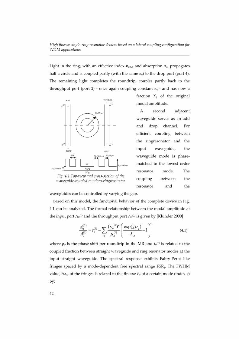
The standard measurement method [Tan 2003 (b)] has been used to
characterize the devices. For completeness, detail on-chip measurements based
on quantitative image analysis [Tan 2003 (b)] have also been done. A low on-
chip insertion loss of less than 0.2 dB could be measured [Tan 2001 (b)]. The
detailed experimental results of single ring devices in the lateral coupling
configuration using the standard measurement method have been reported in
[Tan 2001 (a)] and are presented in full in the following section.
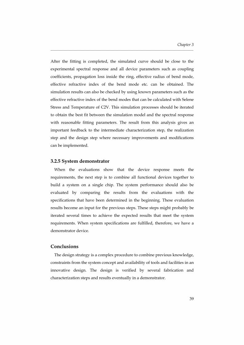
Design of a micro-ringresonator The layout of a microresonator is schematically given in Fig. 4.1. Light from
a single-mode input channel (port 1) is coupled partly (depending on the
coupling constant, κq) to the ringresonator, which supports several radial
modes. The remaining light will propagate to the throughput port (port 2).
High finesse single-ring resonator devices based on a lateral coupling configuration for WDM applications _______________________________________________________________________________________
42
Fig. 4.1 Top-view and cross-section of the waveguide-coupled to micro-ringresonator
Light in the ring, with an effective index neff,q and absorption αq, propagates
half a circle and is coupled partly (with the same κq) to the drop port (port 4).
The remaining light completes the roundtrip, couples partly back to the
throughput port (port 2) - once again coupling constant κq - and has now a
fraction Xq of the original
modal amplitude.
A second adjacent
waveguide serves as an add
and drop channel. For
efficient coupling between
the ringresonator and the
input waveguide, the
waveguide mode is phase-
matched to the lowest order
resonator mode. The
coupling between the
resonator and the
waveguides can be controlled by varying the gap.
Based on this model, the functional behavior of the complete device in Fig.
4.1 can be analyzed. The formal relationship between the modal amplitude at
the input port A0(1) and the throughput port A0(2) is given by [Klunder 2000]
1(1) 2(2)(1)00(1) (1)
0
( ) exp( )1q q
q q q
jA tA X
κ ρµ
−⎛ ⎞
= − −⎜ ⎟⎜ ⎟⎝ ⎠
∑ (4.1)
where ρq is the phase shift per roundtrip in the MR and t0(1) is related to the
coupled fraction between straight waveguide and ring resonator modes at the
input straight waveguide. The spectral response exhibits Fabry-Perot like
fringes spaced by a mode-dependent free spectral range FSRq. The FWHM
value, ∆λq, of the fringes is related to the finesse Fq of a certain mode (index q)
by:
Chapter 4 _______________________________________________________________________________________
43
FSRFλ
=∆
(4.2)
In our model the normalized spectral response at the drop and throughput
port of a symmetric micro-ringresonator is governed by only two parameters:
the roundtrip loss (RTL) and the coupling coefficient (κq).
Experimental results The devices were fabricated by LPCVD deposition of silicon nitride (n =
1.98) on a thermally oxidized silicon wafer [Wörhoff 1999]. Structuring was
done by standard optical lithography and RIE etching. A micro-ringresonator
with 750 nm gap has been characterized by launching TE polarized light of a
tunable laser diode into the input port of the waveguide and measuring the
power in the throughput port.
Fig. 4.3 shows the spectral response of the device in the range of 1510 to 1580
nm, which exhibits a slowly varying background level and the sharp
resonance peaks separated by the FSR. The reduced transmission of the
background at lower wavelengths is caused by the absorption of the SiON
material itself due to the incorporation of hydrogen during the deposition
process [Wörhoff 1999].
Wavelength [nm]Wavelength [nm]
Nor
mal
ized
thro
ugh
pow
er
Fig. 4.3 Enlargement of Fig. 4.2 around the resonance at 1510.25 nm. Besides the experimental data also a fit by our model
is given
Wavelength (nm)1520 1540 1560 158
Nor
mal
ized
thro
ughp
ut
0.2
0.4
0.6
0.8
1.0
1.2
Fig. 4.2 Measured power in the
throughput port of the micro-ring resonator for a gap of 750 nm
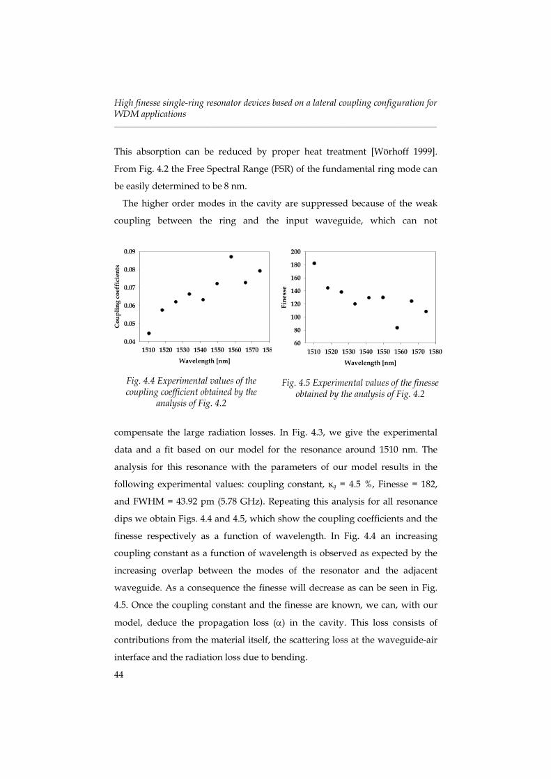
High finesse single-ring resonator devices based on a lateral coupling configuration for WDM applications _______________________________________________________________________________________
44
This absorption can be reduced by proper heat treatment [Wörhoff 1999].
From Fig. 4.2 the Free Spectral Range (FSR) of the fundamental ring mode can
be easily determined to be 8 nm.
The higher order modes in the cavity are suppressed because of the weak
coupling between the ring and the input waveguide, which can not
compensate the large radiation losses. In Fig. 4.3, we give the experimental
data and a fit based on our model for the resonance around 1510 nm. The
analysis for this resonance with the parameters of our model results in the
following experimental values: coupling constant, κq = 4.5 %, Finesse = 182,
and FWHM = 43.92 pm (5.78 GHz). Repeating this analysis for all resonance
dips we obtain Figs. 4.4 and 4.5, which show the coupling coefficients and the
finesse respectively as a function of wavelength. In Fig. 4.4 an increasing
coupling constant as a function of wavelength is observed as expected by the
increasing overlap between the modes of the resonator and the adjacent
waveguide. As a consequence the finesse will decrease as can be seen in Fig.
4.5. Once the coupling constant and the finesse are known, we can, with our
model, deduce the propagation loss (α) in the cavity. This loss consists of
contributions from the material itself, the scattering loss at the waveguide-air
interface and the radiation loss due to bending.
Wavelength [nm]1510 1520 1530 1540 1550 1560 1570 158
Cou
plin
g co
effi
cien
ts
0.04
0.05
0.06
0.07
0.08
0.09
Fig. 4.4 Experimental values of the coupling coefficient obtained by the
analysis of Fig. 4.2
Wavelength [nm]1510 1520 1530 1540 1550 1560 1570 1580
Fine
sse
60
80
100
120
140
160
180
200
Fig. 4.5 Experimental values of the finesse
obtained by the analysis of Fig. 4.2
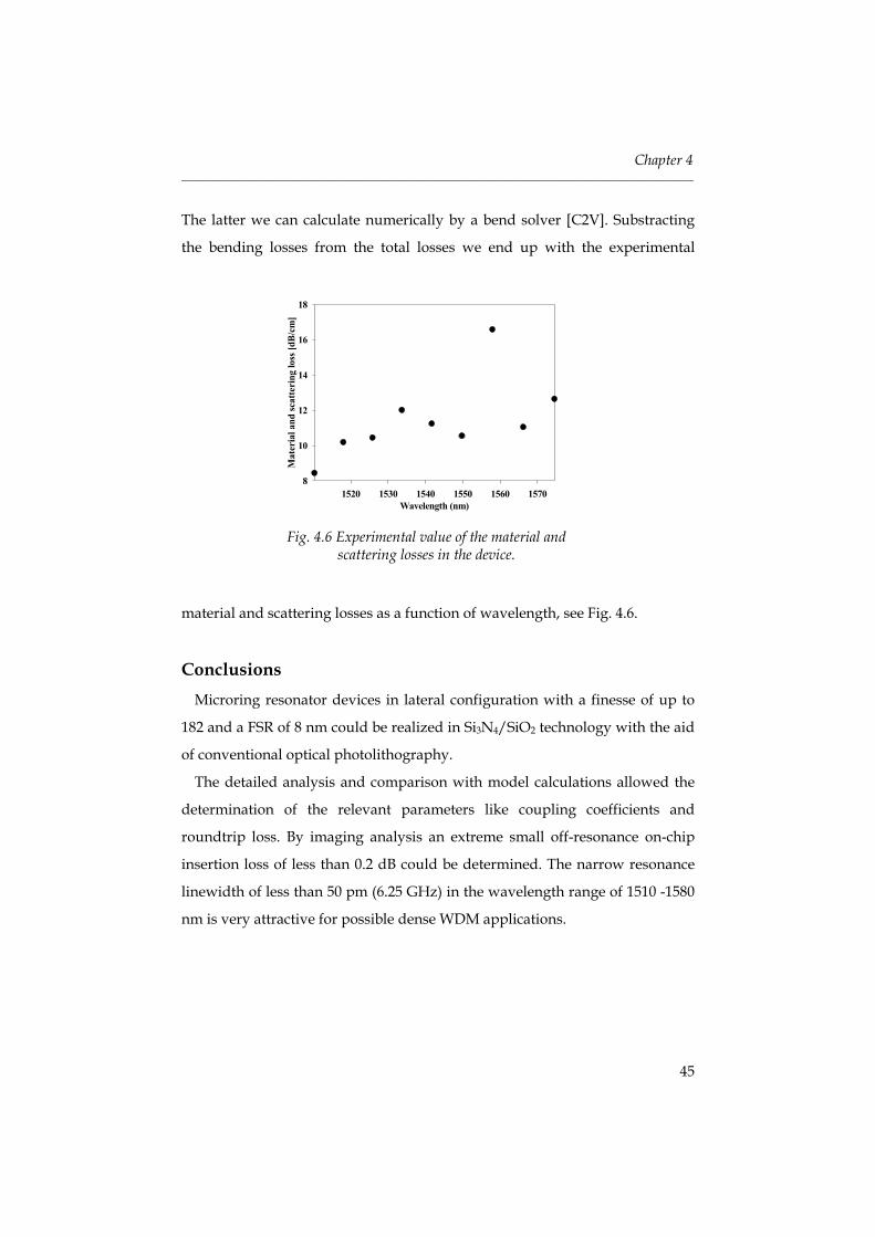
Chapter 4 _______________________________________________________________________________________
45
Wavelength (nm)1520 1530 1540 1550 1560 1570
Mat
eria
l and
scat
teri
ng lo
ss [d
B/c
m]
8
10
12
14
16
18
Fig. 4.6 Experimental value of the material and scattering losses in the device.
The latter we can calculate numerically by a bend solver [C2V]. Substracting
the bending losses from the total losses we end up with the experimental
material and scattering losses as a function of wavelength, see Fig. 4.6.
Conclusions Microring resonator devices in lateral configuration with a finesse of up to
182 and a FSR of 8 nm could be realized in Si3N4/SiO2 technology with the aid
of conventional optical photolithography.
The detailed analysis and comparison with model calculations allowed the
determination of the relevant parameters like coupling coefficients and
roundtrip loss. By imaging analysis an extreme small off-resonance on-chip
insertion loss of less than 0.2 dB could be determined. The narrow resonance
linewidth of less than 50 pm (6.25 GHz) in the wavelength range of 1510 -1580
nm is very attractive for possible dense WDM applications.

High finesse single-ring resonator devices based on a lateral coupling configuration for WDM applications _______________________________________________________________________________________
46
Chapter 5 _______________________________________________________________________________________
47
Chapter 5
Single microring resonator devices based on a vertical
coupling configuration
In this chapter, single microring resonator devices with a vertical coupling
configuration are discussed in detail. For the realization two alternatives have
been chosen where in both cases the port waveguides were made from Si3N4,
the microring core, however, etched either out of a SiON or a Si3N4 layer, see
Section 5.1 and 5.3 respectively. In the course of the work the quantitative
image analysis set-up has been developed and applied for the first time to the
devices described in Section 5.1. We include therefore in Section 5.2 a detailed
description of these results already published in [Tan 2003 (b)].
5.1 Silicon Oxynitride based microring resonator devices In our group the first results with microring resonators have been obtained
with devices with a lateral coupling configuration, see Chapter 4. These
devices were designed for TE polarization only. In this section, a feasibility
study of microring resonators for telecommunication applications within the
BTS project [BTS project] is presented. The proposed devices should work for
TE and TM polarization.
For the realization of the devices SiON technology has been chosen as the
large range of the index of refraction (1.45 – 2) provides large freedom in the
design. In the design process a balance has to be found between the refractive
index of the optical layers, the potential and limitations of the fabrication
process and the availability of materials. In this process detailed computer
simulations play a crucial role.
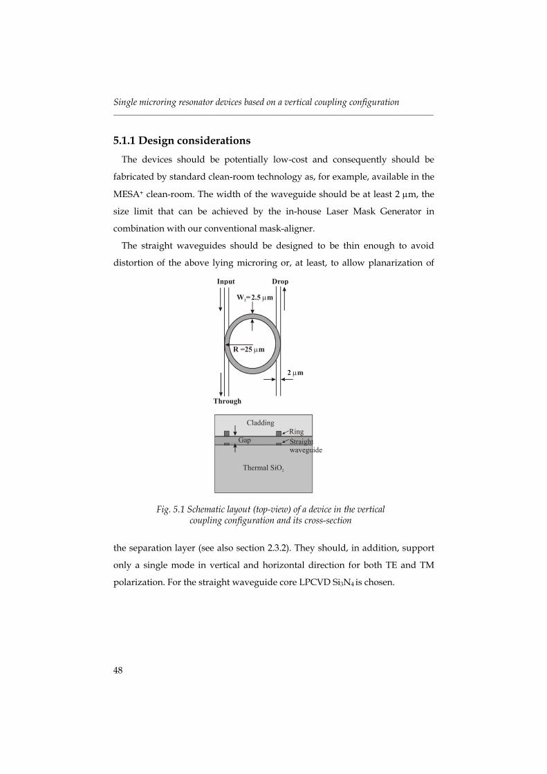
Single microring resonator devices based on a vertical coupling configuration _______________________________________________________________________________________
48
5.1.1 Design considerations The devices should be potentially low-cost and consequently should be
fabricated by standard clean-room technology as, for example, available in the
MESA+ clean-room. The width of the waveguide should be at least 2 µm, the
size limit that can be achieved by the in-house Laser Mask Generator in
combination with our conventional mask-aligner.
The straight waveguides should be designed to be thin enough to avoid
distortion of the above lying microring or, at least, to allow planarization of
the separation layer (see also section 2.3.2). They should, in addition, support
only a single mode in vertical and horizontal direction for both TE and TM
polarization. For the straight waveguide core LPCVD Si3N4 is chosen.
Fig. 5.1 Schematic layout (top-view) of a device in the vertical coupling configuration and its cross-section
Input
Through
Drop
W =2.5 m2 µ
R =25 m µ
Straightwaveguide
GapRing
Cladding
2 mµ
Thermal SiO2
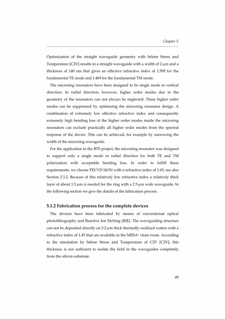
Chapter 5 _______________________________________________________________________________________
49
Optimization of the straight waveguide geometry with Selene Stress and
Temperature [C2V] results in a straight waveguide with a width of 2 µm and a
thickness of 140 nm that gives an effective refractive index of 1.509 for the
fundamental TE mode and 1.469 for the fundamental TM mode.
The microring resonators have been designed to be single mode in vertical
direction. In radial direction, however, higher order modes due to the
geometry of the resonators can not always be neglected. These higher order
modes can be suppressed by optimizing the microring resonator design. A
combination of extremely low effective refractive index and consequently
extremely high bending loss of the higher order modes inside the microring
resonators can exclude practically all higher order modes from the spectral
response of the device. This can be achieved, for example by narrowing the
width of the microring waveguide.
For the application in the BTS project, the microring resonator was designed
to support only a single mode in radial direction for both TE and TM
polarization with acceptable bending loss. In order to fulfill these
requirements, we choose PECVD SiON with a refractive index of 1.65, see also
Section 2.3.2. Because of this relatively low refractive index a relatively thick
layer of about 1.5 µm is needed for the ring with a 2.5 µm wide waveguide. In
the following section we give the details of the fabrication process.
5.1.2 Fabrication process for the complete devices The devices have been fabricated by means of conventional optical
photolithography and Reactive Ion Etching (RIE). The waveguiding structure
can not be deposited directly on 3.2 µm thick thermally oxidized wafers with a
refractive index of 1.45 that are available in the MESA+ clean room. According
to the simulation by Selene Stress and Temperature of C2V [C2V], this
thickness is not sufficient to isolate the field in the waveguides completely
from the silicon substrate.
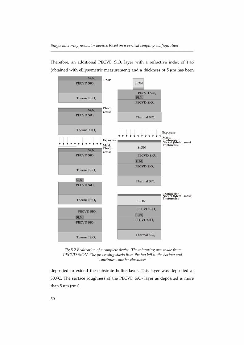
Single microring resonator devices based on a vertical coupling configuration _______________________________________________________________________________________
50
Therefore, an additional PECVD SiO2 layer with a refractive index of 1.46
(obtained with ellipsometric measurement) and a thickness of 5 µm has been
deposited to extend the substrate buffer layer. This layer was deposited at
3000C. The surface roughness of the PECVD SiO2 layer as deposited is more
than 5 nm (rms).
Fig.5.2 Realization of a complete device. The microring was made from PECVD SiON. The processing starts from the top left to the bottom and
continues counter clockwise
PECVD SiO2
Si N3 4
Thermal SiO2
PECVD SiO2
MaskExposure
Thermal SiO2
Si N3 4Photoresist
PECVD SiO2
Nickel (Metal mask)SiON
PECVD SiO2
Si N3 4
Thermal SiO2
PECVD SiO2
PECVD SiO2
Si N3 4
Thermal SiO2
PECVD SiO2
MaskPhotoresistPhotoresist
ExposureThermal SiO2
Si N3 4Photoresist
PECVD SiO2
Si N3 4
Thermal SiO2
PECVD SiO2
Nickel (Metal mask)SiON
PECVD SiO2
Si N3 4
Thermal SiO2
PECVD SiO2
PECVD SiO2
Si N3 4
Thermal SiO2
PECVD SiO2
PhotoresistPhotoresist
Si N3 4
PECVD SiO2
SiON
Thermal SiO2
PECVD SiO2
CMPSi N3 4
Thermal SiO2
PECVD SiO2
Chapter 5 _______________________________________________________________________________________
51
This value was obtained with Atomic Force Microscopy (AFM) measurement
for a 5 x 5 µm surface. This surface roughness is too large when we want to
deposit LPCVD Si3N4 on top of this layer. An annealing step would not solve
this problem because the melting point of PECVD SiO2 is relatively high and
can cause stress to the layer stack. Therefore Chemical Mechanical Polishing
(CMP) has been applied to remove the surface roughness of the PECVD SiO2
layer. On top of this layer, a LPCVD Si3N4 layer of approximately 140 nm has
been deposited. Conventional optical photolithography and RIE have been
applied to define the straight waveguides. After that, another PECVD SiO2
layer with a thickness of 1 µm has been deposited once again to perform a
separation layer (see Fig. 5.2) between port waveguides and the ringresonator.
Without any planarization process, the PECVD SiON core layer with a
refractive index of 1.65 and a thickness of 1.5 µm has then been deposited. Due
to the thickness of the PECVD SiON layer, we can not apply directly
photolithography and RIE to pattern the microring. A standard resist layer can
not withstand the long etching process and an additional mask for patterning
is needed. Nickel has been chosen for this purpose because it has better
properties compared to other metals such as aluminium, which is too soft for
this purpose or chromiun, which will crack due to the high temperature
occuring during the fabrication processes [Roeloffzen 2002].
Input Through
Drop
Fig. 5.3 Top-view picture of SiON based microring resonator device obtained with a 50 X microscope objective
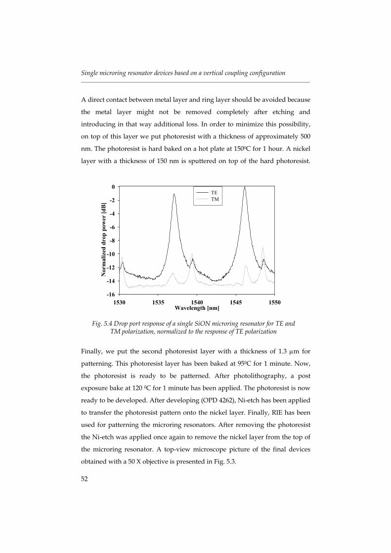
Single microring resonator devices based on a vertical coupling configuration _______________________________________________________________________________________
52
A direct contact between metal layer and ring layer should be avoided because
the metal layer might not be removed completely after etching and
introducing in that way additional loss. In order to minimize this possibility,
on top of this layer we put photoresist with a thickness of approximately 500
nm. The photoresist is hard baked on a hot plate at 1500C for 1 hour. A nickel
layer with a thickness of 150 nm is sputtered on top of the hard photoresist.
Finally, we put the second photoresist layer with a thickness of 1.3 µm for
patterning. This photoresist layer has been baked at 950C for 1 minute. Now,
the photoresist is ready to be patterned. After photolithography, a post
exposure bake at 120 0C for 1 minute has been applied. The photoresist is now
ready to be developed. After developing (OPD 4262), Ni-etch has been applied
to transfer the photoresist pattern onto the nickel layer. Finally, RIE has been
used for patterning the microring resonators. After removing the photoresist
the Ni-etch was applied once again to remove the nickel layer from the top of
the microring resonator. A top-view microscope picture of the final devices
obtained with a 50 X objective is presented in Fig. 5.3.
Fig. 5.4 Drop port response of a single SiON microring resonator for TE and TM polarization, normalized to the response of TE polarization
Wavelength [nm]1530 1535 1540 1545 1550
Nor
mal
ized
dro
p po
wer
[dB
]
-16
-14
-12
-10
-8
-6
-4
-2
0TETM
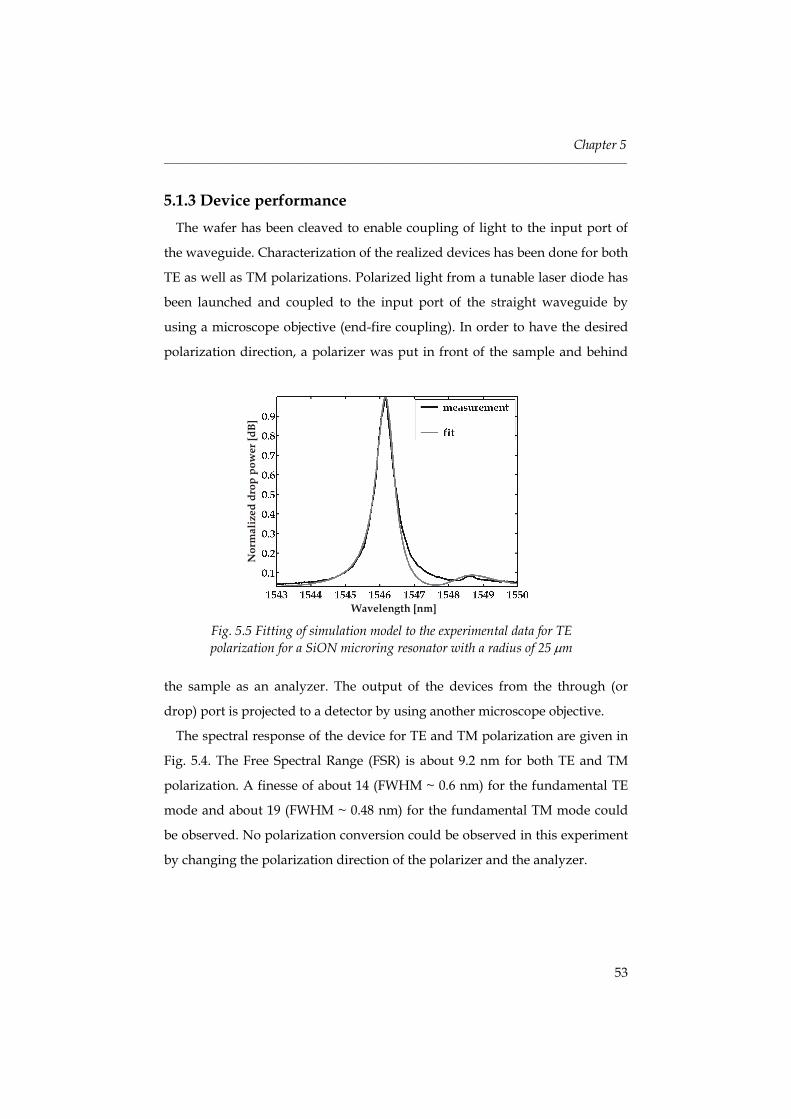
Chapter 5 _______________________________________________________________________________________
53
5.1.3 Device performance The wafer has been cleaved to enable coupling of light to the input port of
the waveguide. Characterization of the realized devices has been done for both
TE as well as TM polarizations. Polarized light from a tunable laser diode has
been launched and coupled to the input port of the straight waveguide by
using a microscope objective (end-fire coupling). In order to have the desired
polarization direction, a polarizer was put in front of the sample and behind
the sample as an analyzer. The output of the devices from the through (or
drop) port is projected to a detector by using another microscope objective.
The spectral response of the device for TE and TM polarization are given in
Fig. 5.4. The Free Spectral Range (FSR) is about 9.2 nm for both TE and TM
polarization. A finesse of about 14 (FWHM ~ 0.6 nm) for the fundamental TE
mode and about 19 (FWHM ~ 0.48 nm) for the fundamental TM mode could
be observed. No polarization conversion could be observed in this experiment
by changing the polarization direction of the polarizer and the analyzer.
Fig. 5.5 Fitting of simulation model to the experimental data for TE polarization for a SiON microring resonator with a radius of 25 µm
Nor
mal
ized
dro
p po
wer
[dB]
Wavelength [nm]
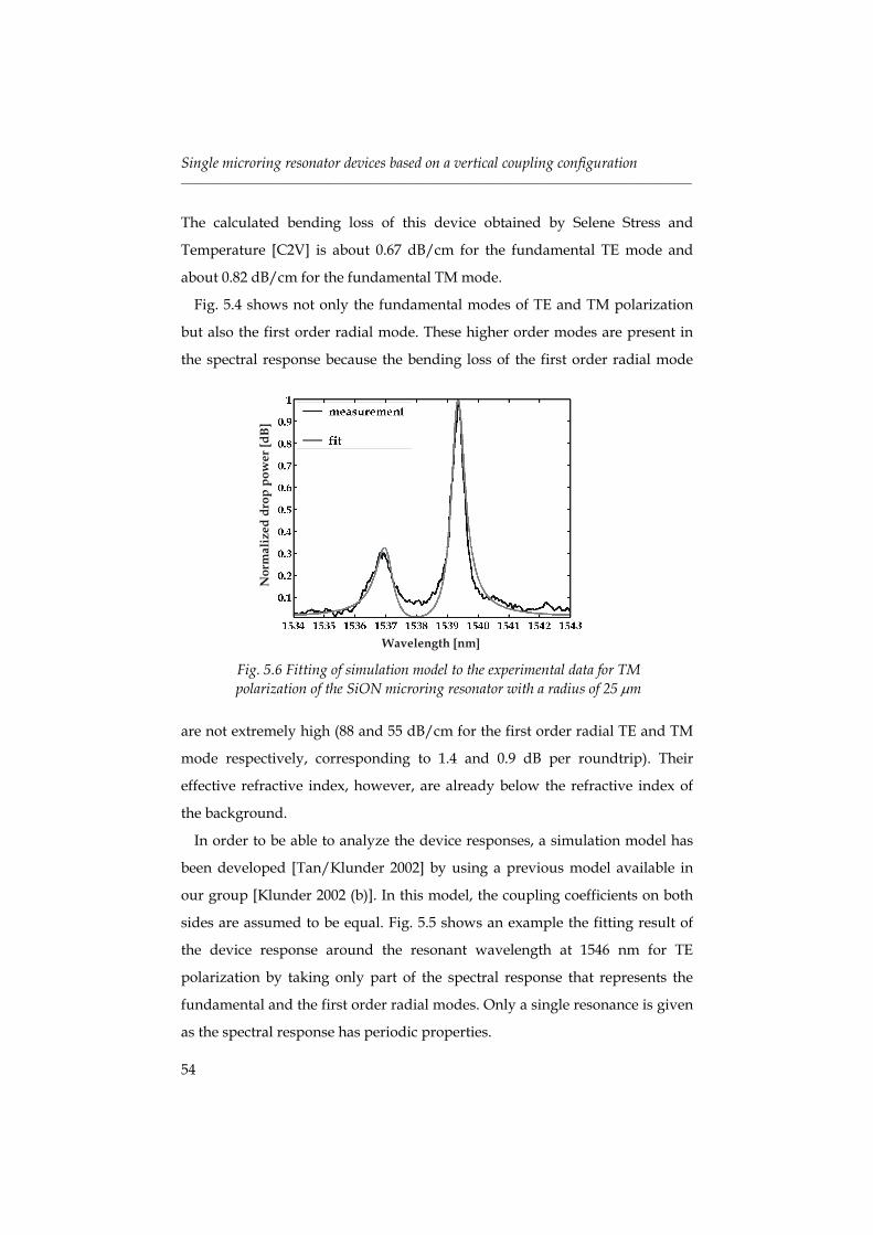
Single microring resonator devices based on a vertical coupling configuration _______________________________________________________________________________________
54
The calculated bending loss of this device obtained by Selene Stress and
Temperature [C2V] is about 0.67 dB/cm for the fundamental TE mode and
about 0.82 dB/cm for the fundamental TM mode.
Fig. 5.4 shows not only the fundamental modes of TE and TM polarization
but also the first order radial mode. These higher order modes are present in
the spectral response because the bending loss of the first order radial mode
are not extremely high (88 and 55 dB/cm for the first order radial TE and TM
mode respectively, corresponding to 1.4 and 0.9 dB per roundtrip). Their
effective refractive index, however, are already below the refractive index of
the background.
In order to be able to analyze the device responses, a simulation model has
been developed [Tan/Klunder 2002] by using a previous model available in
our group [Klunder 2002 (b)]. In this model, the coupling coefficients on both
sides are assumed to be equal. Fig. 5.5 shows an example the fitting result of
the device response around the resonant wavelength at 1546 nm for TE
polarization by taking only part of the spectral response that represents the
fundamental and the first order radial modes. Only a single resonance is given
as the spectral response has periodic properties.
Fig. 5.6 Fitting of simulation model to the experimental data for TM polarization of the SiON microring resonator with a radius of 25 µm
Wavelength [nm]
Nor
mal
ized
dro
p po
wer
[dB]
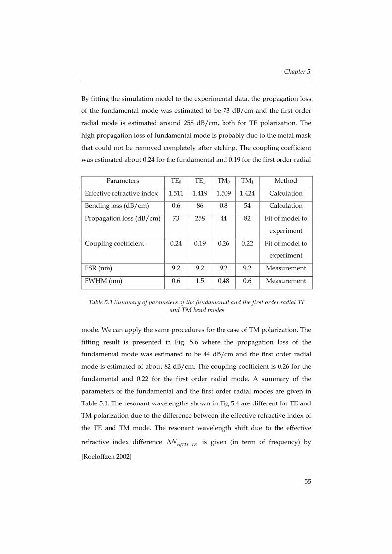
Chapter 5 _______________________________________________________________________________________
55
By fitting the simulation model to the experimental data, the propagation loss
of the fundamental mode was estimated to be 73 dB/cm and the first order
radial mode is estimated around 258 dB/cm, both for TE polarization. The
high propagation loss of fundamental mode is probably due to the metal mask
that could not be removed completely after etching. The coupling coefficient
was estimated about 0.24 for the fundamental and 0.19 for the first order radial
Parameters TE0 TE1 TM0 TM1 Method
Effective refractive index 1.511 1.419 1.509 1.424 Calculation
Bending loss (dB/cm) 0.6 86 0.8 54 Calculation
Propagation loss (dB/cm) 73 258 44 82 Fit of model to
experiment
Coupling coefficient 0.24 0.19 0.26 0.22 Fit of model to
experiment
FSR (nm) 9.2 9.2 9.2 9.2 Measurement
FWHM (nm) 0.6 1.5 0.48 0.6 Measurement
mode. We can apply the same procedures for the case of TM polarization. The
fitting result is presented in Fig. 5.6 where the propagation loss of the
fundamental mode was estimated to be 44 dB/cm and the first order radial
mode is estimated of about 82 dB/cm. The coupling coefficient is 0.26 for the
fundamental and 0.22 for the first order radial mode. A summary of the
parameters of the fundamental and the first order radial modes are given in
Table 5.1. The resonant wavelengths shown in Fig 5.4 are different for TE and
TM polarization due to the difference between the effective refractive index of
the TE and TM mode. The resonant wavelength shift due to the effective
refractive index difference effTM TEN −∆ is given (in term of frequency) by
[Roeloffzen 2002]
Table 5.1 Summary of parameters of the fundamental and the first order radial TE and TM bend modes
Single microring resonator devices based on a vertical coupling configuration _______________________________________________________________________________________
56
effTM TEc c
eff
Nf f
N−∆
∆ = (5.1)
where effN is the effective refractive index and cf is the resonant frequency.
By inspecting Eq. (5.1), the resonant wavelengths shift of the TE and TM
polarization can be estimated. Inserting the effective refractive index
difference of the fundamental TE and TM mode given in Table 5.1 one expects
a shift of 2 nm as also observed experimentally (see Fig. 5.4).
These measurements show that it is difficult to use single-ring resonator
devices based on SiON technology for making polarization independent
wavelength filters. A possible solution is described by Klunder et al. [Klunder
2002 (a)] who propose a polarization diversity scheme together with cascading
of several rings.
In order to complete the information of the device, a detail on-chip
characterization based on quantitative image analysis has been done. This
characterization method and its results have been reported in [Tan 2003 (b)]
and are reproduced in the following section.
5.2 Characterization of vertically waveguide coupled microring
resonators by means of quantitative image analysis
In our group, high Finesse microring resonators have been fabricated and
demonstrated [Klunder 2001, Tan 2001 (a)]. They are fabricated based on SiON
technology [Wörhoff 1999] and are laterally coupled to input and output
waveguides. This configuration can be realized relative easily in a one-step
lithographic process. In this way the ring resonator and the straight
waveguides are structured out of the same layer stack. A drawback of this
method, however, is that the resonator and waveguides can not be optimized
independently. Moreover this configuration is relatively sensitive to the
variations of the definition of the gap between the ring resonator and the
adjacent waveguides and therefore requires a very rigorously controlled
photolithographic step.
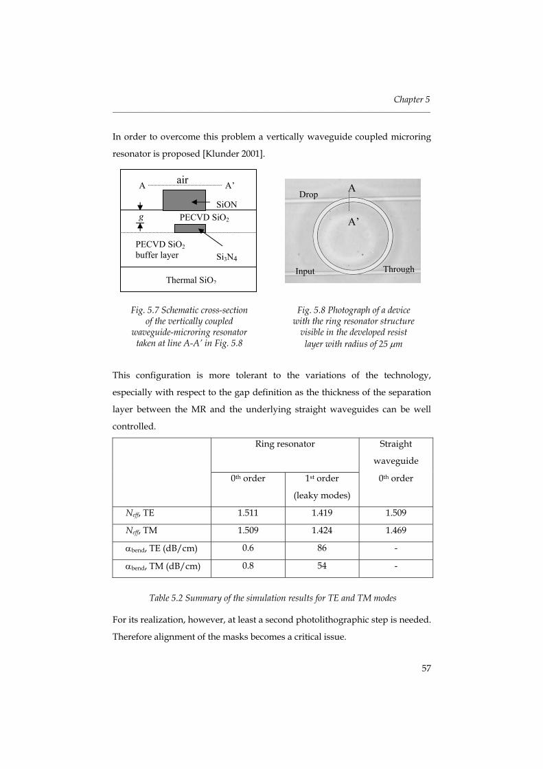
Chapter 5 _______________________________________________________________________________________
57
In order to overcome this problem a vertically waveguide coupled microring
resonator is proposed [Klunder 2001].
This configuration is more tolerant to the variations of the technology,
especially with respect to the gap definition as the thickness of the separation
layer between the MR and the underlying straight waveguides can be well
controlled.
Ring resonator Straight
waveguide
0th order 1st order
(leaky modes)
0th order
Neff, TE 1.511 1.419 1.509
Neff, TM 1.509 1.424 1.469
αbend, TE (dB/cm) 0.6 86 -
αbend, TM (dB/cm) 0.8 54 -
For its realization, however, at least a second photolithographic step is needed.
Therefore alignment of the masks becomes a critical issue.
Fig. 5.8 Photograph of a device with the ring resonator structure
visible in the developed resist layer with radius of 25 µm
A
A’
Input Through
Drop
Fig. 5.7 Schematic cross-section of the vertically coupled
waveguide-microring resonator taken at line A-A’ in Fig. 5.8
air
PECVD SiO2 buffer layer
Thermal SiO2
Si3N4
g PECVD SiO2 SiON
A A’
Table 5.2 Summary of the simulation results for TE and TM modes
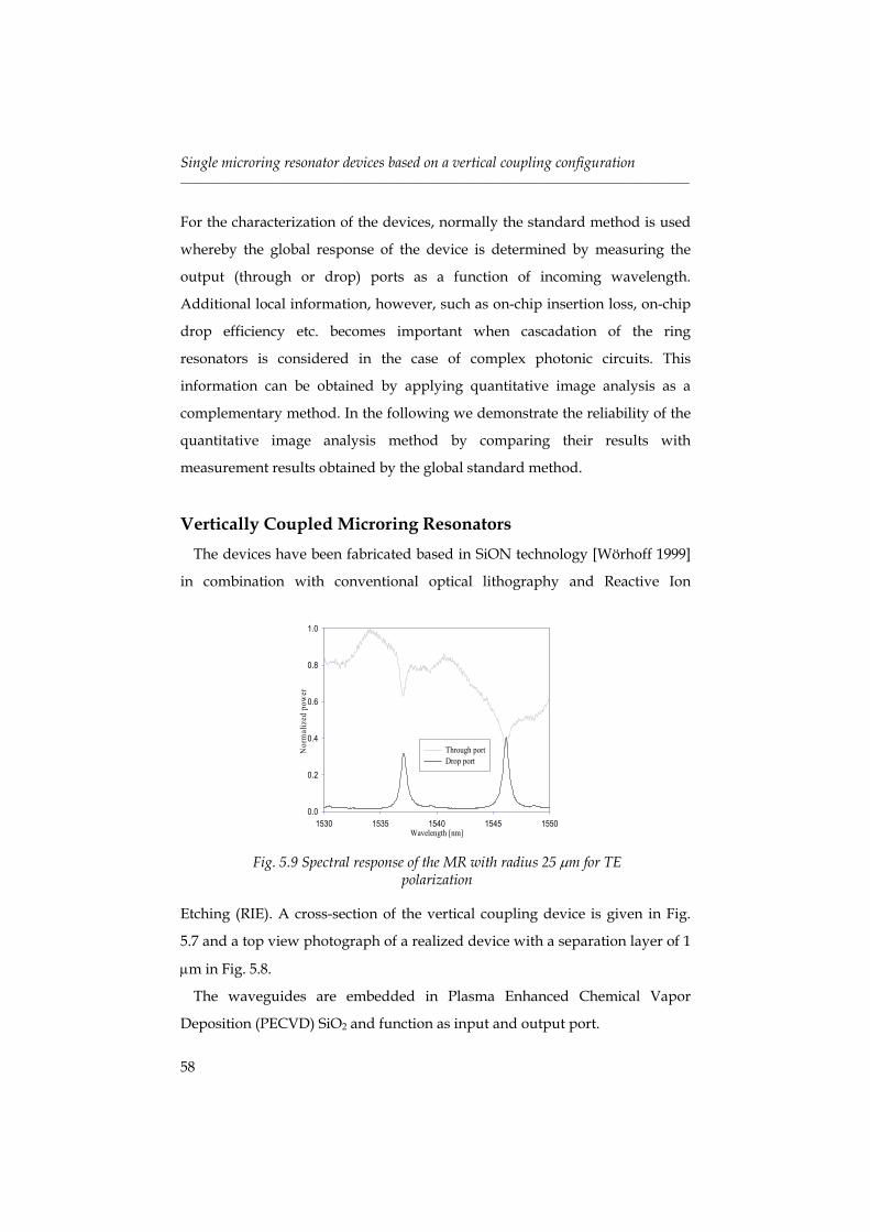
Single microring resonator devices based on a vertical coupling configuration _______________________________________________________________________________________
58
For the characterization of the devices, normally the standard method is used
whereby the global response of the device is determined by measuring the
output (through or drop) ports as a function of incoming wavelength.
Additional local information, however, such as on-chip insertion loss, on-chip
drop efficiency etc. becomes important when cascadation of the ring
resonators is considered in the case of complex photonic circuits. This
information can be obtained by applying quantitative image analysis as a
complementary method. In the following we demonstrate the reliability of the
quantitative image analysis method by comparing their results with
measurement results obtained by the global standard method.
Vertically Coupled Microring Resonators The devices have been fabricated based in SiON technology [Wörhoff 1999]
in combination with conventional optical lithography and Reactive Ion
Etching (RIE). A cross-section of the vertical coupling device is given in Fig.
5.7 and a top view photograph of a realized device with a separation layer of 1
µm in Fig. 5.8.
The waveguides are embedded in Plasma Enhanced Chemical Vapor
Deposition (PECVD) SiO2 and function as input and output port.
Wavelength [nm]1530 1535 1540 1545 1550
Nor
mal
ized
pow
er
0.0
0.2
0.4
0.6
0.8
1.0
Through portDrop port
Fig. 5.9 Spectral response of the MR with radius 25 µm for TE polarization
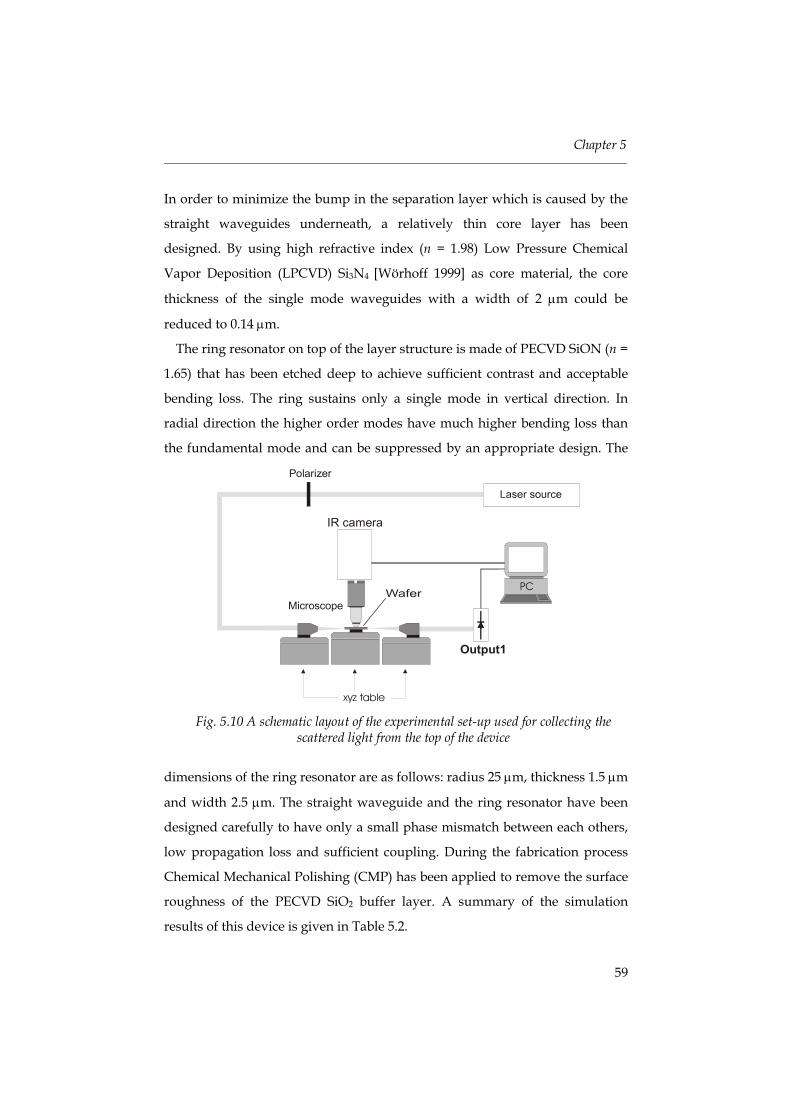
Chapter 5 _______________________________________________________________________________________
59
In order to minimize the bump in the separation layer which is caused by the
straight waveguides underneath, a relatively thin core layer has been
designed. By using high refractive index (n = 1.98) Low Pressure Chemical
Vapor Deposition (LPCVD) Si3N4 [Wörhoff 1999] as core material, the core
thickness of the single mode waveguides with a width of 2 µm could be
reduced to 0.14 µm.
The ring resonator on top of the layer structure is made of PECVD SiON (n =
1.65) that has been etched deep to achieve sufficient contrast and acceptable
bending loss. The ring sustains only a single mode in vertical direction. In
radial direction the higher order modes have much higher bending loss than
the fundamental mode and can be suppressed by an appropriate design. The
dimensions of the ring resonator are as follows: radius 25 µm, thickness 1.5 µm
and width 2.5 µm. The straight waveguide and the ring resonator have been
designed carefully to have only a small phase mismatch between each others,
low propagation loss and sufficient coupling. During the fabrication process
Chemical Mechanical Polishing (CMP) has been applied to remove the surface
roughness of the PECVD SiO2 buffer layer. A summary of the simulation
results of this device is given in Table 5.2.
Fig. 5.10 A schematic layout of the experimental set-up used for collecting the scattered light from the top of the device
Microscope
xyz table
Output1
Polarizer
PC
IR camera
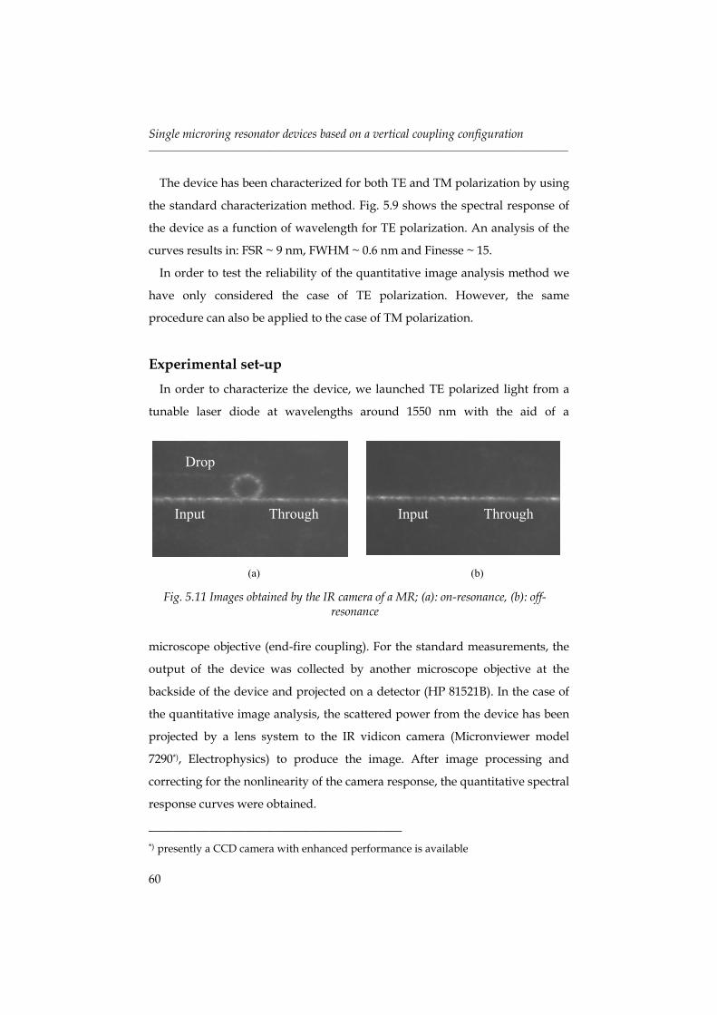
Single microring resonator devices based on a vertical coupling configuration _______________________________________________________________________________________
60
The device has been characterized for both TE and TM polarization by using
the standard characterization method. Fig. 5.9 shows the spectral response of
the device as a function of wavelength for TE polarization. An analysis of the
curves results in: FSR ~ 9 nm, FWHM ~ 0.6 nm and Finesse ~ 15.
In order to test the reliability of the quantitative image analysis method we
have only considered the case of TE polarization. However, the same
procedure can also be applied to the case of TM polarization.
Experimental set-up In order to characterize the device, we launched TE polarized light from a
tunable laser diode at wavelengths around 1550 nm with the aid of a
microscope objective (end-fire coupling). For the standard measurements, the
output of the device was collected by another microscope objective at the
backside of the device and projected on a detector (HP 81521B). In the case of
the quantitative image analysis, the scattered power from the device has been
projected by a lens system to the IR vidicon camera (Micronviewer model
7290*), Electrophysics) to produce the image. After image processing and
correcting for the nonlinearity of the camera response, the quantitative spectral
response curves were obtained.
__________________________________________ *) presently a CCD camera with enhanced performance is available
Throug
(a) (b)
Fig. 5.11 Images obtained by the IR camera of a MR; (a): on-resonance, (b): off-resonance
Drop
Input Through Input Through
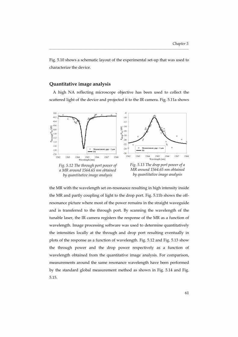
Chapter 5 _______________________________________________________________________________________
61
Fig. 5.10 shows a schematic layout of the experimental set-up that was used to
characterize the device.
Quantitative image analysis A high NA reflecting microscope objective has been used to collect the
scattered light of the device and projected it to the IR camera. Fig. 5.11a shows
the MR with the wavelength set on-resonance resulting in high intensity inside
the MR and partly coupling of light to the drop port. Fig. 5.11b shows the off-
resonance picture where most of the power remains in the straight waveguide
and is transferred to the through port. By scanning the wavelength of the
tunable laser, the IR camera registers the response of the MR as a function of
wavelength. Image processing software was used to determine quantitatively
the intensities locally at the through and drop port resulting eventually in
plots of the response as a function of wavelength. Fig. 5.12 and Fig. 5.13 show
the through power and the drop power respectively as a function of
wavelength obtained from the quantitative image analysis. For comparison,
measurements around the same resonance wavelength have been performed
by the standard global measurement method as shown in Fig. 5.14 and Fig.
5.15.
Fig. 5.12 The through port power of a MR around 1564.65 nm obtained
by quantitative image analysis
Wavelength [nm]1562 1563 1564 1565 1566 1567 1568
P thr
ough
/Pin
[dB
]
-2.0
-1.8
-1.6
-1.4
-1.2
-1.0
-0.8
-0.6
-0.4
-0.2
0.0
Measurement, gap ~ 1 µmFit
Fig. 5.13 The drop port power of a MR around 1564.65 nm obtained
by quantitative image analysis
Wavelength [nm]1562 1563 1564 1565 1566 1567 1568
P dro
p/P i
n [d
B]
-26
-24
-22
-20
-18
-16
-14
-12
-10
-8
Measurement, gap ~ 1 µm Fit
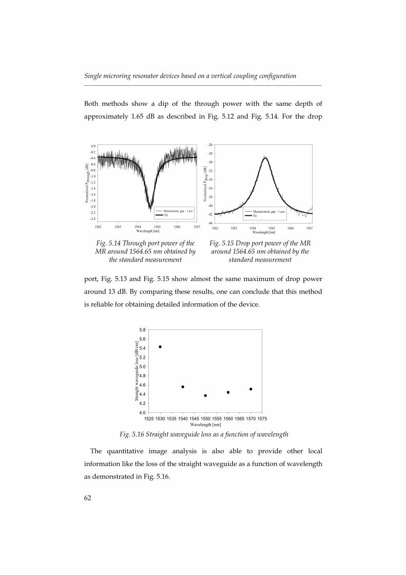
Single microring resonator devices based on a vertical coupling configuration _______________________________________________________________________________________
62
Both methods show a dip of the through power with the same depth of
approximately 1.65 dB as described in Fig. 5.12 and Fig. 5.14. For the drop
port, Fig. 5.13 and Fig. 5.15 show almost the same maximum of drop power
around 13 dB. By comparing these results, one can conclude that this method
is reliable for obtaining detailed information of the device.
The quantitative image analysis is also able to provide other local
information like the loss of the straight waveguide as a function of wavelength
as demonstrated in Fig. 5.16.
Fig. 5.14 Through port power of the MR around 1564.65 nm obtained by
the standard measurement
Wavelength [nm]1562 1563 1564 1565 1566 1567
Nor
mal
ized
Pth
roug
h [d
B]
-2.4-2.2
-2.0
-1.8
-1.6-1.4
-1.2-1.0
-0.8
-0.6
-0.4-0.2
0.0
Measurement, gap ~ 1 µmFit
Fig. 5.15 Drop port power of the MR around 1564.65 nm obtained by the
standard measurement
Wavelength [nm]1562 1563 1564 1565 1566 1567
Nor
mal
ized
Pdr
op [d
B]
-44
-42
-40
-38
-36
-34
-32
-30
-28
-26
Measurement, gap ~ 1 µmFit
Fig. 5.16 Straight waveguide loss as a function of wavelength Wavelength [nm]
1525 1530 1535 1540 1545 1550 1555 1560 1565 1570 1575
Stra
ight
wav
egui
de lo
ss [d
B/c
m]
4.0
4.2
4.4
4.6
4.8
5.0
5.2
5.4
5.6
5.8
Chapter 5 _______________________________________________________________________________________
63
The loss was 4.5 dB/cm around the resonance at 1564.65 nm. The enhanced
loss around 1530 nm is due to N-H overtone vibration, observed typically for
as deposited PECVD SiON [Hussein 2001]. In addition, by making use of Fig.
5.12 and the propagation loss in the straight waveguide we can determine the
on-chip insertion loss of the device at off-resonance to be less than 0.1 dB.
Analysis of the power in the drop port results in an on-chip drop efficiency,
(Pdrop/Pin) of about 10 %.
Single microring resonator devices based on a vertical coupling configuration _______________________________________________________________________________________
64
5.3 Silicon Nitride based microring resonator devices In the foregoing we described in detail the design, fabrication and
characterization of SiON based single microresonators in the vertical coupling
arrangement. In this section, the potential of Si3N4 based ring resonators is
studied as part of a complex configuration foreseen within the NAIS project.
In the following we give results obtained with single microring devices. In Ch.
6 we present our results with more complex devices based on multiple
microrings.
The devices described in the following make use of LPCVD Si3N4 for the
core of the straight waveguide as well as of the microring resonators. The
effective refractive index difference between the straight waveguides and the
microring resonators again has been optimized to be as low as possible to have
a sufficiently low phasemismatch as discussed previously.
5.3.1 Design considerations For the application in the NAIS project, the straight waveguide is designed
to support only a single TE mode in vertical and horizontal direction. It
appears that the design described in Sec. 5.1.1 is a good choice also for the
present case. The microring resonator has been designed to work only for TE polarization.
Applying similar considerations as given in Sec. 5.1.1 we end up with a ring
resonator with a radius of 25 µm, a width of 2.5 µm and a thickness of 300 nm.
The details of the fabrication process for complete devices are given in the
following section.
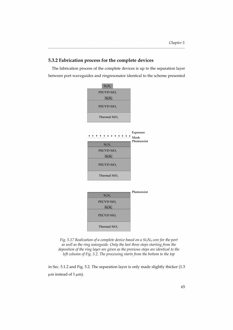
Chapter 5 _______________________________________________________________________________________
65
5.3.2 Fabrication process for the complete devices The fabrication process of the complete devices is up to the separation layer
between port waveguides and ringresonator identical to the scheme presented
in Sec. 5.1.2 and Fig. 5.2. The separation layer is only made slightly thicker (1.3
µm instead of 1 µm).
Fig. 5.17 Realization of a complete device based on a Si3N4 core for the port as well as the ring waveguide. Only the last three steps starting from the
deposition of the ring layer are given as the previous steps are identical to the left column of Fig. 5.2. The processing starts from the bottom to the top
MaskExposure
Si N3 4
PECVD SiO2
Si N3 4
Thermal SiO2
PECVD SiO2
PECVD SiO2
Si N3 4
Thermal SiO2
PECVD SiO2
Photoresist
Si N3 4
PECVD SiO2
Si N3 4
Thermal SiO2
PECVD SiO2
PECVD SiO2
Si N3 4
Thermal SiO2
PECVD SiO2
Si N3 4
PECVD SiO2
Si N3 4
Thermal SiO2
PECVD SiO2
PECVD SiO2
Si N3 4
Thermal SiO2
PECVD SiO2
Photoresist
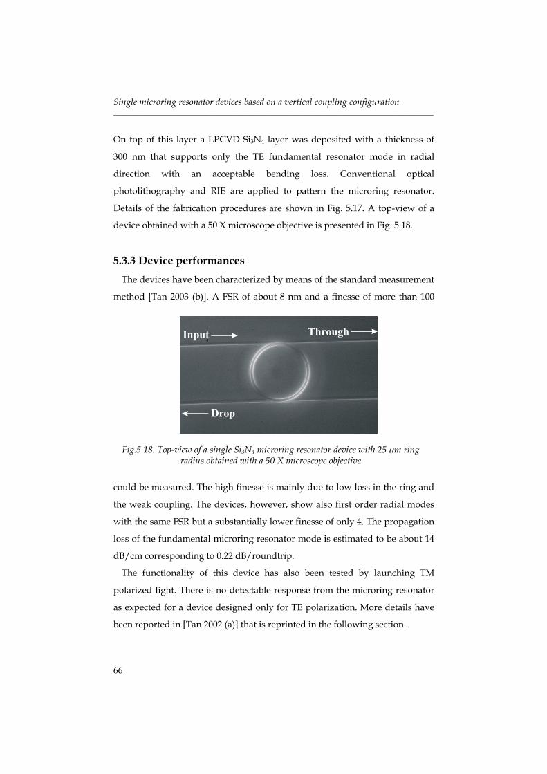
Single microring resonator devices based on a vertical coupling configuration _______________________________________________________________________________________
66
On top of this layer a LPCVD Si3N4 layer was deposited with a thickness of
300 nm that supports only the TE fundamental resonator mode in radial
direction with an acceptable bending loss. Conventional optical
photolithography and RIE are applied to pattern the microring resonator.
Details of the fabrication procedures are shown in Fig. 5.17. A top-view of a
device obtained with a 50 X microscope objective is presented in Fig. 5.18.
5.3.3 Device performances The devices have been characterized by means of the standard measurement
method [Tan 2003 (b)]. A FSR of about 8 nm and a finesse of more than 100
could be measured. The high finesse is mainly due to low loss in the ring and
the weak coupling. The devices, however, show also first order radial modes
with the same FSR but a substantially lower finesse of only 4. The propagation
loss of the fundamental microring resonator mode is estimated to be about 14
dB/cm corresponding to 0.22 dB/roundtrip.
The functionality of this device has also been tested by launching TM
polarized light. There is no detectable response from the microring resonator
as expected for a device designed only for TE polarization. More details have
been reported in [Tan 2002 (a)] that is reprinted in the following section.
Input Through
Drop
Fig.5.18. Top-view of a single Si3N4 microring resonator device with 25 µm ring radius obtained with a 50 X microscope objective
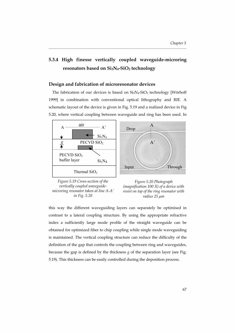
Chapter 5 _______________________________________________________________________________________
67
5.3.4 High finesse vertically coupled waveguide-microring
resonators based on Si3N4-SiO2 technology
Design and fabrication of microresonator devices The fabrication of our devices is based on Si3N4-SiO2 technology [Wörhoff
1999] in combination with conventional optical lithography and RIE. A
schematic layout of the device is given in Fig. 5.19 and a realized device in Fig
5.20, where vertical coupling between waveguide and ring has been used. In
this way the different waveguiding layers can separately be optimised in
contrast to a lateral coupling structure. By using the appropriate refractive
index a sufficiently large mode profile of the straight waveguide can be
obtained for optimized fiber to chip coupling while single mode waveguiding
is maintained. The vertical coupling structure can reduce the difficulty of the
definition of the gap that controls the coupling between ring and waveguides,
because the gap is defined by the thickness g of the separation layer (see Fig.
5.19). This thickness can be easily controlled during the deposition process.
A
A’
Input Through
Drop
Figure 5.20 Photograph (magnification 100 X) of a device with resist on top of the ring resonator with
radius 25 µm
Figure 5.19 Cross-section of the vertically coupled waveguide-
microring resonator taken at line A-A’ in Fig. 5.20
air
PECVD SiO2 buffer layer
Thermal SiO2
Si3N4
g PECVD SiO2 Si3N4
A A’
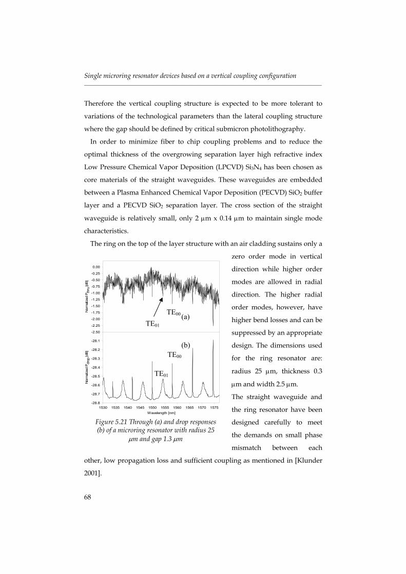
Single microring resonator devices based on a vertical coupling configuration _______________________________________________________________________________________
68
Therefore the vertical coupling structure is expected to be more tolerant to
variations of the technological parameters than the lateral coupling structure
where the gap should be defined by critical submicron photolithography.
In order to minimize fiber to chip coupling problems and to reduce the
optimal thickness of the overgrowing separation layer high refractive index
Low Pressure Chemical Vapor Deposition (LPCVD) Si3N4 has been chosen as
core materials of the straight waveguides. These waveguides are embedded
between a Plasma Enhanced Chemical Vapor Deposition (PECVD) SiO2 buffer
layer and a PECVD SiO2 separation layer. The cross section of the straight
waveguide is relatively small, only 2 µm x 0.14 µm to maintain single mode
characteristics.
The ring on the top of the layer structure with an air cladding sustains only a
zero order mode in vertical
direction while higher order
modes are allowed in radial
direction. The higher radial
order modes, however, have
higher bend losses and can be
suppressed by an appropriate
design. The dimensions used
for the ring resonator are:
radius 25 µm, thickness 0.3
µm and width 2.5 µm.
The straight waveguide and
the ring resonator have been
designed carefully to meet
the demands on small phase
mismatch between each
other, low propagation loss and sufficient coupling as mentioned in [Klunder
2001].
Figure 5.21 Through (a) and drop responses (b) of a microring resonator with radius 25
µm and gap 1.3 µm
Nor
mal
ized
Pth
ru [d
B]
-2.50
-2.25
-2.00
-1.75
-1.50
-1.25
-1.00
-0.75
-0.50
-0.25
0.00
Wavelength [nm]1530 1535 1540 1545 1550 1555 1560 1565 1570 1575
Nor
mal
ized
Pdr
op [d
B]
-28.8
-28.7
-28.6
-28.5
-28.4
-28.3
-28.2
-28.1
TE00
TE01
TE00
TE01 (a)
(b)
Chapter 5 _______________________________________________________________________________________
69
During the fabrication process Chemical Mechanical Polishing (CMP) has been
applied to remove the surface roughness of the PECVD SiO2 buffer layer and
planarization of the PECVD SiO2 separation layer. As an example we show in
Fig. 5.20 the photograph of one of our devices with a separation layer of 1.3
µm. The effective index of this ring for the fundamental TE mode neff ~ 1.53
results in a calculated bend loss of circa 2.5 dB/cm; for the straight waveguide
one has neff ~ 1.51.
Results and discussions In order to characterize the device, we launched TE polarized light of a
tunable laser diode to the input port of the straight waveguide and measured
the spectral response in the 1550 nm region. Fig. 5.21 shows the responses of
the devices at the 'Through' (Fig. 5.21a) and 'Drop' (Fig. 5.21b) ports.
Analysis of the spectral response by using a detailed fitting procedure as
described in [Klunder 2000], gives for the fundamental TE00 mode: Free
Spectral Range (FSR): 8 nm, Finesse: 118 and propagation loss about 14 dB/
cm for a wavelength around 1533 nm. This loss is mainly attributed to the
surface roughness of the ring resonator. In addition we observe also the first
order radial TE01 mode, which has nearly the same FSR of 8 nm but much
lower Finesse (~ 4) due to high bend losses. Fig. 5.21 shows also more
pronounced dips (or peaks) of the fundamental mode for increasing
wavelengths. This indicates strong coupling, which is in agreement with the
results of our fitting procedure. Stronger coupling, however, due to higher
field overlap results in a decreasing Finesse.
Our resonators have been optimised for TE polarization, as it is difficult or
even impossible in practise to obtain polarization independent behaviour.
Only a careful design with simultaneous wavelength trimming [Chu 1999 (a)]
could avoid this drawback. Another approach is to employ a polarization-
diversity scheme [Klunder 2002 (a)].
Single microring resonator devices based on a vertical coupling configuration _______________________________________________________________________________________
70
Conclusions
Microring resonator devices with the vertical coupling configuration have
been realized by conventional optical photolithography in SiON and Si3N4
technology for two different WDM applications.
Moderate high index SiON (n = 1.65) has been chosen as core for the
microring within the BTS project in order to obtain polarization independent
wavelength filters. It appears that it is difficult to obtain with single ring
structures polarization insensitive wavelength filters.
As in the NAIS project a polarization diversity scheme is considered, the
resonator devices can be optimized for a single polarization (TE). Therefore
high index Si3N4 has been chosen as core material. Microrings with a finesse of
more than 100 have been realized and demonstrated. Also in the case of
vertical coupling the high finesse is due to the weak coupling between the port
and ring waveguides and the relatively low propagation loss of the resonators.
Chapter 6 _______________________________________________________________________________________
71
Chapter 6
Cascaded multiple microring resonators as optical
bandpass filters
In the previous chapters, devices consisting of single microring resonators
have been discussed. A lot of effort has been put to gain a deep understanding
of the filter characteristics of the device response and minimizing the
misalignment between the straight waveguides and the microring resonators
in vertical coupling configuration.
Devices consisting of only single microring resonators have already been
shown to exhibit a promising functionality as optical filter. The ON-OFF ratio
of the device response can mainly be tuned via the coupling coefficient, κ and
the propagation loss, α [Tan 2003 (c)]. The value of κ is determined by the
thickness of the gap layer, the phasemismatch and the offsets in lateral
direction. The major contributions to the propagation loss, propα are the
radiation loss due to bending, radα , the absorption loss, absα and the
scattering loss, scatα :
prop rad abs scatα α α α= + + (6.1)
A low bending loss can be achieved by using an appropriate geometry of the
microring resonators and a high enough refractive index of the resonator core.
The material loss, which is mainly due to absorption can be minimized by a
special treatment, in the case of SiON by applying an anneal step [Hussein
2001, Wörhoff 1996, Wörhoff 1999]. The scattering loss originates mainly from
surface roughness of the interfaces with high index contrast and can be
reduced by an improved lithography and etch technology and by smoothing
the sidewalls [Ladouceur 1994].
Cascaded multiple microring resonators as optical bandpass filters _______________________________________________________________________________________
72
Even after optimizing the filter characteristics and improving the resonator
losses, single resonator devices do not fulfill all expectations as the Lorentzian
shape of the filter response does not provide sufficient freedom to synthesize
the desired filter response. For a single ring device only a relatively low ON-
OFF ratio, lack of the passband flatness and a narrow stopband rejection [Tan
2003 (e), Yanagase 2002] can be obtained.
Higher order filters based on cascading multiple microring resonators offer
a substantial improvement of the device performance [Chu 1999 (d), Griffel
2000, Grover 2002, Kokubun 2002, Little 2000 (b), Ma 2001, Madsen 1999,
Melloni 2001, Orta 1995, Tan 2003 (e), Yanagase 2002]. Cascading multiple
microring resonators results in additional design freedom so that a box-like
response can be synthesized with broad and flat stop- or passband, large ON-
OFF ratio and sharp roll-off (defined by ∆λ10dB/∆λ3dB).
The higher order filters can be arranged in serial or parallel configurations.
In this chapter, however, only higher order filter in a parallel configuration
will be discussed in detail.
6.1 Design of cascaded multiple microring resonators in the
parallel configuration Like in the case of single resonator devices described in Ch. 5 we designed
single mode port waveguides for TE polarization with a width of 2 µm and a
thickness of 140 nm to be made of LPCVD Si3N4. The microring resonators are
also made from LPCVD Si3N4 and have been designed to be single mode in
vertical direction for TE polarization. Also for the radial direction single mode
behavior could be obtained by reducing the width to 2 µm. The radius of the
microring is 25 µm and the thickness is 300 nm. As discussed before, the
phasemismatch between the straight waveguide and the microring resonator
has been minimized to allow efficient coupling between port waveguides and
ring. In the following the fabrication process is given in some detail.
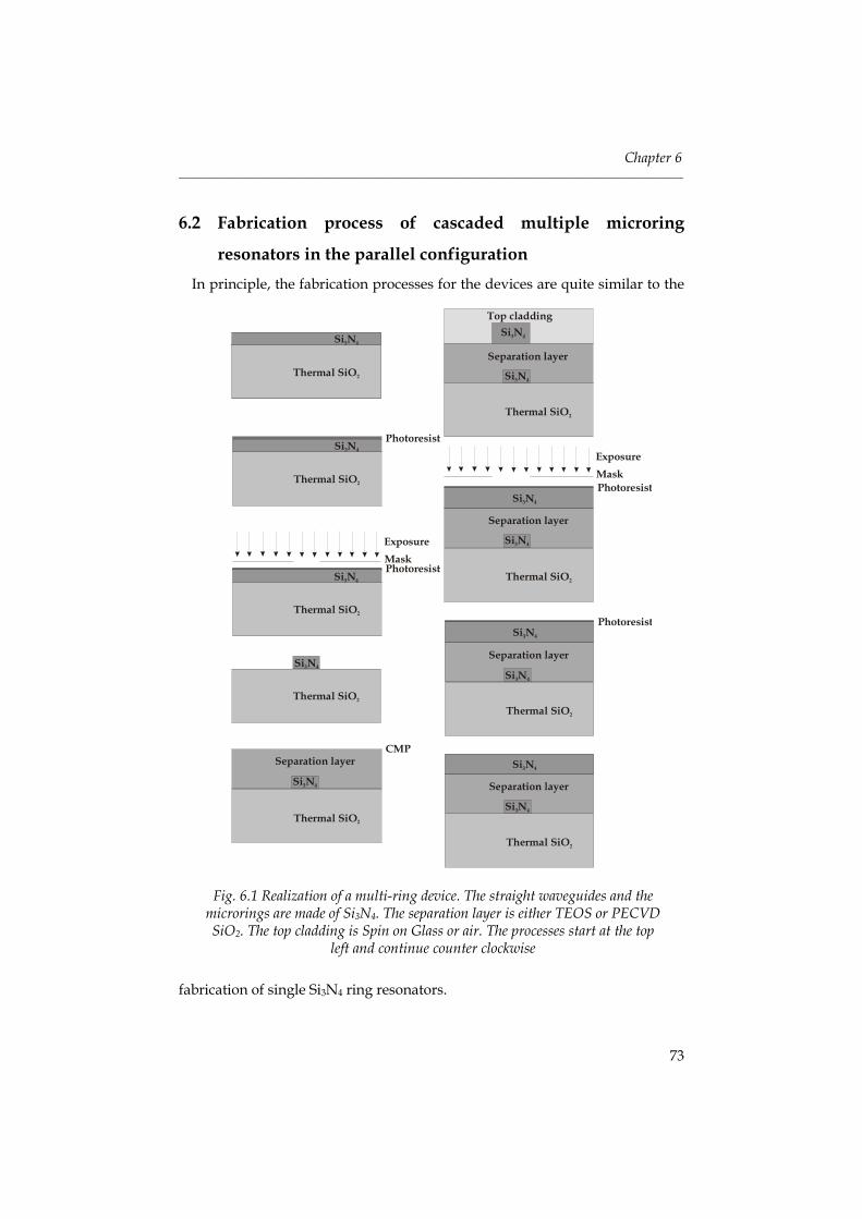
Chapter 6 _______________________________________________________________________________________
73
6.2 Fabrication process of cascaded multiple microring
resonators in the parallel configuration In principle, the fabrication processes for the devices are quite similar to the
fabrication of single Si3N4 ring resonators.
Fig. 6.1 Realization of a multi-ring device. The straight waveguides and the microrings are made of Si3N4. The separation layer is either TEOS or PECVD SiO2. The top cladding is Spin on Glass or air. The processes start at the top
left and continue counter clockwise
Si N3 4
Si N3 4
Thermal SiO2
Photoresist
Thermal SiO2
Si N3 4
Si N3 4
Photoresist
Separation layer
Si N3 4
Thermal SiO2
MaskExposure
Thermal SiO2
Si N3 4
Thermal SiO2
Si N3 4
Thermal SiO2
Si N3 4
Separation layer
Si N3 4
Thermal SiO2
CMP
Thermal SiO2
Photoresist
Thermal SiO2
Si N3 4
MaskExposure
Si N3 4
Photoresist
Separation layer
Si N3 4
Thermal SiO2
Si N3 4
Separation layer
Si N3 4
Thermal SiO2
Top cladding
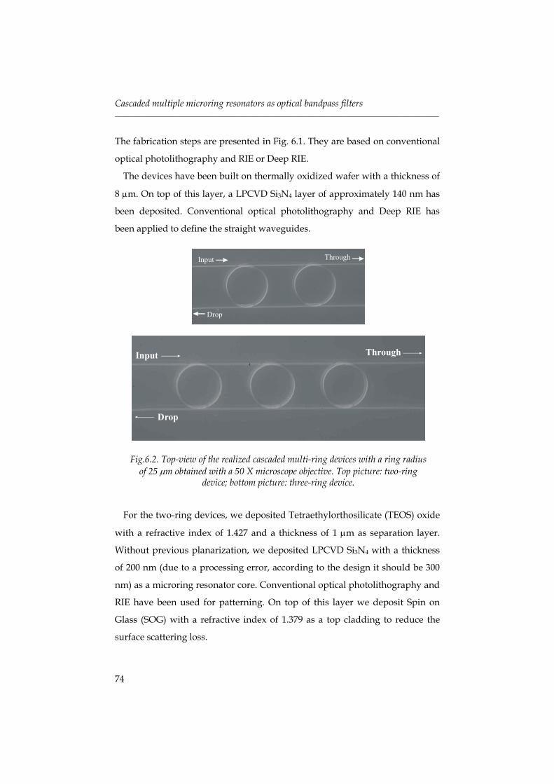
Cascaded multiple microring resonators as optical bandpass filters _______________________________________________________________________________________
74
The fabrication steps are presented in Fig. 6.1. They are based on conventional
optical photolithography and RIE or Deep RIE.
The devices have been built on thermally oxidized wafer with a thickness of
8 µm. On top of this layer, a LPCVD Si3N4 layer of approximately 140 nm has
been deposited. Conventional optical photolithography and Deep RIE has
been applied to define the straight waveguides.
For the two-ring devices, we deposited Tetraethylorthosilicate (TEOS) oxide
with a refractive index of 1.427 and a thickness of 1 µm as separation layer.
Without previous planarization, we deposited LPCVD Si3N4 with a thickness
of 200 nm (due to a processing error, according to the design it should be 300
nm) as a microring resonator core. Conventional optical photolithography and
RIE have been used for patterning. On top of this layer we deposit Spin on
Glass (SOG) with a refractive index of 1.379 as a top cladding to reduce the
surface scattering loss.
Fig.6.2. Top-view of the realized cascaded multi-ring devices with a ring radius of 25 µm obtained with a 50 X microscope objective. Top picture: two-ring
device; bottom picture: three-ring device.
Input Through
Drop
Input Through
Drop
Chapter 6 _______________________________________________________________________________________
75
For the three-ring devices, the separation layer consists of PECVD SiO2 with
a refractive index of 1.46 and a thickness of 1 µm. After deposition,
planarization was done by CMP. A 300 nm thick LPCVD Si3N4 layer has then
been deposited as the microring core layer. Conventional optical
photolithography and RIE have been used for patterning the resonator. No top
cladding layer has been applied. In order to reduce the losses, the device has
been annealed at 1150oC for 4 hours to reduce the hydrogen content [Hussein
2001, Wörhoff 1996, Wörhoff 1999]. Top-view pictures of the final two- and
three-ring devices obtained with a 50 X microscope objective are given in Fig.
6.2.
6.3 Simulation model of cascaded multiple microring
resonators in the parallel configuration For the design of the multi-ring devices and the analysis of the experimental
wavelength response, a simulation model of cascaded multiple microring
resonators in the parallel configuration has been developed. The basic layout
of the devices together with the relevant model parameters are given in Fig.
6.3.
Light is fed into the input port of the straight waveguide and couples in part
to each of the resonators. Each coupler is described by a two-parameters
approach, the coupling coefficient, κmn and the coupling loss, χmn, where m
represents the mth ring and n (1 or 2 for the coupling to the input or drop port
respectively) is related to the coupler position. It is assumed that light
propagates in a unique direction as shown in Fig. 6.3 and that there is no direct
interaction between neighboring rings. The field amplitudes in the straight
waveguide and the microring resonator at each reference plane are given by
amn and cmn respectively. Additional parameters in the model (see also Fig. 6.3)
are the propagation loss inside the ring, αm, the phase shift, φm, the radius of
the ring, Rm and the distance of center to center between two microring
resonators, L.
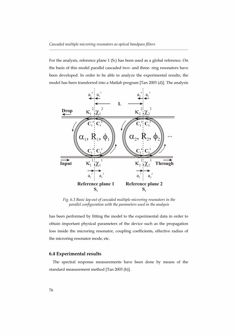
Cascaded multiple microring resonators as optical bandpass filters _______________________________________________________________________________________
76
For the analysis, reference plane 1 (S1) has been used as a global reference. On
the basis of this model parallel cascaded two- and three- ring resonators have
been developed. In order to be able to analyze the experimental results, the
model has been transferred into a Matlab program [Tan 2003 (d)]. The analysis
has been performed by fitting the model to the experimental data in order to
obtain important physical parameters of the device such as the propagation
loss inside the microring resonator, coupling coefficients, effective radius of
the microring resonator mode, etc.
6.4 Experimental results The spectral response measurements have been done by means of the
standard measurement method [Tan 2003 (b)].
Fig. 6.3 Basic lay-out of cascaded multiple microring resonators in the parallel configuration with the parameters used in the analysis
κ χ1 11 1,
κ χ1 12 2,
Input Through
Drop
…
L
a11 a1
2
a14 a1
3
C11
C12C1
3
C14 C2
1
C22C2
3
C24
Reference plane 1S1
Reference plane 2S2
a21 a2
2
a24 a2
3
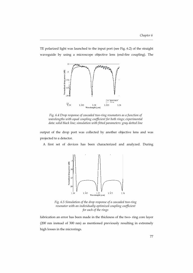
Chapter 6 _______________________________________________________________________________________
77
TE polarized light was launched to the input port (see Fig. 6.2) of the straight
waveguide by using a microscope objective lens (end-fire coupling). The
output of the drop port was collected by another objective lens and was
projected to a detector.
A first set of devices has been characterized and analyzed. During
fabrication an error has been made in the thickness of the two- ring core layer
(200 nm instead of 300 nm) as mentioned previously resulting in extremely
high losses in the microrings.
Fig. 6.5 Simulation of the drop response of a cascaded two-ring resonator with an individually optimized coupling coefficient
for each of the rings
Wavelength [ m]µ
Nor
mal
ized
dro
p po
wer
[dB
]
Fig. 6.4 Drop response of cascaded two-ring resonators as a function of wavelengths with equal coupling coefficient for both rings; experimental data: solid black line; simulation with fitted parameters: gray dotted line
Wavelength [ m]µ
Nor
mal
ized
dro
p po
wer
[dB
]
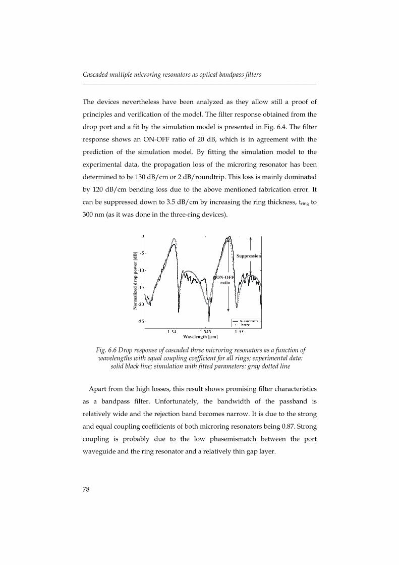
Cascaded multiple microring resonators as optical bandpass filters _______________________________________________________________________________________
78
The devices nevertheless have been analyzed as they allow still a proof of
principles and verification of the model. The filter response obtained from the
drop port and a fit by the simulation model is presented in Fig. 6.4. The filter
response shows an ON-OFF ratio of 20 dB, which is in agreement with the
prediction of the simulation model. By fitting the simulation model to the
experimental data, the propagation loss of the microring resonator has been
determined to be 130 dB/cm or 2 dB/roundtrip. This loss is mainly dominated
by 120 dB/cm bending loss due to the above mentioned fabrication error. It
can be suppressed down to 3.5 dB/cm by increasing the ring thickness, tring to
300 nm (as it was done in the three-ring devices).
Apart from the high losses, this result shows promising filter characteristics
as a bandpass filter. Unfortunately, the bandwidth of the passband is
relatively wide and the rejection band becomes narrow. It is due to the strong
and equal coupling coefficients of both microring resonators being 0.87. Strong
coupling is probably due to the low phasemismatch between the port
waveguide and the ring resonator and a relatively thin gap layer.
Fig. 6.6 Drop response of cascaded three microring resonators as a function of wavelengths with equal coupling coefficient for all rings; experimental data:
solid black line; simulation with fitted parameters: gray dotted line
Wavelength [ m]µ
Nor
mal
ized
dro
p po
wer
[dB
]
Suppression
ON-OFF ratio
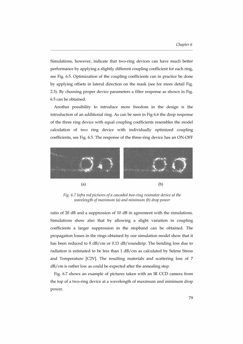
Chapter 6 _______________________________________________________________________________________
79
Simulations, however, indicate that two-ring devices can have much better
performance by applying a slightly different coupling coefficient for each ring,
see Fig. 6.5. Optimization of the coupling coefficients can in practice be done
by applying offsets in lateral direction on the mask (see for more detail Fig.
2.3). By choosing proper device parameters a filter response as shown in Fig.
6.5 can be obtained.
Another possibility to introduce more freedom in the design is the
introduction of an additional ring. As can be seen in Fig 6.6 the drop response
of the three ring device with equal coupling coefficients resembles the model
calculation of two ring device with individually optimized coupling
coefficients, see Fig. 6.5. The response of the three-ring device has an ON-OFF
ratio of 20 dB and a suppression of 10 dB in agreement with the simulations.
Simulations show also that by allowing a slight variation in coupling
coefficients a larger suppression in the stopband can be obtained. The
propagation losses in the rings obtained by our simulation model show that it
has been reduced to 8 dB/cm or 0.13 dB/roundtrip. The bending loss due to
radiation is estimated to be less than 1 dB/cm as calculated by Selene Stress
and Temperature [C2V]. The resulting materials and scattering loss of 7
dB/cm is rather low as could be expected after the annealing step.
Fig. 6.7 shows an example of pictures taken with an IR CCD camera from
the top of a two-ring device at a wavelength of maximum and minimum drop
power.
Fig. 6.7 Infra red pictures of a cascaded two-ring resonator device at the wavelength of maximum (a) and minimum (b) drop power
(a) (b)
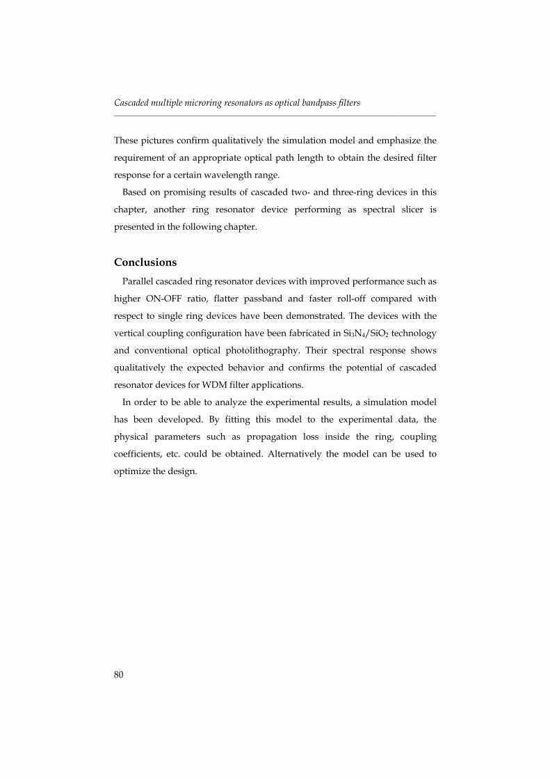
Cascaded multiple microring resonators as optical bandpass filters _______________________________________________________________________________________
80
These pictures confirm qualitatively the simulation model and emphasize the
requirement of an appropriate optical path length to obtain the desired filter
response for a certain wavelength range.
Based on promising results of cascaded two- and three-ring devices in this
chapter, another ring resonator device performing as spectral slicer is
presented in the following chapter.
Conclusions Parallel cascaded ring resonator devices with improved performance such as
higher ON-OFF ratio, flatter passband and faster roll-off compared with
respect to single ring devices have been demonstrated. The devices with the
vertical coupling configuration have been fabricated in Si3N4/SiO2 technology
and conventional optical photolithography. Their spectral response shows
qualitatively the expected behavior and confirms the potential of cascaded
resonator devices for WDM filter applications.
In order to be able to analyze the experimental results, a simulation model
has been developed. By fitting this model to the experimental data, the
physical parameters such as propagation loss inside the ring, coupling
coefficients, etc. could be obtained. Alternatively the model can be used to
optimize the design.
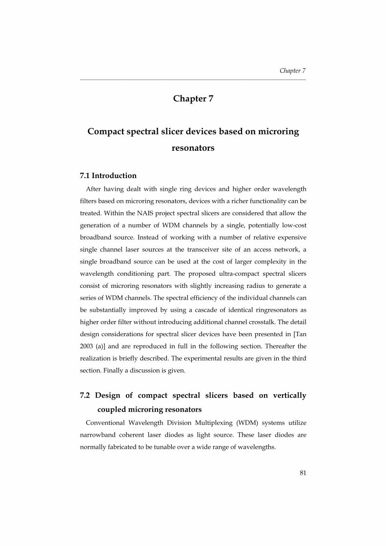
Chapter 7 _______________________________________________________________________________________
81
Chapter 7
Compact spectral slicer devices based on microring
resonators
7.1 Introduction After having dealt with single ring devices and higher order wavelength
filters based on microring resonators, devices with a richer functionality can be
treated. Within the NAIS project spectral slicers are considered that allow the
generation of a number of WDM channels by a single, potentially low-cost
broadband source. Instead of working with a number of relative expensive
single channel laser sources at the transceiver site of an access network, a
single broadband source can be used at the cost of larger complexity in the
wavelength conditioning part. The proposed ultra-compact spectral slicers
consist of microring resonators with slightly increasing radius to generate a
series of WDM channels. The spectral efficiency of the individual channels can
be substantially improved by using a cascade of identical ringresonators as
higher order filter without introducing additional channel crosstalk. The detail
design considerations for spectral slicer devices have been presented in [Tan
2003 (a)] and are reproduced in full in the following section. Thereafter the
realization is briefly described. The experimental results are given in the third
section. Finally a discussion is given.
7.2 Design of compact spectral slicers based on vertically
coupled microring resonators Conventional Wavelength Division Multiplexing (WDM) systems utilize
narrowband coherent laser diodes as light source. These laser diodes are
normally fabricated to be tunable over a wide range of wavelengths.
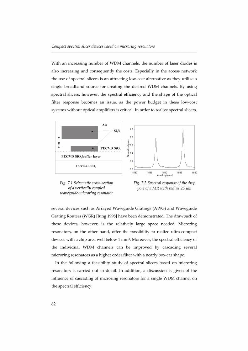
Compact spectral slicer devices based on microring resonators _______________________________________________________________________________________
82
With an increasing number of WDM channels, the number of laser diodes is
also increasing and consequently the costs. Especially in the access network
the use of spectral slicers is an attracting low-cost alternative as they utilize a
single broadband source for creating the desired WDM channels. By using
spectral slicers, however, the spectral efficiency and the shape of the optical
filter response becomes an issue, as the power budget in these low-cost
systems without optical amplifiers is critical. In order to realize spectral slicers,
several devices such as Arrayed Waveguide Gratings (AWG) and Waveguide
Grating Routers (WGR) [Jung 1998] have been demonstrated. The drawback of
these devices, however, is the relatively large space needed. Microring
resonators, on the other hand, offer the possibility to realize ultra-compact
devices with a chip area well below 1 mm2. Moreover, the spectral efficiency of
the individual WDM channels can be improved by cascading several
microring resonators as a higher order filter with a nearly box-car shape.
In the following a feasibility study of spectral slicers based on microring
resonators is carried out in detail. In addition, a discussion is given of the
influence of cascading of microring resonators for a single WDM channel on
the spectral efficiency.
PECVD SiO2
Thermal SiO2
Air
Fig. 7.1 Schematic cross-section of a vertically coupled
waveguide-microring resonator
Wavelength (nm)1530 1535 1540 1545 1550
Nor
mal
ized
pow
er
0.0
0.2
0.4
0.6
0.8
1.0
Fig. 7.2 Spectral response of the drop port of a MR with radius 25 µm
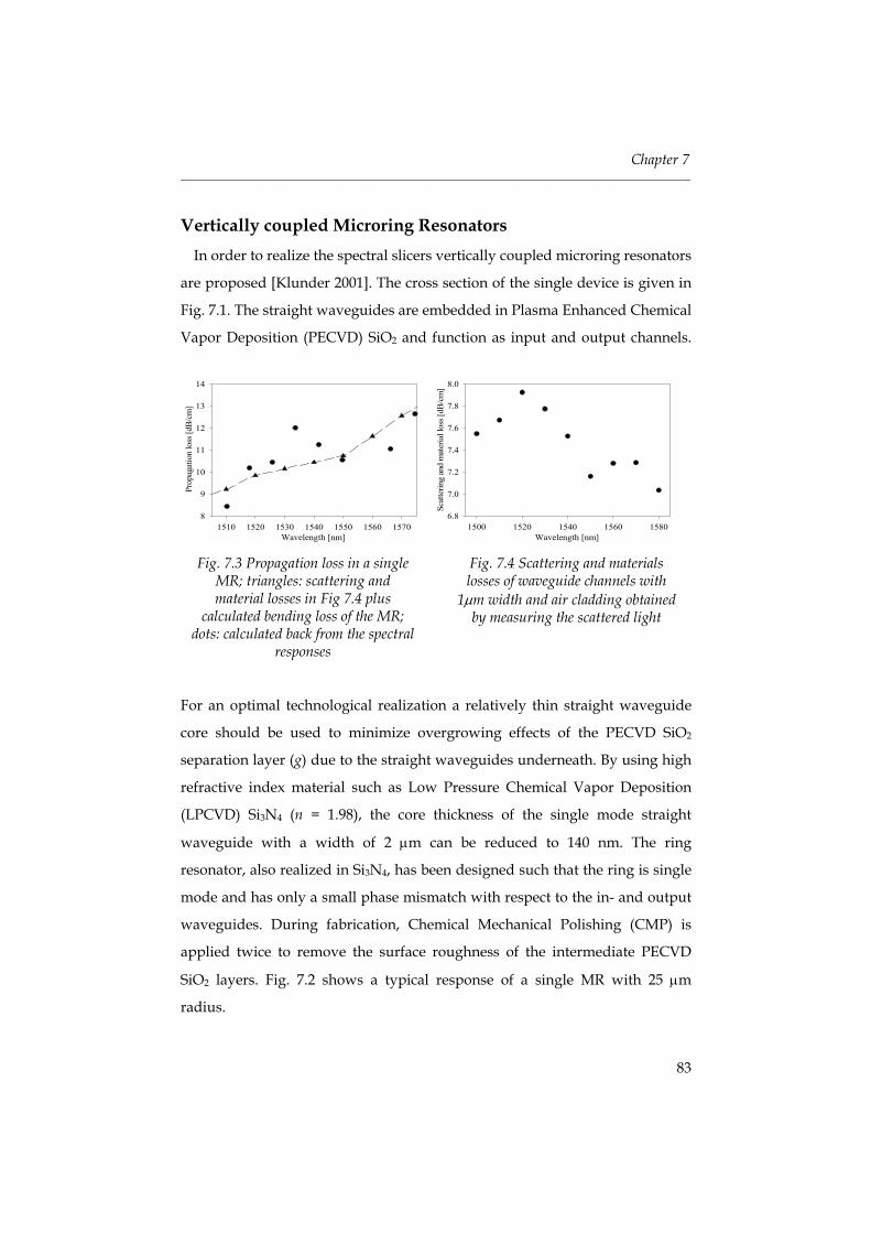
Chapter 7 _______________________________________________________________________________________
83
Vertically coupled Microring Resonators In order to realize the spectral slicers vertically coupled microring resonators
are proposed [Klunder 2001]. The cross section of the single device is given in
Fig. 7.1. The straight waveguides are embedded in Plasma Enhanced Chemical
Vapor Deposition (PECVD) SiO2 and function as input and output channels.
For an optimal technological realization a relatively thin straight waveguide
core should be used to minimize overgrowing effects of the PECVD SiO2
separation layer (g) due to the straight waveguides underneath. By using high
refractive index material such as Low Pressure Chemical Vapor Deposition
(LPCVD) Si3N4 (n = 1.98), the core thickness of the single mode straight
waveguide with a width of 2 µm can be reduced to 140 nm. The ring
resonator, also realized in Si3N4, has been designed such that the ring is single
mode and has only a small phase mismatch with respect to the in- and output
waveguides. During fabrication, Chemical Mechanical Polishing (CMP) is
applied twice to remove the surface roughness of the intermediate PECVD
SiO2 layers. Fig. 7.2 shows a typical response of a single MR with 25 µm
radius.
Fig. 7.3 Propagation loss in a single MR; triangles: scattering and material losses in Fig 7.4 plus
calculated bending loss of the MR; dots: calculated back from the spectral
responses
Wavelength [nm]1510 1520 1530 1540 1550 1560 1570
Prop
agat
ion
loss
[dB
/cm
]
8
9
10
11
12
13
14
Fig. 7.4 Scattering and materials losses of waveguide channels with
1µm width and air cladding obtained by measuring the scattered light
Wavelength [nm]1500 1520 1540 1560 1580
Scat
terin
g an
d m
ater
ial l
oss [
dB/c
m]
6.8
7.0
7.2
7.4
7.6
7.8
8.0
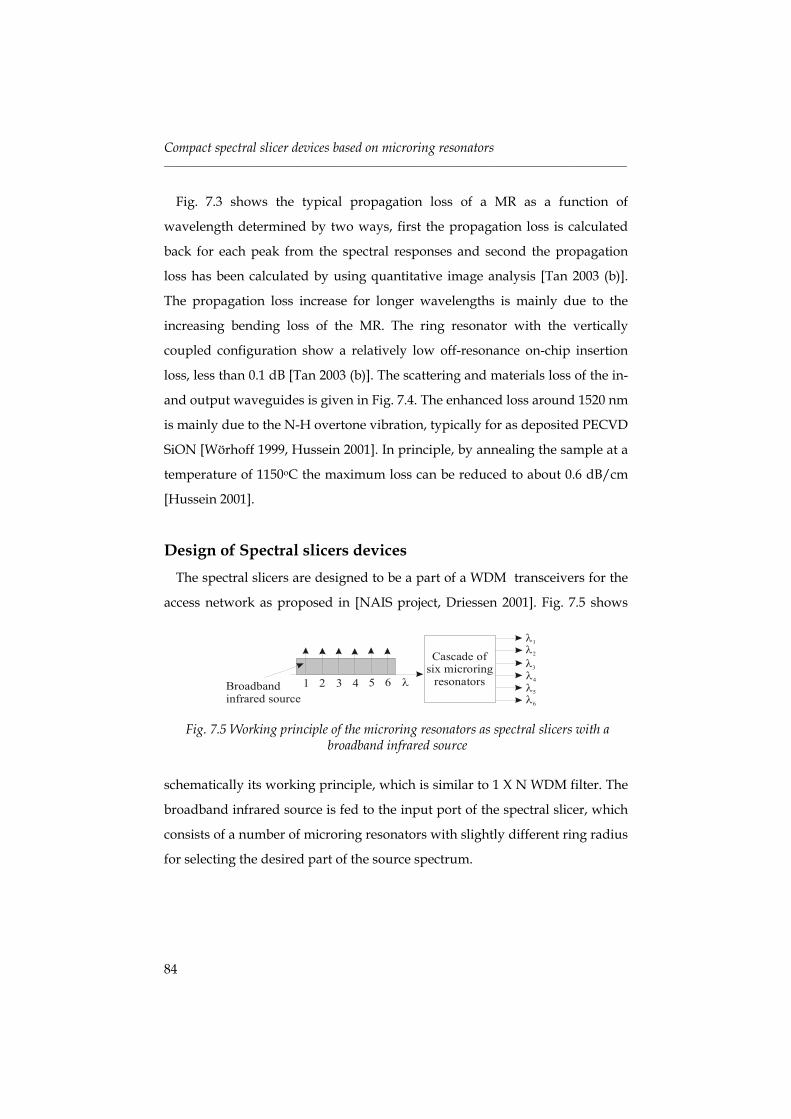
Compact spectral slicer devices based on microring resonators _______________________________________________________________________________________
84
Fig. 7.3 shows the typical propagation loss of a MR as a function of
wavelength determined by two ways, first the propagation loss is calculated
back for each peak from the spectral responses and second the propagation
loss has been calculated by using quantitative image analysis [Tan 2003 (b)].
The propagation loss increase for longer wavelengths is mainly due to the
increasing bending loss of the MR. The ring resonator with the vertically
coupled configuration show a relatively low off-resonance on-chip insertion
loss, less than 0.1 dB [Tan 2003 (b)]. The scattering and materials loss of the in-
and output waveguides is given in Fig. 7.4. The enhanced loss around 1520 nm
is mainly due to the N-H overtone vibration, typically for as deposited PECVD
SiON [Wörhoff 1999, Hussein 2001]. In principle, by annealing the sample at a
temperature of 1150oC the maximum loss can be reduced to about 0.6 dB/cm
[Hussein 2001].
Design of Spectral slicers devices The spectral slicers are designed to be a part of a WDM transceivers for the
access network as proposed in [NAIS project, Driessen 2001]. Fig. 7.5 shows
schematically its working principle, which is similar to 1 X N WDM filter. The
broadband infrared source is fed to the input port of the spectral slicer, which
consists of a number of microring resonators with slightly different ring radius
for selecting the desired part of the source spectrum.
Fig. 7.5 Working principle of the microring resonators as spectral slicers with a broadband infrared source
λ1 2 3 4 5 6
Cascade of six microring
resonators
λ1
λ2
λ3
λ4
λ5
λ6
Broadband infrared source
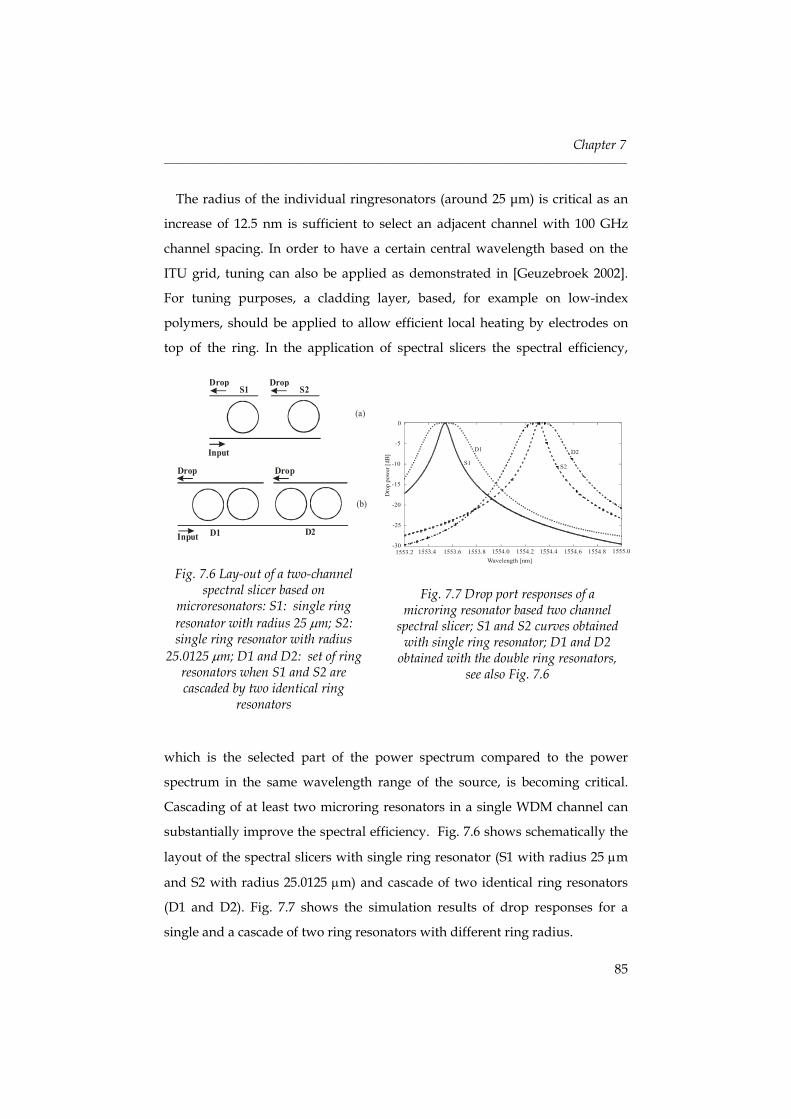
Chapter 7 _______________________________________________________________________________________
85
The radius of the individual ringresonators (around 25 µm) is critical as an
increase of 12.5 nm is sufficient to select an adjacent channel with 100 GHz
channel spacing. In order to have a certain central wavelength based on the
ITU grid, tuning can also be applied as demonstrated in [Geuzebroek 2002].
For tuning purposes, a cladding layer, based, for example on low-index
polymers, should be applied to allow efficient local heating by electrodes on
top of the ring. In the application of spectral slicers the spectral efficiency,
which is the selected part of the power spectrum compared to the power
spectrum in the same wavelength range of the source, is becoming critical.
Cascading of at least two microring resonators in a single WDM channel can
substantially improve the spectral efficiency. Fig. 7.6 shows schematically the
layout of the spectral slicers with single ring resonator (S1 with radius 25 µm
and S2 with radius 25.0125 µm) and cascade of two identical ring resonators
(D1 and D2). Fig. 7.7 shows the simulation results of drop responses for a
single and a cascade of two ring resonators with different ring radius.
Fig. 7.7 Drop port responses of a microring resonator based two channel
spectral slicer; S1 and S2 curves obtained with single ring resonator; D1 and D2
obtained with the double ring resonators, see also Fig. 7.6
k
1553.2 1555.01553.4 1553.6 1553.8 1554.0 1554.2 1554.4 1554.6 1554.8Wavelength [nm]
0
-5
-10
-15
-20
-25
-30
Dro
p po
wer
[dB
]
S1
D1
S2
D2
Fig. 7.6 Lay-out of a two-channel spectral slicer based on
microresonators: S1: single ring resonator with radius 25 µm; S2: single ring resonator with radius
25.0125 µm; D1 and D2: set of ring resonators when S1 and S2 are cascaded by two identical ring
resonators
S1 S2
(a)
D1 D2
(b)
Drop Drop
DropDrop
Input
Input
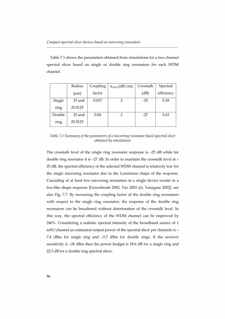
Compact spectral slicer devices based on microring resonators _______________________________________________________________________________________
86
Table 7.1 shows the parameters obtained from simulations for a two channel
spectral slicer based on single or double ring resonators for each WDM
channel.
Radius
(µm)
Coupling
factor
αprop (dB/cm) Crosstalk
(dB)
Spectral
efficiency
Single
ring
25 and
25.0125
0.017 2 -25 0.18
Double
ring
25 and
25.0125
0.04 2 -27 0.43
Table 7.1 Summary of the parameters of a microring resonator based spectral slicer obtained by simulations
The crosstalk level of the single ring resonator response is –25 dB while for
double ring resonator it is –27 dB. In order to maintain the crosstalk level at –
25 dB, the spectral efficiency of the selected WDM channel is relatively low for
the single microring resonator due to the Lorentzian shape of the response.
Cascading of at least two microring resonators in a single device results in a
box-like shape response [Geuzebroek 2002, Tan 2003 (e), Yanagase 2002], see
also Fig. 7.7. By increasing the coupling factor of the double ring resonators
with respect to the single ring resonator, the response of the double ring
resonators can be broadened without deterioration of the crosstalk level. In
this way, the spectral efficiency of the WDM channel can be improved by
240%. Considering a realistic spectral intensity of the broadband source of 1
mW/channel an estimated output power of the spectral slicer per channels is –
7.4 dBm for single ring and –3.7 dBm for double rings. If the receiver
sensitivity is –26 dBm then the power budget is 18.6 dB for a single ring and
22.3 dB for a double ring spectral slicer.
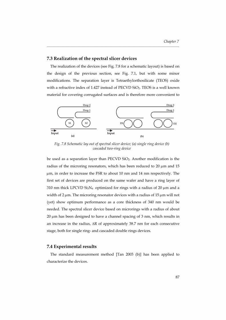
Chapter 7 _______________________________________________________________________________________
87
7.3 Realization of the spectral slicer devices The realization of the devices (see Fig. 7.8 for a schematic layout) is based on
the design of the previous section, see Fig. 7.1, but with some minor
modifications. The separation layer is Tetraethylorthosilicate (TEOS) oxide
with a refractive index of 1.427 instead of PECVD SiO2. TEOS is a well known
material for covering corrugated surfaces and is therefore more convenient to
be used as a separation layer than PECVD SiO2. Another modification is the
radius of the microring resonators, which has been reduced to 20 µm and 15
µm, in order to increase the FSR to about 10 nm and 14 nm respectively. The
first set of devices are produced on the same wafer and have a ring layer of
310 nm thick LPCVD Si3N4 optimized for rings with a radius of 20 µm and a
width of 2 µm. The microring resonator devices with a radius of 15 µm will not
(yet) show optimum performance as a core thickness of 340 nm would be
needed. The spectral slicer device based on microrings with a radius of about
20 µm has been designed to have a channel spacing of 3 nm, which results in
an increase in the radius, ∆R of approximately 38.7 nm for each consecutive
stage, both for single ring- and cascaded double rings devices.
7.4 Experimental results The standard measurement method [Tan 2003 (b)] has been applied to
characterize the devices.
S1 S2
(a)
Drop 2
Drop 1
Input
Drop 2
D1 D2
(b)
Drop 1
Input
Fig. 7.8 Schematic lay out of spectral slicer device; (a) single ring device (b) cascaded two-ring device
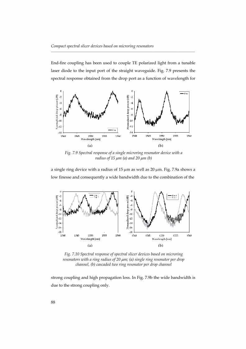
Compact spectral slicer devices based on microring resonators _______________________________________________________________________________________
88
End-fire coupling has been used to couple TE polarized light from a tunable
laser diode to the input port of the straight waveguide. Fig. 7.9 presents the
spectral response obtained from the drop port as a function of wavelength for
a single ring device with a radius of 15 µm as well as 20 µm. Fig. 7.9a shows a
low finesse and consequently a wide bandwidth due to the combination of the
strong coupling and high propagation loss. In Fig. 7.9b the wide bandwidth is
due to the strong coupling only.
(a) (b)
Fig. 7.9 Spectral response of a single microring resonator device with a radius of 15 µm (a) and 20 µm (b)
Fig. 7.10 Spectral response of spectral slicer devices based on microring resonators with a ring radius of 20 µm; (a) single ring resonator per drop
channel, (b) cascaded two ring resonator per drop channel
(a) (b)
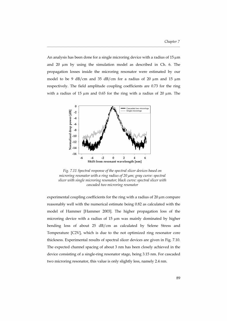
Chapter 7 _______________________________________________________________________________________
89
An analysis has been done for a single microring device with a radius of 15 µm
and 20 µm by using the simulation model as described in Ch. 6. The
propagation losses inside the microring resonator were estimated by our
model to be 9 dB/cm and 35 dB/cm for a radius of 20 µm and 15 µm
respectively. The field amplitude coupling coefficients are 0.73 for the ring
with a radius of 15 µm and 0.65 for the ring with a radius of 20 µm. The
experimental coupling coefficients for the ring with a radius of 20 µm compare
reasonably well with the numerical estimate being 0.82 as calculated with the
model of Hammer [Hammer 2003]. The higher propagation loss of the
microring device with a radius of 15 µm was mainly dominated by higher
bending loss of about 25 dB/cm as calculated by Selene Stress and
Temperature [C2V], which is due to the not optimized ring resonator core
thickness. Experimental results of spectral slicer devices are given in Fig. 7.10.
The expected channel spacing of about 3 nm has been closely achieved in the
device consisting of a single-ring resonator stage, being 3.15 nm. For cascaded
two microring resonator, this value is only slightly less, namely 2.4 nm.
Fig. 7.11 Spectral response of the spectral slicer devices based on microring resonator with a ring radius of 20 µm; gray curve: spectral slicer with single microring resonator; black curve: spectral slicer with
cascaded two microring resonator
Shift from resonant wavelength [nm]-6 -4 -2 0 2 4 6
Nor
mal
ized
dro
p po
wer
[dB]
-16
-14
-12
-10
-8
-6
-4
-2
0Cascaded two microringsSingle microrings
Compact spectral slicer devices based on microring resonators _______________________________________________________________________________________
90
This means that the ring radii are controlled within 8 nm. The crosstalk levels
of the response of both devices are rather high, -9 dB and -7 dB for the single
and the two ring stages respectively as the strong coupling results in
broadening of the bandwidth. When correcting the response of Fig. 7.10b for
the undesired shift in ring radius, the crosstalk is reduced to –11 dB. For a
further reduction in crosstalk the propagation loss inside the microring should
be decreased. In that case a relatively small coupling coefficient can be used
that results in a narrower bandwidth. Moreover, the coupling coefficients can
even more finely tuned to obtain precisely the desired response as was
discussed in Ch. 6.
In order to illustrate the influence of a two-ring stage on the device
performance, the resonant peak of a device with a single microring stage has
been put together with the resonant peak of two ring stage (see Fig. 7.11). The
cascaded two-ring resonator device shows a better rolloff (∆λ-10dB/∆λ-3dB) of
about 1.28 times faster and decreased crosstalk.
The spectral efficiency (η) can be estimated by calculating ∆λ-3dB divided by
a spectral width of a single WDM channel ( w ) or
3dB
wλη −∆
=
The measurement results in Fig. 7.11 are obtained with devices processed on
the same wafer, which means the intended devices have the same coupling
coefficient. In order to be able to compare the spectral efficiency we need
devices with different coupling coefficients as described in the design section
and shown in Table 7.1. However, a faster rolloff and lower crosstalk of the
cascaded device has clearly been demonstrated.
Conclusions
Compact spectral slicer devices based on cascaded microring resonators are
for the first time demonstrated.
Chapter 7 _______________________________________________________________________________________
91
They are realized in Si3N4/SiO2 technology using conventional optical
photolithography and employ the vertical coupling configuration. The devices
with a promising performance can still be improved by tailoring the coupling
coefficients, reducing the propagation loss inside the ring and by cascading
more rings.
The potential of the employed technology has further been explored by
reducing the ring radius and consequently enhancing the FSR. It is shown
experimentally that with the Si3N4/SiO2 technology, a FSR of 10 and 14 nm can
be obtained for rings with 20 and 15 µm respectively. Comparison of resonant
wavelengths of rings designed with identical ring radius reveals that the
employed technology results in variations of the radius about 8 nm, i.e. less
than 0.5 x 10⁻³.

Compact spectral slicer devices based on microring resonators _______________________________________________________________________________________
92
Chapter 8 _______________________________________________________________________________________
93
Chapter 8
Summary and Recommendations
8.1 Summary
This thesis describes work on microring resonator devices based on Silicon
Oxynitride technology carried out in the Dutch BTS and European NAIS
project. In the beginning only single ring devices have been considered in
order to develop the fabrication technology as well as design and
measurement methods and gain a deep understanding of the functional
behavior. Later more complex devices consisting of cascaded multiple
microring resonators in a parallel configuration with a promising functionality
have been realized and demonstrated. In the following a summary and
recommendations for future work will be given.
Chapter 1:
This chapter gives a general overview of optical communication and
the possible role of microring resonator devices as optical filters for
WDM systems. It describes briefly the objective of the BTS and the NAIS
project and ends with a brief outline of this thesis.
Chapter 2:
General concepts of microring resonator devices are given in this
chapter. The working principle of ring resonator devices and the two
basic coupling schemes, lateral and vertical coupling, are described.
Thereafter the performance of cascaded multiple rings in serial and
parallel configuration are discussed.
Summary and Recommendations _______________________________________________________________________________________
94
Finally two characterization methods, the standard method and
quantitative image analysis, are explained in detail.
Chapter 3:
A general route in order to arrive at a realistic design and to realize
eventually demonstrator devices is explained in detail. A lot of
constraints have a great influence on the design activities, for example
the available knowledge, technological facilities and design tools, and
also the objectives and time frame of the project. Several activities
should be carried out such as intermediate characterizations, functional
characterizations followed by system evaluations in order to end up
with the final demonstrator devices.
Chapter 4:
The results obtained with microring resonator devices in the lateral
coupling configuration are reported in this chapter. The Si3N4 based
devices were analyzed in the wavelength range of 1510 to 1580 nm and a
finesse of up to 182 has been achieved. The most critical issue in this
configuration is the gap definition, which is rather difficult to be
obtained with conventional optical photolithography.
Chapter 5:
In this chapter, work on single ring resonator devices based on SiON
and Si3N4 in a vertical coupling configuration are presented. A feasibility
study shows that it is difficult to realize single SiON microring resonator
devices that can perform as polarization independent wavelength filters.
Based on this experience, a polarization diversity scheme is considered
and work has been focused on microring resonators optimized for TE
polarization. Devices have been realized in Si3N4 technology, whereby a
finesse of more than 100 could be demonstrated.
Chapter 8 _______________________________________________________________________________________
95
Chapter 6:
Increasing the complexity of devices by cascading two or three
microring resonators in a parallel configuration a better performance of
the filter response could be obtained. A simulation model is developed
that allows the design and analysis of the multiple ring devices. Devices
have been realized in Si3N4 technology and show a promising
functionality as bandpass filter. Two-ring devices with equal coupling
coefficients exhibit a rather wide passband and narrow stopband, three-
ring devices show increased performance.
Chapter 7:
Another potential application of ring resonator devices, spectral slicers
are presented. Devices based on microresonators with a radius of 20 µm
as well as 15 µm have been designed and realized. A comparison is
made between the performance of devices where each stage is made of
either a single or a double ring configuration. The latter show much
better performance with respect to faster roll-off and lower crosstalk.
Chapter 8:
This chapter presents a summary of the work described in this thesis
and gives also conclusions and recommendations for future work.
8.2 Recommendations
As mentioned in the previous chapters, the performance of the filters is
mainly determined by the coupling coefficients and propagation loss inside
the ring resonator. Therefore simulation tools that can be used to estimate the
coupling coefficients should be available. The propagation loss might be
decreased by applying appropriate fabrication processes.
Summary and Recommendations _______________________________________________________________________________________
96
In the case of the lateral coupling configuration, coupling coefficients can be
estimated by reducing the three-dimensional structure using an effective index
method and calculate the field overlap between the mode in the port
waveguide and the ring as described in [Klunder 2002 (b)]. Estimation of the
coupling coefficients in three-dimensions by a simplified coupled mode theory
[Hammer 2003] and semi-experimental estimations obtained by fitting the
simulation model to the experimental data are in reasonable agreement (see
Sec. 7.4). Fully three-dimensional coupled mode theory, however, is necessary
that enable better comparison between those results and allow improved
optimization of the design to obtain the desired coupling coefficients.
Developing new fabrication approaches might be useful to decrease the
propagation loss inside the ring. With the currently available fabrication
process the absorption and scattering loss is in the order of 6 – 8 dB/cm. An
annealing process would not reduce the propagation losses significantly
because the losses are mainly dominated by the scattering loss. By using a
waferstepper with an overlay accuracy of about 100 nm, alignment problems
between waveguide and ring mask could probably be solved. Also lower
scattering loss could be expected because the roughness on the mask that is
transferred directly to the photoresist in conventional optical
photolithography by using contact printing will be reduced by using a
projection method with size reduction. When the alignment problems have
been solved, the incorporation of precise offsets in horizontal direction on the
mask become useful and the coupling coefficients could be tailored more
efficient to give the desired filter response.
Specific recommendations of some chapters are given in the following:
Chapter 5:
In order to be able to realize polarization independent wavelength filters,
polarization diversity scheme in combination with cascading several rings can
be used (see Klunder 2002 (a)).
Chapter 8 _______________________________________________________________________________________
97
By using this scheme, the devices need to be optimized only for a single
polarization. The validity of this approach, however, should be examined by
experiments.
Chapter 6:
In order to be able to have the desired filter response, the devices might be
tuned e.g. thermo-optically. In the case of parallel cascaded ring devices,
tuning the rings could also change the distance between centre to centre of
nearest neighbor rings causing in that way an undesired filter response.
Additional tuning elements located on the connecting line of the port
waveguides could compensate for this effect.
Chapter 7:
Reducing the ring radius seems to cause problems to the quality of the ring
layer as by increasing the layer thickness, crack can occur and bending of the
wafer. In order to minimize bending of the wafer, growing a layer on both
sides of the wafer might help. By applying these treatments, the layer
properties such as the thickness, refractive index etc. should be carefully
measured as these usually changes.

Summary and Recommendations _______________________________________________________________________________________
98
References _______________________________________________________________________________________
99
References [Abeles 2000] Abeles, J.H., “Resonant enhanced modulator development”, Sarnof Corporation, public release [Albers 1995] Albers, H., Hilderink, L.T.H., Szilagyi, E., Paszti, F., Lambeck, P.V., and Popma, Th.J.A., “Reduction of hydrogen induced losses in PECVD-SiOxNy optical waveguide in the near infrared”, in Proc. IEEE LEOS Annual Meeting 1995, pp. 88-89, 1995 [Absil 2000] Absil, P.P., Hryniewicz, J.V., Little, B.E., Cho, P.S., Wilson, R.A., Joneckis, L.G., and Ho, P.T., “Wavelength conversion in GaAs micro-ring resonators”, Opt. Lett., vol. 25, pp. 554-556, 2000 [Balistreri 2001] Balistreri, M.L.M., Klunder, D.J.W., Blom, F.C., Driessen, A., Korterik, J.P., Kuipers, L., van Hulst, N.F., “Experimental analysis of the whispering gallery modes in a cylindrical optical microresonator”, J. of Opt. Soc. Am. B, vol. 18, pp. 465-471, 2001 [Bertolotti 2004] Bertolotti, M., Driessen, A. and Michelotti, F. (editors), “Micro resonators as Building blocks for VLSI Photonics”, in Proc. International School of Quantum Electronics, Enrice-Sicily, October 2003, AIP 2004. [Blom 1996] Blom, F.C., Hoekstra, H.J.W.M., Driessen, A. and Popma, Th. J.A., “A new integrated all-optical switch based on a micro-cavity”, in Proc. CLEO-Europe 1996, pp. 20-20, Hamburg, 1996 [Blom 1997] Blom, F.C., van Dijk, D.R., Hoekstra, H.J.W.M., Driessen, A. and Popma, Th. J.A., “Experimental study of integrated optics microcavity resonators: towards and all-optical switching device”, Appl. Phys. Lett., vol. 71, pp. 747-749, 1997 [Blom 1998] Blom, F.C., Linear and non-linear optical properties of cylindrical micro-resonators from materials to device realization, Ph.D thesis 1998, University of Twente, The Netherlands
References _______________________________________________________________________________________
100
[Blom 1999] Blom, F.C., Kelderman, H., Hoekstra, H.J.W.M., Driessen, A., Popma, Th. J. A., Chu, S.T. and Little, B.E., “A single channel dropping filter based on a cylindrical micro-resonator”, Opt. Comm., vol. 167, pp. 77-82, 1999 [BTS project] Project description [C2V] Selene Stress & Temperature and Prometheus DV, commercial product of C2V, Colosseum 20, 7521 PT Enschede, The Netherlands [Chin 1999] Chin, M.K., Youtsey, C., Zhao, W., Pierson, T., Ren, Z., Wu, S.L., Wang, L., Zhao, Y.G., and Ho, S.T., “GaAs microcavity channel-dropping filter based on race-track resonator”, IEEE Photon. Technol. Lett., vol. 11, pp. 1620-1622, 1999 [Chu 1999 (a)] Chu, S.T., Pan, W., Sato, S., Kaneko, T., Little, B.E., Kokubun, Y., “Wavelength trimming of a microring resonator filter by means of a UV sensitive polymer overlay”, IEEE Photon. Technol. Lett., vol. 11, pp. 688-690, 1999 [Chu 1999 (b)] Chu, S.T., Little, B.E., Pan, W., Kaneko, T., Sato, S., and Kokubun, Y., “An eight-channel add-drop filter using vertically coupled microring resonators over as cross grid”, IEEE Photon. Technol. Lett., vol. 11, pp. 691-693, 1999 [Chu 1999 (c)] Chu, S.T., Pan, W., Suzuki, S., Little, B.E., Sato, S., and Kokubun, Y., “Temperature insensitive vertically coupled microring resonator add/drop filters by means of a polymer overlay”, IEEE Photon. Technol. Lett., vol. 11, pp. 1138-1140, 1999 [Chu 1999 (d)] Chu, S.T., Little, B.E., Pan, W., Kaneko, T., Kokubun, Y., “Second-order filter response from parallel coupled glass microring resonators”, IEEE. Photon. Technol. Lett., vol. 11, pp. 1426-1428, 1999 [Dapkus 2000] Dapkus, D., O’Brien, J., Low voltage modulator based on semiconductor microresonators, RFLICS kickoff meeting, public release
References _______________________________________________________________________________________
101
[Driessen 2001] Driessen, A., Geuzebroek, D.H., Klunder, D.J.W. and Tan, F.S., “Analysis of a microring resonator based ultra-compact transceiver for the access network”, in Proc. LEOS Benelux Chapter 2001, pp. 25–28, 2001 [Driessen 2003] Driessen, A, Geuzebroek, D.H., Hoekstra, H.J.W.M.,
Kelderman, H., Klein, E.J., Klunder, D.J.W., Roeloffzen, C.G.H., Tan, F.S.,
Gersen, H.J., van Hulst, N.F., Kuipers, K, Krioukov, E., Otto, C. “Microring
resonators as building blocks for VLSI photonics”, accepted for publication in
American Institute of Physics (AIP) Conference Proceeding 2004
[Geuzebroek 2002] Geuzebroek, D.H., Klein, E.J., Kelderman, H., Tan, F.S., Klunder, D.J.W. and Driessen, A., “Thermal wavelength-selective switch based on microring resonators”, in Proc. 28th European Conference on Optical Communication (ECOC), paper 4.2.5, Copenhagen, Denmark, 2002 [Griffel 2000] Griffel, G., “Synthesis of optical filters using ring resonator arrays”, IEEE. Photon. Technol. Lett., vol. 12, pp. 810-812, 2000 [Griffel 2000 (a)] Groffel, G., “Vernier effect in Asymmetrical ring resonator arrays”, IEEE. Photon. Technol. Lett., vol. 12, pp. 1642-1644, 2000 [Grover 2001] Grover, R., Absil, P.P., Van, V., Hryniewicz, J.V., Little, B.E., King, O., Calhoun, L.C., Johnson, F.G. and Ho, P.T., “Vertically coupled GaInAsP-InP microring resonators”, Opt. Lett., vol. 26, pp. 506-508, 2001 [Grover 2002] Grover, R., Van, V., Ibrahim, T.A., Absil, P.P., Calhoun, L.C., Johnson, F.G., Hryniewicz, J.V., Ho, P.T., “Parallel-cascaded semiconductor microring resonators for high-order and wide-FSR filters”, J. Lightwave Technol., vol. 20, pp. 872-877, 2002 [Hammer 2003] Hammer, M., Si3N4 ring cavities on SiO2- Si3N4- SiO2/ TEOS support, simplified CMT model, coupling constant calculation, NAIS internal document, Applied Analysis and Mathematical Physics (AAMP), University of Twente
References _______________________________________________________________________________________
102
[Heebner 2002] Heebner, J.E., Boyd, R.W., Park, Q.H., “SCISSOR solitons and other novel propagation effects in microresonator-modified waveguides”, J. Opt. Soc. Am. B., vol. 19, pp. 722-731, 2002 [Heimala 1996] Heimala, P., Katila, P., Aarnio, J., Heinamaki, A., “Thermally tunable integrated optical ring resonator with poly-Si thermistor”, J. Lightwave Technol., vol. 14, pp. 2260-2267, 1996 [Hussein 2001] Hussein, M.G., Wörhoff, K., Roeloffzen, C.G.H., Hilderink, L.T.H., de Ridder, R.M. and Driessen, A., “Characterization of thermally treated PECVD SiON layers”, in Proc. LEOS Benelux Chapter 2001, pp. 265-268, 2001 [Ibrahim 2002] Ibrahim, T.A., Van, V., Ho, P.T., “All-optical time-division demultiplexing and spatial pulse routing with a GaAs/AlGaAs microring resonator”, Opt. Lett., vol. 27, pp. 803-805, 2002 [Ibrahim 2003] Ibrahim, T.A., Cao, W., Kim, Y., Li, J., Goldhar, J., Ho, P.T., Lee, C.H., “All-optical switching in a laterally coupled microring resonator by carrier injection”, IEEE. Photon. Technol. Lett., vol. 15, pp. 36-38, 2003 [Jung 1998] Jung, D.K., Shin, S.K., Lee, C.H., Chung, Y.C., “Wavelength-Division-Multiplexed passive optical network based on spectrum-slicing techniques”, IEEE. Photon. Technol. Lett., vol. 10, pp. 1334-1336, 1998 [Kapron 1980] Kapron, F.P., Keck, D.B., Maurer, R.D., “Radiation losses in glass optical waveguide”, Appl. Phys. Lett., vol. 17, pp. 423-425, 1980 [Klunder 2000] Klunder, D.J.W., Tan, F. S., van der Veen, T., Bulthuis, H. F., Hoekstra, H.J.W.M. and Driessen, A., “Design and characterization of waveguide-coupled cylindrical micro-ringresonator in Si3N4”, in Proc. LEOS Annual meeting 2000, paper ThI2, 2000 [Klunder 2000 (a)] Klunder, D.J.W., Balistreri, M.L.M., Blom, F.C., Hoekstra, H.J.W.M., Driessen, A., Kuipers, L., van Hulst, N.F., “High resolution photon scanning tunneling microscope measurements of the whispering gallery modes in a cylindrical microresonator”, IEEE. Photon. Technol. Lett., vol. 12, pp. 1531-1533, 2000
References _______________________________________________________________________________________
103
[Klunder 2001] Klunder, D.J.W., Krioukov, E., Tan, F.S., van der Veen, T., Bulthuis, H.F., Sengo, G., Otto, C., Hoekstra, H.J.W.M. and Driessen, A., “Vertically and laterally waveguide-coupled cylindrical microresonators in Si3N4 on SiO2 technology”, Appl. Phys. B73, pp. 603-608, 2001 [Klunder 2002 (a)] Klunder, Dion J.W., Roeloffzen, Chris G.H., Driessen, Alfred, A novel polarization-independent wavelength-division-multiplexing filter based on cylindrical microresonators, IEEE J. Selected topics in Quantum Electronics, vol. 8, No. 6, pp. 1294-1299, 2002 [Klunder 2002 (b)] Klunder, D.J.W., Photon physics in integrated optics microresonators, Ph.D thesis 2002, University of Twente, The Netherlands [Klunder 2003] Klunder, D.J.W., Tan, F.S., van der Veen, T., Bulthuis, H.F., Sengo, G., Docter, B., Hoekstra, H.J.W.M., Driessen, A., “Experimental and numerical study of SiON microresonators with air and polymer cladding”, J. Lightwave Technol., vol. 21, pp. 1099-1110, 2003 [Kokubun 2002] Kokubun, Y., Kato, T., Chu, S.T., “Box-like response of microring resonator filter by stacked double-ring geometry”, IEICE Trans. Electron., vol. E85-C, pp. 1018-1023, 2002 [Krioukov 2002 (a)] Krioukov, E., Klunder, D.J.W., Driessen, A., Greve, J. and Otto, C., “Sensor based on an integrated optical microcavity”, Opt. Lett., vol. 27, pp. 512-514, 2002 [Krioukov 2002 (b)] Krioukov, E., Klunder, D.J.W., Driessen, A., Greve, J. and Otto, C., “Integrated optical microcavities for enhanced evanescent-wave spectroscopy”, Opt. Lett., vol. 27, pp. 1504-1506, 2002 [Krioukov 2003] Krioukov, E., Greve, J. and Otto, C., “Performance of integrated optical microcavities for refractive index and fluorescence sensing”, Sensor and Actuators B, vol. 90, pp. 58-67, 2003 [Ladouceur 1994] Ladouceur, F., Love, J.D., Senden, T.J., “Effect of sidewall roughness in buried channel waveguide”, IEEE Proc. Optoelectron. Vol. 141 (4), pp. 242-248, 1994
References _______________________________________________________________________________________
104
[Leinse 2003] Leinse, A., Driessen, A., Diemmer, M.B.J., “Electro optic modulation in a polymer ring resonator”, accepted for publication in American Institute of Physics (AIP) Conference Proceeding 2004 [Lenz] Lenz, G., Madsen, C.K., Advanced microring resonator filter technology, Lucent Technologies, public release [Levi 1993] Levi, A.F.J., Slusher, R.E., Mc. Call, S.L., Glass, J.L., Pearton, S.J. and Logan, R.A., “Directional light coupling from microdisk laser”, Appl. Phys. Lett., vol. 62, pp. 561-563, 1993 [Little 1997] Little, B.E., Chu, S.T., Haus, H.A., Foresi, J. and Laine, J.P., “Microring resonator channel dropping filters”, J. Lightwave Technol., vol. 15, pp. 998-1005, 1997 [Little 1998] Little, B.E., Haus, H.A., Foresi, J.S., Kimerling, L.C., Ippen, E.P., and Ripin, D.J., “Wavelength switching and routing using absorption and resonance”, IEEE Photon. Technol. Lett., vol. 10, pp. 816-818, 1998 [Little 1999] Little, B.E., Chu, S.T., Pan, W., Ripin, D., Kaneko, T., Kokubun, Y., Ippen, E., “Vertically coupled glass microring resonator channel dropping filters”, IEEE Photon. Technol. Lett., vol. 11, pp. 215-217, 1999 [Little 2000 (a)] Little, B.E., Chu, S. T., Pan, W. and Kokubun, Y., “Microring resonators arrays for VLSI photonics”, IEEE Photon. Technol. Lett., vol. 12, pp. 323-325, 2000 [Little 2000 (b)] Little, B.E., Chu, S.T., Hryniewicz, J.V., Absil, P.P., “Filter synthesis for periodically coupled microring resonators”, Opt. Lett., vol. 25, pp. 344-346, 2000 [Little 2003] Little Optics, Inc., www.littleoptics.com [Ma 2001] Ma, Y., Chang, S.H., Chang, S.S., Ho, S.T., “Improved optical filter responses in cascaded InGaAsP/InP microdisk resonators”, Elect. Lett., vol. 37 (9), 2001
References _______________________________________________________________________________________
105
[Madsen 1999] Madsen, C.K., Zhao, J.H., Optical filter design and analysis: a signal processing approach, John Wiley & Sons, Inc. 1999 [Maiman 1960] Maiman, T.H., “Stimulated optical radiation in ruby”, Nature, vol. 187, pp. 493-494, 1960 [Melloni 2001] Melloni, A., “Synthesis of parallel-coupled ring resonator filter”, Opt. Lett., vol. 26, pp. 917-919, 2001 [Melloni 2003] Melloni, A., Costa, R., Monguzzi, P., Martinelli, M., “Ring-resonator filters in silicon oxynitride technology for dense wavelength-division multiplexing systems”, Opt. Lett., vol. 28, pp. 1567-1569, 2003 [NAIS project] Project description [NAIS Website] www.mesaplus.utwente.nl/nais with subdirectory 2003 meetings, 39th International School of Quantum Electronics and follows the link [Orta 1995] Orta, R., Savi, P., Tascone, R., Trinchero, D., “Synthesis of multiple-ring-resonator filters for optical systems”, IEEE Photon. Technol. Lett., vol. 7, pp. 1447-1449, 1995 [Rabiei 2002] Rabiei, P., Steier, W.H., Zhang, C., Dalton, L.R., “Polymer micro-ring filters and modulators”, J. Lightwave Technol., vol. 20, pp. 1968-1975, 2002 [Rabus 2001] Rabus, D.G., Hamacher, M., “MMI-coupled ring resonators in GaInAsP-InP”, IEEE Photon. Technol. Lett., vol. 13, pp. 812-814, 2001 [Rabus 2002] Rabus, D.G., Hamacher, M., Troppenz, U., Heidrich, H., “Optical filters based on ring resonators with integrated semiconductor optical amplifiers in GaInAsP-InP”, IEEE J. Selected topics in Quantum Electronics, vol. 8, No. 6, pp. 1405-1411,2002 [Roeloffzen 2002] Roeloffzen, C.G.H., Passband flattened binary-tree structured add-drop multiplexers using SiON waveguide technology, Ph.D thesis 2002, University of Twente, The Netherlands
References _______________________________________________________________________________________
106
[Smit 1996] Smit, M.K., van Dam, Cor, “Phasar-based WDM-devices: principle, design and applications”, IEEE J. Selected topics in Quantum Electronics, vol. 2, No. 2, pp. 236-250, 1996 [Suzuki 2002] Suzuki, S., Hatakeyama, Y., Kokubun, Y., Chu, S.T., “Precise control of wavelength channel spacing of microring resonator add-drop filter array”, J. Lightwave Technol., vol. 20, pp. 745-750, 2002 [Tan 2001 (a)] Tan, F.S., Klunder, D.J.W., Bulthuis, H.F., Sengo, G., Hoekstra, H.J.W.M. and Driessen, A., “High finesse micro-ringresonator for WDM applications”, in Proc. 10th of ECIO 2001, pp. 489-492, 2001 [Tan 2001 (b)] Tan, F.S., Klunder, D.J.W., Bulthuis, H.F., Sengo, G., Hoekstra, H.J.W.M. and Driessen, A., “Direct measurement of the on-chip insertion loss of high finesse microring resonators in Si3N4-SiO2 technology”, in Proc. LEOS Benelux Chapter 2001, pp. 181– 184, 2001 [Tan 2002 (a)] Tan, F.S., Klunder, D.J.W., Kelderman, H., Hoekstra, H.J.W.M. and Driessen, A., “High finesse vertically coupled waveguide-microring resonators based on Si3N4-SiO2 technology”, in Proc. Workshop on Fibers and Optical Passive Components (WFOPC), pp. 228–232, Glasgow, Scotland, 2002 [Tan/Klunder 2002] Modification of simulation model of through port analysis to be used for drop port analysis of multimodal single microring resonator, unpublished [Tan 2003 (a)] Tan, F.S., Geuzebroek, D.H. and Driessen, A., “Design of compact spectral slicers based on vertically coupled microring resonators”, in Proc. 11th European Conference on Integrated Optics (ECIO), pp. 363-366, Prague, Czech Republic, 2003 [Tan 2003 (b)] Tan, F.S., Klunder, D.J.W., Sengo, G., Kelderman, H., Hollink, A., Hoekstra, H.J.W.M., Driessen, A., “Characterization of vertically waveguide coupled microring resonators by means of quantitative image analysis”, Journal of Nonlinear Optical Physics and Materials, vol. 12, No. 2, pp. 205-212, 2003
References _______________________________________________________________________________________
107
[Tan 2003 (c)] Simulation model for drop port analysis of single microring resonator, unpublished [Tan 2003 (d)] Simulation model for drop port analysis of multiple microring resonators, unpublished [Tan 2003 (e)] Tan, F.S., Kelderman, H. and Driessen, A., “High ON-OFF ratio of cascaded two and three microring resonators based on SiON technology for bandpass filter applications”, in Proc. 29th European Conference on Optical Communication (ECOC), paper We 1.2.5, pp. 364-365, Rimini, Italy, 2003 [Van 2002 (a)] Van, V., Ibrahim, T.A., Ritter, K., Absil, P.P., Johnson, F.G., Grover, R., Goldhar, J., Ho, P.T., “All-optical Nonlinear switching in GaAs-AlGaAs Microring Resonators”, IEEE J. Selected topics in Quantum Electronics, vol. 8, No. 3, pp. 705-713, 2002 [Van 2002 (b)] Van, V., Ibrahim, T.A., Absil, P.P., Johnson, F.G., Grover, Ho, P.T., “Optical signal processing using Nonlinear semiconductor microring resonators”, IEEE Photon. Technol. Lett., vol. 14, pp. 74-76, 2002 [Wörhoff 1996] Wörhoff, K., Optimized LPCVD SiOxNy waveguides covered with calixarene for non-critically phase-matched second harmonic generation, Ph.D thesis 1996, University of Twente, The Netherlands [Wörhoff 1999] Wörhoff, K., Lambeck, Paul V. and Driessen, Alfred, “Design, Tolerance Analysis, and fabrication of silicon oxynitride based planar optical waveguides for communication devices”, J. Lightw. Techn., vol. 17, pp. 1401-1407, 1999 [Wörhoff 2002] Wörhoff, K., Hilderink, L.T.H., Driessen, A., Lambeck, P. V., “Silicon oxynitride: a versatile material for integrated optics application”, J. Electrochemical Society, vol. 149, pp. 85-91, 2002 [Yanagase 2002] Yanagase, Y., Suzuki, S., Kokubun, Y., Chu, S.T., “Box-like filter response and expansion of FSR by a vertically triple coupled microring resonator filter”, J. Lightwave Technol., vol. 1, pp. 1-5, Jan 2002

References _______________________________________________________________________________________
108
Publications _______________________________________________________________________________________
109
Publications
Publications in peer reviewed journal
[1] Tan, F.S., Klunder, D.J.W., Geuzebroek, D.H., Sengo, G., Kelderman, H.,
Hoekstra, H.J.W.M. and Driessen, A. (2003). “Characterization of vertically
coupled waveguide-microring resonators by means of quantitative image
analysis”. Journal of Nonlinear Optical Physics and Materials, 12 (2), pp. 205-212.
ISSN 0218-8635
[2] Klunder, D.J.W., Tan, F.S., van der Veen, T., Bulthuis, H.F., Sengo, G.,
Docter, B., Hoekstra, H.J.W.M. and Driessen, A. (2003). “Experimental and
numerical study of SiON microresonators with air and polymer cladding”.
IEEE J. Lightwave Technol., 21 (4), pp. 1099-1110. ISSN 0733-8724
[3] Klunder, D.J.W., Krioukov, E., Tan, F.S., van der Veen, T., Bulthuis, H.F.,
Sengo, G., Otto, C., Hoekstra, H.J.W.M. and Driessen, A. (2001). “Vertically
and laterally waveguide-coupled cylindrical microresonators in Si3N4 on SiO2
technology”. Appl. Phys. B. 73, pp. 603-608. ISSN 0946-2171
[4] Driessen, A., Hoekstra, H.J.W.M., Klunder, D.J.W., Tan, F.S., “Fundamental
lower size limit in wavelength selective structures”, submitted to Physical
Review A
Publications in reviewed conference proceedings
[1] Tan, F.S., Kelderman, H., Driessen, A. “Bandpass filter based on parallel
cascaded multiple microring resonators”, accepted for publication in American
Institute of Physics (AIP) Conference Proceeding 2004
Publications _______________________________________________________________________________________
110
[2] Driessen, A, Geuzebroek, D.H., Hoekstra, H.J.W.M., Kelderman, H., Klein,
E.J., Klunder, D.J.W., Roeloffzen, C.G.H., Tan, F.S., Gersen, H.J., van Hulst,
N.F., Kuipers, K, Krioukov, E., Otto, C. “Microring resonators as building
blocks for VLSI photonics”, accepted for publication in American Institute of
Physics (AIP) Conference Proceeding 2004
[3] Tan, F.S., Kelderman, H., Driessen, A. (2003, September 21-25). “High ON-
OFF ratio of cascaded two and three microring resonators based on SiON
technology for bandpass filter applications”, proceedings of the 29th European
Conference on Optical Communication. paper We 1.2.5. (pp. 364-365). Rimini,
Italy.
[4] Tan, F.S., Geuzebroek, D.H. and Driessen, A. (2003, April 2-4). “Design of
compact spectral slicers based on vertically coupled microring resonators”,
proceedings of the 11th European Conference on Integrated Optics. (pp. 363-366).
Prague, Czech Republic. ISBN 80-01-02729-5
[5] Geuzebroek, D.H., Klein, E.J., Kelderman, H., Tan, F.S., Klunder, D.J.W.,
Driessen, A. (2002, December 9). “Thermal Tuneable, Wide FSR Switch based
on Micro-ring Resonators”, proceedings of IEEE/LEOS Benelux Chapter. (pp. 155-
158). Amsterdam, The Netherlands. ISBN 90-8077519-1-X
[6] Geuzebroek, D.H., Klein, E.J., Kelderman, H., Tan, F.S., Klunder, D.J.W.,
Driessen, A., (2002, September 8-12). “Thermal Wavelength-selective Switch
Based on Micro-ring Resonators”, proceedings of the 28th European Conference on
Optical Communication. (paper 4.2.5). Copenhagen, Denmark
Publications _______________________________________________________________________________________
111
[7] Tan, F.S., Klunder, D.J.W., Kelderman, H., Hoekstra, H.J.W.M. and
Driessen, A. (2002, June 5-6). “High finesse vertically coupled waveguide-
microring resonators based on Si3N4-SiO2 technology”, proceedings of the
Workshop on Fiber and Optical Passive Components. (pp. 228-232). Glasgow,
Scotland. ISBN 0-7803-7556-4
[8] Tan, F.S., Klunder, D.J.W., Bulthuis, H.F., Sengo, G., Hoekstra, H.J.W.M.,
and Driessen, A. (2001, December 3). “Direct measurement of the on-chip
insertion loss of high finesse microring resonators in Si3N4-SiO2 technology”.
proceedings IEEE/LEOS Benelux Chapter. (pp. 181-184). Brussels, Belgium. ISBN
90-5487247-0
[9] Driessen, A., Geuzebroek, D.H., Klunder, D.J.W., Tan, F.S. (2001, December
3). “Analysis of a microring resonator based ultra-compact transceiver for the
access network”. proceedings IEEE/LEOS Benelux Chapter. (pp. 25-28). Brussels,
Belgium. ISBN 90-5487247-0
[10] Klunder, D.J.W., Kremer, J., Tan, F.S., Sengo, G., Krioukov, E., Otto, C.,
Hoekstra, H.J.W.M., & Driessen, A. (2001, December). “All-optical switching
devices in integrated optics cylindrical microresonators (an experimental
feasibility study)”. proceedings of third annual meeting of the COST action P2;
Nonlinear Optics for the Information Society. (pp. 57-62). Kluwer Academic
Publishers, Dordrecht, The Netherlands. ISBN 1-4020-0132-0
[11] Klunder, D.J.W., Tan, F.S., Veen, T. van der, Bulthuis, H.F., Sengo, G.,
Hoekstra, H.J.W.M., & A. Driessen, (2001, November). “Minimized losses in a
cylindrical microresonator by use of a cladding: experimental and numerical
study”. proceedings of the 14th annual meeting of IEEE LEOS. (pp. 582-583). San
Diego, USA. ISSN 1092-8081
Publications _______________________________________________________________________________________
112
[12] Tan, F.S., Klunder, D.J.W., Bulthuis, H.F., Sengo, G., Hoekstra, H.J.W.M.,
and Driessen, A. (2001, April 4-6). “High finesse micro-ringresonator for WDM
applications”. proceedings 10th European Conference on Integrated Optics. (pp. 489-
492). Paderborn, Germany. ISBN 3-00-007634-4
[13] Klunder, D.J.W., Tan, F.S., Krioukov, E., Veen, T. van der., Bulthuis, H.F.,
Sengo, G., Otto, C., Hoekstra, H.J.W.M., and Driessen, A. (2001, April 4-6).
“New developments in high finesse integrated optics waveguide-coupled
cylindrical microresonators in Si3N4 on SiO2 technology”. proceedings 10th
European Conference on Integrated Optics. (pp. 485-488). Paderborn, Germany.
ISBN 3-00-007634-4
[14] Klunder, D.J.W., Tan, F.S., Veen, T. van der., Bulthuis, H.F., Hoekstra,
H.J.W.M., Driessen, A. (2000, November 13-16). “Design and characterization
of waveguide–coupled cylindrical microring resonators in Si3N4”. proceedings
of 13th annual meeting of IEEE Laser and Electro-Optics Society (LEOS). (pp. 758-
759). Puerto Rico, USA. ISSN 1092-8081
Presentations
[1] Tan, F.S., Klunder, D.J.W., Kelderman, H., Hoekstra, H.J.W.M. and
Driessen, A., (2002, October 3). High finesse vertically coupled waveguide-
microring resonators based on Si3N4-SiO2 technology, [poster presentation at
MESA+ meeting], Enschede, The Netherlands
[2] Michelotti, F., Gniewek, A., Giorgi, R., Bertolotti, M., Klunder, D.J.W., Tan,
F. S., Driessen, A. (2002, September 30-October 8). Principle of operation of ring
microresonator devices. [oral presentation, INFM School on Progress in Laser
Sources and Photonic Devices]. Capri, Italy
Publications _______________________________________________________________________________________
113
[3] Tan, F.S., Klunder, D.J.W., Geuzebroek, D.H., Sengo, G., Kelderman, H.,
Hoekstra, H.J.W.M. and Driessen, A. (2002, July 3-5). Characterization of
vertically coupled waveguide-microring resonators by means of quantitative image
analysis. [oral presentation, 2nd International Symposium on Modern Optics
and Its Applications]. Bandung Institute of Technology, Bandung, Indonesia
[4] Michelotti, F., Gniewek, A., Giorgi, R., Klunder, D.J.W., Tan, F. S., Driessen,
A. and Bertolotti, M. (2002, May 30). Integrated optical systems based on ring
microresonators. [oral presentation, 3rd Italian Conference on Diffractive Optics
and Microstructures]. Montecatini Terme, Italy
[5] Klunder, D.J.W., Krioukov, E., Kuiper, V.S., Tan, F.S., Stouwdam, W.,
Sengo, G., Hoekstra, H.J.W.M., Veggel, F.C.J.M. van, Otto, C., & Driessen, A.,
(2001, December 19). All-optical switching and stimulated emission in high-Q
microresonators [Posterpresentatie wetenschappelijke vergadering FOM-GM],
Veldhoven, The Netherlands
[6] Bostan, C.G., Klunder, D.J.W., Sengo, G., Stoffer, R., Tan, F.S., Driessen, A.,
Hoekstra, H.J.W.M., Lambeck, P.V., Ridder, R.M. de., Wörhoff, K. (2001,
October 11). Towards ultra-compact integrated optics devices, [poster presentation
at MESA+ meeting], Hengelo, The Netherlands
[7] Klunder, D.J.W., Krioukov, E., Tan, F.S., Veen, T. van der, Kremer, J.,
Bulthuis, H.F., Hoekstra, H.J.W.M., Otto, C., & Driessen, A. (2001, June 26).
Experimental feasibility study of all-optical switching devices in cylindrical
microresonators., [poster presentation FOM, Photon Physics in Optical
Materials]., Amsterdam, The Netherlands

Publications _______________________________________________________________________________________
114
[8] Klunder, D.J.W., Tan, F.S., Krioukov, E., Veen, T. van der., Bulthuis, H.F.,
Sengo, G., Otto, C., Hoekstra, H.J.W.M., and Driessen, A. (2001, April 4-6). New
developments in high finesse integrated optics waveguide-coupled cylindrical
microresonators in Si3N4 on SiO2 technology., [invited talk on 10th European
Conference on Integrated Optics]. Paderborn, Germany
115
Acknowledgment
This thesis consists of the results of four years research in the Integrated
Optical MicroSystem (IOMS) Group, MESA+ Research Institute, Faculty of
Electrical Engineering, Mathematics and Computer Science, University of
Twente. With the completion of this thesis, I would like to take this
opportunity to thank everybody with whom I had discussion, ‘samenwerking’
and support.
First, I would like to thank my promoter Alfred Driessen for his critical
comments and his patience in reading the draft of my thesis. Also for the
opportunity to work within the BTS project ringresonatoren and the European
Commission funded IST project Next-generation Active Integrated-optics
Subsystems (NAIS). I would like also to thank the promotion committee:
H.W.M Salemink, M.O.Tjia, W. van Etten, E. van Groesen, P.V. Lambeck and
W.H.M. Zijm.
Within the BTS project, I would like to thank Henk Bulthuis and Dion
Klunder for discussion in the single ring resonator devices, Lucie Hilderink for
some information on deposition process and layer depositions of my first test
devices, Meindert Dijkstra for doing CMP of my PECVD SiO2 layer, Robert
Wijn for dicing work of my first devices and Gabriel Sengo for etching work of
my first test devices. In the NAIS project, I would like to thank Henry
Kelderman for discussions about devices fabrication and mask design. He also
fabricated my devices. Mart Diemeer for some information on polymer,
Douwe Geuzebroek for discussions on cascading devices and system aspects,
Arne Leinse for discussions about polymer ring resonators and Edwin Klein
for discussions on the mask design. I would like to thank Anton Hollink for
technical support, especially when my computer was restarting by itself and
Henk van Wolferen with his help for making the experimental set-up works
properly. Special thanks to Geert Altena for recovering my data from the semi-
damage hard disk.
Acknowledgement _______________________________________________________________________________________
116
Thanks are also to Kerstin Wörhoff for information on fabrication process,
Cazimir Bostan for some helps in making SEM pictures and discussions some
other interesting matters and Gammar Hussein for some PECVD information.
My work at the IOMS group has been enjoyable with the interaction with
Hugo Hoekstra, Rene de Ridder, Joris van Lith, Ronald Dekker and Wico
Hopman. Also Rita ter Weele for very good administration supports. I would
like also to thank Indonesian people, Alexander Iskandar, David Marpaung,
Didit Yudistira, Hardian Suprapto, Henri Uranus, Herman, Rachmat Hidayat,
and Yahya for the sharing we have done during lunch time. Thank to
Universitas Katolik Parahyangan for permission to leave my work during my
Ph.D study.
Finally, I would like to thank my parent and family for their supports, also
my wife, Dorothy Nancy, who always supports me and was willing to cross
the world with me. My daughter, Amadea Constantine and my son, Hansel
Christopher, I promise I will have more time to play with you after I
completed this work.
February 2004
117
Curriculum Vitae
Freddy Susanto Tan was born in Bandung, Indonesia on 24 November 1966.
After he completed his high school at Sekolah Menengah Atas Kristen (SMAK)
2 in Bandung, Indonesia he started to study Physics at the Institut Teknologi
Bandung (ITB), Indonesia in 1986. He completed his Bachelor in 1992, after
which he worked as a teaching assistant there for one and half year at the
Universitas Katolik Parahyangan (Unpar) in Bandung. In 1993 he became a
permanent staff at the Physics Department, Faculty of Mathematics and
Natural Sciences (FMIPA), Universitas Katolik Parahyangan. In 1995 he
started his Master study in Physics at ITB and he completed his Master in
1998. In March 1999 he became a Research Fellow at the Integrated Optical
MicroSystem (IOMS) Group (formerly Lightwave Devices Group), Faculty of
Electrical Engineering, Mathematics, and Computer Science, MESA+ Research
Institute, University of Twente. Since December 1999 he has become a Ph.D.
student at the same group. He completed his Ph.D on 20 February 2004.
Recommended


![arXiv:1503.00672v3 [physics.optics] 15 Sep 2015 · Solitons and frequency combs in silica microring resonators: Interplay of the Raman and higher-order dispersion e ects C. Mili an,1,](https://img.pdfslide.us/doc/110x75/6048a3f814088c228d57be12/arxiv150300672v3-15-sep-2015-solitons-and-frequency-combs-in-silica-microring.jpg)