IGLOO2System Builder User’s Guide
IGLOO2 System Builder User’s Guide
2
Table of Contents
Introduction . . . . . . . . . . . . . . . . . . . . . . . . . . . . . . . . . . . . . . . . . . . . . . . . . . . . . . . . . . . . . . . . . . . . . . 3
1 Accessing System Builder . . . . . . . . . . . . . . . . . . . . . . . . . . . . . . . . . . . . . . . . . . . . . . . . . . . . . . . . . . . 5
2 Configuration Pages. . . . . . . . . . . . . . . . . . . . . . . . . . . . . . . . . . . . . . . . . . . . . . . . . . . . . . . . . . . . . . . . 6Device Features . . . . . . . . . . . . . . . . . . . . . . . . . . . . . . . . . . . . . . . . . . . . . . . . . . . . . . . . . . . . . . . . . . . . . . . . . . . . 6
Memory . . . . . . . . . . . . . . . . . . . . . . . . . . . . . . . . . . . . . . . . . . . . . . . . . . . . . . . . . . . . . . . . . . . . . . . . . . . . . . . . . . 8
Peripherals . . . . . . . . . . . . . . . . . . . . . . . . . . . . . . . . . . . . . . . . . . . . . . . . . . . . . . . . . . . . . . . . . . . . . . . . . . . . . . . 11
HPMS SMC FIC Subsystem . . . . . . . . . . . . . . . . . . . . . . . . . . . . . . . . . . . . . . . . . . . . . . . . . . . . . . . . . . . . . . . . . 14
Clock . . . . . . . . . . . . . . . . . . . . . . . . . . . . . . . . . . . . . . . . . . . . . . . . . . . . . . . . . . . . . . . . . . . . . . . . . . . . . . . . . . . 16
HPMS Options . . . . . . . . . . . . . . . . . . . . . . . . . . . . . . . . . . . . . . . . . . . . . . . . . . . . . . . . . . . . . . . . . . . . . . . . . . . . 19
SECDED Options . . . . . . . . . . . . . . . . . . . . . . . . . . . . . . . . . . . . . . . . . . . . . . . . . . . . . . . . . . . . . . . . . . . . . . . . . . 19
Security Options . . . . . . . . . . . . . . . . . . . . . . . . . . . . . . . . . . . . . . . . . . . . . . . . . . . . . . . . . . . . . . . . . . . . . . . . . . . 19
Subsystem Memory Map Configuration . . . . . . . . . . . . . . . . . . . . . . . . . . . . . . . . . . . . . . . . . . . . . . . . . . . . . . . . . 19
3 Generating Your System . . . . . . . . . . . . . . . . . . . . . . . . . . . . . . . . . . . . . . . . . . . . . . . . . . . . . . . . . . . 20Fabric Interface Controllers (FICs) and Subsystems . . . . . . . . . . . . . . . . . . . . . . . . . . . . . . . . . . . . . . . . . . . . . . . 21
Subsystem: HPMS FIC_0 Fabric Master . . . . . . . . . . . . . . . . . . . . . . . . . . . . . . . . . . . . . . . . . . . . . . . . . . . . . . . . 22
Subsystem: HPMS FIC_0 HPMS Master . . . . . . . . . . . . . . . . . . . . . . . . . . . . . . . . . . . . . . . . . . . . . . . . . . . . . . . . 23
Subsystem: HPMS FIC_1 HPMS Master - M2GL050 and Larger Devices Only . . . . . . . . . . . . . . . . . . . . . . . . . . 25
Subsystem: HPMS FIC_1 Fabric Master - M2GL050 and Larger Devices Only . . . . . . . . . . . . . . . . . . . . . . . . . . 26
Subsystem: HPMS DDR FIC . . . . . . . . . . . . . . . . . . . . . . . . . . . . . . . . . . . . . . . . . . . . . . . . . . . . . . . . . . . . . . . . . 27
Subsystem: HPMS SMC FIC . . . . . . . . . . . . . . . . . . . . . . . . . . . . . . . . . . . . . . . . . . . . . . . . . . . . . . . . . . . . . . . . . 29
Subsystem: Fabric DDR - M2GL050 and Larger Devices Only . . . . . . . . . . . . . . . . . . . . . . . . . . . . . . . . . . . . . . . 29
Subsystem: SERDESIF and Configuration Path . . . . . . . . . . . . . . . . . . . . . . . . . . . . . . . . . . . . . . . . . . . . . . . . . . 32
Reset Pins . . . . . . . . . . . . . . . . . . . . . . . . . . . . . . . . . . . . . . . . . . . . . . . . . . . . . . . . . . . . . . . . . . . . . . . . . . . . . . . 33
Other Pins . . . . . . . . . . . . . . . . . . . . . . . . . . . . . . . . . . . . . . . . . . . . . . . . . . . . . . . . . . . . . . . . . . . . . . . . . . . . . . . 35
Finishing Your Design . . . . . . . . . . . . . . . . . . . . . . . . . . . . . . . . . . . . . . . . . . . . . . . . . . . . . . . . . . . . . . . . . . . . . . 35
A Product Support . . . . . . . . . . . . . . . . . . . . . . . . . . . . . . . . . . . . . . . . . . . . . . . . . . . . . . . . . . . . . . . . . . 36Customer Service . . . . . . . . . . . . . . . . . . . . . . . . . . . . . . . . . . . . . . . . . . . . . . . . . . . . . . . . . . . . . . . . . . . . . . . . . 36
Customer Technical Support Center . . . . . . . . . . . . . . . . . . . . . . . . . . . . . . . . . . . . . . . . . . . . . . . . . . . . . . . . . . . 36
Technical Support . . . . . . . . . . . . . . . . . . . . . . . . . . . . . . . . . . . . . . . . . . . . . . . . . . . . . . . . . . . . . . . . . . . . . . . . . 36
Website . . . . . . . . . . . . . . . . . . . . . . . . . . . . . . . . . . . . . . . . . . . . . . . . . . . . . . . . . . . . . . . . . . . . . . . . . . . . . . . . . 36
Contacting the Customer Technical Support Center . . . . . . . . . . . . . . . . . . . . . . . . . . . . . . . . . . . . . . . . . . . . . . . 36
ITAR Technical Support . . . . . . . . . . . . . . . . . . . . . . . . . . . . . . . . . . . . . . . . . . . . . . . . . . . . . . . . . . . . . . . . . . . . . 37
Introduction
System Builder is a graphical design wizard designed for IGLOO2 based systems. System Builder takes you through the following steps:
• Selecting available device features for your design
• Adding connections for any additional needed peripherals in the fabric
• Setting required configuration options for each selected feature
• Building a correct-by-design complete system
The IGLOO2 System Builder wizard (Figure 1) creates your design based on high level design specifications by walking you through a set of high-level questions that will define your intended system. System Builder enables you to focus on your design specializations instead of on the specific silicon requirements of a IGLOO2 based design. Based on your device feature selection, System Builder instantiates, configures, and connects the necessary low level blocks to achieve your requirements.
This simplifies the design creation process. The built-in design rule check feature prevents you from moving forward if there are mistakes or conflicts.
The design that is produced by the System Builder follows all the IGLOO2 silicon design rules.
You can also extend the System Builder generated design with your own custom peripherals and logic by specifying your options and then using SmartDesign to connect up your custom peripherals.
You must use System Builder for an IGLOO2 design that uses any of the following features:
• DDR Memory Controller
• High-Speed Serial Interface (SERDES)
• High-Performance Memory Subsystem features, such as
– Embedded Flash Memory (eNVM)
– Embedded SRAM (eSRAM)
– Peripheral DMA (PDMA)
– HPMS System Services
– HPMS Serial Peripheral Interface (SPI)
• High-Performance DMA (HPDMA)
3
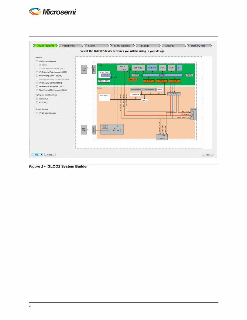
Figure 1 • IGLOO2 System Builder
4
5
1 – Accessing System Builder
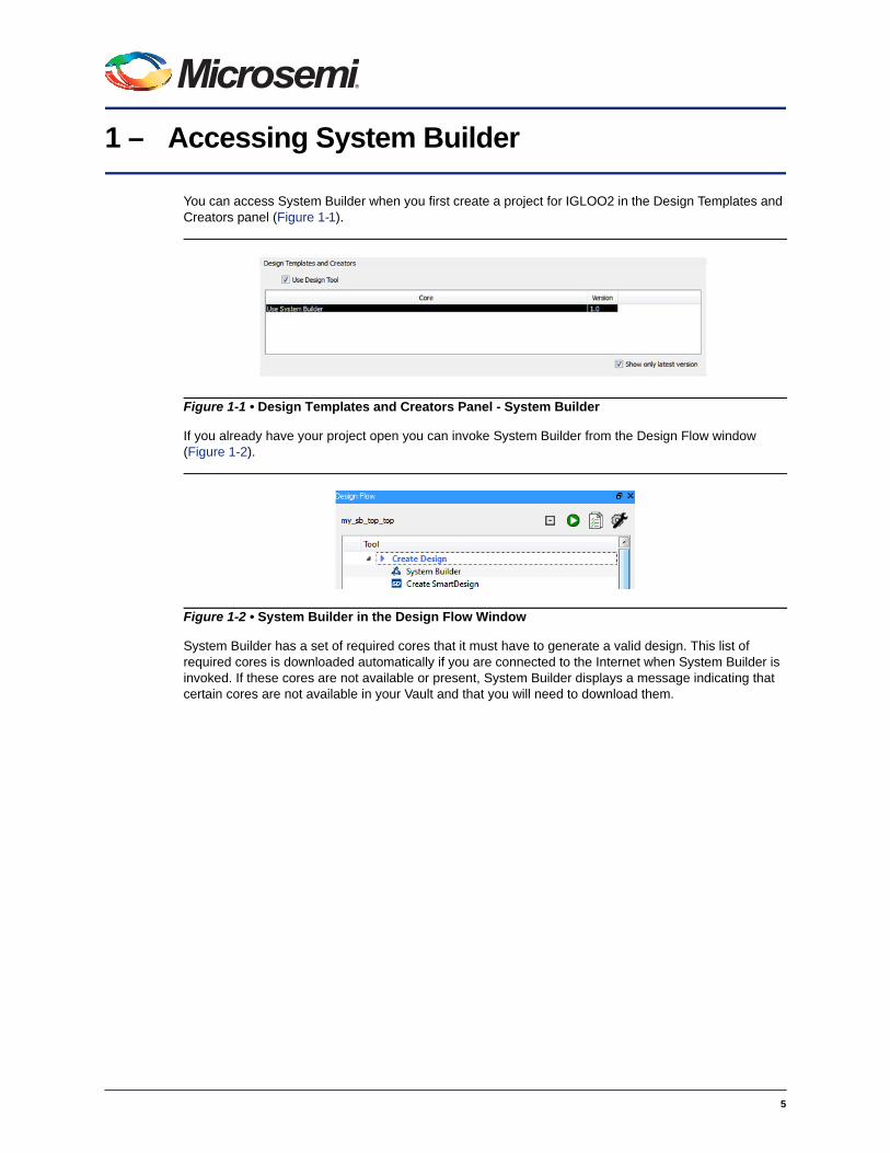
You can access System Builder when you first create a project for IGLOO2 in the Design Templates and Creators panel (Figure 1-1).
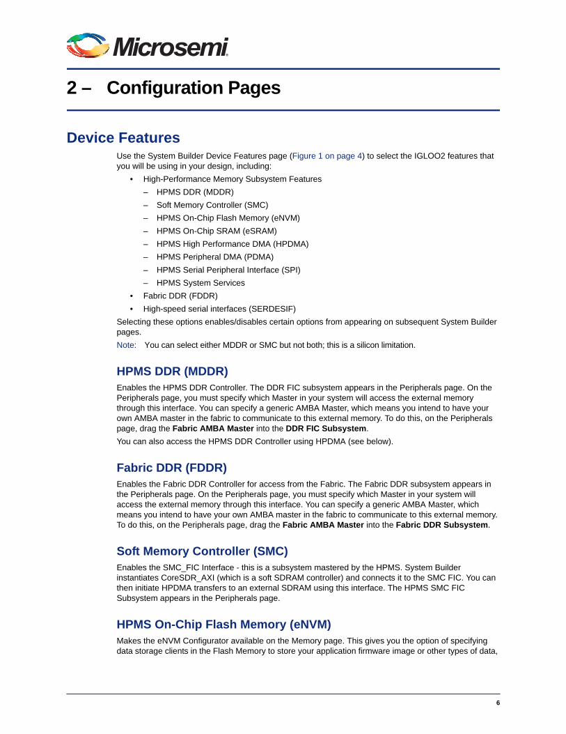
If you already have your project open you can invoke System Builder from the Design Flow window (Figure 1-2).
System Builder has a set of required cores that it must have to generate a valid design. This list of required cores is downloaded automatically if you are connected to the Internet when System Builder is invoked. If these cores are not available or present, System Builder displays a message indicating that certain cores are not available in your Vault and that you will need to download them.
Figure 1-1 • Design Templates and Creators Panel - System Builder
Figure 1-2 • System Builder in the Design Flow Window
2 – Configuration Pages
Device FeaturesUse the System Builder Device Features page (Figure 1 on page 4) to select the IGLOO2 features that you will be using in your design, including:
• High-Performance Memory Subsystem Features
– HPMS DDR (MDDR)
– Soft Memory Controller (SMC)
– HPMS On-Chip Flash Memory (eNVM)
– HPMS On-Chip SRAM (eSRAM)
– HPMS High Performance DMA (HPDMA)
– HPMS Peripheral DMA (PDMA)
– HPMS Serial Peripheral Interface (SPI)
– HPMS System Services
• Fabric DDR (FDDR)
• High-speed serial interfaces (SERDESIF)
Selecting these options enables/disables certain options from appearing on subsequent System Builder pages.
Note: You can select either MDDR or SMC but not both; this is a silicon limitation.
HPMS DDR (MDDR)Enables the HPMS DDR Controller. The DDR FIC subsystem appears in the Peripherals page. On the Peripherals page, you must specify which Master in your system will access the external memory through this interface. You can specify a generic AMBA Master, which means you intend to have your own AMBA master in the fabric to communicate to this external memory. To do this, on the Peripherals page, drag the Fabric AMBA Master into the DDR FIC Subsystem.
You can also access the HPMS DDR Controller using HPDMA (see below).
Fabric DDR (FDDR)Enables the Fabric DDR Controller for access from the Fabric. The Fabric DDR subsystem appears in the Peripherals page. On the Peripherals page, you must specify which Master in your system will access the external memory through this interface. You can specify a generic AMBA Master, which means you intend to have your own AMBA master in the fabric to communicate to this external memory. To do this, on the Peripherals page, drag the Fabric AMBA Master into the Fabric DDR Subsystem.
Soft Memory Controller (SMC)Enables the SMC_FIC Interface - this is a subsystem mastered by the HPMS. System Builder instantiates CoreSDR_AXI (which is a soft SDRAM controller) and connects it to the SMC FIC. You can then initiate HPDMA transfers to an external SDRAM using this interface. The HPMS SMC FIC Subsystem appears in the Peripherals page.
HPMS On-Chip Flash Memory (eNVM)Makes the eNVM Configurator available on the Memory page. This gives you the option of specifying data storage clients in the Flash Memory to store your application firmware image or other types of data,
6
such as data co-efficients or serialization clients. In addition, a port for a Fabric Master is exposed. You can connect your Fabric AMBA Master to this port to access the eNVM.
HPMS On-Chip SRAM (eSRAM)Exposes a port for a Fabric Master. You can connect your Fabric AMBA Master to this port to access the eSRAM.
HPMS High-Performance DMA (HPDMA)The IGLOO2 High-Performance DMA module enables you to initiate transfers between the HPMS DDR at one end and eSRAM/eNVM (read only)/Fabric Slaves at the other end. This option exposes a port for a Fabric Master. You must connect your Fabric AMBA Master to this port to access the HPDMA configuration registers. For details, refer to the IGLOO2 Silicon User’s Guide.
Note: If you want a Fabric peripheral to participate in HPDMA transfers, you must add it to an HPMS Master Subsystem on the Peripherals page.
If you want to use the Soft Memory Controller (SMC) you must also select HPDMA.
If you select and check HPDMA in the Device Features page, the HPDMA block is automatically brought out of reset at Power Up.
HPMS Peripheral DMA (PDMA)The IGLOO2 High-Performance DMA module allows you to initiate transfers between any of the following HPMS/Fabric peripherals:
• eNVM (Read only)
• eSRAM
• Fabric Peripherals
This option exposes a port for a Fabric Master. You must connect your Fabric AMBA Master to this port to access the PDMA configuration registers. For details, refer to the IGLOO2 Silicon User’s Guide.
Note: If you want a Fabric peripheral to participate in PDMA transfers, you must add it to an HPMS Master Subsystem on the Peripherals page.
HPMS Serial Peripheral Interface (SPI)Enables the HPMS SPI. You can access an external flash memory using this interface. Selecting this option exposes a port for a Fabric Master. You must connect your Fabric AMBA Master to this port to access the HPMS SPI configuration registers. For details, refer to the IGLOO2 FPGA High Performance Memory Subsystem User's Guide.
HPMS System ServicesThe IGLOO2 HPMS offers you a variety of Services, including Random Number Generation, Encryption and Flash*Freeze. To access these services, you must:
1. Check the HPMS System Services checkbox in the Device Features page in System Builder. This exposes a Fabric Master port on the System Builder generated block.
2. In SmartDesign, instantiate and configure the CoreSysServices soft IP core from the Catalog and connect it to this exposed port.
Note: If you use System Services, you cannot use any of the eSRAM, eNVM, PDMA and HPDMA, and vice versa. This will be fixed in a later release.
High-speed Serial InterfacesDepending on the device, you can select up to four SERDES interfaces. If you select a SERDES interface on this page, System Builder builds the configuration subsystem for your SERDES interface.
7
You still need to instantiate and connect the SERDES interface using SmartDesign. For details, refer to the SERDES Configurator User’s Guide.
Libero automatically stores SERDES configuration data from the SERDES Configurator in the eNVM. Upon system reset, this configuration data is automatically copied into the appropriate configuration registers of the SERDES over the APB connection from the System Builder component to the SERDESIF module.
Refer to the IGLOO2 High Speed Serial Interfaces and User's Guide for a complete description of all the SERDES options and registers.
MemoryThis page is available if you are using the HPMS DDR (MDDR), Fabric DDR (FDDR), or the embedded Flash Memory (eNVM). It enables you to configure the memory components listed below.
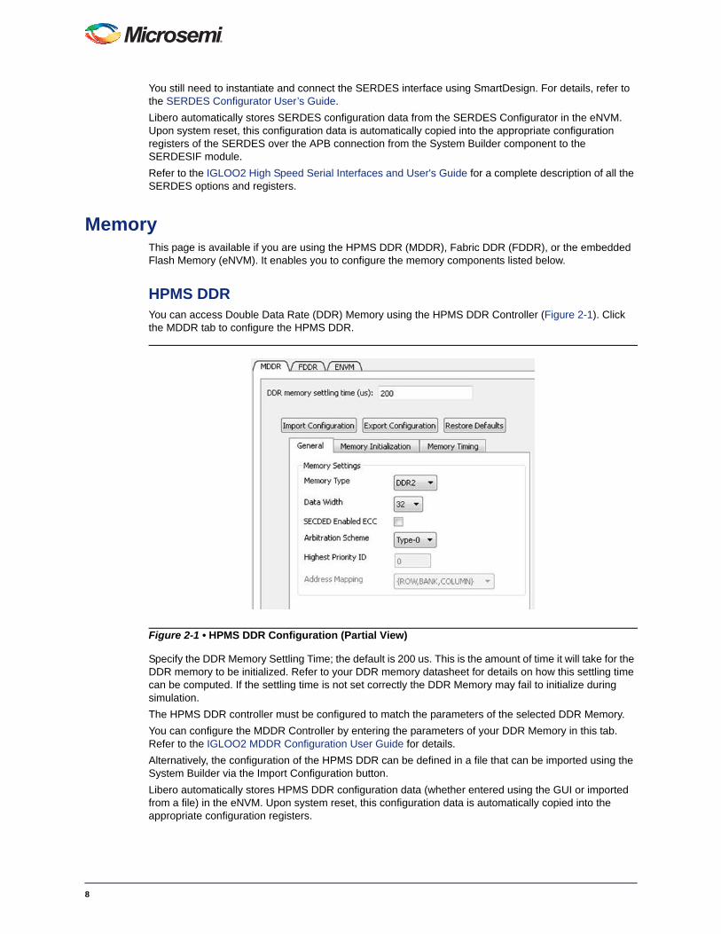
HPMS DDRYou can access Double Data Rate (DDR) Memory using the HPMS DDR Controller (Figure 2-1). Click the MDDR tab to configure the HPMS DDR.
Specify the DDR Memory Settling Time; the default is 200 us. This is the amount of time it will take for the DDR memory to be initialized. Refer to your DDR memory datasheet for details on how this settling time can be computed. If the settling time is not set correctly the DDR Memory may fail to initialize during simulation.
The HPMS DDR controller must be configured to match the parameters of the selected DDR Memory.
You can configure the MDDR Controller by entering the parameters of your DDR Memory in this tab. Refer to the IGLOO2 MDDR Configuration User Guide for details.
Alternatively, the configuration of the HPMS DDR can be defined in a file that can be imported using the System Builder via the Import Configuration button.
Libero automatically stores HPMS DDR configuration data (whether entered using the GUI or imported from a file) in the eNVM. Upon system reset, this configuration data is automatically copied into the appropriate configuration registers.
Figure 2-1 • HPMS DDR Configuration (Partial View)
8
Refer to the IGLOO2 DDR Interfaces User's Guide for a complete description of all the DDR configuration options and registers.
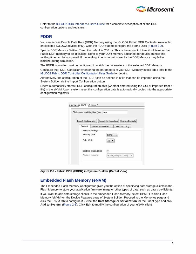
FDDRYou can access Double Data Rate (DDR) Memory using the IGLOO2 Fabric DDR Controller (available on selected IGLOO2 devices only). Click the FDDR tab to configure the Fabric DDR (Figure 2-2).
Specify DDR Memory Settling Time; the default is 200 us. This is the amount of time it will take for the Fabric DDR memory to be initialized. Refer to your DDR memory datasheet for details on how this settling time can be computed. If the settling time is not set correctly the DDR Memory may fail to initialize during simulation.
The FDDR controller must be configured to match the parameters of the selected DDR Memory.
Configure the FDDR Controller by entering the parameters of your DDR Memory in this tab. Refer to the IGLOO2 Fabric DDR Controller Configuration User Guide for details.
Alternatively, the configuration of the FDDR can be defined in a file that can be imported using the System Builder via the Import Configuration button.
Libero automatically stores FDDR configuration data (whether entered using the GUI or imported from a file) in the eNVM. Upon system reset this configuration data is automatically copied into the appropriate configuration registers.
Embedded Flash Memory (eNVM)The Embedded Flash Memory Configurator gives you the option of specifying data storage clients in the Flash Memory to store your application firmware image or other types of data, such as data co-efficients.
If you want to add data storage clients to the embedded Flash Memory, select HPMS On-chip Flash Memory (eNVM) on the Device Features page of System Builder. Proceed to the Memories page and click the ENVM tab to configure it. Select the Data Storage or Serialization for the Client type and click Add to System. (Figure 2-3). Click Edit to modify the configuration of your eNVM client.
Figure 2-2 • Fabric DDR (FDDR) in System Builder (Partial View)
9
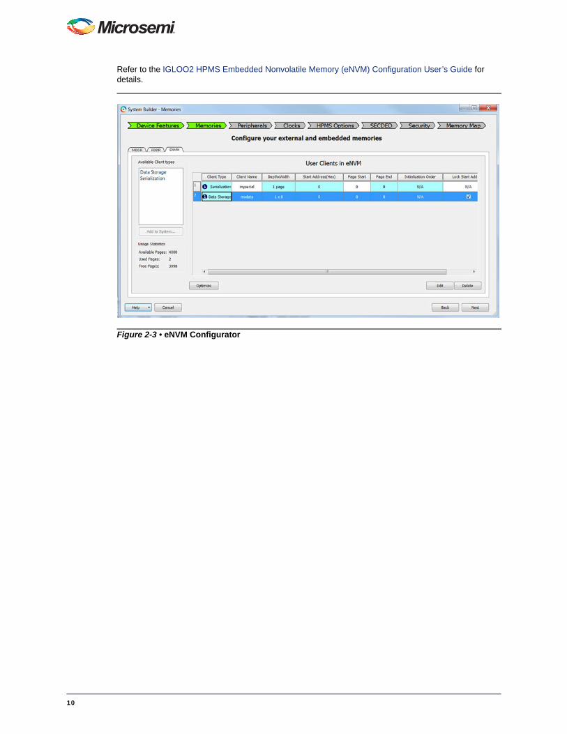
Refer to the IGLOO2 HPMS Embedded Nonvolatile Memory (eNVM) Configuration User’s Guide for details.
Figure 2-3 • eNVM Configurator
10
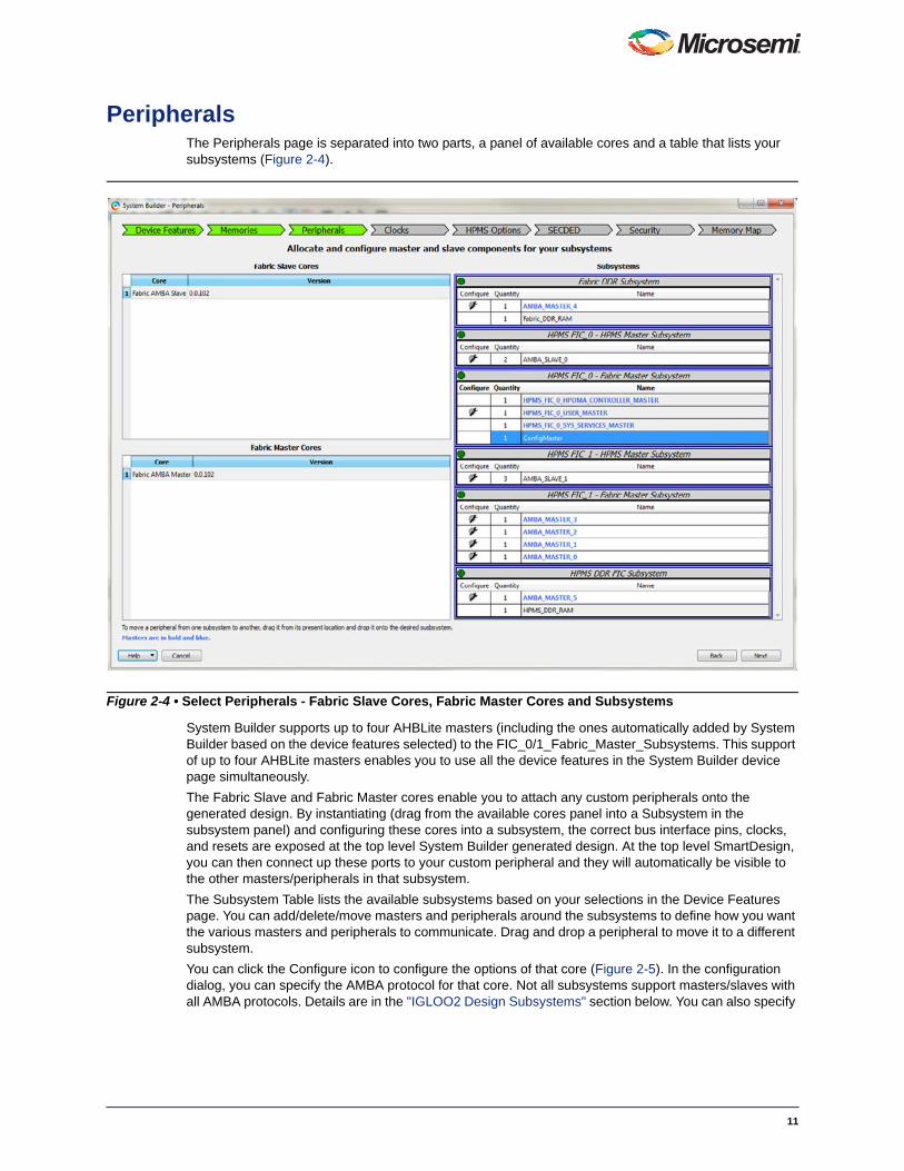
PeripheralsThe Peripherals page is separated into two parts, a panel of available cores and a table that lists your subsystems (Figure 2-4).
System Builder supports up to four AHBLite masters (including the ones automatically added by System Builder based on the device features selected) to the FIC_0/1_Fabric_Master_Subsystems. This support of up to four AHBLite masters enables you to use all the device features in the System Builder device page simultaneously.
The Fabric Slave and Fabric Master cores enable you to attach any custom peripherals onto the generated design. By instantiating (drag from the available cores panel into a Subsystem in the subsystem panel) and configuring these cores into a subsystem, the correct bus interface pins, clocks, and resets are exposed at the top level System Builder generated design. At the top level SmartDesign, you can then connect up these ports to your custom peripheral and they will automatically be visible to the other masters/peripherals in that subsystem.
The Subsystem Table lists the available subsystems based on your selections in the Device Features page. You can add/delete/move masters and peripherals around the subsystems to define how you want the various masters and peripherals to communicate. Drag and drop a peripheral to move it to a different subsystem.
You can click the Configure icon to configure the options of that core (Figure 2-5). In the configuration dialog, you can specify the AMBA protocol for that core. Not all subsystems support masters/slaves with all AMBA protocols. Details are in the "IGLOO2 Design Subsystems" section below. You can also specify
Figure 2-4 • Select Peripherals - Fabric Slave Cores, Fabric Master Cores and Subsystems
11
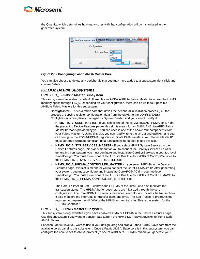
the Quantity, which determines how many cores with that configuration will be instantiated in the generated system.
You can also choose to delete any peripherals that you may have added to a subsystem; right-click and choose Delete.
IGLOO2 Design SubsystemsHPMS FIC_0 - Fabric Master SubsystemThis subsystem is available by default. It enables an AMBA AHBLite Fabric Master to access the HPMS memory space through FIC_0. Depending on your configuration, there can be up to four possible AHBLite Fabric Masters for this subsystem.
• ConfigMaster - This is a fabric core that drives the peripheral initialization process (i.e., the process of copying register configuration data from the eNVM to the DDR/SERDES). ConfigMaster is completely managed by System Builder, and you cannot modify it.
– HPMS_FIC_0_USER_MASTER- If you select one of the eNVM, eSRAM, PDMA, or SPI (in the preceding Device Features page), this slot is meant for an AMBA AHBLite/APB3 Fabric Master IP that is provided by you. You can access one of the above four components from your Fabric Master IP. Using this slot, you can read/write to the eNVM and eSRAM, and you can configure the PDMA/HPDMA registers to initiate DMA transfers. Your Fabric Master IP must generate AHBLite-compliant data transactions to be able to use this slot.
– HPMS_FIC_0_SYS_SERVICES_MASTER - If you select HPMS System Services in the Device Features page, this slot is meant for you to connect the CoreSysServices IP. After generating your system, you must configure and instantiate CoreSysServices in your top level SmartDesign. You must then connect the AHBLite Bus Interface (BIF) of CoreSysServices to the HPMS_FIC_0_SYS_SERVICES_MASTER slot.
– HPMS_FIC_0_HPDMA_CONTROLLER_MASTER - If you select HPDMA in the Device Features page, this slot is meant for you to connect the CoreHPDMACtrl IP. After generating your system, you must configure and instantiate CoreHPDMACtrl in your top level SmartDesign. You must then connect the AHBLite Bus Interface (BIF) of CoreHPDMACtrl to the HPMS_FIC_0_HPDMA_CONTROLLER_MASTER slot.
The CoreHPDMACtrl Soft IP controls the HPDMA of the HPMS and also monitors the transaction status. The HPDMA buffer descriptors are initialized through the core configuration. The CoreHPDMACtrl selects the buffer descriptor and initiates the transactions. It also monitors the interrupts for transfer done and error. The Soft IP also re-programs the registers to prepare the HPDMA of the HPMS for next transfer. This is the system for the HPDMA Controller.
HPMS FIC_0 - HPMS Master SubsystemThis subsystem is only available if you have enabled PDMA or HPDMA in the Device Features page. Use this subsystem if you want to transfer data to/from the HPMS DDR/eNVM/eSRAM to/from Fabric AMBA Slaves.
For each Fabric Slave you want to use in your design, drag and drop a Fabric AMBA Slave core from the available cores panel to this subsystem. Once a Fabric AMBA Slave core is in this subsystem, you can configure the core to set its AMBA protocol (to one of AHBLite/APB3/AXI). When you generate your
Figure 2-5 • Configuring Fabric AMBA Master Core
12
system, you get an AMBA BIF (corresponding to the protocol you selected). In the top level SmartDesign, instantiate your actual Fabric Slave, and connect it to the appropriate slot in the generated system.
HPMS FIC_1 - HPMS Master SubsystemThis subsystem is only available on the M2GL050, 100, and 150 devices, and only if you have enabled PDMA or HPDMA in the Device Features page. Use this subsystem if you want to transfer data to/from the HPMS DDR/eNVM/eSRAM to/from Fabric AMBA Slaves.
For each Fabric Slave you want to use in your design, drag and drop a Fabric AMBA Slave core from the available cores panel to this subsystem. Once a Fabric AMBA Slave core is in this subsystem, you can configure the core to set its AMBA protocol (to one of AHBLite/APB3/AXI). When you generate your system, you get an AMBA BIF (corresponding to the protocol you selected). In the top level SmartDesign, instantiate your actual Fabric Slave, and connect it to the appropriate slot in the generated system.
HPMS FIC_1 - Fabric Master SubsystemThis subsystem is available by default on the M2GL050, 100, and 150 devices. It enables a Fabric Master to access the HPMS memory space through FIC_1 in addition to other Fabric peripherals.
You can drag a Fabric AMBA Master core (from the Cores pane on the Peripherals page) into this subsystem and then connect your actual Fabric Master IP to the resultant design. This subsystem supports up to four AHBLite-compliant masters.
You can configure your Fabric AMBA Master core to one of AHBLite/APB3 to correspond to your Fabric Master IP. Using your Fabric Master, you can access the eNVM and eSRAM, and the PDMA or HPDMA configuration registers inside the HPMS.
You can use the FIC_1 Fabric Master Subsystem to access HPMS features such as:
• HPMS Services (Add an AHBLite Fabric AMBA Master Core in System Builder and connect to CoreSysServices)
• eSRAM/eNVM/PDMA/HPDMA/SPI (Using your own AMBA-compliant Fabric Master)
Note: If you instantiate an APB3 Fabric Master in your FIC_1 Fabric Master Subsystem, System Builder configures the FIC_1 interface and the corresponding CoreAPB3 to be compatible with CoreABC-like APB3 Fabric Masters. In other words, System Builder automatically configures the APB3 Fabric Master interface with the following characteristics:
• 32-bit data bus
• 20 bits of address
– Lower 16 bits passed directly to the HPMS
– Upper 4 bits select 1 of 16 APB slave slots
Slot 0 - HPMS
Slots 1-14 - Fabric Slaves
Slot 15 - Indirect Addressing register
To access different HPMS address spaces, your Fabric Master must first write the base address (32-bits, lower 16 bits set to zero) into the Indirect Addressing register. For any subsequent transactions on this interface, the address "seen" by the HPMS will consist of the upper 16 bits stored in the Indirect Addressing register and the lower 16 bits driven by the User Fabric Master.
HPMS DDR FIC SubsystemThis subsystem is available if you selected the HPMS DDR feature on the Device Features page. Use this subsystem to access the HPMS DDR Memory using an AXI/AHBLite User Fabric Master. The HPMS_DDR_RAM peripheral (corresponding to the HPMS DDR controller) is shown automatically in this subsystem. You must drag and drop a Fabric AMBA Master core into this subsystem to access the HPMS DDR. When you generate your system, you get a BIF where you must connect your actual Fabric Master IP in the top level SmartDesign.
Fabric DDR SubsystemThis subsystem is available if you select the Fabric DDR feature on the Device Features page. The Fabric_DDR_RAM peripheral is automatically shown in this subsystem. You must provide a fabric master for the Fabric_DDR_RAM. This can be done in two ways:
13
If you intend to have a Fabric Master access the Fabric DDR, then you click and drag a Fabric AMBA Master core into this subsystem from the available cores list. When you generate your system, you get a BIF where you must connect your actual Fabric Master IP in the top level SmartDesign.
If you want to access the Fabric DDR RAM from another subsystem, you can also click and drag the Fabric_DDR_RAM peripheral into one of the HPMS FIC_0/1 subsystems. This action eliminates the Fabric DDR Subsystem and makes the Fabric DDR Controller part of the HPMS FIC subsystem you dragged it into. The Master of the Fabric DDR will now be the same as the master of the HPMS FIC subsystem it is in (i.e., one of PDMA/HPDMA or a Fabric Master). If you do this, on the Clocks page, you must set the FDDR_SUBSYSTEM_CLK frequency to be equal to the frequency of FIC_0/1_CLK (depending on whether you dropped the Fabric_DDR_RAM in a FIC_0 or FIC_1 subsystem).
You can also click and drag the Fabric_DDR_RAM peripheral into the HPMS_DDR_FIC_SUBSYSTEM. This eliminates the Fabric DDR Subsystem and makes the Fabric DDR Controller part of the HPMS DDR FIC subsystem. The master of the Fabric DDR will now be the same as the master of the HPMS_DDR. If you do this, you must also drag and drop a Fabric AMBA Master core into the HPMS_DDR_FIC_SUBSYSTEM. When you generate your system, you get a BIF where you must connect your actual Fabric Master IP in the top level SmartDesign. Also, on the Clocks page, you must set the FDDR_SUBSYSTEM_CLK frequency to be equal to the frequency of DDR/SMC_FIC_CLK.
HPMS SMC FIC SubsystemThis subsystem is available in the Peripherals Page if you select the SMC (Soft Memory Controller) in the Device Features page. HPMS High Performance DMA (HPDMA) is selected automatically in the Device Features Page if you select SMC.
Use the IGLOO2 Soft Memory Controller Fabric Interface Controller (SMC_FIC) to access external bulk memories other than DDR, such as SDRAM. The HPDMA controller accesses external Single Data Rate DRAM or Asynchronous memories via this SMC_FIC and a soft memory controller instantiated in the FPGA fabric such as CoreSDR_AXI and CoreSDR_AHB. It also manages data transfers to and from eSRAM/eNVM/Fabric Slaves.
Click the ‘Configure’ icon next to the HPMS_SMC instance in the Peripherals page to configure the specific external memory parameters (width, timing, etc.), as shown in Figure 2-6 below.
System Builder exposes the SMC interface ports(HPMS_SMC_0_PINS) to the top level.
If the SMC_FIC is enabled, the MDDR subsystem is not available. In SMC_FIC mode, the DDR I/O’s associated with the MDDR subsystem are released and are available as general FPGA Fabric I/O’s.
Note: To use the HPMS SMC, you must select SMC and HPMS High Performance DMA (HPDMA) in the Device Features page.
System Builder automatically instantiates the IP Core CoreSDR_AXI as a Soft Memory Controller (SMC) to build the System Builder block. Click the Configure icon of the HPMS SMC FIC subsystem in the
14
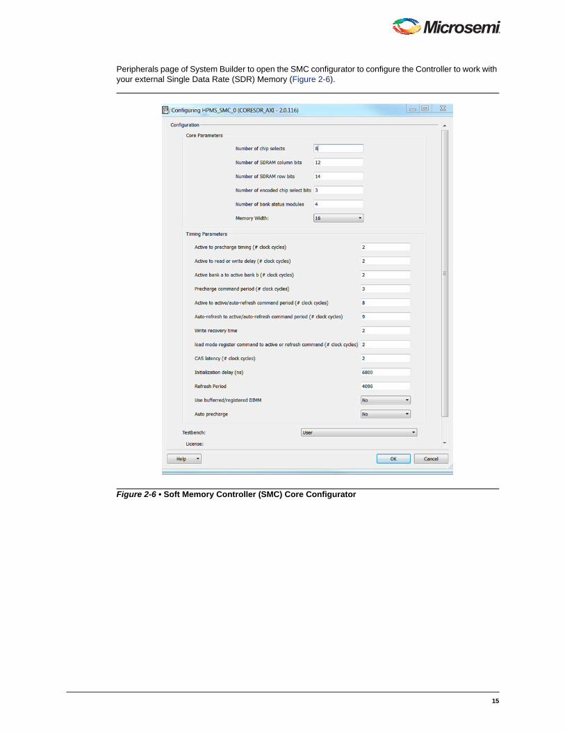
Peripherals page of System Builder to open the SMC configurator to configure the Controller to work with your external Single Data Rate (SDR) Memory (Figure 2-6).
Figure 2-6 • Soft Memory Controller (SMC) Core Configurator
15
Clock The Clocks page enables you to enter and configure clock parameters for your systems. There are three tabs in the Clocks page:
• Clock
• Fabric CCC
• Chip Oscillators
Clock TabSystem Clock - The System Builder automatically instantiates the required PLL (if needed).
The following controls enable you to specify the System Clock, your clock source options include:
• FPGA Fabric Input
• Dedicated Input Pad
• On-chip 1 MHz RC Oscillator
• On-chip 25/50 MHz RC Oscillator
• External Main Crystal Oscillator (Ceramic Resonator 0.5MHz to 4MHz)
• External Main Crystal Oscillator (Crystal 32KHz - 20MHz)
• External Main Crystal Oscillator (RC Network 32KHz - 4MHz)
Your clock source options determine what frequency you can specify. The other clocks in the system are derived from the System Clock setting. The tool enforces these dependency rules. Refer to the CCC Configuration Guide for more detailed information on Clock Settings.
HPMS Clock - Specifies how fast you want your HPMS base clock to run. This specifies the frequency of the eNVM and eSRAM
MDDR Clocks - Consists of two clock domains: MDDR_CLK and DDR/SMC_FIC_CLK. The MDDR_CLK specifies how fast your HPMS DDR RAM runs, this refers to the DDR I/O side of the DDR controller. The DDR/SMC _FIC_CLK option specifies the frequency at which your fabric logic (including your Fabric Master) interfaces with the HPMS DDR controller.
Fabric Interface Clocks - The FIC_0_CLK is the frequency at which the HPMS FIC_0 subsystems operate. The FIC_1_CLK is the frequency at which the HPMS FIC_1 subsystems operate. If the FIC clocks are grayed out, it means you have not added any peripherals to those subsystems in the Peripherals page and there is no need to set clock frequencies for these subsystems.
Fabric DDR Clocks - The FDDR_CLK specifies how fast your Fabric DDR RAM runs. It refers to the DDR I/O side of the DDR controller. The FDDR_SUBSYSTEM_CLK is the frequency at which your fabric
16
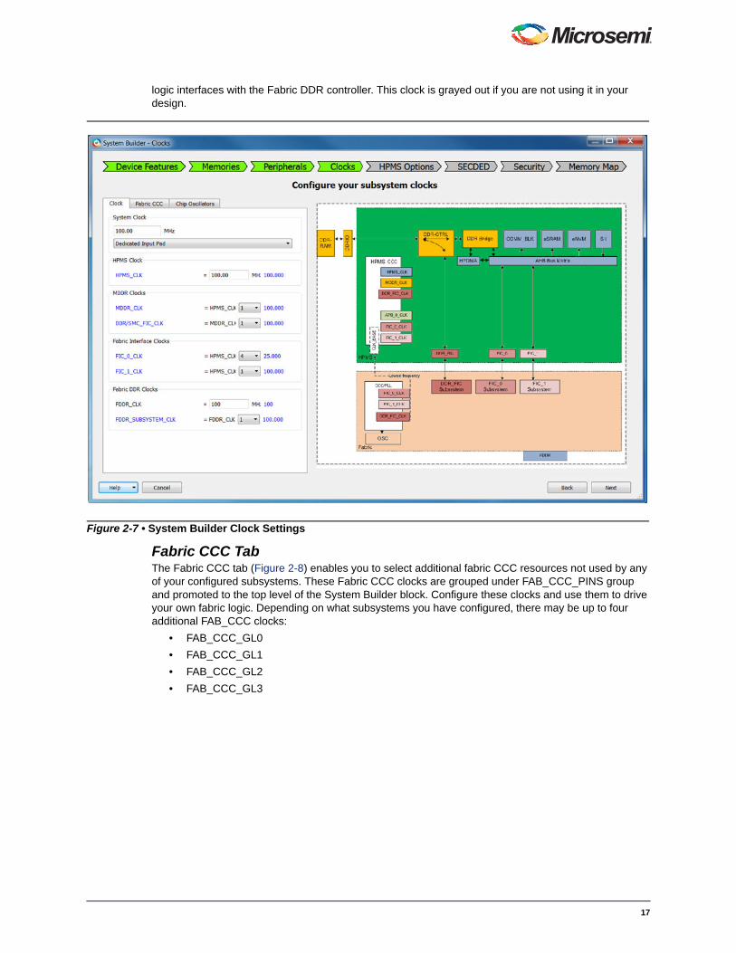
logic interfaces with the Fabric DDR controller. This clock is grayed out if you are not using it in your design.
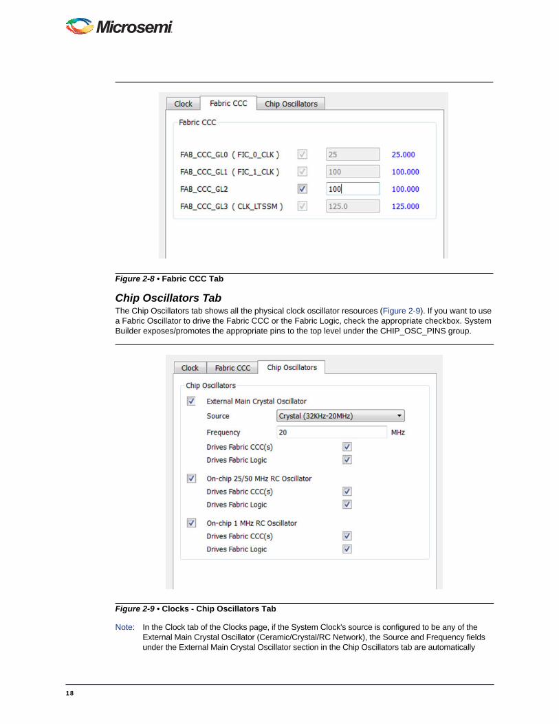
Fabric CCC TabThe Fabric CCC tab (Figure 2-8) enables you to select additional fabric CCC resources not used by any of your configured subsystems. These Fabric CCC clocks are grouped under FAB_CCC_PINS group and promoted to the top level of the System Builder block. Configure these clocks and use them to drive your own fabric logic. Depending on what subsystems you have configured, there may be up to four additional FAB_CCC clocks:
• FAB_CCC_GL0
• FAB_CCC_GL1
• FAB_CCC_GL2
• FAB_CCC_GL3
Figure 2-7 • System Builder Clock Settings
17
Chip Oscillators TabThe Chip Oscillators tab shows all the physical clock oscillator resources (Figure 2-9). If you want to use a Fabric Oscillator to drive the Fabric CCC or the Fabric Logic, check the appropriate checkbox. System Builder exposes/promotes the appropriate pins to the top level under the CHIP_OSC_PINS group.
Note: In the Clock tab of the Clocks page, if the System Clock's source is configured to be any of the External Main Crystal Oscillator (Ceramic/Crystal/RC Network), the Source and Frequency fields under the External Main Crystal Oscillator section in the Chip Oscillators tab are automatically
Figure 2-8 • Fabric CCC Tab
Figure 2-9 • Clocks - Chip Oscillators Tab
18
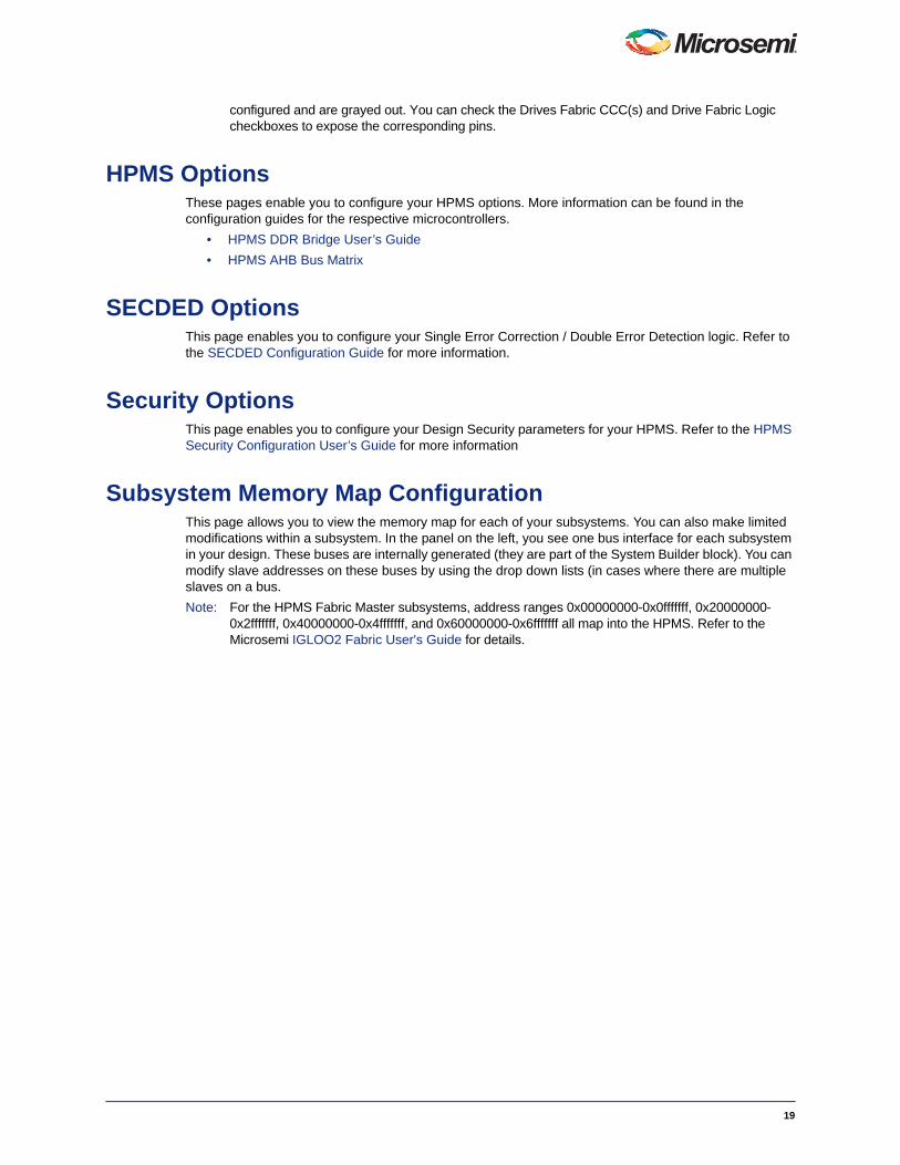
configured and are grayed out. You can check the Drives Fabric CCC(s) and Drive Fabric Logic checkboxes to expose the corresponding pins.
HPMS OptionsThese pages enable you to configure your HPMS options. More information can be found in the configuration guides for the respective microcontrollers.
• HPMS DDR Bridge User’s Guide
• HPMS AHB Bus Matrix
SECDED OptionsThis page enables you to configure your Single Error Correction / Double Error Detection logic. Refer to the SECDED Configuration Guide for more information.
Security OptionsThis page enables you to configure your Design Security parameters for your HPMS. Refer to the HPMS Security Configuration User’s Guide for more information
Subsystem Memory Map ConfigurationThis page allows you to view the memory map for each of your subsystems. You can also make limited modifications within a subsystem. In the panel on the left, you see one bus interface for each subsystem in your design. These buses are internally generated (they are part of the System Builder block). You can modify slave addresses on these buses by using the drop down lists (in cases where there are multiple slaves on a bus.
Note: For the HPMS Fabric Master subsystems, address ranges 0x00000000-0x0fffffff, 0x20000000-0x2fffffff, 0x40000000-0x4fffffff, and 0x60000000-0x6fffffff all map into the HPMS. Refer to the Microsemi IGLOO2 Fabric User's Guide for details.
19
3 – Generating Your System
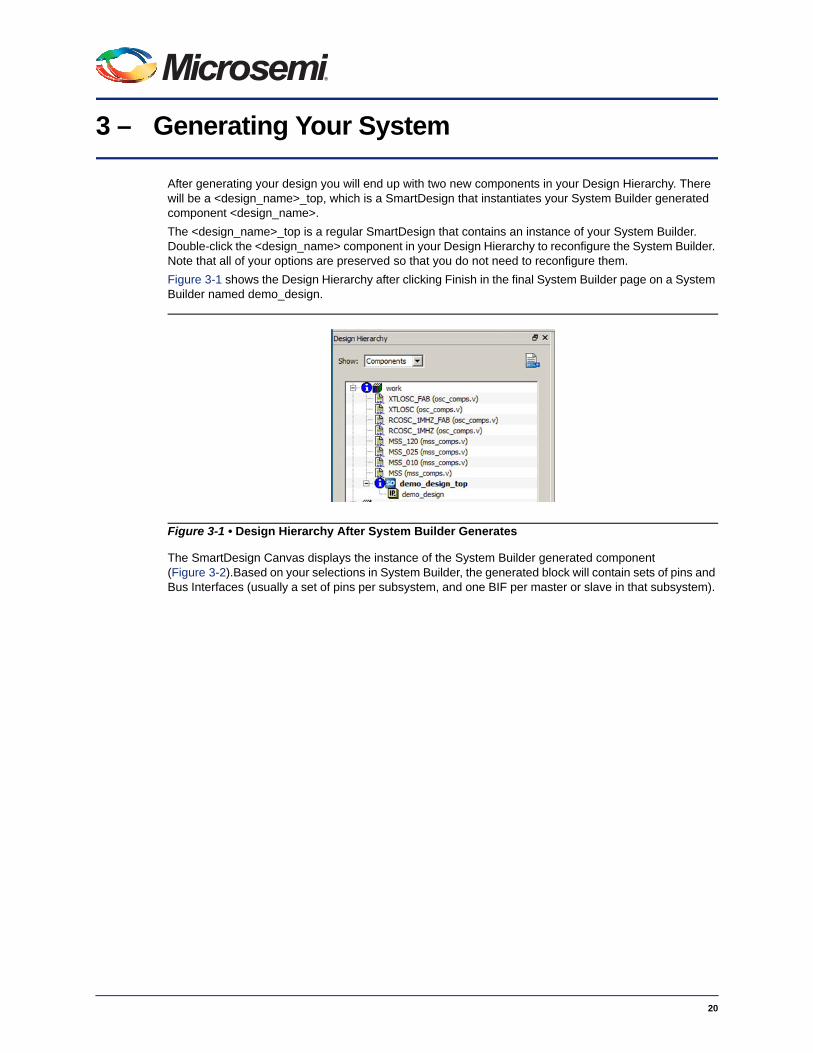
After generating your design you will end up with two new components in your Design Hierarchy. There will be a <design_name>_top, which is a SmartDesign that instantiates your System Builder generated component <design_name>.
The <design_name>_top is a regular SmartDesign that contains an instance of your System Builder. Double-click the <design_name> component in your Design Hierarchy to reconfigure the System Builder. Note that all of your options are preserved so that you do not need to reconfigure them.
Figure 3-1 shows the Design Hierarchy after clicking Finish in the final System Builder page on a System Builder named demo_design.
The SmartDesign Canvas displays the instance of the System Builder generated component (Figure 3-2).Based on your selections in System Builder, the generated block will contain sets of pins and Bus Interfaces (usually a set of pins per subsystem, and one BIF per master or slave in that subsystem).
Figure 3-1 • Design Hierarchy After System Builder Generates
20
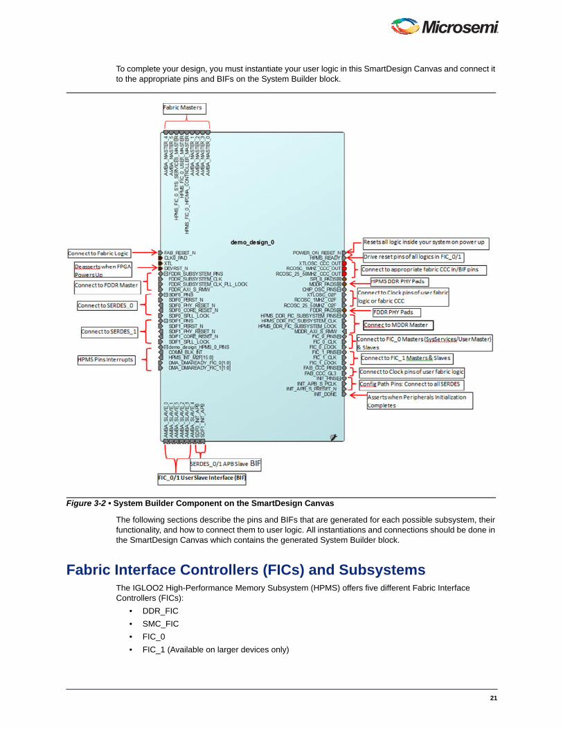
To complete your design, you must instantiate your user logic in this SmartDesign Canvas and connect it to the appropriate pins and BIFs on the System Builder block.
The following sections describe the pins and BIFs that are generated for each possible subsystem, their functionality, and how to connect them to user logic. All instantiations and connections should be done in the SmartDesign Canvas which contains the generated System Builder block.
Fabric Interface Controllers (FICs) and SubsystemsThe IGLOO2 High-Performance Memory Subsystem (HPMS) offers five different Fabric Interface Controllers (FICs):
• DDR_FIC
• SMC_FIC
• FIC_0
• FIC_1 (Available on larger devices only)
Figure 3-2 • System Builder Component on the SmartDesign Canvas
21
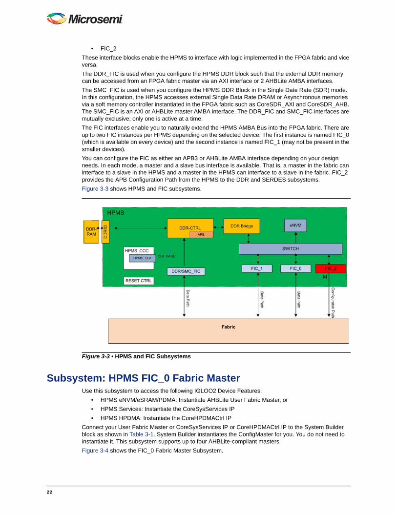
• FIC_2
These interface blocks enable the HPMS to interface with logic implemented in the FPGA fabric and vice versa.
The DDR_FIC is used when you configure the HPMS DDR block such that the external DDR memory can be accessed from an FPGA fabric master via an AXI interface or 2 AHBLite AMBA interfaces.
The SMC_FIC is used when you configure the HPMS DDR Block in the Single Date Rate (SDR) mode. In this configuration, the HPMS accesses external Single Data Rate DRAM or Asynchronous memories via a soft memory controller instantiated in the FPGA fabric such as CoreSDR_AXI and CoreSDR_AHB. The SMC_FIC is an AXI or AHBLite master AMBA interface. The DDR_FIC and SMC_FIC interfaces are mutually exclusive; only one is active at a time.
The FIC interfaces enable you to naturally extend the HPMS AMBA Bus into the FPGA fabric. There are up to two FIC instances per HPMS depending on the selected device. The first instance is named FIC_0 (which is available on every device) and the second instance is named FIC_1 (may not be present in the smaller devices).
You can configure the FIC as either an APB3 or AHBLite AMBA interface depending on your design needs. In each mode, a master and a slave bus interface is available. That is, a master in the fabric can interface to a slave in the HPMS and a master in the HPMS can interface to a slave in the fabric. FIC_2 provides the APB Configuration Path from the HPMS to the DDR and SERDES subsystems.
Figure 3-3 shows HPMS and FIC subsystems.
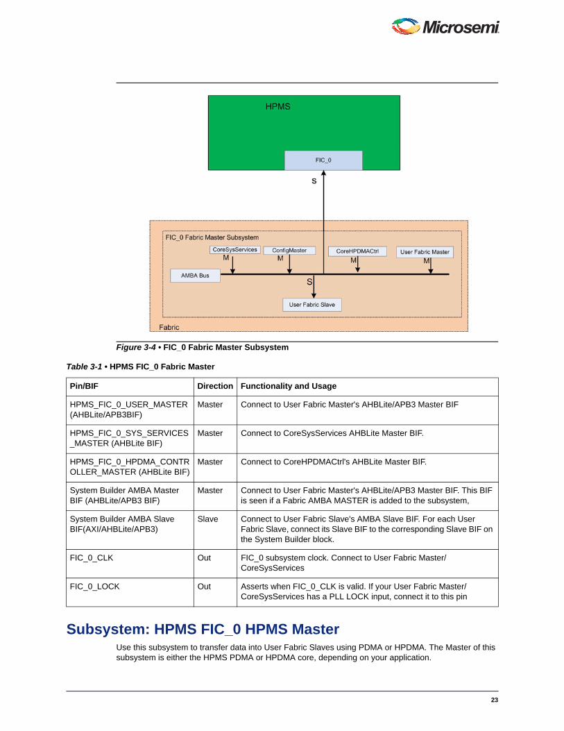
Subsystem: HPMS FIC_0 Fabric Master Use this subsystem to access the following IGLOO2 Device Features:
• HPMS eNVM/eSRAM/PDMA: Instantiate AHBLite User Fabric Master, or
• HPMS Services: Instantiate the CoreSysServices IP
• HPMS HPDMA: Instantiate the CoreHPDMACtrl IP
Connect your User Fabric Master or CoreSysServices IP or CoreHPDMACtrl IP to the System Builder block as shown in Table 3-1. System Builder instantiates the ConfigMaster for you. You do not need to instantiate it. This subsystem supports up to four AHBLite-compliant masters.
Figure 3-4 shows the FIC_0 Fabric Master Subsystem.
Figure 3-3 • HPMS and FIC Subsystems
22
Subsystem: HPMS FIC_0 HPMS MasterUse this subsystem to transfer data into User Fabric Slaves using PDMA or HPDMA. The Master of this subsystem is either the HPMS PDMA or HPDMA core, depending on your application.
Figure 3-4 • FIC_0 Fabric Master Subsystem
Table 3-1 • HPMS FIC_0 Fabric Master
Pin/BIF Direction Functionality and Usage
HPMS_FIC_0_USER_MASTER (AHBLite/APB3BIF)
Master Connect to User Fabric Master's AHBLite/APB3 Master BIF
HPMS_FIC_0_SYS_SERVICES_MASTER (AHBLite BIF)
Master Connect to CoreSysServices AHBLite Master BIF.
HPMS_FIC_0_HPDMA_CONTROLLER_MASTER (AHBLite BIF)
Master Connect to CoreHPDMACtrl's AHBLite Master BIF.
System Builder AMBA Master BIF (AHBLite/APB3 BIF)
Master Connect to User Fabric Master's AHBLite/APB3 Master BIF. This BIF is seen if a Fabric AMBA MASTER is added to the subsystem,
System Builder AMBA Slave BIF(AXI/AHBLite/APB3)
Slave Connect to User Fabric Slave's AMBA Slave BIF. For each User Fabric Slave, connect its Slave BIF to the corresponding Slave BIF on the System Builder block.
FIC_0_CLK Out FIC_0 subsystem clock. Connect to User Fabric Master/CoreSysServices
FIC_0_LOCK Out Asserts when FIC_0_CLK is valid. If your User Fabric Master/CoreSysServices has a PLL LOCK input, connect it to this pin
23
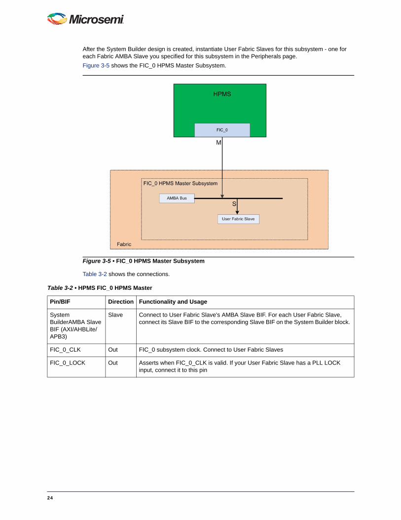
After the System Builder design is created, instantiate User Fabric Slaves for this subsystem - one for each Fabric AMBA Slave you specified for this subsystem in the Peripherals page.
Figure 3-5 shows the FIC_0 HPMS Master Subsystem.
Table 3-2 shows the connections.
Figure 3-5 • FIC_0 HPMS Master Subsystem
Table 3-2 • HPMS FIC_0 HPMS Master
Pin/BIF Direction Functionality and Usage
System BuilderAMBA Slave BIF (AXI/AHBLite/APB3)
Slave Connect to User Fabric Slave's AMBA Slave BIF. For each User Fabric Slave, connect its Slave BIF to the corresponding Slave BIF on the System Builder block.
FIC_0_CLK Out FIC_0 subsystem clock. Connect to User Fabric Slaves
FIC_0_LOCK Out Asserts when FIC_0_CLK is valid. If your User Fabric Slave has a PLL LOCK input, connect it to this pin
24
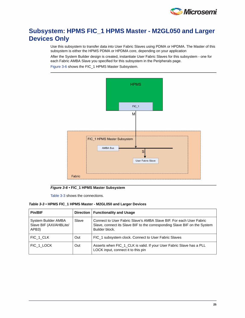
Subsystem: HPMS FIC_1 HPMS Master - M2GL050 and Larger Devices Only
Use this subsystem to transfer data into User Fabric Slaves using PDMA or HPDMA. The Master of this subsystem is either the HPMS PDMA or HPDMA core, depending on your application
After the System Builder design is created, instantiate User Fabric Slaves for this subsystem - one for each Fabric AMBA Slave you specified for this subsystem in the Peripherals page.
Figure 3-6 shows the FIC_1 HPMS Master Subsystem.
Table 3-3 shows the connections.
Figure 3-6 • FIC_1 HPMS Master Subsystem
Table 3-3 • HPMS FIC_1 HPMS Master - M2GL050 and Larger Devices
Pin/BIF Direction Functionality and Usage
System Builder AMBA Slave BIF (AXI/AHBLite/APB3)
Slave Connect to User Fabric Slave's AMBA Slave BIF. For each User Fabric Slave, connect its Slave BIF to the corresponding Slave BIF on the System Builder block.
FIC_1_CLK Out FIC_1 subsystem clock. Connect to User Fabric Slaves
FIC_1_LOCK Out Asserts when FIC_1_CLK is valid. If your User Fabric Slave has a PLL LOCK input, connect it to this pin
25
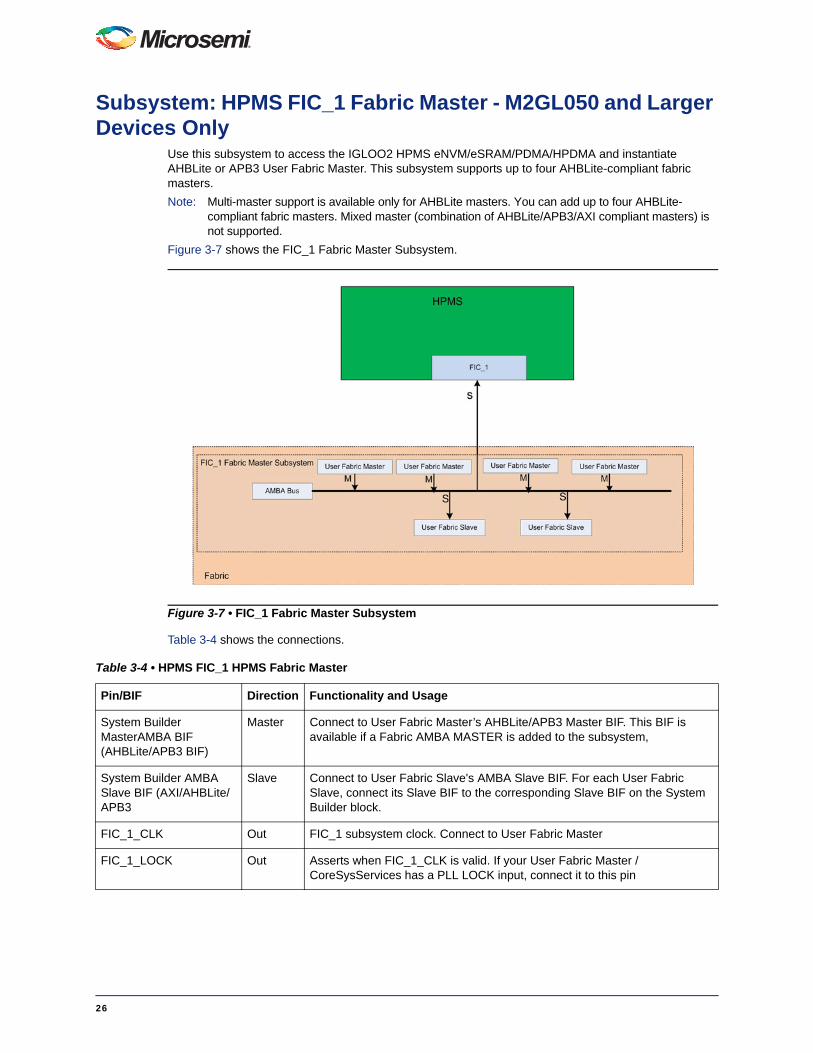
Subsystem: HPMS FIC_1 Fabric Master - M2GL050 and Larger Devices Only
Use this subsystem to access the IGLOO2 HPMS eNVM/eSRAM/PDMA/HPDMA and instantiate AHBLite or APB3 User Fabric Master. This subsystem supports up to four AHBLite-compliant fabric masters.
Note: Multi-master support is available only for AHBLite masters. You can add up to four AHBLite-compliant fabric masters. Mixed master (combination of AHBLite/APB3/AXI compliant masters) is not supported.
Figure 3-7 shows the FIC_1 Fabric Master Subsystem.
Table 3-4 shows the connections.
Figure 3-7 • FIC_1 Fabric Master Subsystem
Table 3-4 • HPMS FIC_1 HPMS Fabric Master
Pin/BIF Direction Functionality and Usage
System Builder MasterAMBA BIF (AHBLite/APB3 BIF)
Master Connect to User Fabric Master’s AHBLite/APB3 Master BIF. This BIF is available if a Fabric AMBA MASTER is added to the subsystem,
System Builder AMBA Slave BIF (AXI/AHBLite/APB3
Slave Connect to User Fabric Slave's AMBA Slave BIF. For each User Fabric Slave, connect its Slave BIF to the corresponding Slave BIF on the System Builder block.
FIC_1_CLK Out FIC_1 subsystem clock. Connect to User Fabric Master
FIC_1_LOCK Out Asserts when FIC_1_CLK is valid. If your User Fabric Master / CoreSysServices has a PLL LOCK input, connect it to this pin
26
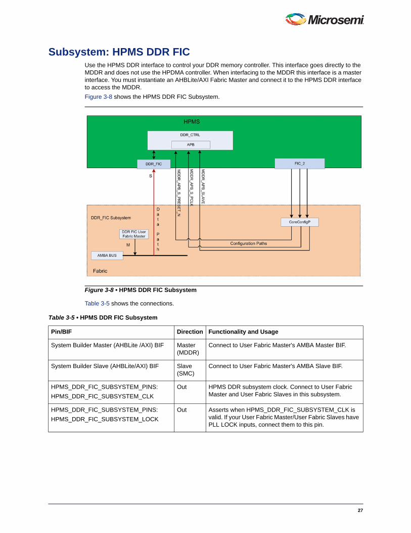
Subsystem: HPMS DDR FICUse the HPMS DDR interface to control your DDR memory controller. This interface goes directly to the MDDR and does not use the HPDMA controller. When interfacing to the MDDR this interface is a master interface. You must instantiate an AHBLite/AXI Fabric Master and connect it to the HPMS DDR interface to access the MDDR.
Figure 3-8 shows the HPMS DDR FIC Subsystem.
Table 3-5 shows the connections.
Figure 3-8 • HPMS DDR FIC Subsystem
Table 3-5 • HPMS DDR FIC Subsystem
Pin/BIF Direction Functionality and Usage
System Builder Master (AHBLite /AXI) BIF Master (MDDR)
Connect to User Fabric Master's AMBA Master BIF.
System Builder Slave (AHBLite/AXI) BIF Slave (SMC)
Connect to User Fabric Master's AMBA Slave BIF.
HPMS_DDR_FIC_SUBSYSTEM_PINS:
HPMS_DDR_FIC_SUBSYSTEM_CLK
Out HPMS DDR subsystem clock. Connect to User Fabric Master and User Fabric Slaves in this subsystem.
HPMS_DDR_FIC_SUBSYSTEM_PINS:
HPMS_DDR_FIC_SUBSYSTEM_LOCK
Out Asserts when HPMS_DDR_FIC_SUBSYSTEM_CLK is valid. If your User Fabric Master/User Fabric Slaves have PLL LOCK inputs, connect them to this pin.
27
HPMS_DDR_FIC_SUBSYSTEM_PINS: MDDR_DDR_AXI_S_RMW
In (MDDR)
Indicates whether all bytes of a 64 bit lane are valid for all beats of an AXI transfer.
0: Indicates that all bytes in all beats are valid in the burst and the controller should default to write commands
1: Indicates that some bytes are invalid and the controller should default to RMW commands.
This is classed as an AXI write address channel sideband signal and is valid with the AWVALID signal.
Only used when ECC is enabled.
MDDR_PADS In/Out (MDDR)
DDR Memory Physical Interface PADs. Refer to the IGLOO2 HPMS DDR User's Guide for details.
Table 3-5 • HPMS DDR FIC Subsystem (continued)
Pin/BIF Direction Functionality and Usage
28
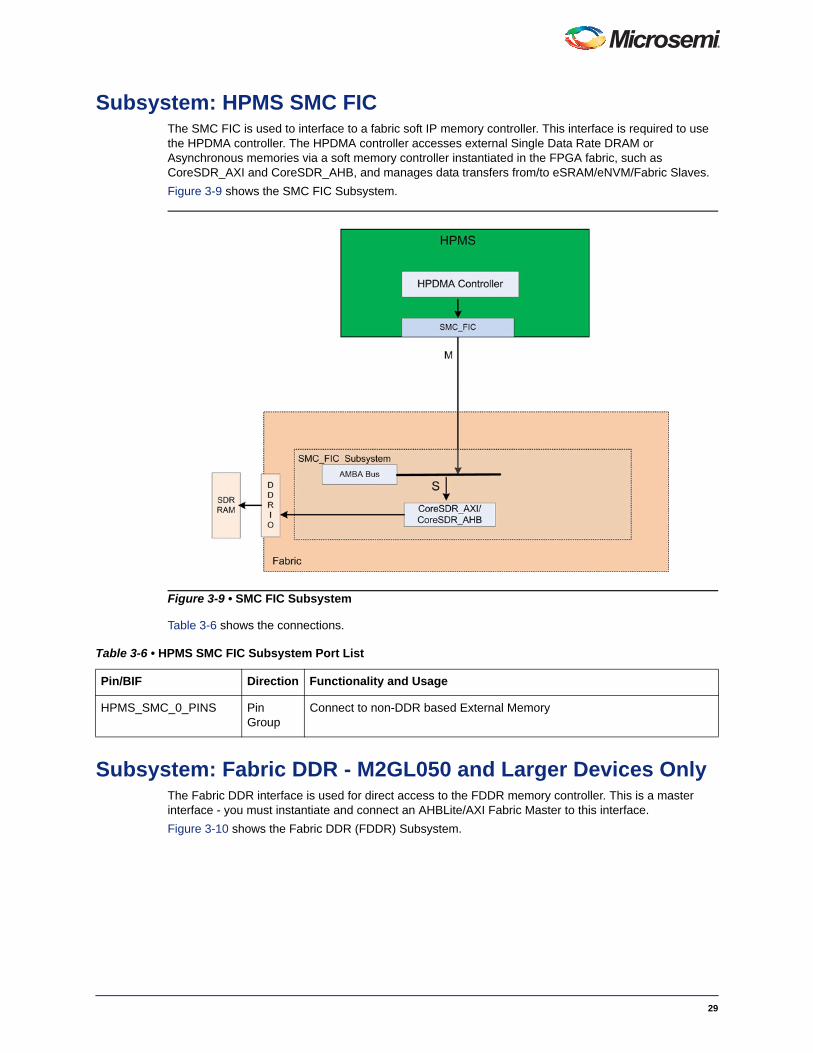
Subsystem: HPMS SMC FICThe SMC FIC is used to interface to a fabric soft IP memory controller. This interface is required to use the HPDMA controller. The HPDMA controller accesses external Single Data Rate DRAM or Asynchronous memories via a soft memory controller instantiated in the FPGA fabric, such as CoreSDR_AXI and CoreSDR_AHB, and manages data transfers from/to eSRAM/eNVM/Fabric Slaves.
Figure 3-9 shows the SMC FIC Subsystem.
Table 3-6 shows the connections.
Subsystem: Fabric DDR - M2GL050 and Larger Devices OnlyThe Fabric DDR interface is used for direct access to the FDDR memory controller. This is a master interface - you must instantiate and connect an AHBLite/AXI Fabric Master to this interface.
Figure 3-10 shows the Fabric DDR (FDDR) Subsystem.
Figure 3-9 • SMC FIC Subsystem
Table 3-6 • HPMS SMC FIC Subsystem Port List
Pin/BIF Direction Functionality and Usage
HPMS_SMC_0_PINS Pin Group
Connect to non-DDR based External Memory
29
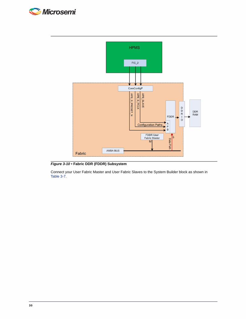
Connect your User Fabric Master and User Fabric Slaves to the System Builder block as shown in Table 3-7.
Figure 3-10 • Fabric DDR (FDDR) Subsystem
30
Table 3-7 • Fabric DDR - M2GL050 and Larger Devices
Pin/BIF Direction Functionality and Usage
System Builder Master (AHBLite /AXI) BIF Master Connect to User Fabric Master's AMBA Master BIF.
FDDR_SUBSYSTEM_PINS:FDDR_SUBSYSTEM_CLK
In Fabric DDR subsystem clock. You must provide a clock for your Fabric DDR Subsystem using one of the following options:
• Instantiate Fabric CCC in SmartDesign to generate the clock for the FDDR subsystem. The Fabric CCC will generate a clock and PLL lock signals. Connect Fabric CCC's Clock output (GL0/1/2/3) to:
• FDDR_SUBSYSTEM_CLK
• User Fabric Master's Clock Input
• User Fabric Slaves' Clock Inputs
• If you want to use the same clock frequency as one of the other subsystems (FIC_0/1 or HPMS DDR), instead of instantiating a Fabric CCC, you can get the appropriate clock and lock signals from your chosen subsystem's pins. Connect your chosen clock signal (one of FIC_0_CLK, FIC_1_CLK, or HPMS_DDR_FIC_SUBSYSTEM_CLK) to:
• FDDR_SUBSYSTEM_CLK
• User Fabric Master's Clock Input
• User Fabric Slaves' Clock Inputs
FABDDR_0_PINS:FDDR_SUBSYSTEM_PLL_LOCK
In Asserts when FDDR_SUBSYSTEM_CLK is valid. Depending on your selection of the driver of FDDR_SUBSYSTEM_CLK, connect to one of the following:
• Fabric CCC:LOCK
• System Builder block's FIC_0_LOCK, FIC_1_LOCK, or HPMS_DDR_FIC_SUBSYSTEM_LOCK
FDDR_SUBSYSTEM_PINS:FDDR_AXI_S_RMW
In Indicates whether all bytes of a 64 bit lane are valid for all beats of an AXI transfer.
0: Indicates that all bytes in all beats are valid in the burst and the controller should default to write commands
1: Indicates that some bytes are invalid and the controller should default to RMW commands
This is classed as an AXI write address channel sideband signal and is valid with the AWVALID signal.
Only used when ECC is enabled
FDDR_PADS In/Out DDR Memory Physical Interface PADs. Consult the IGLOO2 HPMS DDR User's Guide for details
31
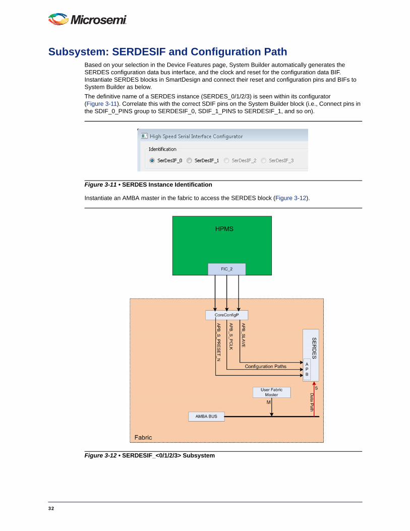
Subsystem: SERDESIF and Configuration PathBased on your selection in the Device Features page, System Builder automatically generates the SERDES configuration data bus interface, and the clock and reset for the configuration data BIF. Instantiate SERDES blocks in SmartDesign and connect their reset and configuration pins and BIFs to System Builder as below.
The definitive name of a SERDES instance (SERDES_0/1/2/3) is seen within its configurator (Figure 3-11). Correlate this with the correct SDIF pins on the System Builder block (i.e., Connect pins in the SDIF_0_PINS group to SERDESIF_0, SDIF_1_PINS to SERDESIF_1, and so on).
Instantiate an AMBA master in the fabric to access the SERDES block (Figure 3-12).
Figure 3-11 • SERDES Instance Identification
Figure 3-12 • SERDESIF_<0/1/2/3> Subsystem
32
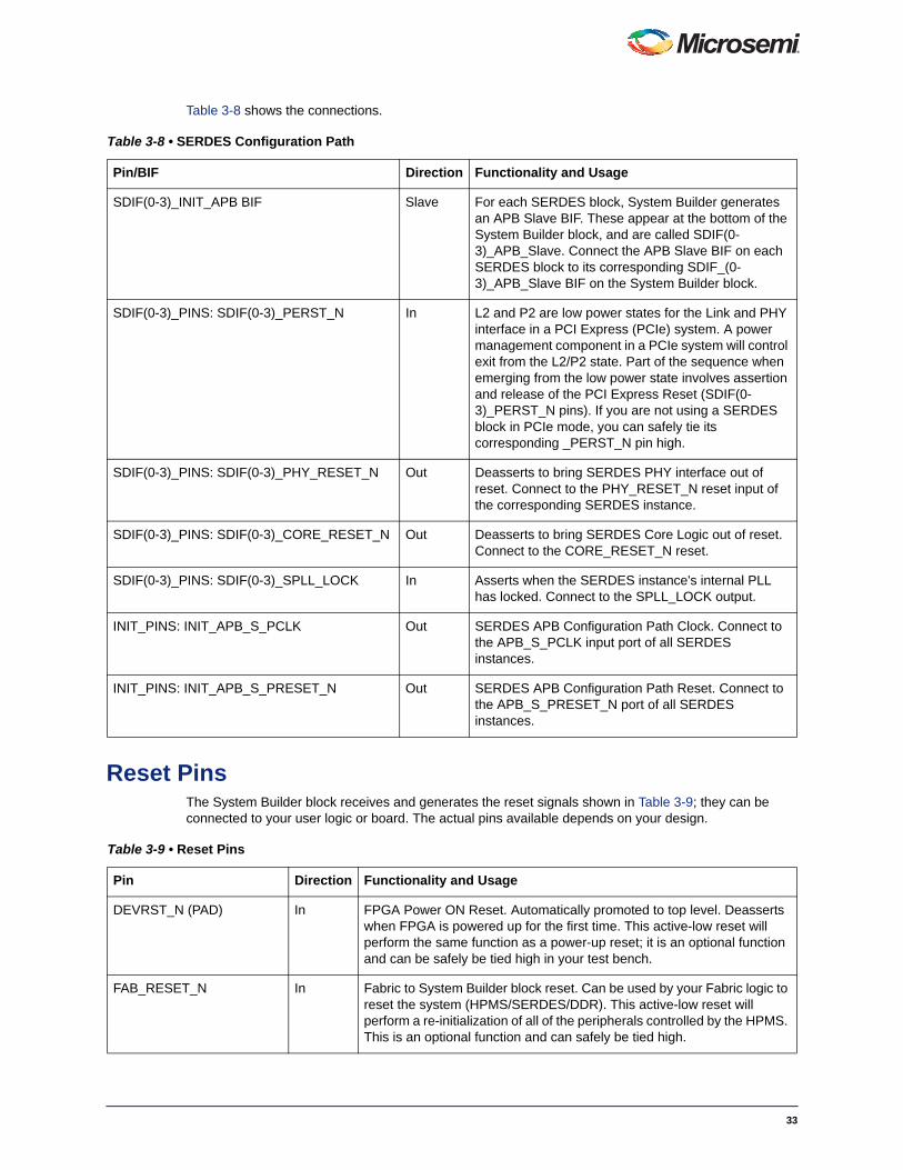
Table 3-8 shows the connections.
Reset PinsThe System Builder block receives and generates the reset signals shown in Table 3-9; they can be connected to your user logic or board. The actual pins available depends on your design.
Table 3-8 • SERDES Configuration Path
Pin/BIF Direction Functionality and Usage
SDIF(0-3)_INIT_APB BIF Slave For each SERDES block, System Builder generates an APB Slave BIF. These appear at the bottom of the System Builder block, and are called SDIF(0-3)_APB_Slave. Connect the APB Slave BIF on each SERDES block to its corresponding SDIF_(0-3)_APB_Slave BIF on the System Builder block.
SDIF(0-3)_PINS: SDIF(0-3)_PERST_N In L2 and P2 are low power states for the Link and PHY interface in a PCI Express (PCIe) system. A power management component in a PCIe system will control exit from the L2/P2 state. Part of the sequence when emerging from the low power state involves assertion and release of the PCI Express Reset (SDIF(0-3)_PERST_N pins). If you are not using a SERDES block in PCIe mode, you can safely tie its corresponding _PERST_N pin high.
SDIF(0-3)_PINS: SDIF(0-3)_PHY_RESET_N Out Deasserts to bring SERDES PHY interface out of reset. Connect to the PHY_RESET_N reset input of the corresponding SERDES instance.
SDIF(0-3)_PINS: SDIF(0-3)_CORE_RESET_N Out Deasserts to bring SERDES Core Logic out of reset. Connect to the CORE_RESET_N reset.
SDIF(0-3)_PINS: SDIF(0-3)_SPLL_LOCK In Asserts when the SERDES instance's internal PLL has locked. Connect to the SPLL_LOCK output.
INIT_PINS: INIT_APB_S_PCLK Out SERDES APB Configuration Path Clock. Connect to the APB_S_PCLK input port of all SERDES instances.
INIT_PINS: INIT_APB_S_PRESET_N Out SERDES APB Configuration Path Reset. Connect to the APB_S_PRESET_N port of all SERDES instances.
Table 3-9 • Reset Pins
Pin Direction Functionality and Usage
DEVRST_N (PAD) In FPGA Power ON Reset. Automatically promoted to top level. Deasserts when FPGA is powered up for the first time. This active-low reset will perform the same function as a power-up reset; it is an optional function and can be safely be tied high in your test bench.
FAB_RESET_N In Fabric to System Builder block reset. Can be used by your Fabric logic to reset the system (HPMS/SERDES/DDR). This active-low reset will perform a re-initialization of all of the peripherals controlled by the HPMS. This is an optional function and can safely be tied high.
33
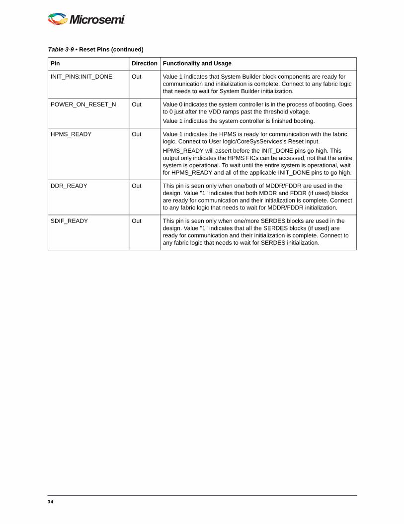
INIT_PINS:INIT_DONE Out Value 1 indicates that System Builder block components are ready for communication and initialization is complete. Connect to any fabric logic that needs to wait for System Builder initialization.
POWER_ON_RESET_N Out Value 0 indicates the system controller is in the process of booting. Goes to 0 just after the VDD ramps past the threshold voltage.
Value 1 indicates the system controller is finished booting.
HPMS_READY Out Value 1 indicates the HPMS is ready for communication with the fabric logic. Connect to User logic/CoreSysServices's Reset input.
HPMS_READY will assert before the INIT_DONE pins go high. This output only indicates the HPMS FICs can be accessed, not that the entire system is operational. To wait until the entire system is operational, wait for HPMS_READY and all of the applicable INIT_DONE pins to go high.
DDR_READY Out This pin is seen only when one/both of MDDR/FDDR are used in the design. Value "1" indicates that both MDDR and FDDR (if used) blocks are ready for communication and their initialization is complete. Connect to any fabric logic that needs to wait for MDDR/FDDR initialization.
SDIF_READY Out This pin is seen only when one/more SERDES blocks are used in the design. Value "1" indicates that all the SERDES blocks (if used) are ready for communication and their initialization is complete. Connect to any fabric logic that needs to wait for SERDES initialization.
Table 3-9 • Reset Pins (continued)
Pin Direction Functionality and Usage
34
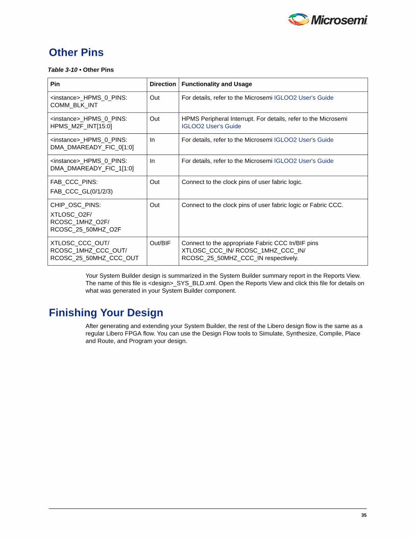
Other Pins
Your System Builder design is summarized in the System Builder summary report in the Reports View. The name of this file is <design>_SYS_BLD.xml. Open the Reports View and click this file for details on what was generated in your System Builder component.
Finishing Your DesignAfter generating and extending your System Builder, the rest of the Libero design flow is the same as a regular Libero FPGA flow. You can use the Design Flow tools to Simulate, Synthesize, Compile, Place and Route, and Program your design.
Table 3-10 • Other Pins
Pin Direction Functionality and Usage
<instance>_HPMS_0_PINS: COMM_BLK_INT
Out For details, refer to the Microsemi IGLOO2 User's Guide
<instance>_HPMS_0_PINS: HPMS_M2F_INT[15:0]
Out HPMS Peripheral Interrupt. For details, refer to the Microsemi IGLOO2 User's Guide
<instance>_HPMS_0_PINS: DMA_DMAREADY_FIC_0[1:0]
In For details, refer to the Microsemi IGLOO2 User's Guide
<instance>_HPMS_0_PINS: DMA_DMAREADY_FIC_1[1:0]
In For details, refer to the Microsemi IGLOO2 User's Guide
FAB_CCC_PINS:
FAB_CCC_GL(0/1/2/3)
Out Connect to the clock pins of user fabric logic.
CHIP_OSC_PINS:
XTLOSC_O2F/RCOSC_1MHZ_O2F/RCOSC_25_50MHZ_O2F
Out Connect to the clock pins of user fabric logic or Fabric CCC.
XTLOSC_CCC_OUT/ RCOSC_1MHZ_CCC_OUT/ RCOSC_25_50MHZ_CCC_OUT
Out/BIF Connect to the appropriate Fabric CCC In/BIF pins XTLOSC_CCC_IN/ RCOSC_1MHZ_CCC_IN/ RCOSC_25_50MHZ_CCC_IN respectively.
35
A – Product Support
Microsemi SoC Products Group backs its products with various support services, including Customer Service, Customer Technical Support Center, a website, electronic mail, and worldwide sales offices. This appendix contains information about contacting Microsemi SoC Products Group and using these support services.
Customer ServiceContact Customer Service for non-technical product support, such as product pricing, product upgrades, update information, order status, and authorization.
From North America, call 800.262.1060From the rest of the world, call 650.318.4460Fax, from anywhere in the world, 408.643.6913
Customer Technical Support CenterMicrosemi SoC Products Group staffs its Customer Technical Support Center with highly skilled engineers who can help answer your hardware, software, and design questions about Microsemi SoC Products. The Customer Technical Support Center spends a great deal of time creating application notes, answers to common design cycle questions, documentation of known issues, and various FAQs. So, before you contact us, please visit our online resources. It is very likely we have already answered your questions.
Technical SupportVisit the Customer Support website (www.microsemi.com/soc/support/search/default.aspx) for more information and support. Many answers available on the searchable web resource include diagrams, illustrations, and links to other resources on the website.
WebsiteYou can browse a variety of technical and non-technical information on the SoC home page, at www.microsemi.com/soc.
Contacting the Customer Technical Support CenterHighly skilled engineers staff the Technical Support Center. The Technical Support Center can be contacted by email or through the Microsemi SoC Products Group website.
EmailYou can communicate your technical questions to our email address and receive answers back by email, fax, or phone. Also, if you have design problems, you can email your design files to receive assistance. We constantly monitor the email account throughout the day. When sending your request to us, please be sure to include your full name, company name, and your contact information for efficient processing of your request.
The technical support email address is [email protected].
36
MOWSaFa
Microsemi Corporation (NASDAQ: MSCC) offers a comprehensive portfolio of semiconductorsolutions for: aerospace, defense and security; enterprise and communications; and industrialand alternative energy markets. Products include high-performance, high-reliability analogand RF devices, mixed signal and RF integrated circuits, customizable SoCs, FPGAs, andcomplete subsystems. Microsemi is headquartered in Aliso Viejo, Calif. Learn more atwww.microsemi.com.
icrosemi Corporate Headquarters
My CasesMicrosemi SoC Products Group customers may submit and track technical cases online by going to My Cases.
Outside the U.S.Customers needing assistance outside the US time zones can either contact technical support via email ([email protected]) or contact a local sales office. Sales office listings can be found at www.microsemi.com/soc/company/contact/default.aspx.
ITAR Technical SupportFor technical support on RH and RT FPGAs that are regulated by International Traffic in Arms Regulations (ITAR), contact us via [email protected]. Alternatively, within My Cases, select Yes in the ITAR drop-down list. For a complete list of ITAR-regulated Microsemi FPGAs, visit the ITAR web page.
5-02-00488-4/08.14
© 2014 Microsemi Corporation. All rights reserved. Microsemi and the Microsemi logo are trademarks ofMicrosemi Corporation. All other trademarks and service marks are the property of their respective owners.
ne Enterprise, Aliso Viejo CA 92656 USAithin the USA: +1 (949) 380-6100les: +1 (949) 380-6136x: +1 (949) 215-4996
Recommended