Page 259
IC Layout Design of Decoders Using DSCH and Microwind Shaik Fazia Kausar
MTech,
Dr.K.V.Subba Reddy Institute of Technology.
T.Vijay Kumar, M.Tech
Associate Professor,
Dr.K.V.Subba Reddy Institute of Technology.
Abstract:
Low power issues have become an important factor in
modern VLSI design .This paper discusses the design
of an Integrated Circuit (IC) layout for a decoder. The
decoders are designed by using Schematic and Layout
editor tools DSCH3.5 and Microwind3.5. In order to
produce the schematic and layout, the basic knowledge
of fabrication process and IC design rules are
expounded. The complete layout of the decoder was
designed based on its schematic circuit, which consists
of NOT gates, 2-input NAND gates, 3-input NAND
gates, 4-input NAND gates, 2- input AND gates and 3-
input AND gates. The layout had undergone Design
Rule Check (DRC) set by the DSCH3.5 to check for
any design rule error. Both layout and schematic
circuit of the decoder were simulated through
DSCH3.5 and Microwind3.5 to ensure they were
identical with 65nm. DSCH is used as simulator to
carry out the simulation work and verify the validity of
the function. The simulation output indicated that
results of the layout and schematic circuit for decoder
were essentially identical and matches the theoretical
results.
Index Terms:Decoder, schematic circuit, IC layout,
DSCH3.5 and Microwind3.5, NAND gates, AND
gates and simulation output.
I. INTRODUCTION:
Electronic devices have been widely used in many
different fields and the size of these devices has been
gradually reduced. An example of this is the mobile
phone which is made smaller to enhance user‟s
mobility and usage time. These are the contribution of
integrated circuit (IC) technology. With this
technology, the modern devices have been reduced to
convenient sizes.
Besides that, mass production of IC has lowered the
cost of production and made most electronic devices
affordable. Today, an IC is smaller than a coin and can
hold millions of transistors. Hence, further research in
the design of IC is important to enhance the production
of a more efficient and viable IC. The main objective
of this paper is to design an IC layout of a 7-segments
decoder by Microwind3.5 and DSCH3.5. The tools are
Schematic and Layout editor tools that provides
service in handling IC layout, schematicdrawing,
textual hardware description language, and other
features [1]. By using this software‟s, a micrometer
sized IC can be easily designed due to the availability
of various features that can be used to design and
check the IC layout. Moreover, DSCH3.5 and
Microwind3.5 also allows the schematic and layout
design to be done in a systematic and efficient manner,
thus saving time and reducing the production cost of
the IC chip. There are different technologies to
construct integrated circuits such as bipolar integrated
technology, NMOS technology and CMOS
technology. In this project, CMOS technology is used.
The main reason in using CMOS technology is due to
its scalable high noise immunity and low power
consumption. Basically, CMOS technology uses both
NMOS and PMOS, which means only either one of
both types of transistors will be ON at a time during
the operation. Thus, CMOS IC consumes less power as
power is used only when the NMOS and PMOS
transistors are switching between on and off states [2].
II. LITERATURE REVIEW:
In present scenario, power reduction is a major issue in
the technology world. The low power design is major
issue in high performance digital system, such as
microprocessors, digital signal processors (DSPs),7-
Segments display and other applications.

Page 260
The chip density and higher operating speed leads to
the design of very complex chips with high clock
frequencies. So designing of low power VLSI circuits
is a technological need in these due to the high demand
for portable consumer electronics products [2]. The
development of electronic technology was started with
the use of vacuum tube as active component in
electronic series before semiconductor transistor
replaces it. The development of microelectronic
technology especially for those of mono-litical is able
to produce interfaced circuit by combining all active
and passive components in one chip [3]. High speed
serializer/deserializers (SerDes) are now more and
more widely used in communication systems for serial
interconnections [4]. Decoders are used whenever an
output or a group of outputs is to activated only on the
occurrence of specific combination of input levels.
These input levels are often provided by the outputs of
a counter or register. When the decoder inputs come
from a counter that is being continually pulsed, the
decoder outputs will be activated sequentially, and
they can be used as timing or sequencing the signals to
turn devices ON or OFF at specific times. Decoders
are widely used in memory systems of computers,
where they respond to the address code input from the
central processor to activate the memory storage
location specified by the address code [1].
A. 7-Segments Decoder
A 7-segments decoder is able to convert the logic
states of inputs into seven bits of outputs and displays
in 7-segments display. It is used widely in devices
where its main function is to display numbers from a
digital circuitry. Examples of these devices includes
calculators, displays in elevator, digital timers, digital
clocks and etc. There are many types of decoders such
as 2-4 decoder, 3- 8 decoder and 4-16 decoder. Since
there are ten decimal numerals (0–9) to be displayed in
the 7-segments display, a 4-16 decoder was used.The
structure of a 7-segments display is shown in Fig. 1. It
is used to display decimal numerals in seven segments
and each segment is represented by an alphabet „a‟ to
„g‟.
By setting the required segments to be turned on, the
desired decimal numeral can be displayed on the 7-
segments display. The logic diagram of 7-segments
decoder is shown in Fig. 2.
Figure 1. Structure of a 7-segments display
Figure 2. The logic diagram of a 7-segments
decoder [3]
Page 261
B. IC Design rules:
IC layouts are built from three basic components
which are the transistors, wires and vias. During the
design of the layouts, the design rule has to be
considered. Design rules govern the layout of
individual components and the interaction between
those components. When designing an IC, designers
tend to make the components as small as possible
enabling implementation of as many functions as
possible onto a single chip. However, since the
transistors and wires are extremely small, errors may
happen during the fabrication process. Hence, design
rules are created and formulated to minimise problems
during fabrication process and helps to increase the
yield of correct chips to a suitable level. Therefore, it
is important to adhere to the design rules during layout
design.
C. Physical Verification of Design [1], [4]
Physical verification is a process where an IC layout
design will be checked via DSCH3.5 and
Microwind3.5 EDA tools to ensure it meets design
criteria and rules. The verification process used in this
project involves DRC (Design Rule Check) and ERC
(Electrical Rule Check). These are important
procedures in IC layout design and cannot be treated
lightly.
i) Design Rule Check (DRC) DRC is a verification
process that determines whether the physical layout
of a chip design satisfies the Design Rules or not. It
ensures that all the polygons and layers meet the
manufacturing process rules that defines the limits
of a manufacturing design such as the width and
space rules. DRC is the first level of verification
once the layout is ready. In this verification stage,
the connectivity and guidelines rules will be
checked as well. DRC will not only check the
designs that are created by the designers, but also
the design placed within the context in which it is
going to be used. Therefore, the possibility of errors
in the design will be greatly reduced and a high
overall yield and reliability of design will be
achieved.
ii) Electrical Rules Check (ERC) ERC is usually
used to check the errors in connectivity or device
connection. It is an optional choice of checking
and seldom used as an independent verification
step. ERC is usually used to check for any
unconnected, partly connected or redundant
devices. Also, it will check for any disabled
transistors, floating nodes and short circuits. ERC
is very useful in accelerating debugging problems
such as short circuits as can speed up the design
process.
III. Decoder IC basic Elements:
In this project, an IC layout of a decoder that displays
the decimal numeral in 7-segments display was
designed. It consists of NOT gates, 2-input NAND
gates, 3-input NAND gates, 4-input NAND gates, 2-
input AND gates and 3-input AND gates. The
schematic circuits and layouts of all these gates were
drawn and simulated using DSCH3.5 and
Microwind3.5.
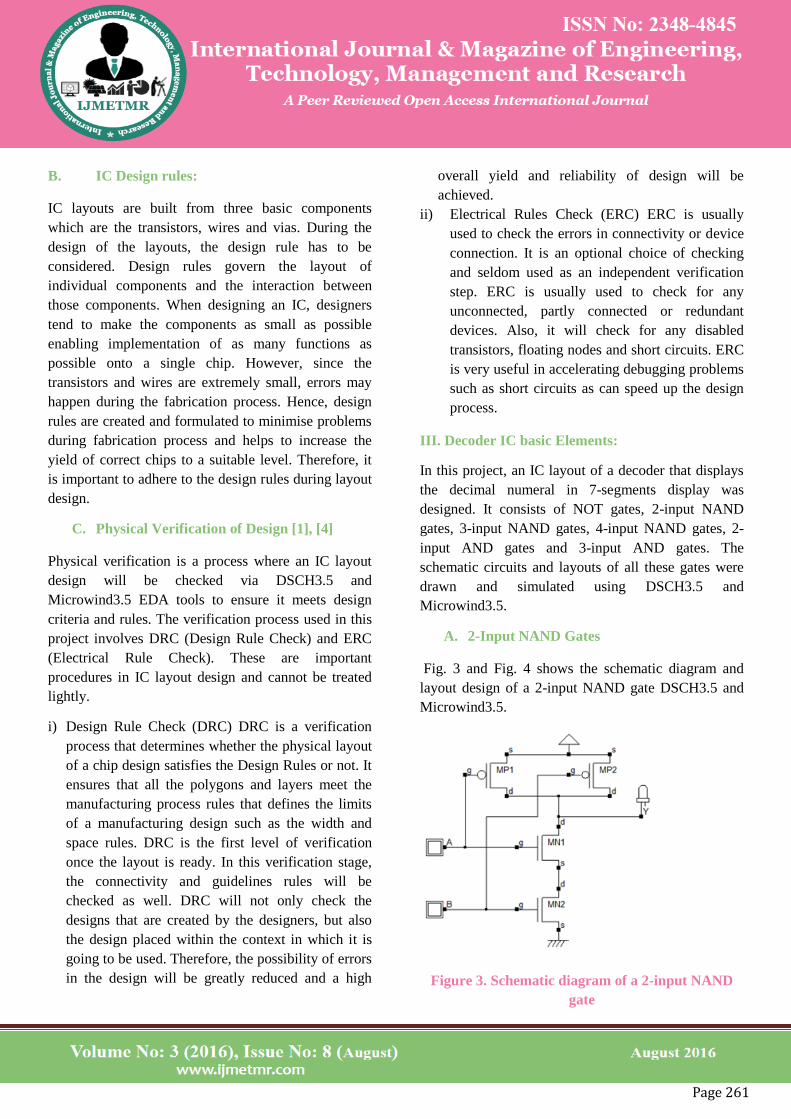
A. 2-Input NAND Gates
Fig. 3 and Fig. 4 shows the schematic diagram and
layout design of a 2-input NAND gate DSCH3.5 and
Microwind3.5.
Figure 3. Schematic diagram of a 2-input NAND
gate
Page 262
Figure 4. Layout design of 2-input NAND gate
B. 3-Input NAND Gates
Fig. 5 and Fig. 6 show the schematic diagram and
layout of a 3-input NAND gate.
Figure 5. Schematic diagram of a 3-input NAND
gate
Figure 6. Layout design of a 3-input NAND gate
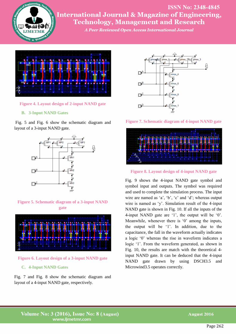
C. 4-Input NAND Gates
Fig. 7 and Fig. 8 show the schematic diagram and
layout of a 4-input NAND gate, respectively.
Figure 7. Schematic diagram of 4-input NAND gate
Figure 8. Layout design of 4-input NAND gate
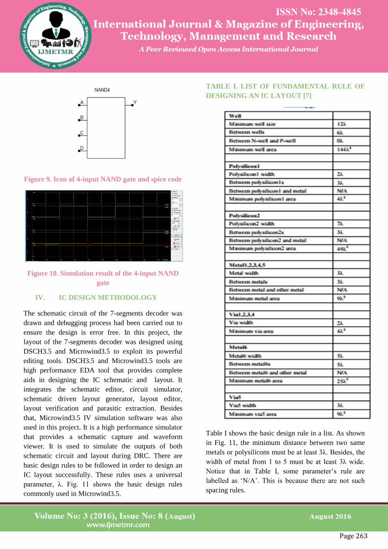
Fig. 9 shows the 4-input NAND gate symbol and
symbol input and outputs. The symbol was required
and used to complete the simulation process. The input
wire are named as „a‟, „b‟, „c‟ and „d‟; whereas output
wire is named as „y‟. Simulation result of the 4-input
NAND gate is shown in Fig. 10. If all the inputs of the
4-input NAND gate are „1‟, the output will be „0‟.
Meanwhile, whenever there is „0‟ among the inputs,
the output will be „1‟. In addition, due to the
capacitance, the fall in the waveform actually indicates
a logic „0‟ whereas the rise in waveform indicates a
logic „1‟. From the waveform generated, as shown in
Fig. 10, the results are match with the theoretical 4-
input NAND gate. It can be deduced that the 4-input
NAND gate drawn by using DSCH3.5 and
Microwind3.5 operates correctly.
Page 263
Figure 9. Icon of 4-input NAND gate and spice code
Figure 10. Simulation result of the 4-input NAND
gate
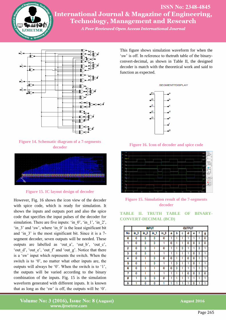
IV. IC DESIGN METHODOLOGY
The schematic circuit of the 7-segments decoder was
drawn and debugging process had been carried out to
ensure the design is error free. In this project, the
layout of the 7-segments decoder was designed using
DSCH3.5 and Microwind3.5 to exploit its powerful
editing tools. DSCH3.5 and Microwind3.5 tools are
high performance EDA tool that provides complete
aids in designing the IC schematic and layout. It
integrates the schematic editor, circuit simulator,
schematic driven layout generator, layout editor,
layout verification and parasitic extraction. Besides
that, Microwind3.5 IV simulation software was also
used in this project. It is a high performance simulator
that provides a schematic capture and waveform
viewer. It is used to simulate the outputs of both
schematic circuit and layout during DRC. There are
basic design rules to be followed in order to design an
IC layout successfully. These rules uses a universal
parameter, λ. Fig. 11 shows the basic design rules
commonly used in Microwind3.5.
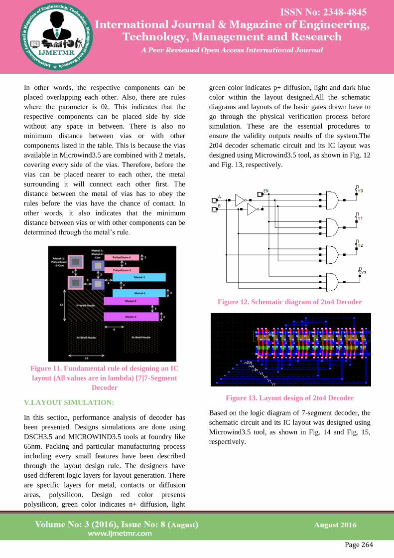
TABLE I. LIST OF FUNDAMENTAL RULE OF
DESIGNING AN IC LAYOUT [7]
Table I shows the basic design rule in a list. As shown
in Fig. 11, the minimum distance between two same
metals or polysilicons must be at least 3λ. Besides, the
width of metal from 1 to 5 must be at least 3λ wide.
Notice that in Table I, some parameter‟s rule are
labelled as „N/A‟. This is because there are not such
spacing rules.
Page 264
In other words, the respective components can be
placed overlapping each other. Also, there are rules
where the parameter is 0λ. This indicates that the
respective components can be placed side by side
without any space in between. There is also no
minimum distance between vias or with other
components listed in the table. This is because the vias
available in Microwind3.5 are combined with 2 metals,
covering every side of the vias. Therefore, before the
vias can be placed nearer to each other, the metal
surrounding it will connect each other first. The
distance between the metal of vias has to obey the
rules before the vias have the chance of contact. In
other words, it also indicates that the minimum
distance between vias or with other components can be
determined through the metal‟s rule.
Figure 11. Fundamental rule of designing an IC
layout (All values are in lambda) [7]7-Segment
Decoder
V.LAYOUT SIMULATION:
In this section, performance analysis of decoder has
been presented. Designs simulations are done using
DSCH3.5 and MICROWIND3.5 tools at foundry like
65nm. Packing and particular manufacturing process
including every small features have been described
through the layout design rule. The designers have
used different logic layers for layout generation. There
are specific layers for metal, contacts or diffusion
areas, polysilicon. Design red color presents
polysilicon, green color indicates n+ diffusion, light
green color indicates p+ diffusion, light and dark blue
color within the layout designed.All the schematic
diagrams and layouts of the basic gates drawn have to
go through the physical verification process before
simulation. These are the essential procedures to
ensure the validity outputs results of the system.The
2t04 decoder schematic circuit and its IC layout was
designed using Microwind3.5 tool, as shown in Fig. 12
and Fig. 13, respectively.
Figure 12. Schematic diagram of 2to4 Decoder
Figure 13. Layout design of 2to4 Decoder
Based on the logic diagram of 7-segment decoder, the
schematic circuit and its IC layout was designed using
Microwind3.5 tool, as shown in Fig. 14 and Fig. 15,
respectively.
Page 265
Figure 14. Schematic diagram of a 7-segments
decoder
Figure 15. IC layout design of decoder
However, Fig. 16 shows the icon view of the decoder
with spice code, which is ready for simulation. It
shows the inputs and outputs port and also the spice
code that specifies the input pulses of the decoder for
simulation. There are five inputs: „in_0‟, „in_1‟, „in_2‟,
„in_3‟ and „sw‟, where „in_0‟ is the least significant bit
and „in_3‟ is the most significant bit. Since it is a 7-
segment decoder, seven outputs will be needed. These
outputs are labelled as „out_a‟, „out_b‟, „out_c‟,
„out_d‟, „out_e‟, „out_f‟ and „out_g‟. Notice that there
is a „sw‟ input which represents the switch. When the
switch is to „0‟, no matter what other inputs are, the
outputs will always be „0‟. When the switch is to „1‟,
the outputs will be varied according to the binary
combination of the inputs. Fig. 15 is the simulation
waveform generated with different inputs. It is known
that as long as the „sw‟ is off, the outputs will be „0‟.
This figure shows simulation waveform for when the
„sw‟ is off. In reference to thetruth table of the binary-
convert-decimal, as shown in Table II, the designed
decoder is match with the theoretical work and said to
function as expected.
Figure 16. Icon of decoder and spice code
Figure 15. Simulation result of the 7-segments
decoder
TABLE II. TRUTH TABLE OF BINARY-
CONVERT-DECIMAL (BCD)

Page 266
VI CONCLUSION:
The design and analysis of decoder and its 7-segment
display has been presented. Designs simulations are
done using DSCH3.5 and MICROWIND3.5 tools at
foundry like 65nm. 7-segments decoder IC is to
display the numbers in 7 segments. It converts the
binary input to 7 bits according to the input. The IC
layout of the decoder is designed and successfully
proves that the output waveforms generated matches
the theoretical decoder. In addition, DSCH3.5 and
Microwind3.5 tools are user friendly software‟s to be
used in designing a layout of 7-segments decoder. It is
expected that the software‟sare able to cope with more
complex digital IC design with its suite of verification
and design tools.
REFERENCES:
[1] About DSCH3.5 and Microwind3.5(May 2014).
[Online]. Available: http://www.microwind.net
[2] A. Anand Kumar, “Fundamentals of Digital
Circuits” Second Edition, Prentice Hall of India, pp.
337-340, 2006.
[3] Ranjan Kumar Singh, Rakesh Jain,
“Implementation And Analysis of Power Reduction In
2 to 4 Decoder Design Using Adiabatic Logic”,
International Journal of Research in Engineering and
Technology (IJRET) eISSN: 2319-1163, Volume-03
Issue-07, pp. 172-175, July 2014
[4] R. J. Baker, CMOS: Circuit Design, Layout, and
Simulation, John Wiley & Sons, 2010, pp. 6-12.
[5] M. M. Forrest, Understanding Digital Computers,
Radio Shack, 1987.
[6] S. H. Teen and S. Y. Lee, “CMOS IC layout
design: 7-segments counter,” Lecture Notes on
Photonics and Optoelectronics, vol. 1, no. 2, pp. 52-55,
December 2013.
[7] A. P. Douglas and E. Kamran, Basic VLSI Design,
3rd ed., Prentice Hall, 1994, pp. 72-76.
Recommended