Hybrid RF-Digital Feed-Forward Filter for
High-Order Frequency Agile Filtering
by
Mark Wyville, B.Eng., M.A.Sc.
A thesis submitted to the Faculty of Graduate and Postdoctoral Affairs
in partial fulfillment of the requirements for the degree of
Doctor of Philosophy
in Electrical Engineering
Ottawa-Carleton Institute for Electrical and Computer Engineering
Department of Electronics
Carleton University
Ottawa, Ontario
June, 2011
Copyright ©2011, Mark Wyville

1*1 Library and Archives Canada
Published Heritage Branch
395 Wellington Street OttawaONK1A0N4 Canada
Bibliotheque et Archives Canada
Direction du Patrimoine de I'edition
395, rue Wellington OttawaONK1A0N4 Canada
Your file Votre reference ISBN: 978-0-494-83234-9 Our file Notre r6f6rence ISBN: 978-0-494-83234-9
NOTICE: AVIS:
The author has granted a nonexclusive license allowing Library and Archives Canada to reproduce, publish, archive, preserve, conserve, communicate to the public by telecommunication or on the Internet, loan, distribute and sell theses worldwide, for commercial or noncommercial purposes, in microform, paper, electronic and/or any other formats.
L'auteur a accorde une licence non exclusive permettant a la Bibliotheque et Archives Canada de reproduire, publier, archiver, sauvegarder, conserver, transmettre au public par telecommunication ou par I'lnternet, preter, distribuer et vendre des theses partout dans le monde, a des fins commerciales ou autres, sur support microforme, papier, electronique et/ou autres formats.
The author retains copyright ownership and moral rights in this thesis. Neither the thesis nor substantial extracts from it may be printed or otherwise reproduced without the author's permission.
L'auteur conserve la propriete du droit d'auteur et des droits moraux qui protege cette these. Ni la these ni des extraits substantiels de celle-ci ne doivent etre imprimes ou autrement reproduits sans son autorisation.
In compliance with the Canadian Privacy Act some supporting forms may have been removed from this thesis.
Conformement a la loi canadienne sur la protection de la vie privee, quelques formulaires secondaires ont ete enleves de cette these.
While these forms may be included in the document page count, their removal does not represent any loss of content from the thesis.
Bien que ces formulaires aient inclus dans la pagination, il n'y aura aucun contenu manquant.
I + l
Canada

Abstract
Wireless network operators, spectrum managers and wireless infrastructure vendors have
generated demand for frequency agile RF filters. The current state of the art frequency
agile RF filters are limited to low filter order.
This thesis introduces a frequency agile RF filter that is fundamentally different from the
current state of the art. Digital and RF systems are combined in a feed-forward
architecture. This architecture provides a frequency response with multiple tunable
transfer function zeros. This feed-forward architecture is called the hybrid RF-DSP feed
forward filter.
The digital subsystem is placed in one of the feed-forward paths, and includes a digital
filter. The digital filter permits the system to have a high filter order. The digital system is
bookended with frequency down and up conversion stages to permit the digital filter to be
used at any RF frequency. The second feed-forward path consists of an RF system, and in
the simplest case is just a transmission line. This path provides a high dynamic range
route through the filter, specifically for passband signals.
Noise and attenuation analyses are performed that incorporate the non-linear effects of
the digital components into conventional RF performance metrics. The noise analysis
demonstrates the potential for the filter to exhibit less than 1 dB of noise figure.
RF measurements are used to demonstrate proper operation of a hardware prototype. The
prototype is targeted towards the RF front-end of a receiver with a dynamic interference
environment at its input. Measurements demonstrate interferer suppression for operation
at several bands between 800 and 1800 MHz. The group delay mismatch between the
feed-forward paths is reduced with a delay line to achieve between 32 to 24 dB of
ii

attenuation for interferers with bandwidths from 1 to 8 MHz. The largest digital filter
used within the prototype has 64 complex taps, thereby providing the hybrid RF-DSP FF
filter with 64 tunable transfer function zeros.
The hybrid RF-DSP feed-forward filter represents a fundamental change to frequency
agile RF filter design. This fundamental change is based on harnessing the ever
increasing processing power of DSP instead of the more traditional approach of
incrementally improving the quality factor of tunable resonators.
i i i

Acknowledgements
I am grateful to my academic supervisor, Jim Wight, who many years ago advised me to
pursue graduate studies on what I thought was my last day at university. I would like to
thank him for all of the support he has made available in a number of ways.
Also from Carleton University I would like to express my gratitude towards Nagui
Mikhail, the department's 'hidden hero' for all of the time and advice he provided to help
me with a diverse range of issues.
At Ericsson I would like to acknowledge Russell Smiley for his leadership and for
volunteering for the workload associated with overseeing a graduate student outside of
the university.
At home I would like to thank my wife for her patience and loving support.
iv

Table of Contents
Abstract ii Acknowledgements iv Table of Contents v List of Figures viii List of Abbreviations xii 1 Introduction 1
1.1 Motivation 1 1.2 Current State of the Art 4 1.3 Thesis Objectives 6 1.4 The Hybrid RF-DSP FF Filter 6
1.4.1 Overview of Main Results 8 1.5 List of Contributions 9 1.6 Thesis Organization 10
2 Literature Review 12 2.1 Reconfigurable BPF's 12
2.1.1 MEMS 15 2.1.2 Varactor Diodes 19 2.1.3 PIN Diodes 21 2.1.4 Ferroelectric 22 2.1.5 Ferrite 23
2.2 Reconfigurable Multiple Stopband Filters 25 2.2.1 FF Amplifier Linearization 25 2.2.2 Interferer Attenuation in Receiver 28 2.2.3 Feedforward Duplexer Isolation Improvement 30
2.3 Summary of Literature Review 36 3 System Description 37
3.1 System Architecture 37 3.1.1 Digital Filter 40 3.1.2 Direct Up and Down Conversion 42 3.1.3 Tunable BSF 43
3.2 Applications 45 3.2.1 Applications in the Receive Chain 45 3.2.2 Application in the Transmit Chain 48 3.2.3 Application for Duplexer Isolation Improvement 50
3.3 Summary of System Description 51 4 Theoretical Analyses 52
4.1 Noise Analysis 52 4.1.1 Noise Model 53 4.1.2 Noise of RF and Analog Components 55 4.1.3 Noise of Digital Components 57 4.1.4 Noise Expression Discussion 66
v

4.1.5 Simulation for Verification ofFDIG 76 4.2 Feedforward Attenuation Analysis 80
4.2.1 Filter Tap Quantization 81 4.2.2 Group Delay Mismatch 82 4.2.3 Number of Filter Taps 88
4.3 Analyses Summary 88 5 Algorithm Development 90
5.1 Filter Optimization Strategy 90 5.2 Hybrid RF-DSP FF Filter Model 93
5.2.1 Model Manipulation for Adaptive Whitening 94 5.2.2 Block LMS Algorithm 99 5.2.3 Verification with Maximum Precision Simulation 103
5.3 Estimating h23[n] 108 5.3.1 Effect of Errors in h23>est[n] 109
5.4 Algorithm for Tunable BSF Control 116 5.5 Finite Precision Effects 117 5.6 Algorithm Development Summary 121
6 Hardware Prototype 123 6.1 Description of Components 123 6.2 Bottom FF Path Characterization 126
6.2.1 Magnitude Response itfl-ADCl Chain 127 6.2.2 Primary ADC's 128 6.2.3 Noise Factor of RF\ Chain 130 6.2.4 Magnitude Response DAC-RF2 Chain 131 6.2.5 Noise Factor of RF2 Chain 132 6.2.6 Primary DAC's 133 6.2.7 Group Delay 135 6.2.8 LO Phase Noise 137 6.2.9 Summary of Bottom FF Path Characterization 138
6.3 Algorithm Verification 140 6.3.1 Verification of BSF Algorithm 140 6.3.2 Verification of h23,est[n\ Estimation Algorithm 142 6.3.3 Verification of Main Algorithm 147
6.4 Hardware Prototype Summary 149 7 Hardware Prototype Performance 150
7.1 Measurement Setup 150 7.2 Narrowband Inputs 151
7.2.1 Frequency Agility 151 7.2.2 Dynamically Changing Inputs 154 7.2.3 Near Band Attenuation 156
7.3 Wideband Inputs 158 7.3.1 Vary Number of Taps 161 7.3.2 Vary Algorithm Block Size 162 7.3.3 Vary Group Delay 164
7.4 Noise Analysis Verification 165 7.4.1 Expected Output Noise 166
vi

7.4.2 Measured Versus Expected Output Noise 166 7.5 Prototype Performance Summary 171
8 Conclusions and Discussions 173 8.1 First Order Approximations 173
8.1.1 Dynamic Range 173 8.1.2 Group Delay 175
8.2 Improvements and Future Work 179 8.2.1 Equalizing ADC's and DAC's 179 8.2.2 Notch Constraints on Digital Filter 181 8.2.3 Digital IIR stage 184 8.2.4 Negative Group Delay 185
8.3 Discussion Summary 187 8.4 Conclusion 187
8.4.1 List of Contributions 187 References 189 Appendix A - Filter Tap Quantization 193
vn
List of Figures Figure 1.4.1 - System-level schematic of hybrid FF filter 7 Figure 2.1.1- Insertion loss of 0.1 dB ripple Chebyshev LPF with unity cut-off frequency
13 Figure 2.1.2 - Required Q for 1 dB insertion loss of 0.1 dB ripple Chebyshev BPF 14 Figure 2.1.3 - Required Q for 2 dB insertion loss with 1 dB ripple Chebyshev BPF 15 Figure 2.1.4 - Varactor configurations for improved linearity a) Anti-series b) Anti-series
with anti-parallel in bias 19 Figure 2.1.5 - Ferrite sphere BPF 24 Figure 2.2.1 - FF amplifier linearization a) typical linearizer b) extra path in error
cancellation loop 26 Figure 2.2.2 - DSP path in signal cancellation loop [25] 27 Figure 2.2.3 - Blocker attenuation in receiver prior to mixer [26] 28 Figure 2.2.4 - FF attenuation to receiver [27] 31 Figure 2.2.5 - Frequency agile BSF schematic [28] 33 Figure 2.2.6 - Auxiliary transmitter attenuation [29] 34 Figure 2.2.7 - Double loop attenuation [30] 35 Figure 3.1.1 - System-level schematic of hybrid RF-DSP FF filter 38 Figure 3.1.2 - Component-level schematic of hybrid RF-DSP FF filter 40 Figure 3.1.3 - DSP filtering configuration 41 Figure 3.1.4 - R L C BSF combined digital and RF 44 Figure 3.1.5 - FF BSF combined digital and RF 44 Figure 3.2.1 -Pre-LNA interference filtering application 46 Figure 3.2.2 - PSD at different locations around filter 47 Figure 3.2.3 - System-level schematic of hybrid FF filter 48 Figure 3.2.4 -Post-PA IMD and spur filtering application 49 Figure 3.2.5 - Improved isolation application 50 Figure 4.1.1 - Setup for noise analysis 53 Figure 4.1.2 - Block diagram for noise analysis 54 Figure 4.1.3 - Simplified block diagram for noise analysis 54 Figure 4.1.4 - Direct-conversion implementation of DEMOD and MOD blocks 55 Figure 4.1.5 - Direct-form FIR filter with 2 complex taps showing quantization noise.. 61 Figure 4.1.6 - Complex multiplier implementation with three multipliers 61 Figure 4.1.7 - Digital BSF compensation with noise sources 64 Figure 4.1.8 - Details of'Real Mult' in Fig. 4.1.7 64 Figure 4.1.9 -Noise factor contribution from first two terms in (4.1.30) for various
couplers 69 Figure 4.1.10 - Simulink model for digital noise analysis 77 Figure 4.1.11 -Details of'Digital filter stuff block from Fig. 4.1.10 77 Table 4.1 -Noise simulation results for varying digital resources 80 Figure 4.2.1 - Linear discrete-time model of hybrid RF-DSP FF filter 83 Figure 4.2.2 -Equivalent model to Fig. 4.2.1 when digital filter is in steady-state 83 Figure 4.2.3 -Compressed block diagram a) version 1 b) version 2 84 Figure 5.1.1 -ARMA process and whitening filter 91 Figure 5.1.2 - AR process generated by passing white noise through an all-pole filter .. 92
vm
Figure 5.2.1 - Block diagram of hybrid RF-DSP FF filter 94 Figure 5.2.2 - Linear discrete-time model of hybrid RF-DSP FF filter 94 Figure 5.2.3 - Standard linear adaptive filter 95 Figure 5.2.4 - Equivalent model to Fig. 5.2.2 95 Figure 5.2.5 - Equivalent model to Fig. 5.2.4 when digital filter coefficients are fixed.. 96 Figure 5.2.6 - Generation of ues,\n\ for gradient estimation 97 Figure 5.2.7 -Realizations of cascade of HA{z) and77B(z) 98 Figure 5.2.8 - Simulink model of hybrid RF-DSP FF filter with hn est[n] known a priori
'. 104 Figure 5.2.9 - PSD at input and output of hybrid RF-DSP FF filter 106 Figure 5.2.10 - Magnitude responses of hybrid RF-DSP FF filter during adaptation.... 107 Figure 5.2.11 - Zoomed responses from Fig. 5.2.10 107 Figure 5.3.1 - Model incorporating training sequence 108 Figure 5.3.2 - Adaptation of a two tap filter where gradient estimate contains a bias ... 113 Figure 5.3.3 - Feasibility region of ygrad for various values of JUB 115 Figure 5.4.1 - BSF algorithm implementation 117 Figure 5.5.1 -Behaviour of 32 complex filter taps with finite precision 119 Figure 5.5.2 - Convergence of 32 complex filter taps with leaky LMS algorithm with
u=15, <x=2 120 Figure 5.5.3 - PSD of input and output signals of hybrid RF-DSP FF filter 121 Figure 5.6.1 - Input signals to all three algorithms 122 Figure 6.1.1 - Hardware prototype block diagram 124 Figure 6.1.2-Hardware prototype photograph 124 Table 6.1 - Evaluation boards for hardware prototype 125 Table 6.2 - Connectorized components for hardware prototype with nominal values... 126 Figure 6.2.1 - Setup to measure magnitude response of RFl and ADCl's 127 Figure 6.2.2 - ADCl's a) Full-scale input b) SNR relative to 0 dBFS input 129 Figure 6.2.3 - Setup to measure noise factor of RFl 130 Figure 6.2.4 - Setup to measure magnitude response of the DAC's and RFl 131 Figure 6.2.5 - Setup to measure noise factor of RFl 132 Figure 6.2.6 - Setup to measure DAC SNR 133 Figure 6.2.7 - 0 dBFS SNR for both DAC1 's 134 Figure 6.2.8 - Frequency response of DAC1-ADC1 channel a) Magnitude b) Group delay
135 Figure 6.2.9 - Hardware setup to measure bottom FF path channel 136 Figure 6.2.10 - Frequency response bottom path a) Magnitude b) Group delay 137 Figure 6.2.11 - SSB phase noise of LO at 900 MHz 138 Table 6.3 - Component values for RFl 139 Table 6.4 - Component values for RF2 139 Table 6.5 - Values for digital terms 139 Table 6.6 - Values for RF FF path 139 Figure 6.3.1 - PSD out of FF filter with BSF on and off 141 Figure 6.3.2 - PSD out of FF filter with BSF on and off exported from PXA to Matlab a)
PSD with BSF in on and off states b) magnitude response 141 Figure 6.3.3 - BSF average attenuation for 3 different passband bandwidths 142 Figure 6.3.4 - Hardware prototype with feM channel indicated 143
IX
Figure 6.3.5 - Comparison of FPGA and software-based /z23,«;[«] algorithms 144 Figure 6.3.6 - Stability criteria for main algorithm (from Section 5.3.1) 145 Figure 6.3.7 - Stability criteria a) 2.6 MHz passband b) 5 MHz passband 146 Figure 6.3.8 - Filter output with all zero filter taps 148 Figure 6.3.9 - Filter output with main algorithm in steady state 148 Figure 7.1.1 -Measurement setup for testing the prototype 151 Figure 7.2.1 - Output PSD of 8 tone case with digital filter off 152 Figure 7.2.2 - Output PSD of 8 tone case with digital filter on 152 Table 7.1 -Frequency agile performance of 8 tone attenuation 153 Figure 7.2.3 - Output PSD's at different times with digital filter off and on 155 Figure 7.2.4 - Evolution of filter taps in time a) real components b) imag components 156 Figure 7.2.5 - Gain compensation from IIR stage in FPGA 157 Figure 7.2.6 - Attenuation of signals near passband 158 Figure 7.3.1-Output PSD with no FPGA output 159 Figure 7.3.2 - Output PSD with filter in normal operating mode 159 Figure 7.3.3 - Zoomed in PSD trace from Fig. 7.3.1 160 Figure 7.3.4 - Zoomed in PSD trace from Fig. 7.3.2 161 Figure 7.3.5 - FF attenuation of wideband input signals with different filter sizes 162 Figure 7.3.6 - FF attenuation of wideband input signals with different LMS block sizes
163 Figure 7.3.7 - FF attenuation of wideband input signals with different group delay 165 Table 7.2 -Noise and magnitude terms for (4.1.1) 166 Figure 7.4.1 -Average noise PSD measurement over 5 MHz RF passband at 900 MHz
167 Figure 7.4.2 - Output PSD with filter on and off for both cases 168 Table 7.3 - Input interferers for both cases 168 Figure 7.4.3 - Output noise PSD for case i a) various ADC1 bit widths b) various DAC1
bit widths 169 Figure 7.4.4 - Output noise PSD for case i a) various ADC1 bit widths b) various DAC1
bit widths 170 Table 7.4 - Average magnitude response of digital filter in noise measurements 170 Figure 7.4.5 - Output noise PSD components for case i a) various ADC1 bit widths b)
various DAC1 bit widths 171 Figure 8.1.1 - Signal and noise scenario for first order approximation 174 Figure 8.1.2 - Relative attenuation versus group delay mismatch with Wiener filter.... 178 Figure 8.2.1 - Output PSD over passband with and without null constraint 182 Figure 8.2.2 - Digital filter response with and without null constraint 183 Figure 8.2.3 - Output PSD over operating bandwidth a) digital filter off b) filter on
without null constraint c) filter on with null constraint 184 Figure 8.2.4 - Group delay response of single wideband input at +42.4 MHz 186 Figure 8.2.5 - Magnitude response of single wideband input at +42.4 MHz 186 Figure A.l - Mathematically equivalent models of hybrid FF filter with finite-precision
filter taps 194 Figure A.2 - Rayleigh cumulative density function 197
x

Figure A.3 a) Magnitude response of hybrid FF filter with maximum precision in the digital filter for a single trial b) Zoomed in magnitude response curves with various tap coefficient bit widths 199
Figure A.4 - Cumulative distribution function of \He(coim)\ for varying tap coefficient bit widths ( ) expected from (A.10), (—) simulated 200
Figure A.5 -Zoomed in view of relevant region of above figure 200
XI
List of Abbreviations
ADC AR ARMA BLMS BPF BSF BTS BW CW DAC dBFS DC DEMOD DSP FCC FDD FF FIR FPGA FS FXLMS FXBLMS HPF IIP3 IIR IL IMD LCMV LO LMS LNA LPF MEMS MMSE MSB NGD PA PAPR PSD Q RLC RLS RX SAW
analog to digital converter auto regressive auto regressive moving average block least mean squares bandpass filter bandstop filter base station transceiver bandwidth continuous wave digital to analog converter decibel full-scale direct current, or zero frequency demodulator digital signal processing Federal Communications Commission frequency division duplex feed-forward finite impulse response field programmable gate array full-scale filtered-x least mean squares filtered-x block least mean squares highpass filter input third-order intercept point infinite impulse response insertion loss intermodulation distortion linear constrained minimum variance local oscillator least mean squares low noise amplifier lowpass filter micro-electro-mechanical systems minimum mean square error most significant bit negative group delay power amplifier peak to average power ratio power spectral density quality factor resistor inductor capacitor recursive least squares receive surface acoustic wave
Xll

SNR signal to noise ratio T-BSF tunable bandstop filter TX transmit VGA variable gain amplifier
1 Introduction
Filtering in the RF front-end of a base station transceiver has demanding requirements.
These requirements include high-order filtering, high dynamic range, and low loss. These
requirements had not included frequency agility or bandwidth reconfiguration due to
limitations of the state of the art filtering technologies. Frequency agility and bandwidth
reconfiguration give an additional degree of freedom to spectrum regulators, wireless
service providers and base station equipment vendors, which facilitate wireless systems
to evolve along a new dimension.
A novel RF filter has been developed that meets the traditional demanding requirements
for the RF front-end of a base station, plus it has the distinguishing characteristics of
frequency agility and bandwidth reconfiguration. This new filter is classified as a hybrid
RF-DSP FF filter since it has an RF and a DSP path in parallel in a feed-forward
configuration. This thesis details the analyses, development, and prototyping of the
hybrid RF-DSP FF filter.
1.1 Motivation
Conventional RF front-end filters for base station transceivers (BTS) are high-order
bandpass filters (BPF) constructed with multiple high quality poles. These filters are not
electronically reconfigurable and are relatively bulky. With the adoption of multiple
antenna and transceiver architectures in the wireless community, these filters need to
1
2
reduce in size. Furthermore, demand for these filters to exhibit frequency agility exists,
and has many drivers. These drivers come from BTS vendors, wireless network operators
and spectrum managers.
Vendors of BTS's must offer front-end filtering systems that operate in the bands that
their customers are using. This results in a large ensemble of potential filter
specifications. If the filter was reconfigurable, then the same device would satisfy the
specifications of multiple customers. The vendors would be able to get the radios to
market faster.
Wireless network operators must adopt a specific wireless standard and frequency band
before building their network since parts of the radios are band specific, including the
front-end filtering. Investing in equipment that works for a single wireless standard, in a
specific frequency band has inherent risk. This risk would be reduced if the radio
equipment were reconfigurable for different standards and frequencies.
Spectrum managers are constrained by many factors, one being existing technology.
Cognitive and software defined radio concepts have evolved, but the lack of a
reconfigurable radio remains to be the Achilles' heel of these concepts. Software defined
radio represents the technology that is required in the radios to implement frequency
agility. Cognitive radio is a wireless concept that makes the radio aware of its
interference environment, and allows the radio to adapt based on the environment [1].
This concept increases spectral efficiency by allowing radios to use spectrum that is
unoccupied by the primary user. This task requires the radio to sense potential channels
for interference, and then operate in some of those channels. Cognitive radio requires the
3
transmitter and receiver to be frequency agile and the receiver to have sufficient
sensitivity for reliable interference sensing.
In November 2010, the FCC released a notice of inquiry to seek comments on how
dynamic spectrum access radios and techniques can increase spectral efficiency, and how
to effectively manage the spectrum [2]. This notice of inquiry also reviewed previous
instances where the FCC has adopted rules to implement cognitive radio. One instance
was initiated in 2003, where 255 MHz of unlicensed bandwidth was allocated near 5 GHz
in a detect-and-avoid protocol. There were military and weather radar operating within
these bands that were not to be interfered with. In 2008 access was given to 'white
spaces', which is the unused spectrum in the broadcast TV band. Initially, interference
avoidance in white spaces was performed using two methods simultaneously. The first
required access to an FCC administered database that tracked frequency and geo-location
of each spectrum user. The second method was spectrum sensing. Current technology
was deemed inadequate for the spectrum sensing method, so in September 2010 the
requirement for spectrum sensing was removed.
Spectrum refarming is a technique used in spectrum management. Spectrum refarming
recovers spectrum from existing wireless operators and reallocates the operators to
another band. Refarming also includes phasing out a wireless standard in a specific band
and reallocating that same band with a more spectrally efficient radio service.
Historically, the migration to new frequency bands has been voluntary and the transition
times have been based on expiration of spectrum licenses. Fast spectrum refarming would
be feasible if radios had reconfigurable front-ends. This technology would allow
4
spectrum regulators to allocate spectrum to innovative and risky services without the
same risk associated with fixed radios. If the new service is unsuccessful, then the
regulator can refarm the spectrum and the operators can reconfigure their radios for a
different service.
Another topic related to spectrum management is secondary spectrum trading. This is the
process where a spectrum licensee allows another operator to use their spectrum. This
situation may be beneficial when the licensee's spectrum is being underutilized and
another operator cannot meet their customer demand. This practice is also called
spectrum leasing, and may be the only affordable method for small wireless service
providers to access spectrum. The providers would benefit from equipment that can
operate over different leased bands, thereby requiring frequency agility.
Demand exists for BTS filtering where the centre frequency and bandwidth are
reconfigurable. These new constraints are in addition to the long standing constraints of
high-order, low loss and high dynamic range.
1.2 Current State of the Art
There is an abundance of reconfigurable RF filter designs in the literature. Continuous-
time filters employ RLC resonators with tunable reactive components. Many tunable
continuous-time RF filters rely on low-Q tuning components, due to limitations in current
technology. Other tunable continuous-time RF filters integrate high-Q tuning components
into high-Q resonators. The integration process is complex and degrades the Q of the
overall resonator. The maximum allowable insertion loss specification of a continuous-
time filter limits the minimum Q factor of each resonator for a specific filter order and

5
bandwidth. It is shown in the following chapter that the current state of the art in
reconfigurable continuous-time RF filtering does not meet the minimum Q factor
requirements for a BTS front-end. Other tunable continuous-time filters use switches to
connect or disconnect high-Q components to the filter. Filters based on this technique are
limited in reconfiguration. In addition, insertion loss increases as the range of
reconfiguration is expanded.
Discrete-time filters consist of multiple paths, each with a different time delay and
complex gain - like a digital filter. RF discrete-time filters use tunable phase shifters,
attenuators or vector modulators in each path. High-order filtering requires a large
number of paths. But, each path has components that have frequency dependent
behaviour and drift with environment and age. Furthermore, high-order filtering would
require many wideband splitters and combiners. The monitoring circuitry for
compensating the drift, the RF delays for each path, and the splitters and combiners
inherently occupies a lot of space. Consequently, these types of configurations are limited
to low-order filters.
The current state of the art reconfigurable filters cannot perform high-order filtering
while meeting typical bandwidth and the demanding insertion loss specifications in a
BTS front-end. Chapter 2 reviews these filters in more detail. Chapter 3 and beyond
describes the filter developed in this work, named the hybrid RF-DSP FF filter, which
performs high-order filtering while meeting typical bandwidth and stringent insertion loss
specifications.

6
1.3 Thesis Objectives
The overall objective of this thesis is to develop a frequency agile RF filter with a high
filter order. Furthermore, the noise figure and dynamic range performance should be on
the same order of magnitude as typical fixed-frequency RF front-end filters. To this end,
the following thesis objectives are met:
1. Develop the filter architecture.
2. Perform noise and attenuation analyses of the architecture. The resulting
expressions determine the limitations of the filter, and develop into design
equations.
3. Develop an adaptive control system for the filter.
4. Build a hardware prototype to validate the architecture, performance analyses, and
adaptive control system.
1.4 The Hybrid RF-DSP FF Filter
For the first time ever a hybrid RF-DSP FF filter has been designed for operation at RF.
One configuration of this filter is shown in Fig. 1.4.1. The FF configuration consists of a
DSP path in parallel with an RF path. The FF configuration permits high power handling
and large attenuation over desired stop-bands. The DSP path provides a means for high-
order adaptive digital filtering, while the RF path provides a low distortion path over a
large dynamic range. The down and up frequency conversion stages that bookend the
digital filter allow any frequency band to be processed by the digital filter, hence permit
frequency agility. The bandstop filter (BSF) increases the dynamic range of the lower

7
path, which would otherwise be limited by the dynamic range of the digital components.
The dynamic range of the entire filter is only as large as that of the lower path.
Ci 0 c2 c3
RF, = i J Fixed delay
RF/ Analog 1
Digital Filter
RF/ Analog 2
Tunable BSF
T X
^ J RFm
RF/ Analog 3
Algorithm processor
Figure 1.4.1 - System-level schematic of hybrid FF filter
The following list is a brief description of the blocks in Fig. 1.4.1:
• RF/Analog 1 - A direct down-conversion receiver consisting of a gain block, a
down converter, anti-aliasing LPF's and ADC's.
• Digital Filter - Adaptive FIR filter in an FPGA.
• RF/Analog 2 - A direct up-conversion transmitter consisting of DAC's,
reconstruction LPF's, an up converter and a gain block.
• Tunable BSF - Low order tunable bandstop filter.
• RF/Analog 3 - Identical to RF/Analog 1. This block is used to feedback the
output signal for adaptation of the digital filter.
• Main path - The upper path in this FF system provides a low-loss path at RF.

8
• Algorithm processor - Adaptive control algorithms have been developed which
are modified versions of standard adaptive filtering algorithms. These algorithms
are run on an FPGA, and adapt the digital filter and tune the BSF.
The hybrid RF-DSP FF filter developed in this work is not the first system that uses an
RF and DSP path in parallel. Parallel hybrid RF-DSP systems have been used in feedback
configurations for particle accelerator apparatuses [3]. The bandwidth of these systems
has been limited to a few MHz. The configuration in Fig. 1.4.1 bears some resemblance
to a typical single channel active noise control system [4]. In an active noise control
system the signal combining and tapping in the upper FF path is done in the acoustic
domain with speakers and microphones.
1.4.1 Overview of Main Results
The hybrid RF-DSP FF filter is fundamentally different than other RF filters. Theoretical
noise and attenuation analyses are reported with the purpose of relating the design
variables to the filter performance. Due to the inclusion of a digital system, the RF noise
figure and attenuation performance depend on quantization effects in the data converters
and digital filter. The noise analysis combines these digital quantization effects into an
RF noise figure. The derived noise figure expression is verified with simulations. The
noise figure expression is used to determine the conditions required for the hybrid RF-
DSP FF filter to exhibit a noise figure less than 1 dB.
A hardware prototype was built with evaluation boards and connectorized components.
The prototype is targeted towards the RF front-end of a receiver in the presence of a
dynamic interference environment. Measurements demonstrate interferer suppression for
9
operation at several bands between 800 and 1800 MHz. The largest digital filter used
within the prototype had 64 complex taps, thereby providing the hybrid RF-DSP FF filter
with 64 tunable transfer function zeros, at RF. A delay line was added to the RF feed
forward path which helped to achieve between 32 to 24 dB of attenuation for interferers
with bandwidths from 1 to 8 MHz. Measurements of the hardware prototype were also
used to validate the output noise expressions from the noise analysis. The noise
expressions permit a designer to choose the design variables without requiring lengthy
simulations for different filter realizations.
The hybrid RF-DSP FF filter represents the state of the art in high-order frequency agile
RF filtering. Measurements over the cellular bands have demonstrated this filter's utility,
and derived design equations isolate the relationships between the design variables and
filter performance.
1.5 List of Contributions
The contributions made during this research are listed below:
1. A frequency agile RF feed-forward architecture with a digital filter in one of the
feed-forward paths with applications for frequency agile RF filtering and duplexer
isolation improvement.
2. Noise and attenuation analyses of this architecture that combines the effects of the
RF and digital systems. Also, first-order approximation expressions for dynamic
range and attenuation bandwidth performance.
3. Addition of an IIR stage within the digital filter to improve near-band attenuation
performance, and provide the means to reconfigure the passband bandwidth.

10
4. Proposed addition of a negative group delay circuit in the feed-forward path
containing the digital filter to improve wideband attenuation performance.
5. Modification to active noise control adaptive algorithm for the hybrid RF-DSP FF
filter. The modification allows for a simpler relationship between the stability
criteria and the allowable estimation errors of the feM channel.
6. Addition of notch constraints in the digital filter to reduce the output noise due to
the RF/Analog 1 chain and primary ADC's.
Two patent applications were filed by Nortel Networks with the Canadian Intellectual
Property Office based on the contributions. The author of this thesis is the single author
on both of these patent applications [5,6].
1.6 Thesis Organization
This thesis is divided into 9 chapters.
• Chapter 2 - is a survey of the state of the art technologies that are relevant to
reconfigurable filtering.
• Chapter 3 - introduces the system down to the component level. This chapter
includes different applications for this new filter.
• Chapter 4 - is a presentation of the relationships between the design parameters
and the noise and attenuation performance. These analyses are verified by
simulation.
• Chapter 5 - describes the adaptive algorithms used to control the digital portion of
the filter to handle a dynamic input signal scenario, and drifting of the RF and
analog components.

11
• Chapter 6 - introduces the hardware prototype, and reports preliminary
measurements, which characterize the bottom FF path, and demonstrate proper
operation of the adaptive algorithms.
• Chapter 7 - reports measurements of the hardware prototype with different input
signal scenarios and filter realizations.
• Chapter 8 - includes discussions of the results and recommendations for future
work. Also summarizes the thesis and lists contributions.
2 Literature Review
High-order filters are required in the RF front-end of base station radios with low loss
and distortion across the passband and large attenuation over the stop-bands. The filtering
can be performed by a bandstop filter (BSF) with multiple stopbands or a bandpass filter
(BPF). Reconfigurable filtering requires the components of these filters be tunable. This
chapter reports the state of the art in reconfigurable RF filtering, and demonstrates that a
tunable BPF approach is inadequate for a BTS front-end.
2.1 Reconfigurable BPF's
The most popular BTS duplexer filter is based on a waveguide filter with cavity
resonators. These cavities are coupled together to achieve the desired pole-zero
placement to produce a BPF frequency response. Each resonator can have a quality factor
(Q) on the order of several 1000's [7]. Multiple resonators are required for a filter to
exhibit: large attenuation outside the passband, low loss across the entire passband and
adequate return loss performance. In an all-pole BPF, additional poles increase the
stopband attenuation by 20 dB per decade per pole. Practical designs incorporate transfer
function zeros which significantly increase attenuation near certain frequencies, and
forbid a generalization between filter order and stopband performance.
The insertion loss, resonator Q, filter order and bandwidth are all related for a BPF. These
relationships are used to demonstrate the limitations of the all-pole BPF, and why it is not
12
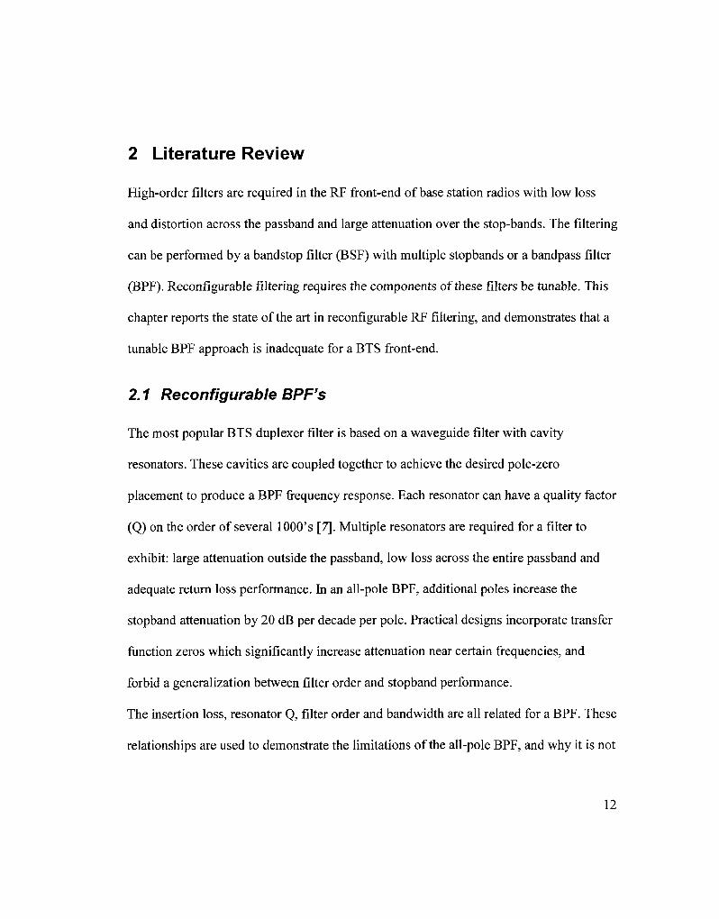
13
a suitable configuration for tunable RF filtering in a BTS RF front-end. A Chebyshev
BPF with 0.1 dB of ripple and N resonators is used as the baseline filter in this section.
The insertion loss of this type of filter is close to optimal and the passband magnitude
response exhibits regular behaviour [8].
The design equations associated with the Chebyshev filter are used to derive the LPF
configuration. The BPF configuration is calculated using a lowpass to bandpass
transformation. The insertion loss of the LPF filter with a maxima at co=0 is related to the
LPF element quality factor (q) by: IL=HL(s)\s=\/q [8]. HL{s) is the transfer function of the
TV111 order 0.1 dB ripple Chebyshev LPF with the cut-off frequency normalized to unity.
The relationship between q and the insertion loss is shown in Fig. 2.1.1 for various LPF
orders (N).
LPF element quality factor (q)
Figure 2.1.1- Insertion loss of 0.1 dB ripple Chebyshev LPF with unity cut-off
frequency
14
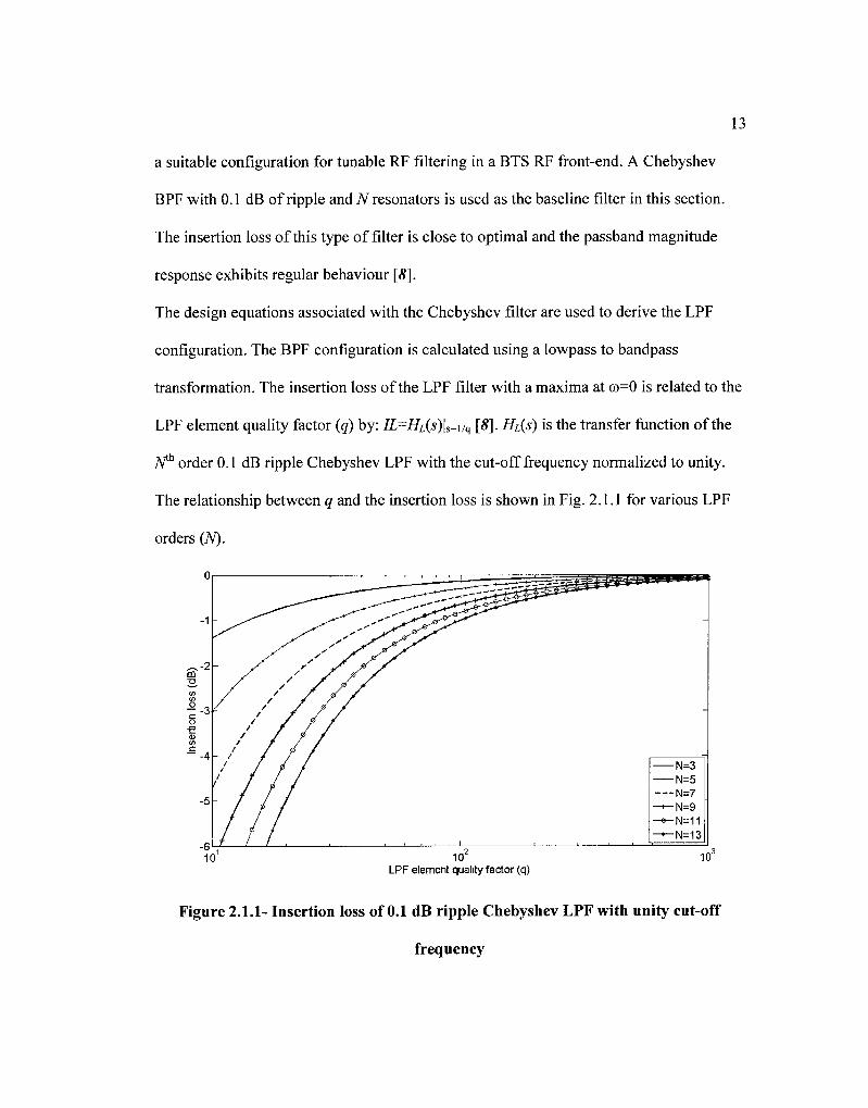
The curves in Fig. 2.1.1 can be used to constrain q based on some insertion loss
threshold. The relationship between the LPF element q, and the BPF resonator Q is:
Q=q/BW [8]. The fractional BWis in terms of a percentage. In Fig. 2.1.2 the insertion loss
is constrained to 1 dB, and the relationship between Q and BWis plotted for various
numbers of resonators (N).
104.
o o .2 >,
O
s V) <u U_ Q. m
'"1 2 3 4 5 6 7 8 9 10 BW (%)
Figure 2.1.2 - Required Q for 1 dB insertion loss of 0.1 dB ripple Chebyshev BPF
The limitations of a BPF approach to RF filtering are illustrated in Fig. 2.1.2. Low
insertion loss, high order and small bandwidth can only be performed by filters that
consist of resonators with quality factors in the order of 1000-10000. These values are
achievable with waveguide based cavity filters, but not with planar or tunable resonators,
with YIG technology as the exception. The procedure that was used to generate Fig. 2.1.2
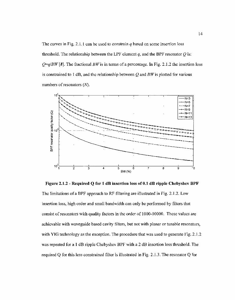
was repeated for a 1 dB ripple Chebyshev BPF with a 2 dB insertion loss threshold. The
required Q for this less constrained filter is illustrated in Fig. 2.1.3. The resonator Q for
15
this less constrained filter is still too high for planar or tunable resonators when the
fractional bandwidth is less than 5% and the number of resonators is greater than 5.
BW (%)
Figure 2.1.3 - Required Q for 2 dB insertion loss with 1 dB ripple Chebyshev BPF
To further demonstrate that tunable BPF's are unsuitable in a BTS RF front-end, the
current state of the art in tunable BPF's is reported. Tunable BPF's are categorized as
either tuning based or switch based. Tuning based resonators employ technologies such
as MEMS capacitors, ferroelectric materials, semiconductor varactors, ferroelectric or
ferrite materials. Switch based tunable resonators use on/off switches to dynamically
change the interconnections between fixed components, such as the capacitors in a
capacitor network. The switches are implemented using technologies such as MEMS
switches or PIN diodes.
2.1.1 MEMS
A resonator can be tuned by mechanically changing some parameter - such as the
separation between the plates of a capacitor. Also, fixed components can be dynamically

16
added or removed from a resonator by using metal contact switches. Both of these
approaches to tuning involve mechanical tuning. MEMS is a popular technology that is
used for mechanically tuning RF components by adjusting an applied DC voltage. Three
types of MEMS components are reviewed: metal-contact switches, capacitive switches
and varactors.
MEMS metal-contact switches and capacitive switches are useful for dynamically
connecting fixed components, like capacitors, to a filter. The quality factor of MEMS
metal-contact switches can be negligible compared to the adjacent fixed components [9].
Capacitive switches are capacitors whose on/off states give a large capacitance ratio such
that when in the off state the component is effectively an open circuit. A large bias
voltage is required to switch to the on state, and fortunately this large voltage prevents the
components from self-switching when the RF input is large. MEMS capacitive switches
can be designed with Q above 100 in the cellular bands [9]. Unlike MEMS capacitive
switches, MEMS varactors can take on a discrete set or continuous range of capacitance
values [9].
A tunable two-pole filter with capacitive switches was reported in [10]. The tuning range
of the centre frequency spanned a discrete set of frequencies between 850 and 1750 MHz.
The passband fractional bandwidth was also tuned from 7 to 42%. Both resonators had an
off-chip inductor with Q greater than 100. Measurements demonstrated a 1 dB insertion
loss across the centre frequency tuning range with the fractional bandwidth fixed at 15%.
The estimated filter Q was 60-90 [9].

17
The Q factor of resonators employing tunable MEMS components is fundamentally
limited by the Q of the surrounding fixed components, like the filter above. This
limitation is most prevalent for planar and discrete components. To realize the potential
of high-Q MEMS, they must be incorporated into resonators with fixed components that
have high Q. Several papers have reported tunable resonator Q factors greater than 200
using MEMS with non-planar resonators. In these papers the resonator consists of a
waveguide cavity with a capacitive post. The resonators are made tunable by using
MEMS components to vary the capacitance of the post. The term 'evanescent mode
waveguide filter' is used in the literature to imply the cross-section dimensions of the
waveguide cavity are significantly smaller than half a wavelength.
A tunable dual cavity evanescent mode waveguide filter was reported in [11] with a
center frequency range that spanned 2.7 to 4.03 GHz. A flexible metalized substrate was
used in place of rigid metal as the top waveguide wall. A piezoelectric actuator deflected
the flexible substrate to vary the spacing between the top waveguide wall and the top of
the fixed capacitive posts inside the cavity. Varying this spacing varies the capacitance of
the post, thereby varying the resonant frequency of the resonator. Measured results of this
2 pole filter showed a fairly consistent 1.3 dB insertion loss with a 2% fractional
bandwidth across the tuning range. A second filter was fabricated that measured a 4.46
dB insertion loss for a fractional bandwidth of 0.5%. Only one tuning point was reported
for the latter filter in [11]. The quality factor of a single resonator was measured, and
varied from 360 at 2.3 GHz to 702 at 4.6 GHz.

18
A different flexible diaphragm evanescent mode waveguide filter with a capacitive post
was reported in [12]. The diaphragm was deflected using electrostatic actuation. The
diaphragm and a second fixed parallel plate had a potential difference applied which
caused the diaphragm to move relative to the fixed plate. A single resonator was
fabricated. The resonator was tuned from 3.42 to 6.16 GHz, and the corresponding
measured quality factor varied between 460 and 530.
A more recent high-Q non-planar tunable filter based on evanescent waveguide
resonators was reported in [13]. The capacitance of the post was varied in this filter by
incorporating RF MEMS switch capacitors between the top of the posts and the top
waveguide wall. A 2 pole filter was fabricated with a nominal fractional bandwidth of
0.5%. The center frequency range of the filter was tuned from 4.07 to 5.58 GHz. Over
this range the fractional bandwidth increased from 0.44 to 0.74%, and the insertion loss
increased from 3.18 to 4.91 dB. The quality factor of the filter was reported to vary from
300 to 500 over the tuning range. The primary limiting factor on Q was the effect of the
bias lines running through the resonator that are required to control the MEMS
components.
The state of the art in high Q MEMS tunable filters has been reported. The Q of planar
filters incorporating MEMS metal contact switches and capacitive switches is limited by
the fixed components. Fixed planar or discrete components do not have sufficient Q for a
BTS RF front-end. The cavity resonators incorporating MEMS have Q up to 700 at
frequencies well above the cellular bands. This optimum Q factor degrades as the
frequency tunes away from the optimum. It is expected that the Q factor of cavity
19
resonators with MEMS will continue to increase in the cellular bands through research
efforts. But like fixed cavity resonators, great efforts are required for relatively small
improvements.
2.1.2 Varactor Diodes
PN junction diodes exhibit a voltage variable capacitance and resistance when reverse
biased. A single varactor has a non-linear C-V curve which limits a varactor's linearity.
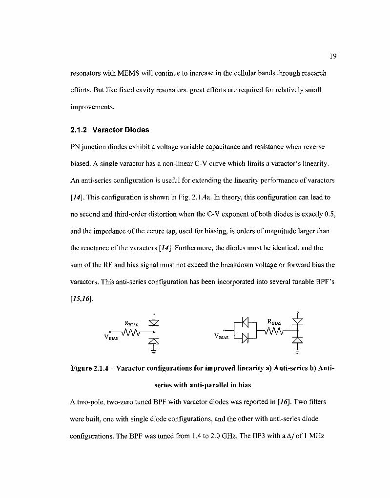
An anti-series configuration is useful for extending the linearity performance of varactors
[14]. This configuration is shown in Fig. 2.1.4a. In theory, this configuration can lead to
no second and third-order distortion when the C-V exponent of both diodes is exactly 0.5,
and the impedance of the centre tap, used for biasing, is orders of magnitude larger than
the reactance of the varactors [14]. Furthermore, the diodes must be identical, and the
sum of the RF and bias signal must not exceed the breakdown voltage or forward bias the
varactors. This anti-series configuration has been incorporated into several tunable BPF's
[15,16].
i H<h RBIAS ^f RBIAS - ¥—
/—MAr VBIAS H^ -VW\r _ ^ _ ^ ^ _
Figure 2.1.4 - Varactor configurations for improved linearity a) Anti-series b) Anti-
series with anti-parallel in bias
A two-pole, two-zero tuned BPF with varactor diodes was reported in [16]. Two filters
were built, one with single diode configurations, and the other with anti-series diode
configurations. The BPF was tuned from 1.4 to 2.0 GHz. The IIP3 with a A/of 1 MHz

20
ranged from 22 to 41 dBm across the range of bias voltage for the anti-series
configuration filter. These IIP3 values were 13-15 dB higher than the single diode
configuration filter. The IIP3 improvement reduced to 6 and 7 dB when Af was less than
the filter's 3-dB bandwidth. The diodes used for the two filters were not identical. The
resonator Q for the single diode configuration filter varied from 72 to 95 over the tuning
range. That for the anti-series diode configuration filter varied from 56 to 125. These
resonator Q factors are close enough to expect the IIP3 improvement to be almost
completely due to the difference in diode configurations. The finite third order distortion
was attributed to the finite impedance of the bias resistor (lOkQ) and the C-V exponent of
the diodes being 0.47 and not the ideal 0.5.
A monolithic silicon-on-glass varactor-based BPF was reported in [15] that was tuned
from 2.5 to 3.5 GHz with a bias from 1 to 13.5 V. One of the constraints for linearity is
the bias network impedance must be significantly larger than the varactor reactance. This
condition must hold over frequencies containing linear and non-linear components. The
reactance of the varactor is (2nCJ)"\ where C is the varactor capacitance. In a two tone
test there is a 2nd order frequency component atj=f\-fi, which can encounter a very large
varactor reactance when the difference between f\ and/ is small. In this scenario the
distortion would not cancel between the two varactors, and was the reason the IIP3
dropped in [16] when A/of the 2 tone test was reduced. This limitation was overcome in
[15] by cascading the bias resistor (RBi) in Fig. 2.1.4a with an anti-parallel varactor
configuration, as shown in Fig. 2.1.4b. The filter had one pole and one zero with a pole-
zero spacing of 400 MHz. The varactor Q varied from 100 to 600 for 5 to 20 pF at 2
21
GHz. An IIP3 of 46 dBm was measured for two signals in the stopband with a A/of 2
MHz. The same IIP3 was also measured for a two-tone input in the passband. This IIP3
was for the lowest DC bias voltage of 1 V. The Q of the resonators was not reported.
The maximum variation in capacitance for a diode varactor occurs for low bias voltages,
but it cannot support a large AC voltage swing at low bias voltages. If the voltage swing
is larger than the bias voltage, then the diode can transition into the forward bias region.
In the front-end of a BTS the potential for this undesirable large signal behaviour is
problematic. Furthermore, the Q factors from the papers reviewed did not meet the
criteria for a BTS front-end.
2.1.3 PIN Diodes
Like MEMS, semiconductor components can be used in tunable filters for variable
capacitance, like varactor diodes, or for switching, like PIN diodes. PIN diodes are used
for dynamically changing connectivity between fixed components. Unlike MEMS
switches, PIN diodes need to be biased with a DC current to provide a short circuit
through the diode [17]. The DC current increases with linearity demands. The advantage
of PIN diodes over MEMS is their compatibility with standard fabrication techniques.
Switches limit the number of configurations that a tunable filter can realize. A large
number of switches can be used to effectively realize any practical configuration. But
PIN diodes are not the optimal technology for a large switching matrix due to their power
demands.
22
2.1.4 Ferroelectric
Ferroelectric varactors are fabricated with ferroelectric materials using thin-film or thick-
film processes. The permittivity of ferroelectric materials is dependent upon an applied
external electric field. The most popular material for ferroelectric varactors in the
literature is barium strontium titanate (BST). Thick-film processes have higher linearity
than thin-film, but require a higher tuning voltage - up to several hundred volts [18].
Thick-film processes are limited to planar structures such as coplanar waveguide or
interdigital capacitor, and the material Q is generally lower than thin-film.
Ferroelectric varactors are commercially available from Paratek and Agile RF. Two
tunable BPF's were reported in [19], which used tunable thin-film capacitors from
Paratek. These varactors had a tuning range of 4.15:1 with a control voltage of 0 to 27 V,
and a Q factor over 100 from 100 to 1000 MHz [19]. A two-pole BPF was tuned from
300 to 450 MHz with a control voltage of 0 to 22 V. The worst case insertion loss was
1.63 dB. An IIP3 of 40 dBm was measured with two input signals in the passband
separated by 2 MHz. A three-pole BPF was also fabricated and measured with the same
voltage control range. The three-pole BPF was tuned from 230 to 400 MHz and had a
worst case insertion loss of 2.5 dB.
More recently a thin-film BST varactor demonstrated a Q factor from 100 to 350 over the
tuning range of 0 to 8 V at 1 GHz [20]. This high Q was obtained by using a nano-
structured thin film BST. Large area pulsed laser deposition was used for depositing the
thin-film. The largest Q factor for BST varactors near 1 GHz is the 100-350 range

23
reported in [20]. This state of the art performance for BST is still too low for a BTS front-
end.
2.1.5 Ferrite
Ferrite materials have some properties at microwave frequencies that have put them into
the front-end of radios as circulators, isolators, absorption type tunable BPF's and BSF's,
and frequency selective power limiters [21]. Ferrites exhibit ferrimagnetic resonance in
the presence of a saturating DC magnetic field. Essentially, a majority of electrons in a
ferrite material tend to align their spin axes when biased by a DC magnetic field of
sufficient magnitude. Ferrites have very low conductivity at microwave frequencies;
therefore they exhibit low conductor loss.
Ferrite BPF's take advantage of the highly selective nature of a ferrite at the material's
resonant frequency. The linewidth of a ferrite can be very narrow such that the unloaded
Q factor can be in the range of 2000 to 10 000 [21]. YIG is the ferrite with the narrowest
linewidth, which is the reason it is popular in ferrite filters requiring high Q.
In ferrite resonators signals are coupled into the fundamental mode, which is called the
uniform precession mode. The resonant frequency of this mode depends primarily on the
external DC magnetic bias and the geometry. A sphere shape resonator with a high
surface polish is required to limit the number of natural resonant modes over the
operating frequency range. The sphere must be small to ensure the magnitude of the input
RF signal is constant across the YIG, otherwise undesired resonator modes are excited
[22]. A ferrite sphere resonator with wire loops used as the coupling mechanisms is
shown in Fig. 2.1.5. The input and output coupling networks are placed perpendicular to
24
one another to use the resonator as a bandpass filter. The input signal coupled into the
uniform precession mode is subsequently coupled to an output coupling network.
Figure 2.1.5 - Ferrite sphere BPF
The high Q property of ferrites breaks down when used at low frequencies. Small DC
bias fields are required for resonance at a low frequency, but if the DC bias field is too
small then the ferrite will not be completely magnetized. If not completely magnetized
then domain-wall motion causes magnetic losses. The Q factor of a YIG sphere reduces
to 0 as the frequency reduces to 1670 MHz [21]. The low-frequency limit can be reduced
by doping the YIG or using a different shape like a disc. The low-frequency limit for Ga-
doped YIG is 1000 MHz [21]. Using a disc can reduce this cutoff frequency to alrrfost 0
[21]. Doping YIG and using non-spherical geometries can degrade the Q factor due to
excitation of higher order modes. Essentially for operation over the 1-2 GHz range the Q
factor of the resonator will not be multiple 1000's, so it will not meet the minimum Q
required in a BTS front-end. Other drawbacks of ferrites are temperature dependency,
IMD, fabrication complexity, and the power required to bias the material with an
electromagnet.
The preceding review represents the state of the art in tunable RF filtering with a BPF
approach. These approaches have demonstrated large tuning ranges, but are limited to

25
low order filters due to the relatively low Q-factors of the tunable resonators. These
characteristics do not meet the filtering requirements of a BTS RF front-end.
2.2 Reconfigurable Multiple Stopband Filters
BPF's have become the filter configuration of choice for fixed-frequency filtering in the
RF front-end of a BTS. But the lack of a suitable high Q and highly linear tunable
resonator thwart the possibility of a frequency agile BPF with acceptable performance.
A different approach for tunable RF filtering is based on creating multiple stopbands or
notches. Multiple stopband or notch filters must adapt to the input RF environment to
keep the notches collocated with undesired signals outside the passband. Multiple notch
filters are implemented as all-zero filters. The locations of the zeros correspond to the
notches in the frequency response. If tunable RF resonators are used to implement the
zeros, then resonator Q will limit the maximum filter order as with the BPF
configuration. A different all-zero technique is based on feed-forward (FF). FF systems
attempt to perfectly cancel part of an RF signal using one or more copies of that signal. In
this section the state of the art in RF FF attenuation is presented. RF FF has more heritage
in the field of power amplifier (PA) linearization than in RF filtering. FF amplifier
linearization is reviewed prior to the state of the art of FF RF filtering.
2.2.1 FF Amplifier Linearization
FF amplifier linearization is a technique that reduces the output distortion of a non-linear
PA. A typical FF amplifier linearization system is shown in Fig. 2.2.1a. This system
consists of two FF cancellation loops: the signal cancellation loop and the error
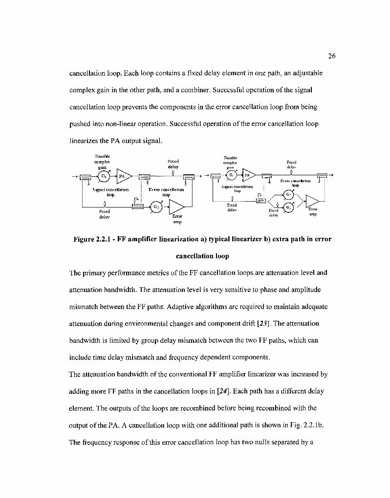
26
cancellation loop. Each loop contains a fixed delay element in one path, an adjustable
complex gain in the other path, and a combiner. Successful operation of the signal
cancellation loop prevents the components in the error cancellation loop from being
pushed into non-linear operation. Successful operation of the error cancellation loop
linearizes the PA output signal.
TunaHe complex
gain
w^sH^^ Fixed delay
Signal cancellation loop
Fixed delay
Figure 2.2.1 - FF amplifier linearization a) typical linearizer b) extra path in error
cancellation loop
The primary performance metrics of the FF cancellation loops are attenuation level and
attenuation bandwidth. The attenuation level is very sensitive to phase and amplitude
mismatch between the FF paths". Adaptive algorithms are required to maintain adequate
attenuation during environmental changes and component drift [23]. The attenuation
bandwidth is limited by group delay mismatch between the two FF paths, which can
include time delay mismatch and frequency dependent components.
The attenuation bandwidth of the conventional FF amplifier linearizer was increased by
adding more FF paths in the cancellation loops in [24]. Each path has a different delay
element. The outputs of the loops are recombined before being recombined with the
output of the PA. A cancellation loop with one additional path is shown in Fig. 2.2.1b.
The frequency response of this error cancellation loop has two nulls separated by a
27
frequency offset. Both of the complex gain elements drift; therefore they need to be
tracked by an adaptive algorithm. The adaptive algorithms used in [24] decorrelate the
signals within each branch before independently correlating the results with the FF output
signal.
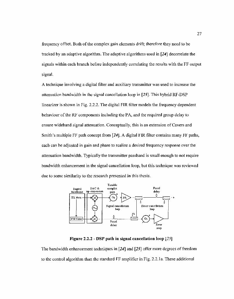
A technique involving a digital filter and auxiliary transmitter was used to increase the
attenuation bandwidth in the signal cancellation loop in [25]. This hybrid RF-DSP
linearizer is shown in Fig. 2.2.2. The digital FIR filter models the frequency dependent
behaviour of the RF components including the PA, and the required group delay to
ensure wideband signal attenuation. Conceptually, this is an extension of Cavers and
Smith's multiple FF path concept from [24]. A digital FIR filter contains many FF paths,
each can be adjusted in gain and phase to realize a desired frequency response over the
attenuation bandwidth. Typically the transmitter passband is small enough to not require
bandwidth enhancement in the signal cancellation loop, but this technique was reviewed
due to some similarity to the research presented in this thesis.
Tunable Digital DAC & complex
baseband up-conveision g a m
TX data —H—•fX') 1 K Gl
FLRfuteil
Fixed delay
PA
Signal cancellation loop
m Fixed delay
Erior cancellation loop
- (<* Eiror amp
Figure 2.2.2 - DSP path in signal cancellation loop [25]
The bandwidth enhancement techniques in [24] and [25] offer more degrees of freedom
to the control algorithm than the standard FF amplifier in Fig. 2.2.1a. These additional
28
degrees of freedom require more complex adaptive algorithms to maintain adequate
attenuation performance. The remainder of this section is a survey of RF FF attenuation
used in filtering applications.
2.2.2 Interferer Attenuation in Receiver
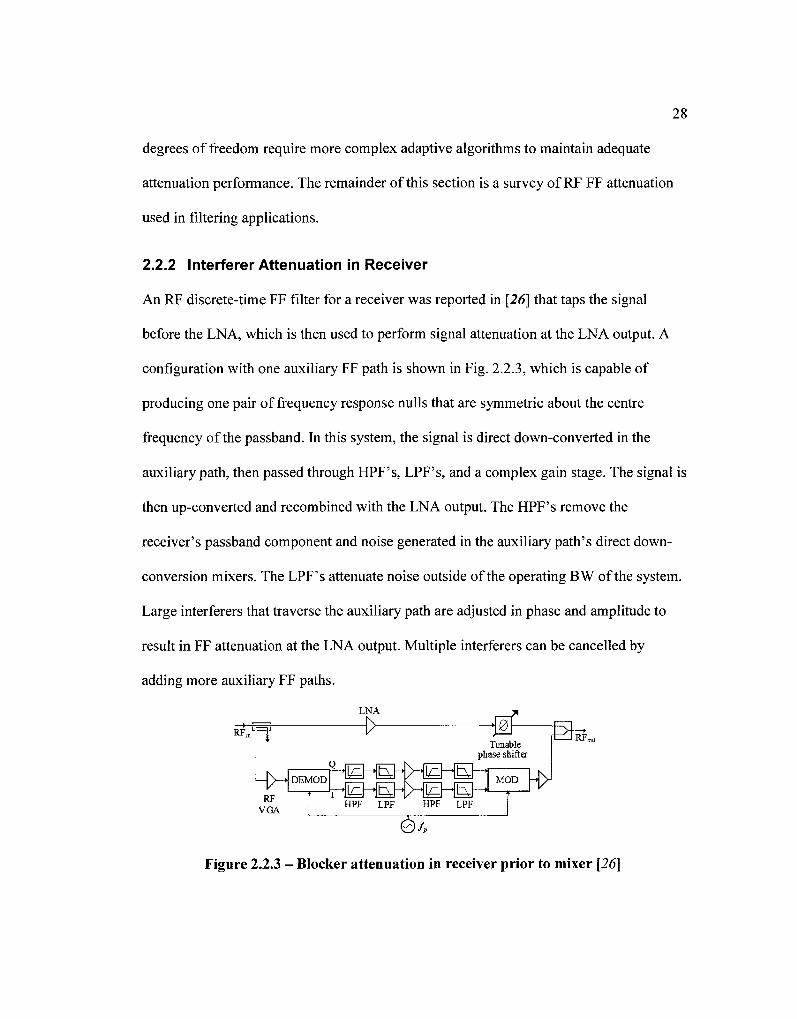
An RF discrete-time FF filter for a receiver was reported in [26] that taps the signal
before the LNA, which is then used to perform signal attenuation at the LNA output. A
configuration with one auxiliary FF path is shown in Fig. 2.2.3, which is capable of
producing one pair of frequency response nulls that are symmetric about the centre
frequency of the passband. In this system, the signal is direct down-converted in the
auxiliary path, then passed through HPF's, LPF's, and a complex gain stage. The signal is
then up-converted and recombined with the LNA output. The HPF's remove the
receiver's passband component and noise generated in the auxiliary path's direct down-
conversion mixers. The LPF's attenuate noise outside of the operating BW of the system.
Large interferers that traverse the auxiliary path are adjusted in phase and amplitude to
result in FF attenuation at the LNA output. Multiple interferers can be cancelled by
adding more auxiliary FF paths.
LNA *
RF,„ rt i>-
^ DEMOD
RF VGA
Tunable phase shifter
MOD
HPF LPF HPF LPF
V
RFm
Figure 2.2.3 - Blocker attenuation in receiver prior to mixer [26]
29
A hardware prototype was reported in [26] with discrete components and one auxiliary
path, like Fig. 2.2.3. A 20 dB coupler was used to extract the input signal for the auxiliary
path. A phase shifter was placed in the main path and an RF VGA in the auxiliary path.
The HPF's had a comer frequency of 2 MHz, and the LPF's had a comer frequency of 16
MHz. The LPF's were found to improve the output noise floor by 2 dB. One realization
of the VGA and phase shifter settings resulted in a 26.2 dB null at 5.9 MHz below the
passband centre frequency (880 MHz), and a 23.5 dB null at 4.4 MHz above. The 20 dB
attenuation BW was approximately 0.27 and 0.17 MHz for the upper and lower sideband
notches, respectively.
A second hardware prototype was built from discrete components that had two auxiliary
paths to permit attenuation of two interferers. A phase shifter was placed into each of the
auxiliary paths, instead of the main path. One realization of the VGA and phase shifter
settings resulted in a 25 dB null at 10.35 MHz above the passband centre frequency (870
MHz), and a 15 dB null at 20 MHz above. Results in the lower sideband were not
reported. The 20 dB attenuation BW of the deeper notch was approximately 1 MHz.
Simulations were used to demonstrate proper operation of a system with multiple
auxiliary paths, but only required one demodulator and modulator. Several copies of the
IQ outputs of the demodulator are sent to different baseband paths. These paths are
uncorrelated by putting a different non-overlapping BPF in each path. The amplitude and
phase adjustment in one frequency sub-band does not impact the frequency response
outside this sub-band.
30
A BTS requires a high order filter; therefore would require multiple auxiliary paths. As
the number of auxiliary paths increase, so does the number of analog components which
drift with age and environmental changes. A control algorithm was not reported in [26],
but would need to track this drift. The frequency spacing between sub-band filters should
be no more than the expected frequency separation between interferers. This constraint
could result in an unmanageable number of sub-band filters. Furthermore, these sub-band
filters would need to partially overlap to avoid dead spot frequencies that the FF system
cannot attenuate. The FF system in [26] is limited to relatively low order, which is useful
for attenuation of a few interferers that are adequately separated in frequency.
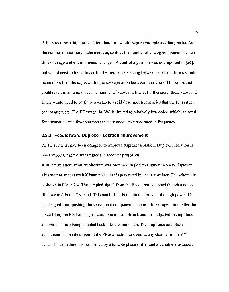
2.2.3 Feedforward Duplexer Isolation Improvement
RF FF systems have been designed to improve duplexer isolation. Duplexer isolation is
most important in the transmitter and receiver passbands.
A FF active attenuation architecture was proposed in [27] to augment a SAW duplexer.
This system attenuates RX band noise that is generated by the transmitter. The schematic
is shown in Fig. 2.2.4. The sampled signal from the PA output is passed though a notch
filter centred in the TX band. This notch filter is required to prevent the high power TX
band signal from pushing the subsequent components into non-linear operation. After the
notch filter, the RX band signal component is amplified, and then adjusted in amplitude
and phase before being coupled back into the main path. The amplitude and phase
adjustment is tunable to permit the FF attenuation to occur at any channel in the RX
band. This adjustment is performed by a tunable phase shifter and a variable attenuator.
31
Transmitter M >
TT
y Duplexer ln
ErhMS> LN/> Receiver
notch complex filter gain
Figure 2.2.4 - FF attenuation to receiver [27]
The SAW duplexer contributed to a relatively large group delay mismatch between the
two FF paths. In FF systems, the attenuation bandwidth narrows as the group delay
mismatch increases [23]. Multiple FF paths were proposed in a parallel configuration for
attenuation at multiple frequencies, or for a wider attenuation bandwidth.
The system was fabricated with a single FF path in [27]. The TX band was 824-849 MHz
and the RX band was 869-894 MHz. The SAW duplexer had 40 dB of TX-RX isolation
in the RX band. The active cancellation system increased the isolation by more than 20
dB over a 2 MHz channel bandwidth. This performance was reported for each channel in
the RX band. A system with dual error paths was also built and tested. The results for two
different cases were reported. The first case placed the two frequency response nulls 9
MHz apart, and the resulting improved isolation was 9 dB over 16 MHz. The second case
had a null spacing of 4 MHz, whereby the isolation increased by 20 dB over 4.5 MHz.
The insertion loss for both the transmit and receive chain was 0.27 dB. The control
signals in the gain and phase adjuster were manually tuned.
Tunability of the RX channel within the RX band was demonstrated. The TX band was
not tunable, due to the fixed notch filter. The proposed system did not isolate the receiver
from the portion of the transmit signal that is reflected back from the antenna. A second
32
system was proposed that is identical to that in Fig. 2.2.4, except the signal is re-injected
into the antenna port of the duplexer to cancel antenna reflections. This system would
need the same components as that in Fig. 2.2.4, thereby doubling the total number of
components.
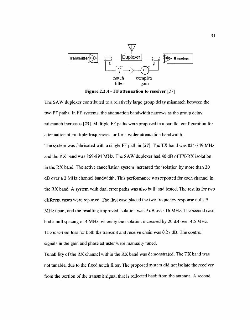
A system with two FF cancellation loops was reported in [28] to improve duplexer
isolation in a BTS. This system is located at the output of the TX chain, and is designed
to cancel noise generated by the transmitter in the RX band. A block diagram is shown in
Fig. 2.2.5. At the output of the transmitter, the TX band signal is much larger than the RX
band noise. The TX band signal must be attenuated prior to passing it through
components that operate on the RX band signal; otherwise the components would be
pushed into non-linear operation. An additional FF cancellation loop is used to perform
this TX band attenuation. The first loop in Fig. 2.2.5 is the signal cancellation loop. Since
the loop uses FF attenuation, it can be tuned to permit a frequency agile TX band. The
error cancellation loop in Fig. 2.2.5 performs the RX band attenuation. Both cancellation
loops have a complex multiplier, which is implemented with a vector modulator cascaded
with an amplifier. Since both loops are independently tuned, the FDD separation can
vary. A reference signal is injected near the RX channel, which is measured after the
single path cancellation. This measurement is used to manually tune the control signals.
The band used in this work was at 1900 MHz. Simulation results showed 32 dB of
attenuation in the error cancellation loop over a 5 MHz RX channel with an FDD
separation of 5 MHz [28]. The signal cancellation loop attenuation was greater than 20
33
dB over the TX channel. The error cancellation loop attenuation corresponds to the
improvement in duplexer isolation over the RX channel.
HJ
Fixed delay V
PA
Signal cancellation loop
H& a, Fixed
Tunable delay complex
gain
rt n i i ror cana
loop Ei ror cancellation
loop
Dup exer £> Receiver
Error amp
Figure 2.2.5 - Frequency agile BSF schematic [28]
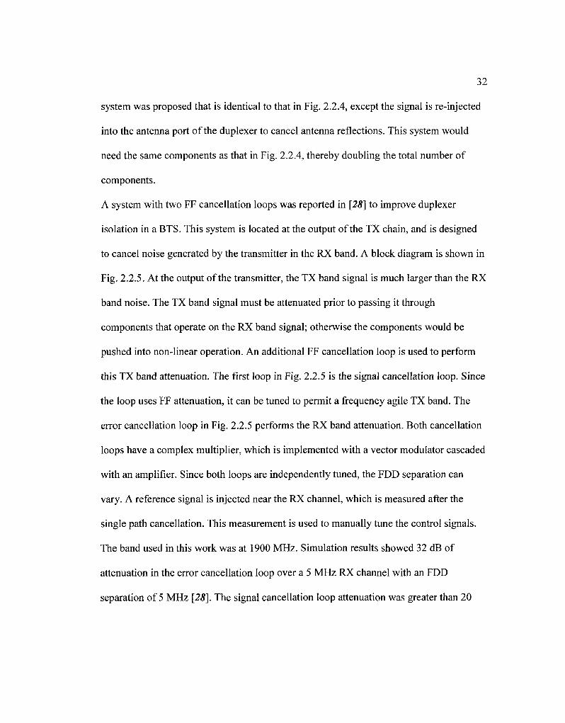
The two preceding systems reviewed improve duplexer isolation in the RX band.
Inadequate isolation over the TX band will result in the high power signal leaking into
the receiver and potentially desensitizing the receiver. In [29] an auxiliary transmit chain
is used to generate an RF signal that cancels the transmitter leakage in the receiver. This
system improves isolation only in the TX band. The attenuation occurs between the
duplexer and the LNA, as shown in Fig. 2.2.6. The input to the auxiliary transmitter is the
same digital signal that is sent to the main transmitter, except it goes through an
additional digital FIR filter. This filter is designed to have a transfer function that models
the transmitter chain components including antenna reflections. A wideband training
sequence is sent through the transmitter, which is used to calculate the filter coefficients.
34
Digital in
Transmitter P,
y Duplexer
FIR Filter
Auxiliary transmitter
Llfe> Receiver
Figure 2.2.6 - Auxiliary transmitter attenuation [29]
The test setup included a fixed wideband duplexer that provided 25 dB of isolation
between the main transmitter and the receiver. For a TX signal with a 5 MHz bandwidth
centered at 1.96 GHz, the additional isolation provided by the auxiliary transmit chain
was 35 dB. This result was similar for a narrow band signal centered at 2.02 GHz. This
paper demonstrated wideband attenuation without the use of multiple RF cancellation
paths. Adaptive control of the FIR was recommended for optimal performance, but was
not implemented in the demonstrator.
The cancellation signal is a linear function of the baseband signal. The cancellation signal
cannot cancel the IMD or noise generated by any of the transmitter components.
Furthermore, any noise or IMD generated by the auxiliary transmitter in the RX band
decreases the sensitivity of the receiver. Large attenuation performance is limited to
transmitters with low noise and highly linear components.
In [30] a FF attenuation system was developed to enhance a fixed duplexer by improving
duplexer isolation in both the TX and RX bands. The fixed duplexer used for the
measurements provided at least 20 dB of isolation in both bands. The dual feed-forward
path topology is shown in Fig. 2.2.7. Vector attenuators were used in the FF paths to
adjust the phase and amplitude.
35
Transmitter F>5f> L T V
Duplexer
-, 0 /T<,
T J L^> Receiver
Fixed delay
Figure 2.2.7 - Double loop attenuation [30]
In [57], measured results were published with a TX band centered at 1955 MHz, and a
RX band at 2145 MHz for the system in Fig. 2.2.7. The attenuation circuit increased the
TX band isolation by 47 dB and the RX band by 38 dB. The attenuation was measured
over 5 MHz channel bandwidths.
A pilot tone near the centre of the RX band was coupled into the main path in the
transmitter, then down converted and sampled in the receiver and used as an error signal.
A control algorithm automatically tuned the signal adjusters in the FF paths.
This system was designed for a mobile terminal, not a BTS. The dynamic range of the
BTS transmit signal between the TX band and RX band is much larger than mobile
equipment. This would require vector modulators with the same dynamic range in the FF
paths, which is infeasible for typical BTS requirements.
The state of the art in RF FF attenuation systems has been reviewed. A large attenuation
bandwidth is achievable by minimizing the delay mismatch between the FF paths, or by
increasing the number of FF paths. A large number of FF paths is undesirable at RF due
to the complexity involved with splitting and combining RF signals, and compensating
for all of the frequency dependent components and drift. These limitations have limited
the FF systems reviewed to two paths.

36
2.3 Summary of Literature Review
The Q-factor of tunable resonator based filters results in unacceptable insertion loss in
high-order configurations. RF FF filters provide low insertion loss, and high order
filtering is possible by increasing the number of FF paths. But, each additional FF path
requires an additional signal splitter, tunable complex gain components, and signal
combiner. The increase in components, power, space, and control circuitry may not be
justifiable for each increase in the filter order for a high-order filter.

3 System Description
In this research a hybrid RF-DSP FF filter has been developed that exhibits low loss in
high-order configurations. Increasing the order of this filter only requires an additional
tap in a digital FIR filter. The purpose of this chapter is to substantiate the configuration
and each module down to the component level. The latter part of this chapter specifies
how this filter integrates into an RF front-end.
3.1 System Architecture
The hybrid RF-DSP FF filter consists of two paths in a FF configuration, and a feedback
path for filter adaptation. One of the FF paths contains only RF components, and the
other has a digital filter along with frequency up and down conversion circuits. The path
with the digital filter also contains a tunable BSF. One configuration of the hybrid RF-
DSP FF filter is shown in Fig. 3.1.1. Both FF paths start at the coupler denoted C\, and
end at C2. The feedback path starts at the coupler denoted C3, and ends at the algorithm
processor.
37
38
c^ jj c2 c3
1 J Fixed delay r \yyjm
RF/ Analog 1
p Digital Filter
t
Algorithm processor
RF/ Analog 2
Tunable RSF
T
j L
H RF/
Analog 3
Figure 3.1.1 - System-level schematic of hybrid RF-DSP FF filter
FF configurations provide transfer function zeros. A transfer function zero can be
constrained to provide a deep notch in the frequency response. A deep notch is realized
when the signals in the two paths have equal magnitudes and a 180° phase difference at
C2. Each additional path in a FF configuration provides an additional transfer function
zero. The digital filter in Fig. 3.1.1 is of the FIR type, and each filter tap provides a
transfer function zero to the overall hybrid RF-DSP FF filter. The FIR filter can have a
large number of taps, which means the entire FF filter can have a high-order all-zero
frequency response. Essentially, the digital filter adjusts the magnitude and phase of
signals in different bands to ensure adequate attenuation at the RF output of the hybrid
RF-DSP FF filter.
The remaining components in the FF path containing the digital filter permit the digital
filter to be used in an RF system. The RF/Analog modules in Fig. 3.1.1 that bookend the
digital filter provide frequency conversion between RF and baseband. Varying the LO
frequency to these modules varies the RF centre frequency of the system. The BSF
increases the lower FF path's dynamic range, which is necessary due to the quantization
noise inherent to the digital components.
39
The upper FF path provides the means for the desired passband signal to pass through the
filter with minimal loss and distortion. In the simplest configuration the RF path is a
transmission line. The insertion loss of this path is that of the thru ports of the three
directional couplers and any transmission line loss. The insertion loss of the hybrid RF-
DSP FF filter is independent of filter order and can be less than 1 dB by using 10 or 20
dB directional couplers for C\, Cj and C3. Other RF components can be placed in this
path, and some examples are shown later in this chapter. The dynamic range, power
handling, passband distortion and noise of the hybrid RF-DSP FF filter depend primarily
on the performance of the lower FF path.
The block diagram from Fig. 3.1.1 is shown in more detail in Fig. 3.1.2. The algorithm
processor has been omitted from this figure for clarity. The lower FF path starts at the
coupled port of coupler C\, and ends at the coupled port of coupler C2. The
'RF/Analog 1' block consists of an amplifier, demodulator, LPF's, and two ADC's. The
ADC's feed a digital FIR filter. The digital filter adjusts the phase and magnitude of
signals within the bands where FF attenuation is desired. The output of the digital filter
feeds the DAC's in the 'RF/Analog 2' block. This block also consists of LPF's, a
modulator and an amplification stage. Before being re-injected back into the upper FF
path, the signal is filtered by a tunable BSF. The BSF exhibits a notch over the band
where the noise figure of the hybrid RF-DSP FF filter must be minimal and no
attenuation is required. The coupled port of the third directional coupler sends the hybrid
RF-DSP FF filter's output signal through an amplification and frequency conversion
stage. The signal is then digitized and used by adaptive algorithms in the algorithm
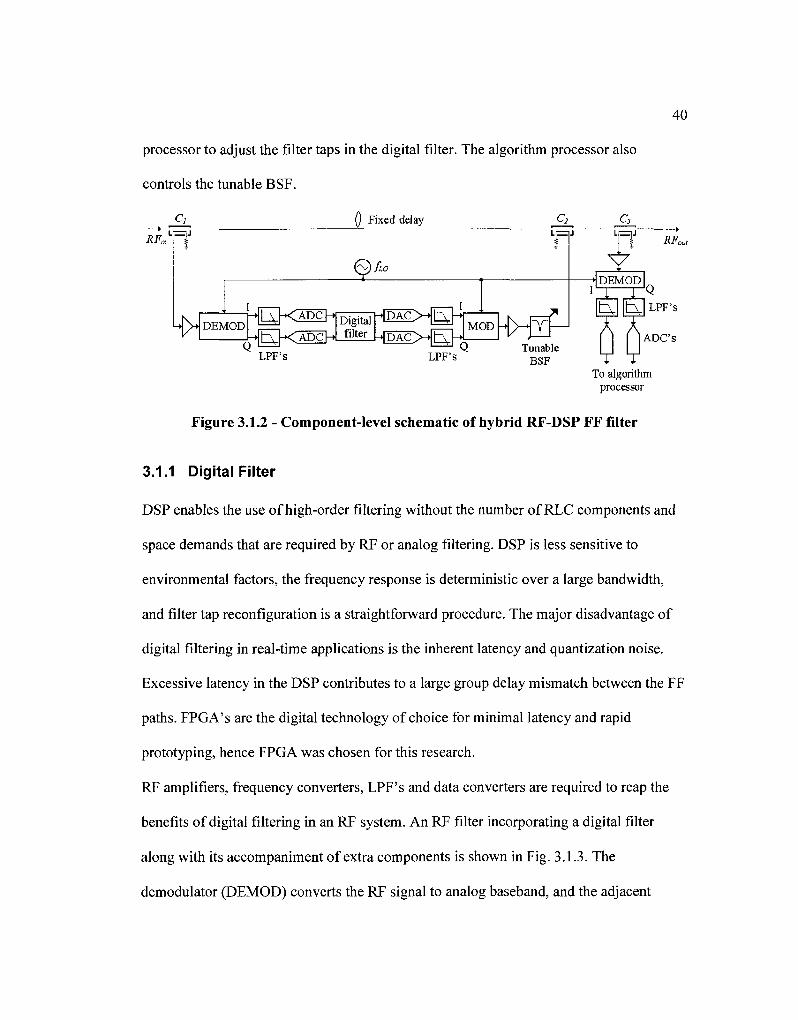
40
processor to adjust the filter taps in the digital filter. The algorithm processor also
controls the tunable BSF.
Fixed delay C,
RF,„LF^
4>
fy&
LnJ p
DEMOD h , -<ADC]
|-A t-<ADC}
5i^alH2A^MU filter
UDAC>>[E^ MOD -i EH
RF*
DEMOD
iS: Q u u
LPF's LPF's Tunable
BSF
LPF's
ADC's
To algorithm processor
Figure 3.1.2 - Component-level schematic of hybrid RF-DSP FF filter
3.1.1 Digital Filter
DSP enables the use of high-order filtering without the number of RLC components and
space demands that are required by RF or analog filtering. DSP is less sensitive to
environmental factors, the frequency response is deterministic over a large bandwidth,
and filter tap reconfiguration is a straightforward procedure. The major disadvantage of
digital filtering in real-time applications is the inherent latency and quantization noise.
Excessive latency in the DSP contributes to a large group delay mismatch between the FF
paths. FPGA's are the digital technology of choice for minimal latency and rapid
prototyping, hence FPGA was chosen for this research.
RF amplifiers, frequency converters, LPF's and data converters are required to reap the
benefits of digital filtering in an RF system. An RF filter incorporating a digital filter
along with its accompaniment of extra components is shown in Fig. 3.1.3. The
demodulator (DEMOD) converts the RF signal to analog baseband, and the adjacent

41
LPF's are used for anti-aliasing. The ADC's and DAC's are used to interface the analog
baseband and digital domains. Two ADC's and two DAC's are required to transfer the
signals I and Q components. The LPF's following the DAC's are reconstruction filters,
and the proceeding modulator (MOD) converts the analog baseband signal back to RF.
A digital clock signal with frequency Fs is distributed to the data converters and FPGA. A
digital clock frequency of Fs permits the overall RF system to operate over an RF
bandwidth equal to Fs.
Q)FS
I I
RFm
DEMOD |^|-<AI5C1
K -<ADCl
LPF's
Digital filter
FPGA
DACV>|-A
J-«TDAC>»rA MOD
LPF's Q ;:
"<§>
RF„
fie
Figure 3.1.3 - DSP filtering configuration
The quantization noise generated by the digital components degrades the output noise
floor. This degraded noise floor results in a significant drop in dynamic range between
RFm and RF0Ut in Fig. 3.1.3. The output noise floor is most problematic over the filter's
passband. In low noise applications a BSF, tuned to the passband, is placed after the
modulator to minimize this degradation to the noise floor. Consequently, the passband
frequency response of the FF path containing the BSF has a notch over the passband.
With this characteristic, ideally none of the signals in the passband at the output of the
hybrid RF-DSP FF filter have come from the lower FF path.

42
The relationships between the design parameters of the digital components and the noise
and attenuation performance of the FF filter are derived in Chapter 4. The adaptive
algorithms that control the filter taps are derived in Chapter 5.
3.1.2 Direct Up and Down Conversion
The frequency up and down converters that bookend the baseband components enable the
hybrid RF-DSP FF filter to be frequency agile. The RF frequency range of these
components limits the RF frequency range of the entire filter. The LO source for these
components is denoted b y ^ o in Fig. 3.1.3. The following discussion justifies direct
frequency conversion, which inherently has adverse effects near DC.
The LO frequency used by the frequency converters is equal to the centre frequency of
the FF filter's passband. This frequency relationship means the centre frequency of the
passband is mixed down to DC, where flicker noise and DC impairments are at their
worst. After traversing the digital filter, the signals near DC are then up-converted to the
centre frequency of the passband again, and then they are significantly attenuated by the
BSF. Ideally, the BSF removes any signals from the lower FF path that were caused by
flicker noise or DC impairments in the frequency converters. The BSF also removes any
passband signal components that appear at its input. The purpose of the lower FF path is
to adjust the phase and magnitude of signals that need to be attenuated at the FF filter's
output, which does not include the passband. The only contribution to the passband at the
hybrid RF-DSP FF filter's output should be from the upper FF path.
43
3.1.3 Tunable BSF
The BSF attenuates signals and noise within the hybrid RF-DSP FF filter's passband at
RF. In doing so, the BSF increases the dynamic range of the lower FF path. In low noise
applications the BSF is placed after the modulator or after the adjacent RF gain stage.
The centre frequency and bandwidth of the BSF must be reconfigurable to permit the
total filter to have a reconfigurable centre frequency and passband bandwidth. The first
criterion is met by using an RF notch filter with a tunable centre frequency. A
conventional RLC resonator or two-path FF configuration is appropriate to realize the
notch. These filters must be tunable; meaning the former must have a varactor, and the
latter an adjustable complex gain component. The second criterion of the BSF requires
the attenuation bandwidth of the notch response to be tunable. Essentially, signals that are
significantly attenuated by the notch, but fall outside the receiver's passband need to be
boosted. Typically a tunable pole at RF would do the trick. But, these extra RF
components can be avoided by performing the gain compensation in the digital domain -
using an IIR filter.
The attenuation bandwidth of the RF notch filter is narrowed by using gain compensation
in the digital domain with a technique similar to de-emphasis. The goal of gain
compensation is to provide the inverse magnitude response of the RF notch, except
within the passband. A digital IIR filter with a pair of complex conjugate poles and a zero
at z=l can be used to create this desired magnitude response.

44
The notch portion of the BSF cannot be moved to the digital domain. The RF-BSF must
notch noise generated by all of the lower FF path components, including the quantization
noise in the digital components and flicker noise from the modulator.
Integration of the digital de-emphasis and RF notch (RF-BSF) within the lower FF path is
shown in Fig. 3.1.4 and Fig 3.1.5. These two figures show two single order
configurations of the RF notch: the RLC resonator, and the two path FF.
I
RFm DEMOD
|-A -<ADCT->->
b . ,ADC[
LPF's
IIR De-
emphasis
->->1DAC>-»I~\
FPGA
FIR adaPtive U U [ D A C > E
filter l = t
MOO fr LPF's
RFo,
RF-BSF
Figure 3.1.4 - RLC BSF combined digital and RF
RF» DEMOD rjl -HFTl
| - \ - < A D C
t \ - < A D C
LPF's
->->fDAC>-*[Ev
->->fDAC>-»r'\
LPF's RF-BSF
Figure 3.1.5 - FF BSF combined digital and RF
The drawback of the IIR de-emphasis is the additional group delay associated with this
filter, due to the additional registers required for implementation. If the de-emphasis filter
is omitted to minimize the group delay, then the adaptive FIR filter will need to perform
the gain compensation. If the adaptive filter is constrained to perform gain compensation
near the passband edges, then it will have fewer degrees of freedom to cause interferer
attenuation away from the passband.
45
3.2 Applications
The hybrid RF-DSP FF filter is fundamentally different than current state of the art
tunable RF filters. This section illustrates how this novel filter is integrated into the RF
front-end. The filter can be used in the receive chain, in the transmit chain, and across the
terminals of a duplexer.
3.2.1 Applications in the Receive Chain
The hybrid RF-DSP FF filter can be used in the receive chain to attenuate large
interferers to prevent receiver components from being pushed into non-linear operation.
The interference includes self-interference due to leakage of the transmit signal into the
receiver as well as external interferers. The digital filter is used to adjust the amplitude
and phase of the interference signals to result in FF attenuation at the output of the hybrid
RF-DSP FF filter. The high-order filtering characteristic of the filter permits interference
to be cancelled relatively close to the passband, which is required for adjacent channel
rejection and near-band blockers. High-order filtering in a discrete-time RF filter also
permits attenuation of multiple interferers.
The BSF is placed after the frequency up-conversion stage for receive chain applications.
The BSF is used to notch any noise generated by the lower FF path in the receiver's
passband. The tunable BSF also prevents any filtered passband signal from being re
injected back into the main path; otherwise it might combine with the desired receive
signal and result in loss or distortion.
In one configuration the hybrid RF-DSP FF filter is placed between the duplexer and
LNA as shown in Fig. 3.2.1. In this embodiment the upper FF path is a delay line. This
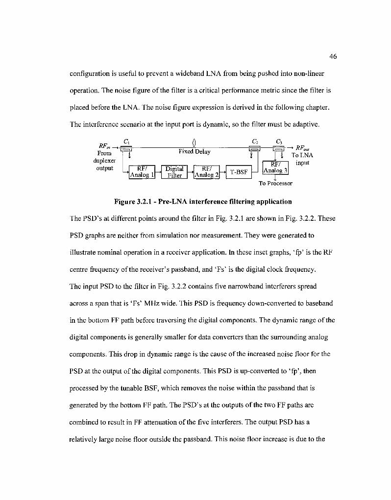
46
configuration is useful to prevent a wideband LNA from being pushed into non-linear
operation. The noise figure of the filter is a critical performance metric since the filter is
placed before the LNA. The noise figure expression is derived in the following chapter.
The interference scenario at the input port is dynamic, so the filter must be adaptive.
RF,„ C,
From | duplexer output
1 Fixed Delay rr nj
RF/ Analog 1
Digital Filter
RF/ Analog 2 T-BSF
RF/ Analog 3
T
To LNA input
To Processor
Figure 3.2.1 - Pre-LNA interference filtering application
The PSD's at different points around the filter in Fig. 3.2.1 are shown in Fig. 3.2.2. These
PSD graphs are neither from simulation nor measurement. They were generated to
illustrate nominal operation in a receiver application. In these inset graphs, 'fp' is the RF
centre frequency of the receiver's passband, and 'Fs' is the digital clock frequency.
The input PSD to the filter in Fig. 3.2.2 contains five narrowband interferers spread
across a span that is 'Fs' MHz wide. This PSD is frequency down-converted to baseband
in the bottom FF path before traversing the digital components. The dynamic range of the
digital components is generally smaller for data converters than the surrounding analog
components. This drop in dynamic range is the cause of the increased noise floor for the
PSD at the output of the digital components. This PSD is up-converted to 'fp', then
processed by the tunable BSF, which removes the noise within the passband that is
generated by the bottom FF path. The PSD's at the outputs of the two FF paths are
combined to result in FF attenuation of the five interferers. The output PSD has a
relatively large noise floor outside the passband. This noise floor increase is due to the
47
noise floor from the bottom FF path. The filter's output signal within the passband at 'fp'
ideally only consists of any signal at 'fp' at the filter's input. This application is useful
when the desired passband signal is low-level.
fp-Fs/2 fp+Fs/2 fp-Fs/2
RFm 1 From
duplexer output
Fixed Delay
RF/ Analog 1
Digital Filter
RF/ Analog 2
-Fs/2
fp
C2 C3
fp+Fs/2
rr n T-BSF - 1
RF/ Analog 3
ToLNA input
T To Processor
Fs/2 fp-Fs/2 fp+Fs/2
I 1 1
-Fs/2 Fs/2
Figure 3.2.2 - PSD at different locations around filter
48
In another configuration the upper FF path could include the LNA, as shown in Fig.
3.2.3. This system provides additional protection to the mixers in the presence of large
interferers, but not the LNA. In this configuration the noise figure of the filter is not as
important as Fig. 3.2.1 since the noise is injected after the LNA. The group delay of the
LNA will reduce the delay mismatch between the upper FF path and lower FF branch,
which improves performance in a FF system.
m* From ^\
duplexer output
D> LNA
RF/ Analog 1
Digital Filter
RF/ Analog 2 T-BSF
-> RF01 Lr=iJ L F=] J out
i i To down-RF/
Analog 3 converter
To Processor
Figure 3.2.3 - System-level schematic of hybrid FF filter
Typically BTS receivers need highly linear down-conversion mixers due to large
interferers. Highly linear mixers are implemented using passive components and are
generally noisier than active mixers due to a large insertion loss. When the configuration
in Fig. 3.2.3 is integrated into a fixed-frequency radio, then the linearity requirements on
the down-conversion mixer can be relaxed, and potentially permit lower noise active
mixers. This configuration would reduce the system noise figure of the receiver.
3.2.2 Application in the Transmit Chain
Typically the signals that need to be attenuated on the receive side of the radio are much
stronger than the signals in the passband. On the transmit side of the radio, typically the
signals to be attenuated are much weaker than the signals in the passband. The weak
signals that are to be attenuated could be IMD, spurious components and noise generated

49
by the preceding transmitter components. The attenuation at the output of the PA can be
performed anywhere outside the transmit passband, including the radio's receive
passband.
The BSF is placed before the down-conversion stage for transmit chain applications and
is tuned to remove the large passband signal. If this signal is not adequately attenuated,
then the down-conversion and digital components will need to adjust the maximum
expected input signal accordingly, which degrades the sensitivity level. Fig. 3.2.4 shows
the configuration for the hybrid RF-DSP FF filter placed between the PA and the
duplexer. A BSF is also placed in the feedback path to prevent the passband signal from
affecting adaptation.
a A c2 c3 RF„
From PA output
—1J Fixed Delay L|=|J
— > T-BSF — • RF/
Analog 1 — • Digital Filter
— • RF/
Analog 2
L 1 J
T-BSF
RF/ Analog 3
To duplexer input
r To Processor
Figure 3.2.4 - Post-PA IMD and spur filtering application
The configuration in Fig. 3.2.4 bears some resemblance to FF amplifier linearization,
where the BSF is implemented using the PA input signal. FF amplifier linearization was
reviewed in Section 2.2.1. There has been no attempt to use a digital filter for the error
cancellation loop in a FF amplifier linearization as shown in Fig. 3.2.4. FF amplifier
linearization performs wideband attenuation, whereas the hybrid FF filter is more useful
for attenuation in multiple narrower bands. The difference in the attenuation bandwidths

50
is due to a small delay mismatch between the two FF paths in conventional FF amplifier
linearization, versus the larger mismatch for the hybrid RF-DSP FF filter.
The hybrid RF-DSP FF filter would be ideally suited for multiple reconfigurable
stopband filtering. These stopbands would correspond to bands with strict emission
constraints, including the paired receiver's passband, or other closely located receivers'
passbands. Furthermore, the narrowband nature of spurs makes them a well suited
candidate for attenuation by the hybrid RF-DSP FF filter.
3.2.3 Application for Duplexer Isolation Improvement
A fixed duplexer is located in the upper FF path in Fig. 3.2.5. In this configuration the
hybrid RF-DSP FF filter is used to attenuate the portion of the transmitter output signal
that leaks through the duplexer, including reflections from the antenna. In other words the
hybrid filter is used to improve the duplexer's transmitter-receiver isolation in the
transmit band.
From PA output
o Duplexer H T?
RF/ Analog 1
Digital filter
RF/ Analog 2 T-BSF
ToLNA input R F 7 -
Analog 3
To processor
Figure 3.2.5 - Improved isolation application
The different hybrid RF-DSP FF filters described in this section varied with regards to
the location of the BSF, and the RF component in the upper FF path. The BSF is located
at the beginning of the lower FF path when the input signal has a much stronger passband
component than stopband. The BSF is located at the end of the path in the opposite
51
situation. A BSF is also required in the feedback path if the passband signal is much
larger than the stopband signals at the filter's output.
3.3 Summary of System Description
The hybrid RF-DSP FF filter is a frequency agile high-order filter with low insertion loss.
The current state of the art of frequency agile filters can achieve low insertion loss but
only in low order configurations. The benefits of high-order filtering include larger
attenuation closer to the passband, and multiple notches in the frequency response. The
latter benefit applies to filters with transfer function zeros.
4 Theoretical Analyses
Expressions are derived in this chapter that predict the performance of the hybrid RF-
DSP FF filter. The goal of the hybrid RF-DSP FF filter in receiver applications is to
attenuate strong interferes in the presence of a weak passband signal. To this end,
attenuation in the interference bands, and the noise factor in the passband are of primary
concern.
This chapter contains two analyses. The first analysis, Section 4.1, relates the design
variables to the noise added by the hybrid RF-DSP FF filter, and includes the noise factor
expression within the passband. The second analysis relates the design variables to the
level of interference attenuation achieved through FF cancellation.
Finite-precision effects are introduced by the ADC's, DAC's, and anywhere that
rounding or truncating occurs within the digital filter. These finite-precision effects are
incorporated into the noise analysis. The digital filter tap coefficients are also represented
with finite precision, which alters the digital filter's transfer function from the infinite-
precision case. This effect is incorporated into the FF attenuation analysis.
4.1 Noise Analysis
The purpose of this noise analysis is to derive the noise PSD at the output of the FF filter.
The output noise PSD is then used to derive the noise factor in the receiver's passband.
The noise depends on the noise figures of the RF components. The noise also depends on
52
53
quantization, jitter, thermal and non-linear characteristics of the digital components. The
non-linear characteristics of the RF components are not included in this analysis. The
noise PSD at the output of the FF filter is denoted by kTFFout(J). Throughout this noise
analysis the frequency dependence may not explicitly be shown for many of the terms,
but is implied (ie. kTFF]ou,= kTFFout(f)).
4.1.1 Noise Model
A component level schematic of the FF filter without the monitoring feedback path is
shown in Fig. 4.1.1. The RF and analog components preceding the ADC's are denoted
RF1 and those immediately following the DAC's, RF2. The transfer functions of the
through ports of the couplers are represented by Hen and Hc2t- The transfer functions of
the coupled ports are represented by Hcu and Hcic-
RF,„
RF path component
TOP
filter WsM>y^Ex. i Analog » LPF's
Tunable BSF
Figure 4.1.1 - Setup for noise analysis
The noise model of the hybrid RF-DSP FF filter is shown in Fig. 4.1.2. The ADC's,
digital filter and DAC's are combined into one block with gain and noise factor: HD!G,
and FDIG- The terms FTOP and HTOP are the noise factor and frequency response of the top
path component. Potential candidates for this component are illustrated in Section 3.2.

54
The added noise from dissipative losses in the couplers is not explicitly shown in the
figure.
C,
kT0
ikTo
kT0(FTop-l)
H,
RF C2 C3 output
LpqJ Lp=]J
mi ikTo
kT0(FRjn-l) kT0(FDIG-l) kT0(Fsf2-l) kT0(FBSF-l)
H,
Gain, ADC's, Demod, DSP, LPF's DAC's
LPF's, Tunable Mod, BSF Gain
Figure 4.1.2 - Block diagram for noise analysis
The noise from the input noise source and Ci's termination resistor traverse both FF paths
before being recombined at C*2. The FF paths are assumed to decorrelate these noise
signals due to the large group delay mismatch between the paths. With this assumption
the noise model can be simplified to that in Fig. 4.1.3. In this figure the total insertion
losses of the directional couplers thru ports are represented by attenuators.
kTa
>H< cu
kT0{FTOP-\)
HT, >H, Cte €>-
kT0(FRFl-l) kTQ(FDIG-l) lcT0(FSF2-l) kT<,(FBSF-l)
>HC
>Ht at -+RF output
Gain, Demod, LPF's
ADC's, DSP,
DAC's
LPF's, Mod, Gain
Tunable BSF
m<
Figure 4.1.3 - Simplified block diagram for noise analysis
The noise power spectral density (PSD) at the output of the FF filter in Fig. 4.1.3 is:
55
+k-io*lRF\ \HRF\"DIG"RF2™-BSpiiClcticit\
+kl0\rD1G — l)\H DIG" RF2**BSF "C2c-"C3(|
+ ^ 0 ( ^ 2 _ 1 ) p R F 2 ^ M F - H r C 2 c ^ C 3 / |
+^0 (^F _ 1)|^F^C2c'H'c3< I
(4.1.1)
The next steps in the noise analysis involve specifying each of the noise factor terms in
(4.1.1) in terms of circuit-level parameters.
4.1.2 Noise of RF and Analog Components
The RF/analog blocks perform direct-down and direct-up frequency conversion. These
modules are shown in Fig. 4.1.4.
DEMOD MOD
RF„
o\ r~ Y*
9(
LPF's
-KgH+bv^ -*®—tv-r
LPF's
Qfp+pw WB
02
> V RF„
i^fp+PNm
Figure 4.1.4 -Direct-conversion implementation of DEMOD and MOD blocks
The noise factors are calculated for these modules using the Friis equation. When the
phase noise from the oscillator is neglected:
F - 1 F — J? , 1 DEMOD 1
RFl * Gl + -F - 1 1 LPF
\H. Gl 17 I I
\ n G\n DEMOD\
(4.1.2)
56
** RFl "Gl" DEMOD-™ LPF
/7 _ 1 F -}
F =F + M0D + G1 RF2 ~ x LPF | ,2 i |2
n LPF \ n LPFn MOD\
" RF2 ^LPF-^MOD^Gl
(4.1.3)
Reciprocal mixing takes place between the wideband phase noise of the local oscillator
and the interferers. The result of this mixing is additional white noise at the output of the
modulator or demodulator. The additional noise PSD at the output of the modulator due
to Mdiscrete interferers is [32]:
aM
"'-' pnMOD.ovt *^WB\**MOD\ Z*I "mXjvLOD,mV) (4-1.4)
,th; The term Pint,MOD,m(i) is the interferer power of the / interferer at the input to the MOD
block. The wideband phase noise of the LO is represented by PNWB- Wideband phase
noise is not a function of frequency, and has units of dBc/Hz. To incorporate the
additional noise into the noise factor, it must be referred to the input then summed with
the existing input-referred noise. These two steps are shown in (4.1.5). The noise factor
of the modulator block incorporating the phase noise is denoted by F'M0D. This term can
be substituted for FMOD in (4.1.3) to include wideband phase noise in the FRFI expression.
"•-' pnMOD,m ~ "•-' pnMOD,out / | -"MOD\ (4.1.5)

57
M
"NWB 2_j "mtMOD.m v) J?> _ p i '=1 rMOD ~ I MOD ~r
kT0
The additive noise in (4.1.4) is for the MOD block, but also applies to the DEMOD
block.
The last RF noise contributor in the lower FF path is the BSF. The gain and noise figure
of the RF portion of the BSF are denoted by HBSF and FBSF, respectively. These
parameters vary depending on the BSF implementation, two of which are shown in
Section 3.1.3.
4.1.3 Noise of Digital Components
The unconventional part of this noise analysis is the noise factor of the digital
components, FDIG- This noise factor is a measure of the noise due to the ADC's, DAC's
and digital filter (DSP). Noise in these components arises from:
• quantization
• truncating or rounding
• scaling values without increasing the number of bits proportionally
Quantization occurs in the ADC's. Truncating or rounding is performed after arithmetic
operations. Without truncation each subsequent arithmetic result would have an
increasing number of bits, and eventually more bits than the DAC can use. Scaling is
required to prevent digital values from overflowing after an arithmetic operation. Scaling
involves shifting the decimal location in a fixed-point system.
The magnitude response of the cascaded digital components is

58
\HD1G | = \HADCHDSPHDAC I (4-1 -6)
The magnitude responses of the ADC's and DAC's are:
I I 2 _ 2 | v ADC, ft |
P 1ADC.fs
p \TJ 12 rDAC,fs
(4.1.7)
1 DAC\ ~ | ,2
1 Y DACJs
In this equation PADC/S is the input analog power to an ADC that results in a full-scale
digital output equal to ±vADC/s- The notation is similar for the DAC's. If the peak power
of an analog signal is larger than IPADCJS at the ADC input, then the digital output will
saturate. Similarly, if the magnitude of a digital signal is larger than vDACjs at the DAC
input, then the analog output will exhibit some type of non-linear behaviour. The units of
\HADC\ are [digital word/volt], and those of \HDAc\ are [volt/digital word].
The noise factor definition requires the added noise be referenced to the input of the
cascade of digital components; therefore the noise is referenced to the ADC input. The
input-referred noise is derived separately for the ADC's, digital filter and DAC's. The
input-referred noise PSD of the ADC's is:
In (4.1.8) B is half of the digital clock frequency, and SNRADC/S is the full-scale SNR of
the ADC's. This SNR value is available from component data sheets. The SNRADCfS

59
specification does not include jitter from the clock. The theoretical limit on SNR due to
jitter is based on a full-scale sinusoid at frequency f,„ at the ADC input:
1 SNR ADC,jitter
(2*/>)2 (4.1.9)
The jitter (o) corresponds to the jitter of the clock cascaded with other components that
exacerbate the jitter. The jitter degrades the SNR of the ADC's. To account for the jitter,
the SNRADCfi term in (4.1.8) is replaced by SNRADC from (4.1.10). The result of this
substitution is the input-referred noise PSD of the ADC's.
1 1 1 = +
SNRADC SNRADC,fi SNRADC,jmer
(4.1.10)
A similar analysis is performed for the DAC's as for the ADC's. The FDIG term requires
the noise added by the DAC's be referenced to the input of the ADC's. This involves
inverting the output referred noise PSD by the transfer functions of the DAC, DSP and
ADC:
kT P a
_ lADC.fs^DAC SNRDAC,fsB\H DSP\
(4.1.11)
The scaling between the ADC's and DAC's is characterized by:
aDAC
vDAC,fs
ADC.fs
(4.1.12)
60
Equation (4.1.11) does not include jitter. Incorporating jitter involves replacing SNRDAc,fs
in (4.1.11) with SNRDAc from (4.1.13). The definition of SNRDAcjitter is the same as the
ADC, which is given by (4.1.9).
1 _ 1 1
SNRDAC " SNRDACfi + SNRDACjmer
( 4 - U 3 )
Quantization noise in the digital filter is added at each location where a loss of precision
occurs. A loss of precision is caused by truncating, rounding or scaling without
increasing the number of bits accordingly. At each of these locations a quantization noise
source is added to the noise analysis model. Each quantization noise source within the
filter is assumed to be uniformly distributed between -Q/2 and Q/2, where Q is the
quantization step-size. A real signed number represented with b bits has a step-size:
Q = T (4-1-14)
In (4.1.14), VfS is the full-scale digital value. The noise is modeled as white within the
Nyquist bandwidth with variance 0*112 [33]. In a digital filter there are multiple sources
of quantization noise, but each source is assumed to be uncorrelated with the others, and
with the input signal. This noise model has proven to be adequate for wide bandwidth
signals with a dynamic range that spans many quantization levels [34].
A direct-form FIR filter with two complex tap coefficients and complex input data is
shown in Fig. 4.1.5. The real and imaginary products of the complex multipliers are sent
to parallel adders. The truncated outputs of the adders are sent to the DAC's. The noise
sources at the outputs of the parallel adders in Fig. 4.1.5 correspond to the quantization

61
noise of the DAC's. A complex multiplier block is shown in detail in Fig. 4.1.6. In this
figure a noise source is placed after each multiplier, and after the last adder stage. The
quantization step-size at the output of each multiplier is QMULT, and that of each adder
stage within the multiplier is QADD-
datum I —¥
data in Q MtaPl)_ Complex
Mult
Re(tap2)_ Complex
Mult
eLc/12
* & data out I
Real adder To
DAC's
N, data out Q
Imag adder
Figure 4.1.5 - Direct-form FIR filter with 2 complex taps showing quantization
noise
data in real
data in imag
MtaPi)~
eirar/12
e^/12
data out real
data out imag
Figure 4.1.6 - Complex multiplier implementation with three multipliers
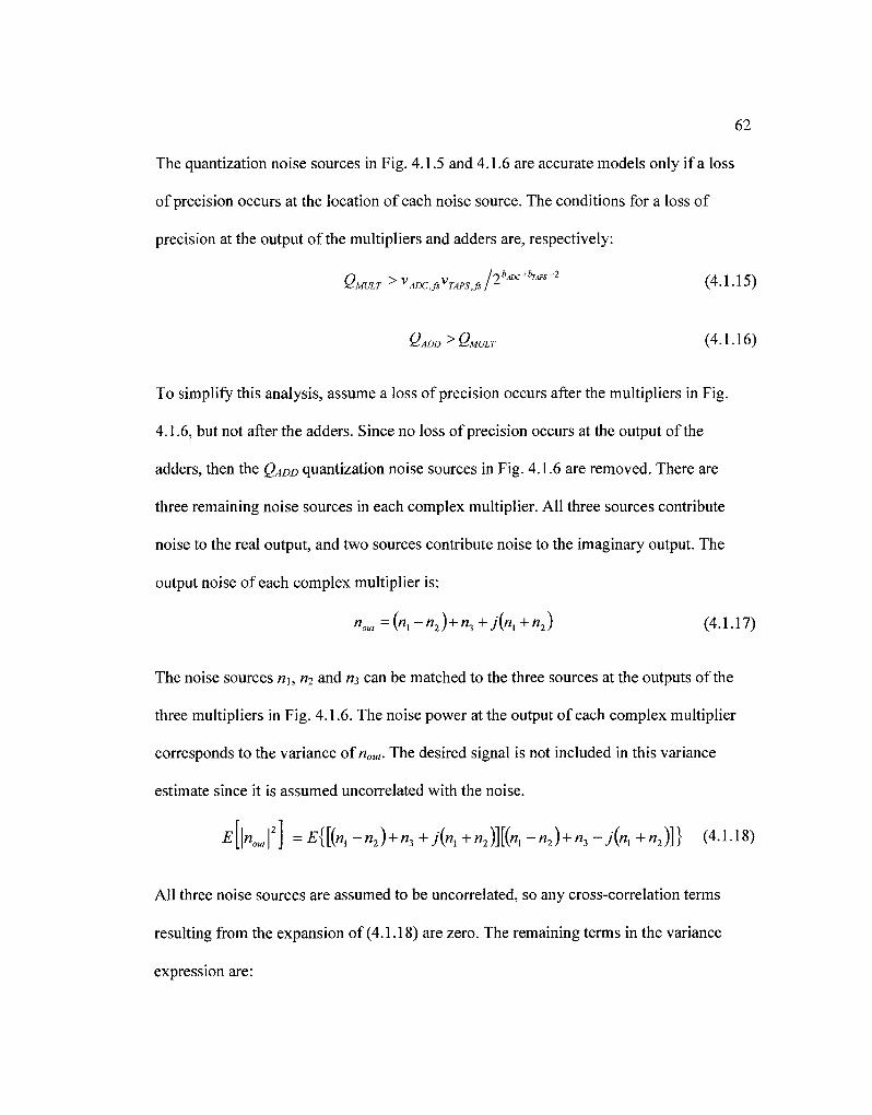
62
The quantization noise sources in Fig. 4.1.5 and 4.1.6 are accurate models only if a loss
of precision occurs at the location of each noise source. The conditions for a loss of
precision at the output of the multipliers and adders are, respectively:
QMULT >vADcjsvTAPsjJlbADC+bTArs-2 (4.1.15)
QADD>QMULT (4.1.16)
To simplify this analysis, assume a loss of precision occurs after the multipliers in Fig.
4.1.6, but not after the adders. Since no loss of precision occurs at the output of the
adders, then the QADD quantization noise sources in Fig. 4.1.6 are removed. There are
three remaining noise sources in each complex multiplier. All three sources contribute
noise to the real output, and two sources contribute noise to the imaginary output. The
output noise of each complex multiplier is:
nout =("i - « 2 ) + " 3 +X"i +ni) (4.1.17)
The noise sources n\, n2 and «3 can be matched to the three sources at the outputs of the
three multipliers in Fig. 4.1.6. The noise power at the output of each complex multiplier
corresponds to the variance ofnout. The desired signal is not included in this variance
estimate since it is assumed uncorrected with the noise.
= £{[(«! -n2) + n3 +j(n1 +n2)][(nl -n2) + n3 -y(w, +n2)]} (4.1.18)
All three noise sources are assumed to be uncorrected, so any cross-correlation terms
resulting from the expansion of (4.1.18) are zero. The remaining terms in the variance
expression are:
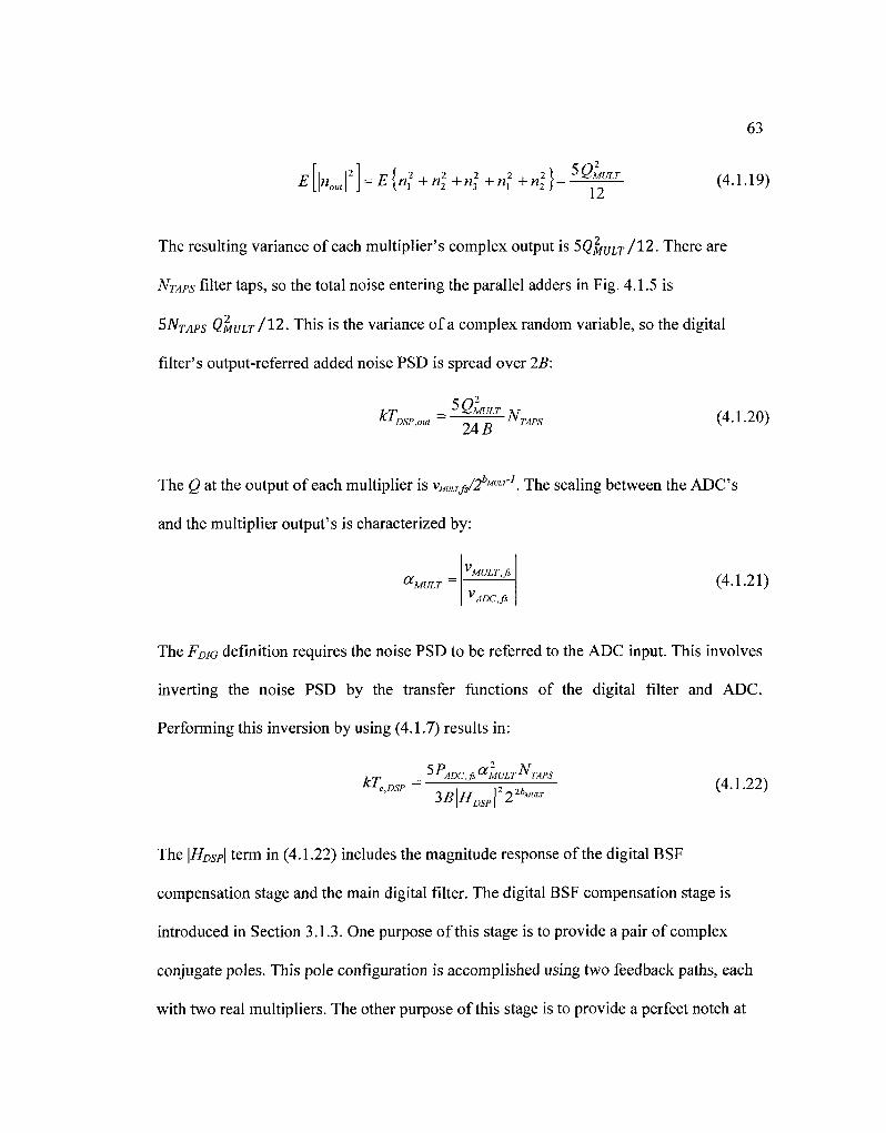
63
= E{n2x +n2
2 +nl +n2 + » 22 } = 5 g ^ r (4.1.19)
The resulting variance of each multiplier's complex output is 5QMULT/12. There are
NTAPS filter taps, so the total noise entering the parallel adders in Fig. 4.1.5 is
5NTAPS QMULT/12. This is the variance of a complex random variable, so the digital
filter's output-referred added noise PSD is spread over 2B:
kTDSP,oul-^f^NTAPS (4.1.20)
The Q at the output of each multiplier is vMUUFjJ2hMULrl. The scaling between the ADC's
and the multiplier output's is characterized by:
Al JT T /"r.
(4.1.21) aMULT
VMULT,fs
VADC,fs
The FDIG definition requires the noise PSD to be referred to the ADC input. This involves
inverting the noise PSD by the transfer functions of the digital filter and ADC.
Performing this inversion by using (4.1.7) results in:
IrT - ADC-fS MULT TAPS (A 1 -,-IX K1e,DSP ~ i a~Th (4.1./Z)
3B\HDSP\22bua'
The \HDSP\ term in (4.1.22) includes the magnitude response of the digital BSF
compensation stage and the main digital filter. The digital BSF compensation stage is
introduced in Section 3.1.3. One purpose of this stage is to provide a pair of complex
conjugate poles. This pole configuration is accomplished using two feedback paths, each
with two real multipliers. The other purpose of this stage is to provide a perfect notch at
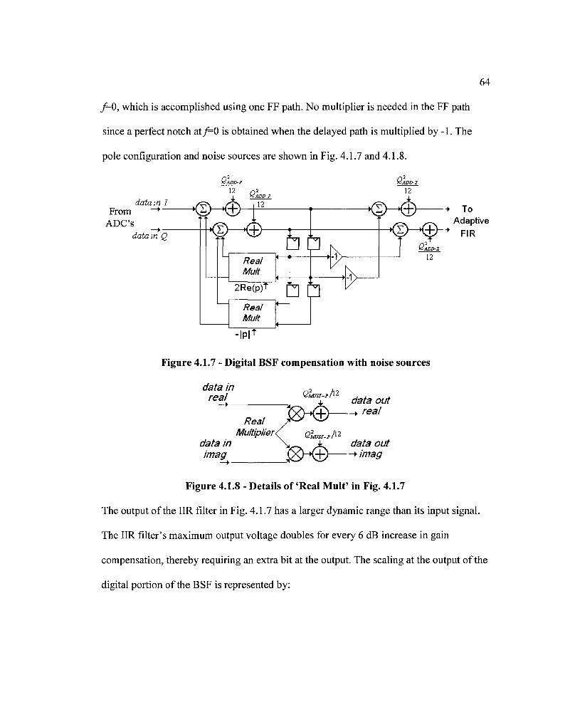
64
f=0, which is accomplished using one FF path. No multiplier is needed in the FF path
since a perfect notch atf=0 is obtained when the delayed path is multiplied by -1. The
pole configuration and noise sources are shown in Fig. 4.1.7 and 4.1.8.
QADD-P QA.
data in I /^\ /f\ ,12
From <£H©—f~
2ADD-Z
12
ADC's data in Q <§)—®—r
Real Mult
2Re(p)T
/tea/
+ To Adaptive
QALD-Z
12
• | p | T
Figure 4.1.7 - Digital BSF compensation with noise sources
data in real
— • —
data in imag
Real Multiplier
4> P /12
QMIIT-P / ' '
data out _• real
i d, imag
Figure 4.1.8 - Details of 'Real Mult' in Fig. 4.1.7
The output of the IIR filter in Fig. 4.1.7 has a larger dynamic range than its input signal.
The IIR filter's maximum output voltage doubles for every 6 dB increase in gain
compensation, thereby requiring an extra bit at the output. The scaling at the output of the
digital portion of the BSF is represented by:
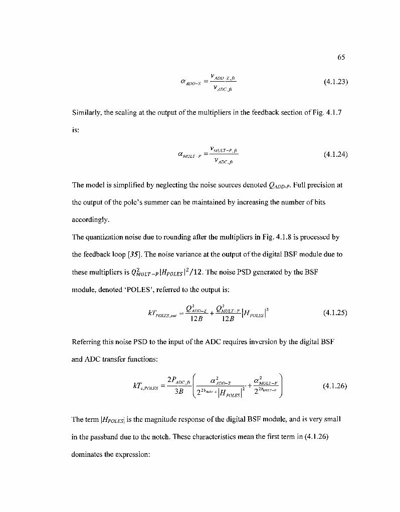
65
VADD-Z,fs aADD-z= — (4.1.23) VADC,fs
Similarly, the scaling at the output of the multipliers in the feedback section of Fig. 4.1.7
i s :
VMULT-P,fs . , , _ ..
<XMULT-P = — (4.1.24) V ADC.fi
The model is simplified by neglecting the noise sources denoted QADD-P- Full precision at
the output of the pole's summer can be maintained by increasing the number of bits
accordingly.
The quantization noise due to rounding after the multipliers in Fig. 4.1.8 is processed by
the feedback loop [35]. The noise variance at the output of the digital BSF module due to
these multipliers is QMULT-P WPOLES l 2 /12. The noise PSD generated by the BSF
module, denoted 'POLES', referred to the output is:
IrT - QADD-Z I QMULT-P I r_r I2 (A I 7«\ ' " POLES, out ~ 1 0 D "•" , - „ I -" POLES | \~t.i..*.J)
Referring this noise PSD to the input of the ADC requires inversion by the digital BSF
and ADC transfer functions:
f \ IP
rrp _ /L1 ADC,fa K-L e,POLES ~ - , „
a2 a2
" ADD-Z _ , ^MULT-P 0 2bADD-Z I ZJ _
V I POLES] )
(4.1.26)
The term \HPOLES\ is the magnitude response of the digital BSF module, and is very small
in the passband due to the notch. These characteristics mean the first term in (4.1.26)
dominates the expression:
66
IP IrT ~ ^Cfi
a 1 e,POLES
ADD-Z
D-z\H
(4.1.27) POLES
The effective input-referred noise PSD of the ADC's (4.1.8), DAC's (4.1.11) and digital
filter (4.1.22) & (4.1.27) have been derived. These terms are combined to get an
expression for the total digital noise factor:
FD,G=1 + "*e,ADC + ^ e , D A C + *"* e,DSP "*" " ^ e,POLES
kTn
Fmrz = ! + • ADC.fi
kT0B ar
SNRADC SNRn4C\H. DAC\** DSP\
•> •**TAPS a MULT
J \ n DSP /-
2or
3LffB 2 - 2 * .
? | 2 2
(4.1.28)
Equation (4.1.28) is the derived noise factor for the digital components. This noise factor
corresponds to FDIG in Fig. 4.1.2.
4.1.4 Noise Expression Discussion
The goal of the above analyses is to derive the total noise PSD at the hybrid RF-DSP FF
filter output. The total output noise PSD is given in (4.1.1), and the expressions for FRF\,
FDIG, FRFI in (4.1.2), (4.1.28), and (4.1.3), respectively. In this section the output noise
floor expressions are manipulated and simplified with assumptions to answer the
following two questions:
1. Is a sub 1 dB noise figure feasible?
2. Under what conditions does the output noise floor degrade attenuation
performance?
67
The following section reviews the simulations used to verify the noise expression.
1. Is a sub 1 dB noise figure feasible?
A small noise figure is necessary for a receiver application, especially if the entire filter is
placed before the receiver's LNA. In this application the RF FF path is a low-loss
transmission line. The noise factor of the hybrid RF-DSP FF filter is a function of the
output noise PSD from (4.1.1), and the magnitude response of the filter, \HFF\:
FFF(f) = - kTFFfiM
K1 0 K 3 FF\
\HC ' VTOP V
HT0PHC2lHcy
He
+FD ** RFX1* DIG** RF I™ BSF-™C2c**C31
+ t e « - i )
+(^2-0
Hs
" DIG-"RFl" BSF'•"C2c""C3t
Hc
" RF21*BSF**C2c**C3t
He + (*W-i) • " B S F * * C l c 1 * C 3 I
Ht
(4.1.29)
The following assumptions are made to simplify this noise factor expression:
• Top path contains a passive component: FTOP=\HTOP\~2
• The RF BSF is RLC based (ie. passive): FBSP=\HBSF\~2
• The RF FF path dominates the transfer function of the total filter in the passband
\HFF(fp)\~\Hc\tHTOp(fp) HC2t HC3t |
Under these assumptions the noise factor expression from (4.1.29) reduces to (4.1.30) in
the passband.

68
Fffifp)-- • +
\" Clf™ TOP™ C2f™ C3t\
HC2c
"C\t™ TOP™ C2t \\™TOP\ H, cu\
" BSF ™ C2c
"c\t " TOP "C2l f RF\ - " RF\ " DIG"- RF2
+\FD1G ~ V\H D1GHRF2 | + \FRF2 ~ O p RF2 \ ~ l
(4.1.30)
The thru port magnitude responses of the couplers account for power transferred to the
coupled port and power dissipated within the coupler. Wideband directional couplers
from e-MECA exhibit a maximum of 0.1 dB dissipative loss with 10, 20 and 30 dB
coupling factors [36]. A dual-directional coupler provides a low loss combined solution
for CI and C2. One such coupler is available from e-MECA with 0.1 dB of dissipative
loss [37], which is equivalent to CI and C2 each exhibiting 0.05 dB of dissipative loss,
and \HTOP\=1- These insertion loss values are used to replace the thru port magnitude
responses of the couplers with:
//cu |2=io-^°(i-|//c l c |2)
//C2(|2=io-005^(i-|//C2c|
2)
(H"c,r) (4.1.31)
#C3, = 1 0 -0 1/10
The sum of the first two terms in (4.1.30) is shown in Fig. 4.1.9 for various directional
coupler configurations using the relationships in (4.1.31). Since a dual-directional coupler
configuration is assumed for the implementation of CI and C2, their coupling factors are
equal: \HC\c\=\Hc2c\- The horizontal axis is the noise factor contribution for the indicated
coupler configuration. As an example, the configuration consisting of CI, C2 and C3
69
having coupling factors of 20, 20 and 10 dB, respectively, is labelled 20,20,10, and has a
noise factor contribution equal to 1.198.
30 30 20
20 20 20
20 20 10
30 30 30 •
20 20 30
30 30 10
10 10 20
10 10 10
10 10 30 «
1.1 1.2 1.3 1.4 1.5 Noise factor contribution from first two terms in (4.4.29)
1.6
Figure 4.1.9 - Noise factor contribution from first two terms in (4.1.30) for various
couplers
A sub 1 dB noise figure requires: Fpp(fp)<l.26, which means the contribution from just
the first two terms in (4.1.30) should be much less than this value. There are several four
coupler configurations in Fig. 4.1.9 with a noise factor contribution between 1.05 and
1.09. Using one of these four configurations limits the remainder of the terms in (4.1.30)
to between 0.17 and 0.21 to achieve a sub 1 dB noise figure. The remainder of the terms
are manipulated to determine what conditions are necessary for them to equal between
0.17 and 0.21. The third term in (4.1.30) is neglected since \HTOP\2=l for a dual
directional coupler.
The combined response of the digital filter and RF BSF within the passband relative to an
interferer occupied frequency (fmt) is defined as:

70
AH DIG Vp J^BSF Vp ) - 77 If \TT T}~\ - " DIG V/rnt / • " BSF Vin t /
The magnitude response of the digital filter and RF BSF at/„, must result in FF
attenuation; therefore can be expressed in terms of the other components.
\"cu"TOP"-C2t\ = \"cic^'RFl^'DIG\Jmt)^RF2-"BSF\Jmt)^:'C2c\
•"• | HD1G (/mt )HBSF 1/rnt ) | = "c\t **TOP **C2t
** Clc-™ RF1-™ RF2** C2c
(4.1.32)
(4.1.33)
The purpose of introducing a new term in (4.1.32) is to replace the \HADC\ and \HDAc\
terms, since they contain a multitude of design variables. These terms are replaced with
the ratio of the digital filter and RF BSF responses in the passband to that at^,. The
magnitude response of the digital components and RF BSF in the passband becomes:
HDIG (fp )HBSF [fp ) = AHD1G (fp )AHBSF (fp ) **CU**TOp"c2t
• "Clc™RF\**RF2**C2c
(4.1.34)
The ratio of the BSF attenuation within the passband to that at the nearest attenuation
frequency outside the passband, AHsspifp),IS assumed to be -10 dB. This assumption is
based on 20 dB of BSF attenuation in the passband, and the first stopbands starting where
the BSF exhibits 10 dB of attenuation.
The terms from the last two lines of (4.1.30) are shown below, but with the substitution
from (4.1.34):
71
RF\ ~lFF\BOT\fp) ^1
+ ( ^ 2 - 1 )
&HD1G(fp)AHBSF(fp)
H, cu + ( ^ / G - l )
AHDlG(fp)AHBSF(fp)
"c\c " RF\
"RF2 "BSF \fp ) " C2c
"cu -"TOP "cit
" BSF" C2c
"cu "TOP "C21
(4.1.35)
The full-scale analog power levels of the ADC's and DAC's are related to the maximum
RF input power of the hybrid RF-DSP FF filter. The input power to the hybrid RF-DSP
FF filter that causes a full-scale digital output from the ADC's is denoted by PFFJS- The
DAC full-scale power should be large enough to attenuate a signal in the RF path with
power PFFJS outside of the passband. The relationships between these full-scale power
levels are given by (4.1.36). The HBsF,mm(fmd term in this equation represents the
minimum gain of the RF BSF outside the passband.
"ADC./S "FFJS\"CIC"RFI\
p = p 1 FFJs x DACJs
"C2c " RF2 " BSF mm if J "C\l"TOP"C2i
Substituting these equations into (4.1.35) to remove HRF\ and HRFI yields:
W=*Wi AHD1G(fp)AHBSF(fp)
r FF\BOT\J p) rRF\ JJ HClc
+{FD1G -\)^^\MjD1G{fp)^nBSF{fp)\
+ ( ^ 2 - l ) -FFJs
"DACJS
H ' (f) BSF V p J
H BSF,mm (fj " BSF" C2c
"Clt" TOP" I TOP"C2t
(4.1.36)
(4.1.37)
There are four terms in (4.1.37) that must sum to 0.17 or less to achieve a sub 1 dB noise
figure. The maximum input interferer power for this analysis is set to -15 dBm, which
corresponds to the maximum blocker power in the WCDMA standard[5#]. Each of the
72
four terms is discussed individually. The goal of the noise factor contributions from the
first three terms in (4.1.37) are 0.01, 0.15 and 0.01, respectively.
The first term contains the coupling factor of CI in the denominator, which removes the
possibility of using a 30 dB coupling factor. A trade-off between this term and the results
from Fig. 4.1.9 indicate that CI should have a 20 dB coupling factor. This coupling
reduces the range of values for the terms in (4.1.37) to between 0.17 and 0.18, depending
on whether C3 is a 20 or 30 dB coupler, respectively. The value of FRF\ corresponds to a
direct-down conversion receiver, which can be on the order of 2 dB. For the first term in
(4.1.37) to be less than 0.01, with FRFX= 2 dB, and \HC\C\= -20 dB, then
\AHDjG(fp)AHBSf{fp)\< -42 dB. As previously stated, the minimum value of AHBsFifP) is
assumed to be -10 dB, so the digital filter needs to provide some notches for the
additional 32 dB over the passband.
The second term in (4.1.37) is the noise factor contribution from the digital components,
which includes the noise factor of the digital components from (4.1.28). The digital noise
terms due to rounding after the multipliers and after the IIR stage are dropped from
(4.1.28). In a low noise implementation these noise sources can be insignificant if no loss
of precision occurs until the data reaches the DAC's. Substituting the digital noise factor
into the second term in (4.1.37), and applying the digital precision assumptions yields:
\WDIG{fp)AHBSF(fp)\2 \aDACAHD1G(fp)AHBSF(fp)\
2
F (f )= PpFJs
rFF\D,GVp) k T B 0-" SNRADC SNRDAC\HDSP(fp)\2
(4.1.38)
The value of \tS.HDIG(fp) MlBsF(fp)\ in (4.1.38) has already been constrained to be less than
-42 dB, due to the first term in (4.1.37), and the full-scale power at the RF input is -15
73
dBm. If the digital clock frequency is 200 MHz, then the noise factor contribution from
the first term in (4.1.38) is 0.001 when SNRADC>67 dB. The second addend in (4.1.38) is
due to the DAC and is simplified using (4.1.32):
=W=-"FFJS 1 FF.fi
FF\OACVP, kToB]SNRDAC
"mc^BSpifp)
"DSpUint) (4.1.39)
The ratio of the DAC full-scale value to the ADC-full scale value (aDAc) should be on the
same order as the maximum gain of the digital filter at the interferer occupied frequencies
\HDSP,max(fint)\- This minimum limit on aDAC is required to avoid saturation. If this ratio is
larger than \HDSp,max(fmdl then there is wasted overhead in the digital filter that will
increase the noise figure. The frequencies where HDsp(fmt) is maximum correspond to the
nearest frequencies to the passband where attenuation is required. This maximum
corresponds to the frequencies where the digital filter provides the most gain to
compensate for the wide attenuation bandwidth of the RF BSF. The result of this
discussion is that aDAC~\HDSPimax(fm,)\.
Under the assumptions presented above, the value of SNRDAc must be greater than 77 dB
for the expression in (4.1.39) to be less than 0.15. This value of SNRDAc requires a DAC
with an effective number of bits (ENOB) equal to 12.5.
The third term in (4.1.37) is due to the noise generated within the RFl components. With
a -15 dBm full-scale RF input to the hybrid RF-DSP FF filter, the remaining terms
require (FRF2-\)IPDAC,FS<3-\6 to ensure the entire third term is less than 0.01. The DAC
used in the hardware prototype has PDACFS^W dBm [39], which would limit FRFI to be
74
less than 31.2, which corresponds to a 14.9 dB noise figure. This noise figure
specification is realistic for a cascaded modulator and amplifier .
The fourth term in (4.1.37) is negligible, and can be ignored without concern since it is
negative and would only reduce the noise factor.
This analysis has laid out one set of conditions required for a sub 1 dB noise figure. The
most stringent specification is for the DAC SNR. These conditions are feasible; therefore
the hybrid RF-DSP FF filter can be designed to exhibit a 1 dB noise figure.
2. Under -what conditions does the output noise
floor degrade attenuation performance?
If the output noise floor is larger than the interferer PSD after attenuation, then the noise
would appear to degrade the attenuation. The output noise PSD at interferer frequencies
is obtained from (4.1.1), where/is substituted with/„,. Several approximations are made
to simplify this expression at frequencies occupied by interferers (fmt):
• The magnitude response of the top and bottom paths are equal at interferer
locations: \Hc\tHTOpHc2t\=\Hc\cHRF\HDiG{fim)HRFiHBSF (fmt)Hc2c\-
• The top path is a lossless passive component: FTOP=\HTOP\ = 1 .
• Any terms in (4.1.1) that are expected to be near the noise floor are ignored.
These include the first and last lines of (4.1.1). The justification for dropping
these terms is that the filter is designed to attenuate strong interferers by 10's of
decibels, which is expected to be well above the thermal noise floor.
The output noise PSD within interference bands, subject to the above approximations, is
given by:
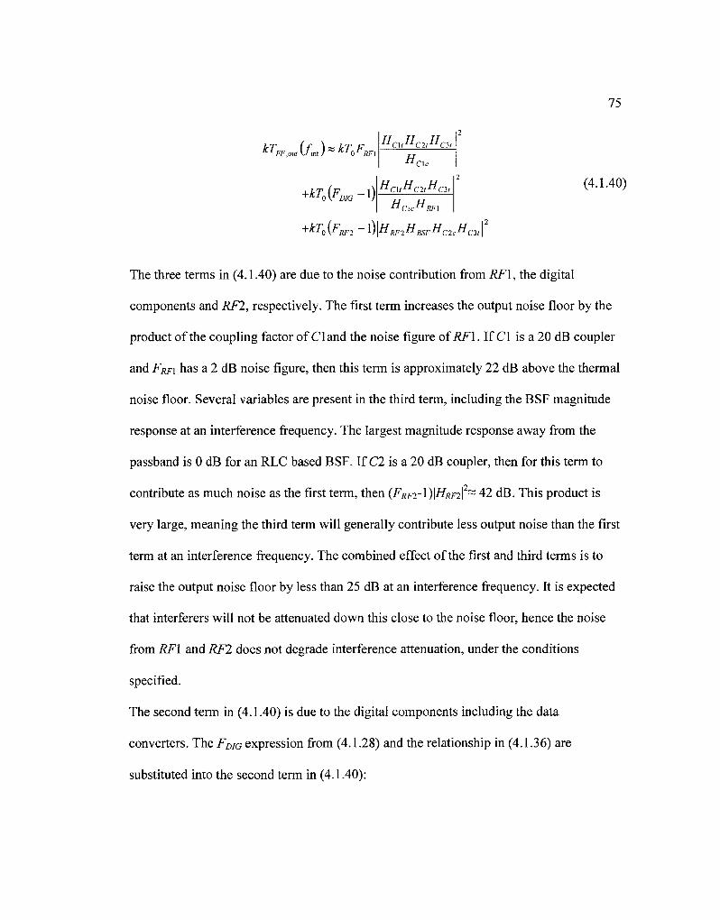
75
kTFF,ml{fJ*kT»F> RFl
2
"•CM "c2l^C3t
+kT0{FD!G~l)
Hcu 2
• " c i > " c 2 / "at
"C\C"RF\
(4.1.40)
+kT0(FRF2 -V^H^HespHc^H, 2
C3t\
The three terms in (4.1.40) are due to the noise contribution from RFl, the digital
components and RFl, respectively. The first term increases the output noise floor by the
product of the coupling factor of CI and the noise figure of RFl. If CI is a 20 dB coupler
and FRFI has a 2 dB noise figure, then this term is approximately 22 dB above the thermal
noise floor. Several variables are present in the third term, including the BSF magnitude
response at an interference frequency. The largest magnitude response away from the
passband is 0 dB for an RLC based BSF. If C2 is a 20 dB coupler, then for this term to
contribute as much noise as the first term, then (FRF2-1)\HRF2\2~ 42 dB. This product is
very large, meaning the third term will generally contribute less output noise than the first
term at an interference frequency. The combined effect of the first and third terms is to
raise the output noise floor by less than 25 dB at an interference frequency. It is expected
that interferers will not be attenuated down this close to the noise floor, hence the noise
from RFl and RF2 does not degrade interference attenuation, under the conditions
specified.
The second term in (4.1.40) is due to the digital components including the data
converters. The FDIG expression from (4.1.28) and the relationship in (4.1.36) are
substituted into the second term in (4.1.40):
1 FF,out\DlG V/int / n
f , DAC kT (f )= FFJi
FF.out\DlG V mt /
1 a2
SNRADC SNRDAC\HDSP(fJ\
Jlyu-MULT _ , ^ " ADD-Z
3\HDSP(fJ\ 2 2 W 3\HPOLES(fJ\ 2 ADD-Z
76
(4.1.41)
y
The thru port magnitude responses of the directional couplers are omitted in (4.1.41) due
to their negligible impact. Consider the case where the FF filter input power is -15 dBm
and the digital clock runs at 200 MHz (5=100 MHz). The multiplication factor in front of
(4.1.41) for this scenario is -95 dBm/Hz. Each addend in (4.1.41) reduces this factor by
an amount that depends on the digital design variables. To ensure the noise generated by
the ADC causes the noise floor to rise only 22 dB above the thermal noise floor, then:
SNRADC>57 dB. The same constraint exists for SNRDAc when aDAc~\HDSP(fm,)\. The 57 dB
limit on the SNR's corresponds to an ENOB of 9.2, which is achievable. The other two
terms in (4.1.41) can be negligible be ensuring adequate scaling and bit widths
throughout the digital filter.
This section has shown that noise generated by the lower FF branch can be less than 30
dB above the noise floor over interferer occupied bands without requiring exotic
components. This noise floor means that interferers can be attenuated down to 30 dB
above the noise floor before the added noise appears to degrade the attenuation
performance.
4.1.5 Simulation for Verification of FDIG
Most of the RF noise analysis in the previous sections is straight from an undergraduate
textbook. Digital components are not generally incorporated into an RF noise analysis.
77
Consequently, simulations were performed to validate the analysis using Simulink. The
digital filter in Simulink includes fixed-point settings, which permits truncation, rounding
or scaling after arithmetic operations. Fig. 4.1.10 and 4.1.11 show the model used in
Simulink.
eps+U'eps- •
Null start
Noise Temperature -
54510794.6051
Wideband Noise
Remove all passband
noise
Highpass - • Temperature —•^ [ I npu t ] | 290 K
[pnput] > — ^ Lowpass - >\ Pin |
Receiver Thermal Noise
extract passband
only
coupl
Digital filter stuff
LPF Anti-alias
HRF1 FRF2 reconstruction Noise I r ^ v . IFDATot I Noise I f \ . iFDATol I Noise Figure- • H r f 1 > * \ • In Out > • Figure- • H r f 2 > ^ \ • Figure-OdB l ^ ^ | If | 0 dB [ \ y ^ \ If 20 dB
coupl
out • Lowpass - WPout
extract passband
onlyl
Fbsf Hbsf
Figure 4.1.10 - Simulink model for digital noise analysis
Latency
CT>| In
-19 Noise
Temperature^ OK #
ADC
Digital Filter
ADCNoise Q U 3 n t ' Z e r Digital BSF AUCNoise pre-Comp
myWindow #
Num
Digital 0 u t
Filter • double
Adaptive FIR and DAC
Convert
Noise Temperature — • ( 1 ~)
OK Out
DAC Thermal f £ e i K Noise Floor to double
FIR coefficients
Tap Quantizer
Figure 4.1.11 - Details of 'Digital filter stuff block from Fig. 4.1.10
The cascade of blocks at the top of Fig. 4.1.10 generate the filter's input signal. This
input signal has a PSD 66 dB above kT0 outside the passband, and is equal to kT0 within
the passband. The large PSD outside the passband ensures the input signal spans many
quantization levels in the digital components. The RF passband bandwidth is set to 20
MHz (BP=10 MHz at baseband).
The following fixed component values were used in the simulation:

78
• HTOP is a zero-length transmission line (\HTOP\~FTOP=1)-
• C\ and C2 are ideal 20 dB couplers.
• HRFI and HRF2 provide 20 dB of gain, and have noise factors FRFJ-0 dB, and FRJ?2~0
dB (except in last row in Table 4.1). These blocks are labelled in Fig. 4.1.10.
• HBSF provides 20 dB of attenuation over the passband. The BSF is implemented
with a 20 dB attenuator, along with a noise figure block.
• The digital clock frequency is 200 MHz (5=100 MHz).
• Anti-alias and reconstruction filters bookend the digital filter, each with a 100 MHz
bandwidth.
• The FIR part of the digital filter has 32 randomized taps. The average magnitude-
squared response of\HDsp\ in the passband, including that of the digital BSF
compensation module is defined as: \HDSP | = J_J WDSP I2 df /2Bp.
• The DIG BSF compensation is setup to provide a maximum of 9 dB of dynamic
range increase at ±15 MHz. This compensation corresponds to a maximum gain in
the DIG BSF module of 6 dB, and requires poles at z=0.7e±j0 3.
• The magnitude response of the ADC's is set so that an input voltage level of 1
corresponds to a digital word value of 1. The DAC's adhere to the same 1:1
relationship. These result in: \HADC\=\HDAC\=^ •
• The following digital word full-scale ratios were used throughout these simulations:
O-DACT-22, aMuLT^-'X, & o.ADD.z=\. These values were chosen to optimize digital
resources while avoiding saturation.
79
The input and output noise in the passband are recorded by the blocks on the far right in
Fig. 4.1.10. This data is then processed by (4.1.42) to extract the simulated noise factor
(Fsim)- The terms S,„(f) and Soutif) are the PSD's of the input and output signals. These are
obtained by processing the recorded data with a built-in Matlab FFT averaging function.
The parameter FSIM is the noise factor averaged over the passband.
J _ f S0Ul{f)l\HFF{f)\ ^=^p"'T7;r'^ ^
The noise factor for the hybrid RF-DSP FF filter is defined in (4.1.30) with a passive
component in the top path. This equation requires FDIG from (4.1.28). The noise factor in
(4.1.30) is expressed as a function of frequency, so this expression is averaged over the
passband to obtain a result that is comparable with the simulation results:
1 f°+BP
F™>=TT \FFF{f)df (4.1.43) l t P h-B,
FSIM and FEXP are shown for several filter realizations in Table 4.1. The filter realizations
differ in the digital components details. In the last row of the table the noise figures of the
RF\ and RF2 modules are both changed from 0 to 6 dB.
80
Table 4.1 - Noise simulation results for varying digital resources
(dB) -0.30 3.97
2.101 4.893 4.2 -35.93 -1.857
ADC
SNR(dB) 70 194 194 194 70 70 70
Bits 12 32 32 32 12 12 12
DAC
SNR(dB) 194 70 194 194 83 83 83
Bits 32 12 32 32 14 14 14
FIR MULT
Bits 32 32 12 32 18 18 18
Digital BSF
Bits 32 32 32 12 14 14 14
FSIM
2.0355 4.5340 5.1975 6.0154 3.814 1.0866 3.8927
FEXP
1.9918 4.5095 5.4026 5.9683 3.7814 1.0848 3.9182
The simulation and theoretical results are very close for these seven realizations. The
derived expressions can be used to ensure efficient resource allocation of the digital
components. These equations provide closed-form relationships between noise
performance metrics and design parameters.
4.2 Feedforward Attenuation Analysis
FF techniques involve the cancellation of two signals that come from two different paths.
Attenuation in a FF system degrades as amplitude or phase mismatches increase between
the two paths. Three causes of mismatch are:
• finite-precision representation of the filter tap coefficients
• group delay mismatch between the two signal paths caused primarily by the
latency inherent to the digital components,
• steady-state error associated with the adaptive algorithm that drives the digital
filter's tap coefficients.
81
The attenuation degradation due to the first two points are derived in this chapter. The
focus of the following chapter is the adaptive algorithms for the hybrid FF filter. Suitably,
the degradation due to the third point is deferred to the following chapter.
4.2.1 Filter Tap Quantization
Consider a set of digital filter coefficients that result in perfect FF cancellation at several
frequencies for the hybrid RF-DSP FF filter. The depth of these perfect notches will
degrade when the digital filter coefficients are represented by fixed-point values. The
degradation will be continually changing since the digital filter is adaptive. A statistical
analysis relating FF attenuation to filter tap quantization step-size (QTAPS) is attached as
Appendix A. This step-size is a function of the number of bits (bjAPs) used to represent
the real and imaginary components of the digital filter taps. The step-size also depends on
the maximum digital value used in the fixed-point representation (v^ps^-This value is
the maximum value for the real and imaginary components of the tap coefficient that can
be represented without saturation or wrap-around.
VTAPS 2bTAPS-i (HU..I)
The statistical analysis follows that in [33] for a direct-form digital filter. The result of
this analysis is an upper limit on QTAPS such that FF attenuation will be better than
\HFF,des(G>mt)\ for 99.97% of the time. The upper bound is given by (4.2.2). In this
equation, NJAPS is the number of filter taps.

82
^ ^ • 3 # / * - , * , faint) . . - - . &™s ^ m i n , — •„ „—~ ~ ~—7 \7T~\ ^4-2-2)
"W \4-lVTAps \HC\cHRF\HADCHDACHRF2HBSF\COmt)HC lC2c\
The inequality in (4.2.2) is rearranged using (4.2) to isolate the number of tap bits:
z. ^ 1 V - ' TAPS ' " c i e - " S F l " ADc"DAC™ RF2**BSpV^mt ) " C2c\VTAPS,fs . , „ „N
*/^s 5: log2 ! r - 7 r, ! ^ (4.2.3)
| ^ F F , ^ f a m , ) |
The following relationships are extracted from (4.2.3):
• Every time the number of taps (NTAPS) is doubled, brAPs must be increased by half
a bit to maintain the same FF attenuation.
• An increase in the desired FF attenuation, \HFFcles(a)mt)\, by 3 dB must be
accompanied by an increase of half a bit of bjAPs
• The number of bits is limited by the maximum value of the magnitude response of
the BSF.
This design equation is only valid to determine the limit of FF attenuation degradation
due to coefficient quantization. It is used to verify the hardware prototype has a
sufficiently small tap coefficient quantization step-size to prevent attenuation
degradation. Group delay mismatch also degrades FF attenuation, which is reported next.
4.2.2 Group Delay Mismatch
Group delay mismatch between the paths of a FF system is well known to limit the
attenuation bandwidth. The ADC's, DAC's and DSP have inherent latency due to
pipelining, and filtering. Furthermore, the anti-alias and smoothing filters have finite
group delay, which increases the group delay mismatch between the top and bottom FF

83
paths. The effect of this group delay mismatch is derived in this section. The number of
digital filter taps is not limited in this derivation.
The transfer functions of the RF components in the hybrid FF filter can be represented
with their baseband equivalent functions. The hybrid FF filter block diagram in Fig. 4.2.1
shows the transfer functions in discrete-time. The discrete-time domain is used in this
analysis since this derivation is focused primarily on the digital filter.
x n S.
nJ H TOP
c, fpa—>y[n] n
H RF\ H ADC HDSP(Z) H i l DAC
11 RF2 HBSF{Z) J
Figure 4.2.1 - Linear discrete-time model of hybrid RF-DSP FF filter
When the digital filter is in steady-state, the cascaded blocks in the bottom branch of the
FF filter can be rearranged in the mathematical model without affecting the output signal.
An equivalent block diagram is shown in Fig. 4.2.2.
cH-Q
n H, TOP -m—o'W
H RFl H ADC H DAC H RF2
u[n\ HBSF(Z) > HBSP{Z)
Figure 4.2.2 - Equivalent model to Fig. 4.2.1 when digital filter is in steady-state
In this formulation the coupling ports of the two directional couplers and the blocks in the
bottom branch, excluding the digital filter, are combined into a block denoted H\(z). The
through ports of the directional couplers and the components in the top FF path are
combined into a block denoted /^(z). The compressed block diagram is shown in Fig.
4.2.3. The negative sign on the summation block is convention.
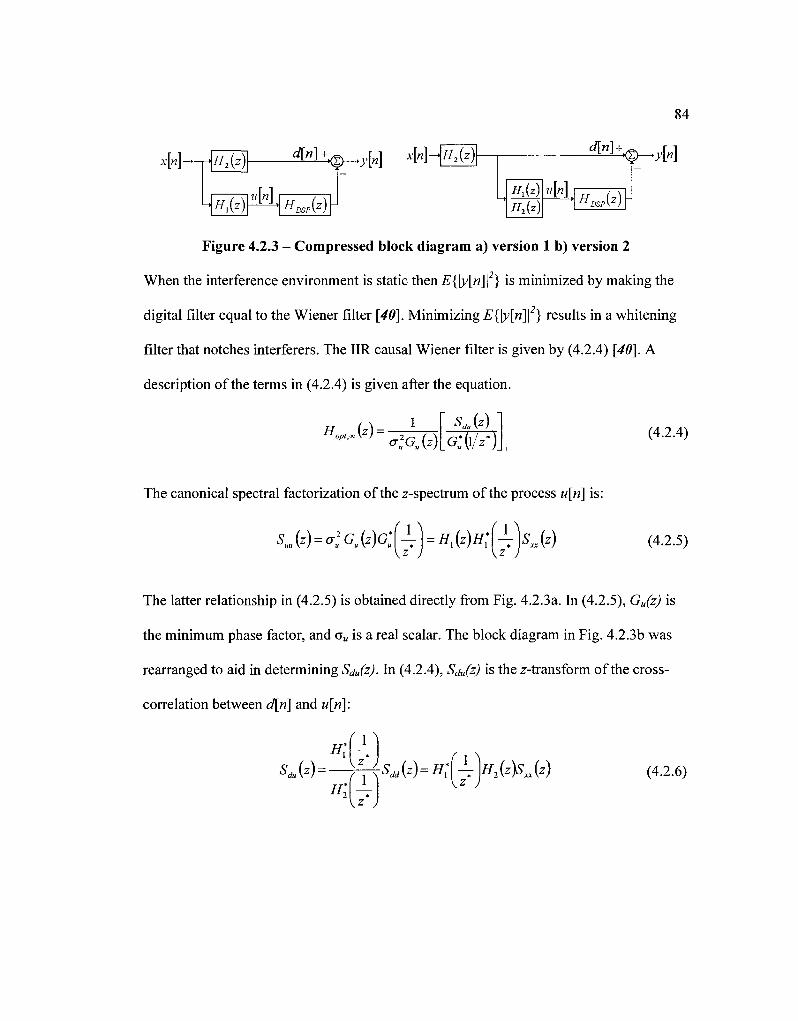
84
U JFM <M+G>_^. [„ ] *MH^E>
!/[«] //,(;) / / _ ( * ) J
- ^ K S ^ M
^ ( z )
H^z)
u[n\ HDSp{Z) J
Figure 4.2.3 - Compressed block diagram a) version 1 b) version 2
When the interference environment is static then ^ [ y M ^ } is minimized by making the
digital filter equal to the Wiener filter [40]. Minimizing .EliyMI2} results in a whitening
filter that notches interferers. The IIR causal Wiener filter is given by (4.2.4) [40]. A
description of the terms in (4.2.4) is given after the equation.
1 HOP,,M=- ^Gu(z)
Sd„(z) (4.2.4)
The canonical spectral factorization of the z-spectrum of the process u[n] is:
Sjz) = al GU{Z)G:(±) = H^H^S^z) \z J \z )
(4.2.5)
The latter relationship in (4.2.5) is obtained directly from Fig. 4.2.3a. In (4.2.5), Gu(z) is
the minimum phase factor, and o„ is a real scalar. The block diagram in Fig. 4.2.3b was
rearranged to aid in determining SdU(z). In (4.2.4), Sdu(z) is the z-transform of the cross-
correlation between d[n] and u[n]:
Sdu{z) = -H; U') K
r 1 \
v ^ J
Sdd{z)=H;(\]H1(z)Sxx(z) Kz J
(4.2.6)

85
The [Q+ operator in (4.2.4) is the causal component of the inverse z-transform. Equation
(4.2.7) shows the proper use of this operator. This operator differs from the one-sided z-
transform, since for said transform h[n]=0 for n<0.
{H{z)}+=ZT{h+[n]} H(z) = ZT{h[n]} (4.2.7)
The expressions in (4.2.5) and (4.2.6) are substituted into (4.2.4) to arrive at the Wiener
filter transfer function.
HoplAz)-
O", IGM
H2(Z)H;\±)S„{Z) ''J v ^ J
G: 'n
a. •IGM
\z )
r 1 A H2{Z)H;\\)J2
UGU{Z)G: \z J
—I \z')
G:\\]HAZ)H;{^ ~z ) \z )
GAz) Gu(z)
H2{z) Hx{z)
(4.2.8)
The next step in this derivation is to decompose the function H2(z)IH\{z) into a minimum
phase component and a nominal delay term:
H2{z)_ »H'2(z) H,(z) H[(z) (4.2.9)
The value of D is the nominal delay from H2(z)/H\(z). This value includes latency and
group delay. The minimum phase component is H2{z)/Hl{z).
The PSD of multiple interferers at the input to a receiver can appear spiky, which is
characteristic of an auto-regressive (AR) process. This spikiness means that

86
Gu {z)H2{z)/H1 (z) is well modeled by an all-pole transfer function. The poles are
denoted byp, for i=\,2...M. A partial fraction expansion (PFE) of Gu(z)H2{z)/H-^iz)
yields:
G^rPjM (4.2.10)
The^ r values are the coefficients from the PFE. The inverse z-transform of this term is:
IZTl 1V1
•{gu*KlKM = Y.AP>[n\ (4.2.11) /=i
Putting the delay term back into the transfer function gives the following inverse z-
transform:
IZT\ H'i(z).
ivi
= (gu*h'2/hD[n]*S[n + D] = "£A,P:+D4n + D] (4.2.12)
The last modification to this term is made by isolating the causal component of the
impulse response:
IZT{ M
= zZAPTDu[n] (4.2.13)
Converting this result back to the z-domain, and using (4.2.10) gives:
= f>f4/(i-A^) '^.MSW H[{z)_
(4.2.14) /=i

87
The LHS of this result is equal to the causal component in (4.2.8). The transfer function
of the optimum Wiener filter is obtained by substituting the result from (4.2.14) back into
(4.2.8).
1 H0PM = -FT\^P-A-I(X-P-Z~1) (4-2-15>
°H \Z) l=\
When HDsp{z)=HoptJyZ), the transfer function of the FF filter in Fig. 4.2.3b is:
±p?Aj(\-plZ-) H M ^ - ^ n ; (4.2.16)
In the z-domain, interference frequencies are located on the unit circle closest to the poles
of the AR model. At the frequency nearest to pole /, |l-p;z!"/|«|l-/>/z,"7|, for/^ /'. This
means that one term will dominate each of the summations in HoptiK>(z) when the poles of
the AR model are not densely clustered. At the frequencies nearest to pole /',
*M'l-^tP<U-[*X (4.2.H) Z A,/\l-P,Z ) \Z )
This transfer function is changed into analog frequency domain, co:
HFF{a)K\-\p\e]{Zp-'oT)D (4.2.18)
This transfer function is identical to that of a conventional RF FF system with a delay
mismatch of TSD. The notch of this system achieves a depth of \-\p,\, and is located at the
same location as the poles of the input signal's AR model. Recall that Ts is the time step
88
in the digital domain, and D is the group delay mismatch between H\(z) and Hiiz) in Fig.
4.2.3a, in terms of clock periods. In other words, D is an integer without units.
The result in (4.2.18) is a very simple expression that relates the maximum attenuation of
the FF filter to the group delay mismatch (D) and the interferer's pole amplitude in the
AR model. The approximation made in (4.2.17) is valid near frequencies occupied by
interferers.
4.2.3 Number of Filter Taps
The interference cancellation expression in the previous section was for an IIR digital
filter, and the corresponding impulse response represents the IIR Wiener solution. The
digital filter within the hybrid RF-DSP FF filter has an N-tap FIR, which nominally
converges towards the N tap FIR causal Wiener solution. The MSE of the FIR filter
converges to that of the IIR solution for a sufficiently large number of FIR taps.
Arbitrarily increasing the number of FIR taps beyond some limit does not guarantee
measurable attenuation improvement. This statement is easier to demonstrate with
measurements than with theory; therefore is deferred to Section 7.3.1.
4.3 Analyses Summary
Analytical expressions have been derived relating the design variables to noise and
attenuation performance metrics. These expressions can be used to choose component
values based on noise and attenuation specifications. These results are valuable to trade
off hardware resources with filter performance, without needing to resort to exhaustive

89
simulations. The results of this chapter are used in Chapter 6 to choose the components
for the hardware prototype.
A linear analysis is used throughout this chapter. This assumption is problematic if the
RF or analog components are sensitive to the amplitude of their input signals, and if this
amplitude is highly dynamic.

5 Algorithm Development
Adaptive algorithms are required to continuously update the digital filter coefficients in a
dynamic interference environment. The digital filter must also be continuously updated to
compensate for RF and analog component drift. Furthermore, the BSF contains a tunable
component that is adaptively controlled to maintain a deep notch in the passband. The
digital filter and adaptive algorithms are implemented in an FPGA, therefore
computational resources are limited. These adaptive algorithms are presented in this
chapter and verified with simulations.
5.1 Filter Optimization Strategy
The purpose of the hybrid RF-DSP FF filter in a receiver application is to attenuate out-
of-band interferers and transmitter leakage. The output of this filter would ideally have a
uniform PSD (white noise) except within the receiver's passband. The filter should have
unity magnitude and a linear phase response in the receiver's passband. A filter that
converts a non-uniform PSD to a uniform PSD is a whitening filter. A plethora of
literature exists to determine the coefficients of the whitening filter, including adaptive
techniques. This literature is in the field of auto-regressive moving average (ARMA)
modeling, and has applications in channel equalization, system identification, spectrum
estimation, linear predictive coding and active noise control.
90

91
A block diagram of a whitening filter is shown in Fig. 5.1.1. In this figure a white noise
process, w[n], with average power <rl, is input to an ARMA model. The transfer
function of this model is: HARMA(z)=H„um(z)IHden(z). The output of the ARMA model is
termed an ARMA process. The PSD of this ARMA process is completely dependent
upon HARMA(z) and aw. The goal of ARMA modeling is to generate a filter to re-whiten
the ARMA process. The sought after whitening filter is the inverse of the ARMA model:
Hwhite{z)=Hden{z)IHnum{z). The only signal that is available to aid in generating this filter is
the ARMA process, x[ri\. The values of the white noise process at the input to the ARMA
model, w[n], are unavailable.
w[»] White noise
HJ?)
„ u\Hmm{z) x[n] HdJz) Hmm(Z)
-> w'[n] White noise i u i v ^ ^ ARMA
process ARMA process Whitening process
model filter
Figure 5.1.1 - ARMA process and whitening filter
The most common type of ARMA modeling is the auto-regressive (AR) case: Hnum{z)=\
[41]. An AR process results from passing white noise through an all-pole filter. The
corresponding whitening filter, Hwhue(z), is then FIR. An example of an AR process is the
signal at the input to a receiver. Interferers are characteristically spiky in the frequency
domain, therefore are modeled well with white noise filtered by an all-pole filter. An
example of this characteristic is illustrated in Fig. 5.1.2. In this figure the AR model is
represented by its pole locations in the z-domain. AR techniques exist that are capable of
determining Hwhlle(z) and aw based only on the AR process [41]. These techniques
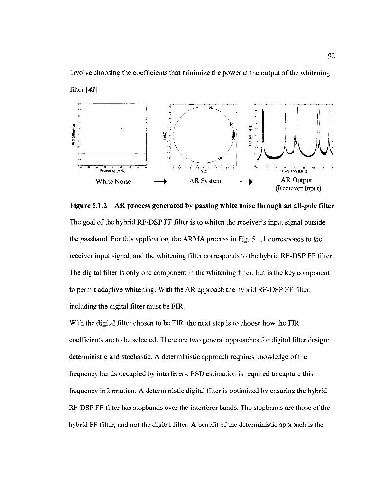
92
involve choosing the coefficients that minimize the power at the output of the whitening
filter [41].
4
,, / -;/
E
";\ -J. x
- . „ . :
\ \
1 /
/ 1 -=^ ..J
s »
: / W U' Frequency (MHz)
White Noise
Re(Z)
AR System
Frequency (MHz)
AR Output (Receiver Input)
Figure 5.1.2 - AR process generated by passing white noise through an all-pole filter
The goal of the hybrid RF-DSP FF filter is to whiten the receiver's input signal outside
the passband. For this application, the ARMA process in Fig. 5.1.1 corresponds to the
receiver input signal, and the whitening filter corresponds to the hybrid RF-DSP FF filter.
The digital filter is only one component in the whitening filter, but is the key component
to permit adaptive whitening. With the AR approach the hybrid RF-DSP FF filter,
including the digital filter must be FIR.
With the digital filter chosen to be FIR, the next step is to choose how the FIR
coefficients are to be selected. There are two general approaches for digital filter design:
deterministic and stochastic. A deterministic approach requires knowledge of the
frequency bands occupied by interferers. PSD estimation is required to capture this
frequency information. A deterministic digital filter is optimized by ensuring the hybrid
RF-DSP FF filter has stopbands over the interferer bands. The stopbands are those of the
hybrid FF filter, and not the digital filter. A benefit of the deterministic approach is the
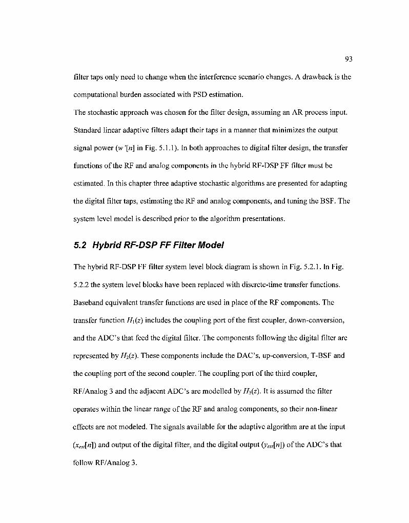
93
filter taps only need to change when the interference scenario changes. A drawback is the
computational burden associated with PSD estimation.
The stochastic approach was chosen for the filter design, assuming an AR process input.
Standard linear adaptive filters adapt their taps in a manner that minimizes the output
signal power (w '[n] in Fig. 5.1.1). In both approaches to digital filter design, the transfer
functions of the RF and analog components in the hybrid RF-DSP FF filter must be
estimated. In this chapter three adaptive stochastic algorithms are presented for adapting
the digital filter taps, estimating the RP and analog components, and tuning the BSF. The
system level model is described prior to the algorithm presentations.
5.2 Hybrid RF-DSP FF Filter Model
The hybrid RF-DSP FF filter system level block diagram is shown in Fig. 5.2.1. In Fig.
5.2.2 the system level blocks have been replaced with discrete-time transfer functions.
Baseband equivalent transfer functions are used in place of the RP components. The
transfer function H\(z) includes the coupling port of the first coupler, down-conversion,
and the ADC's that feed the digital filter. The components following the digital filter are
represented by fyiz). These components include the DAC's, up-conversion, T-BSF and
the coupling port of the second coupler. The coupling port of the third coupler,
RF/Analog 3 and the adjacent ADC's are modelled by H^z). It is assumed the filter
operates within the linear range of the RP and analog components, so their non-linear
effects are not modeled. The signals available for the adaptive algorithm are at the input
(xes,[nj) and output of the digital filter, and the digital output (yest[n\) of the ADC's that
follow RF/Analog 3.
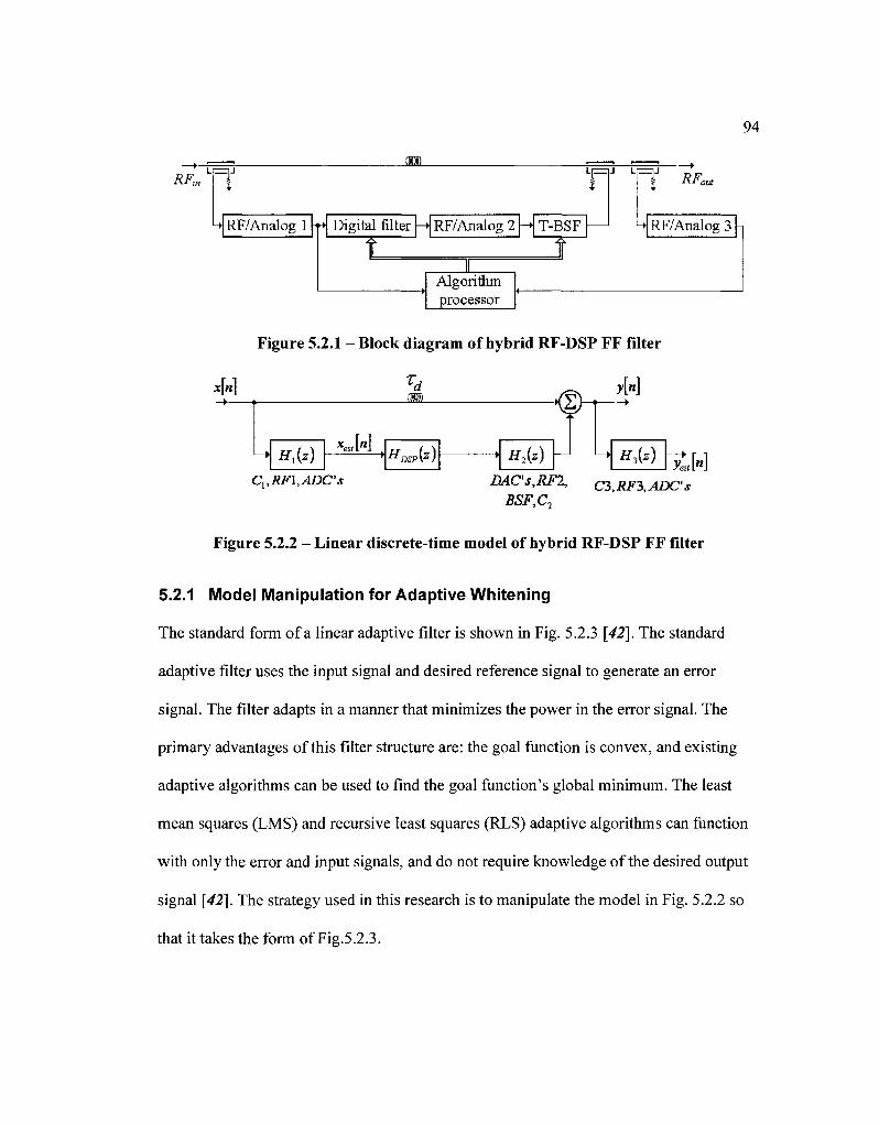
94
RF„ LH" L n J L n J *r-
RF/Analog 1 Digital filter -» RF/Analog 2 -» T-BSF RF/Analog 3 -,
Algorithm processor
Figure 5.2.1 - Block diagram of hybrid RF-DSP FF filter
*M
Cu
Hx{z)
RF\,AD
r i x<An\ .
O's
Mi
•^DSPOO «2W
. ^ rW
H3(z) Vr„
DAC's,RF2, C3,RF3, ADC's BSF,C2
w
Figure 5.2.2 - Linear discrete-time model of hybrid RF-DSP FF filter
5.2.1 Model Manipulation for Adaptive Whitening
The standard form of a linear adaptive filter is shown in Fig. 5.2.3 [42]. The standard
adaptive filter uses the input signal and desired reference signal to generate an error
signal. The filter adapts in a manner that minimizes the power in the error signal. The
primary advantages of this filter structure are: the goal function is convex, and existing
adaptive algorithms can be used to find the goal function's global minimum. The least
mean squares (LMS) and recursive least squares (RLS) adaptive algorithms can function
with only the error and input signals, and do not require knowledge of the desired output
signal [42]. The strategy used in this research is to manipulate the model in Fig. 5.2.2 so
that it takes the form of Fig.5.2.3.
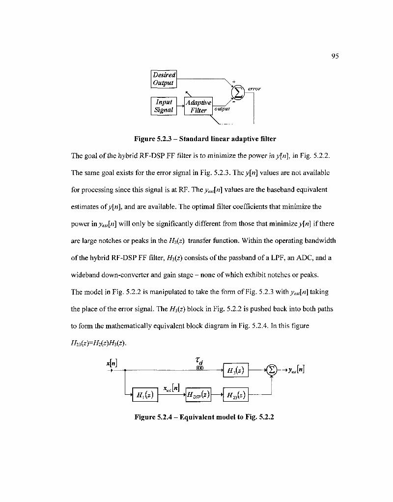
95
Desired Output
Input Signal
\ +
— •
\ Adaptive
Filter
£n output
\
Figure 5.2.3 - Standard linear adaptive filter
The goal of the hybrid RF-DSP FF filter is to minimize the power in >>[w], in Fig. 5.2.2.
The same goal exists for the error signal in Fig. 5.2.3. The^[»] values are not available
for processing since this signal is at RF. T h e ^ M values are the baseband equivalent
estimates of y[n], and are available. The optimal filter coefficients that minimize the
power in>>ej/[«] will only be significantly different from those that minimize y[n] if there
are large notches or peaks in the H3(z) transfer function. Within the operating bandwidth
of the hybrid RF-DSP FF filter, H3{z) consists of the passband of a LPF, an ADC, and a
wideband down-converter and gain stage - none of which exhibit notches or peaks.
The model in Fig. 5.2.2 is manipulated to take the form of Fig. 5.2.3 with.yert[«] taking
the place of the error signal. The H3(z) block in Fig. 5.2.2 is pushed back into both paths
to form the mathematically equivalent block diagram in Fig. 5.2.4. In this figure
H23(z)=H2(z)H3(z).
X[n]
H^z)
xM
(Ml
HDSpiZ)
H,(z)
Hj?)
tfi
7
Figure 5.2.4 - Equivalent model to Fig. 5.2.2
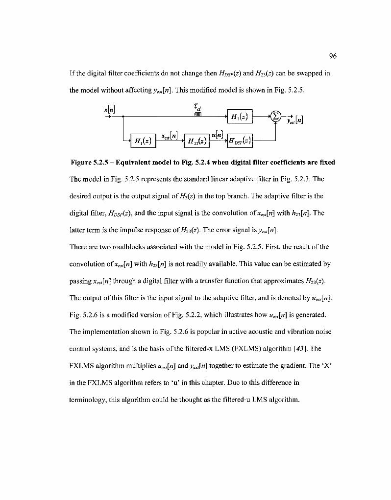
96
If the digital filter coefficients do not change then HDSP{Z) and H?${z) can be swapped in
the model without affecting>W[M]. This modified model is shown in Fig. 5.2.5.
M JUL f ^wJ—^aw
Hx{z) ,M H2k) u[n]
HDSP(2)
Figure 5.2.5 - Equivalent model to Fig. 5.2.4 when digital filter coefficients are fixed
The model in Fig. 5.2.5 represents the standard linear adaptive filter in Fig. 5.2.3. The
desired output is the output signal of H?,{z) in the top branch. The adaptive filter is the
digital filter, HDsp(z), and the input signal is the convolution of xest[n] with hn\ri\. The
latter term is the impulse response of H2?,{z). The error signal is >>„,[«].
There are two roadblocks associated with the model in Fig. 5.2.5. First, the result of the
convolution of xest[n] with h2^[ri\ is not readily available. This value can be estimated by
passing xest[n] through a digital filter with a transfer function that approximates H2i{z).
The output of this filter is the input signal to the adaptive filter, and is denoted by uest[n].
Fig. 5.2.6 is a modified version of Fig. 5.2.2, which illustrates how uest[ri\ is generated.
The implementation shown in Fig. 5.2.6 is popular in active acoustic and vibration noise
control systems, and is the basis of the filtered-x LMS (FXLMS) algorithm [43]. The
FXLMS algorithm multiplies uesl[n] and yest[n] together to estimate the gradient. The 'X'
in the FXLMS algorithm refers to 'u' in this chapter. Due to this difference in
terminology, this algorithm could be thought as the filtered-u LMS algorithm.
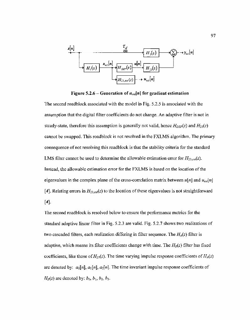
97
*L«J
R,{z) XeAn
m
1 1 HDSp{Z)
u\n\
^-*H2i,est{z)
H3(z)
H23(z)
^
7
- ~* ««»[»]
Figure 5.2.6 - Generation of uest[n] for gradient estimation
The second roadblock associated with the model in Fig. 5.2.5 is associated with the
assumption that the digital filter coefficients do not change. An adaptive filter is not in
steady-state, therefore this assumption is generally not valid, hence HDSP(z) and Hn{z)
cannot be swapped. This roadblock is not resolved in the FXLMS algorithm. The primary
consequence of not resolving this roadblock is that the stability criteria for the standard
LMS filter cannot be used to determine the allowable estimation error for Hn^stiz).
Instead, the allowable estimation error for the FXLMS is based on the location of the
eigenvalues in the complex plane of the cross-correlation matrix between u[n] and uest[n\
[4]. Relating errors in H2-i,est(z) to the location of these eigenvalues is not straightforward
The second roadblock is resolved below to ensure the performance metrics for the
standard adaptive linear filter in Fig. 5.2.3 are valid. Fig. 5.2.7 shows two realizations of
two cascaded filters, each realization differing in filter sequence. The HA(z) filter is
adaptive, which means its filter coefficients change with time. The HB(z) filter has fixed
coefficients, like those of //^(z). The time varying impulse response coefficients of HA{z)
are denoted by: ao[n], ct\[ri\, a-^n\. The time invariant impulse response coefficients of
HB(Z) are denoted by: bo, b\, b2, b^.

98
W—A HA{Z) I— \ HB{Z) I—>yAS[n] *[»]—• «*(*) — • ^ ( * ) — • y ^ W
Figure 5.2.7 - Realizations of cascade of HA(z) and HB(z)
The output signals of the two realizations in Fig. 5.2.7 are:
yAB [»] = ( x ["hi [»]+*[» - ! k W+*[" - 2 k M K +( x[« - l]fl0 [« -1] + x[« - 2px [« -1] + x[» - 3]a2 [n -1] )6,
+( x[n - 2]a0 [« - 2] + x[n - 3]^ [n - 2] + x[« - 4]a2 [n - 2] )b2
+( x\n — 3]a0 \n — 3] + JC[« - 4pj [« - 3] + x\n — 5Ja2 [« — 3 J )b3
yBAW = (x[n})0 + x[n-\\+x[n-2]fc2 + x[n-3]fc3 ) a0[n]
+( x[n - l]fr0 + x[n - 2\ + JC[« - 3]&2 + x[« - 4]&3 ) Oj [«]
+( x[n - 2]Z>0 + JC[» - 3]^ + JC[« - 4]&2 + x[« - 5]&3 ) a2 [«]
(5.2.1)
(5.2.2)
In the above expressions, yAB[n]=yBA[n] only when a,[ri]=a,[n-l]=a,[n-2]= a,[n-3] for
/—{0,1,2}. This condition means the adaptive filter coefficients cannot change for a fixed
period of time for the two realizations to generate the same output. This period of time
corresponds to the length of the impulse response of the time invariant filter.
Furthermore, after each coefficient update a specific time period must lapse before
another block of data is collected for the next update. This time period is equal to the
length of the impulse response of HB(z). The output data is discarded during these lapses
in time since immediately after a coefficient update a,[n]^a,[n-l]. Under these two
conditions the model of Fig. 5.2.5 is mathematically equivalent to that in Fig. 5.2.4.
To summarize, the model in Fig. 5.2.5 is valid as long as a block-based adaptive
algorithm is used and u[n] is generated from an estimate of H23(z), as shown in Fig. 5.2.6.
Block-based algorithms developed for the standard adaptive filter in Fig. 5.2.3 can be
employed for the hybrid RF-DSP FF filter using ues,[n] as the input signal and >>«„,[«] as

99
the error signal. Standard block-based adaptive algorithms must be modified to discard a
block of data immediately following each coefficient update.
5.2.2 Block LMS Algorithm
A block-based adaptive algorithm is presented in this section and verified with
simulation. This algorithm requires an a priori estimate of h23[n], denoted h23,est[n\. The
method used to obtain h23,est[n] is the topic of the following section.
The block LMS (BLMS) and block RLS are two adaptive block processing algorithms
with significant heritage in the field of adaptive linear filtering [41,40]. The BLMS has a
lower computational complexity, but generally converges slower than a least-squares
algorithm. The adaptive algorithm is implemented on an FPGA for the hardware
prototype. An FPGA has limited computational resources, therefore the BLMS is chosen
for this research. Since the algorithm is based on a modified version of a block
implementation of the FXLMS algorithm it is denoted FXBLMS with discard.
The LMS algorithm estimates the gradient of the goal function with respect to the filter
coefficients once every clock period. The coefficients are updated at the same rate. The
BLMS filter collects Nj data samples of uest[n\ andyest\n\ for each coefficient update. The
BLMS leaves the filter coefficients fixed for Nj clock periods. This algorithm uses uest[n\
&ndyest[n\ as the input and error signals in Fig. 5.2.3, respectively. The update to the tap
coefficients for the BLMS is given by (5.2.3) and (5.2.4). The superscript asterisk (*)
indicates complex conjugation.
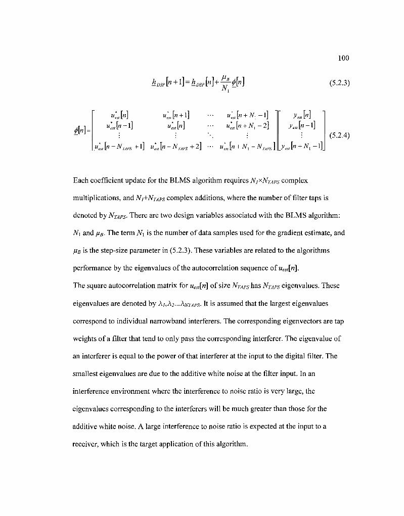
100
hDSp [«+1]=hosp M+-^-&n] (5.2.3)
M- <An + Nl-2]
U'eS, [" - NTAPS + !] * 4 [" - NTAPS + 2 ] • • • U'est [« + AT, - J V ^ ]_
(5.2.4)
Each coefficient update for the BLMS algorithm requires NJXNTAPS complex
multiplications, and NJ+NTAPS complex additions, where the number of filter taps is
denoted by NTAPS- There are two design variables associated with the BLMS algorithm:
N\ and JUB. The term N\ is the number of data samples used for the gradient estimate, and
fis is the step-size parameter in (5.2.3). These variables are related to the algorithms
performance by the eigenvalues of the autocorrelation sequence of uest[n].
The square autocorrelation matrix for uest[n] of size NTAPS has NTAPS eigenvalues. These
eigenvalues are denoted by XI,X2...XNTAPS. It is assumed that the largest eigenvalues
correspond to individual narrowband interferers. The corresponding eigenvectors are tap
weights of a filter that tend to only pass the corresponding interferer. The eigenvalue of
an interferer is equal to the power of that interferer at the input to the digital filter. The
smallest eigenvalues are due to the additive white noise at the filter input. In an
interference environment where the interference to noise ratio is very large, the
eigenvalues corresponding to the interferers will be much greater than those for the
additive white noise. A large interference to noise ratio is expected at the input to a
receiver, which is the target application of this algorithm.
101
Adaptive algorithms use feedback to adapt the filter taps. Feedback provides the potential
for an unstable system. The stability constraint for the standard BLMS algorithm is [44]:
2
Q < M B < — (5.2.5) max
Equation (5.2.5) shows the stability constraint is a function of the maximum eigenvalue
of the input signal's autocorrelation sequence. The maximum eigenvalue corresponds
approximately to the maximum interferer power in uest[ri]. A more conservative approach
involves replacing Xmax with the maximum power in ues,[n] [42]. This conservative upper
bound on //# removes any ambiguity associated with the assumption that the largest
interferer power is equal to Amax. The effect of errors in fe^M on stability is derived in
Section 5.3.1.
The mean-square error convergence time constant along the ktb eigenvector is [44]:
Nl Tk,MSE-l> 7~ (5.2.6)
LHBAk
Long convergence times are associated with small eigenvalues, which correspond to
weak interferers or white noise. Strong interferers have relatively large eigenvalues, so
the convergence at these frequencies will be faster. Fast convergence along the associated
eigenvectors requires a small N\ and large juB. A large interference to noise ratio results in
a large eigenvalue spread, which means that long convergence times will occur over the
smallest eigenvectors. The convergence rate along these eigenvectors is insignificant to
the interference attenuation of the total filter since they correspond to additive noise. The
convergence time also depends on the initialization of the filter coefficients [42].

102
The standard BLMS algorithm is modified for the hybrid RF-DSP FF filter. The
modification involves discarding Z23 values following a filter coefficient update. The
value of X23 is the effective length of the impulse response of fef"]- This modification
increases the convergence times, so the new convergence time constants are:
Nl Nl + L23 _ Nl + L23 T k,MSE — - , , r -> 1 (5.2.7)
2MB** NI 2 / " A
The numerator of (5.2.7) shows that the time constants cannot be significantly reduced
when Ni<L23, which is contrary to the standard BLMS.
The LMS algorithm estimates the gradient for each tap update. The accuracy of this
estimate depends on how many data samples are used for the estimate. Misadjustment is
the ratio of the mean square of the error signal of the adaptive filter in steady-state to that
of the Wiener filter. At steady-state, misadjustment is due to the noisy estimates of the
gradient. The misadjustment of the BLMS algorithm is [44]:
M=^tr(R) (5.2.8)
The trace operator (tr) of the input signal's correlation matrix (R) is the sum of the
eigenvalues. The largest eigenvalues dominate the misadjustment, as evident by (5.2.8).
The contribution to the misadjustment from the kth eigenvector with eigenvalue a*, is
liBOk I2N\. A small misadjustment requires a large N\ and a small fiB. These conditions
are in opposition to those for fast convergence; therefore demand a trade-off.
The adaptive algorithms are implemented in an FPGA for the hardware prototype;
therefore resource usage must factor into the trade-off. At every time instant a sample

103
from the error signal, yest[n\ is multiplied by a vector of current and past input signals,
{"«/[«], uest[n-l],.. .,uest[n-NTAPS*-l]} • This process requires NTAPS complex
multiplications every time sample. These products are accumulated for N\ samples
between updates. In terms of FPGA resources, there are NTAPS complex multiplications
every clock period, which is independent of M, therefore computational complexity is
not a factor in choosing N\.
In the literature pertinent to the BLMS algorithm [42,44], it is stated that if N\>NTAPS,
then redundant operations are performed as the digital filter cannot use all the input
information. These comments are directed at the BLMS in a different implementation, the
fast BLMS. In the fast BLMS the serialized input signals are converted to the frequency
domain before being processed by the NTAPS filter taps in the frequency domain. This
issue of redundant operations is not relevant to the implementation in this work as the
input signal is not transformed into the frequency domain. As Ni increases beyond NTAPS
the misadjustment continues to improve, but comes at the cost of an increased
convergence time.
The performance metrics that factor into the choice of N\ and juB are stability,
convergence rate, and misadjustment. These design variables are varied in the hardware
prototype, and the performance metrics are reported in Chapter 7.
5.2.3 Verification with Maximum Precision Simulation
The modified BLMS algorithm is implemented in Simulink. The digital filter has 64 taps
in the simulations (iVWs=64). The taps are initialized to 0. A 64 tap filter is also used to

104
represent fet"]- The algorithm used to obtain the 64 tap values of /i23,«f[n] is the topic of
the next section. Finite precision effects are deferred to Section 5.4.
The hybrid RF-DSP FF filter is simulated in the baseband domain. This approach avoids
the small time-steps required for RF signals. The block diagram used in Simulink is
shown in Fig. 5.2.8. The noise figures of the active analog components is set to 0 dB, and
the resolution of the digital components are set to maximum machine precision. These
settings isolate the results to measure the operation of the BLMS algorithm without
thermal or quantization noise effects. The time-step of the simulation is set to 2.5 nsec,
but the time-step of the digital components is set to 5 nsec. The larger time-step in the
digital components corresponds to a 200 MHz digital clock. The smaller step-size for the
analog components permits the T-BSF to have a relatively narrow notch.
Noise and c i Interference
C2 C3
coupl RF1
RF in Qg out
Mam Digital Filter RF2
In
Num
Digital 0 t
Filter Dig In RF out
T-BSF
thru Out
coupl
Terminate
coupl
RF3
RF in Dg out
Digital Filter
h23,est filter
AddgradEstto Downsample last Tap to discard data
LMS multiplication
grad Est new dig tap
lastTap
N1
-1 Z
Downsample by block size
Product
input signal gradEst
error signal
delay
Figure 5.2.8 - Simulink model of hybrid RF-DSP FF filter with h23,est[n\ known a
priori
The blocks in Fig. 5.2.8 that represent the hybrid RF-DSP FF filter in Fig. 5.2.1
excluding the algorithm processor are: CI, RFl, Main Digital Filter, RF2, T-BSF, C2, C3
and RF3. These blocks are the same as those from the noise analysis in the previous
chapter with the addition of RF3.
The remainder of the blocks in Fig. 5.2.8 form the algorithm processor, with the
exception of the Noise and Interference source. The h23,est filter block in Fig. 5.2.8
generates the uest[n\ samples, as shown in Fig. 5.2.6. These samples are processed by the
LMS multiplication block along with the yest[n\ samples from the RF3 block. This
processing is the matrix multiplication in (5.2.4). The vector product from this matrix
multiplication is the gradient estimate averaged over NTAPS values. In this simulation the
vector product is calculated every time step, but the BLMS algorithm only uses one of
these results every NTAPS time steps. The remainder NTAPS-1 values are discarded by the
first down-sample block. The second down-sample block is used to discard some of the
gradient estimates immediately after a tap update.
The Product and Add gradEst to last Tap blocks perform the filter tap update from
(5.2.3). The output of the latter block is the updated filter taps, which are then sent to the
main digital filter.
The Noise and Interference block in Fig. 5.2.8 generates an interference scenario. The
input PSD to the filter used in these simulations is shown in Fig. 5.2.9 with the 'PSDin'
curve. The input PSD represents multiple interferers, with various bandwidths and power
levels. This PSD is shown at baseband since the Simulink simulations are performed in
this domain.

106
-80
-100
n i r PSD.
PSD
i 1 r
Figure 5.2.9 - PSD at input and output of hybrid RF-DSP FF filter
The algorithm is run with M=64, and 64 data points discarded per update. The magnitude
response of the hybrid RF-DSP FF filter at two different time instants is shown in Fig.
5.2.10. These responses, denoted ti and t2, are recorded during the transient phase of the
filter's adaptation. The ti response occurs before t2. The solid dots on the -20 dB grid line
indicate the location of the interferers. Almost all of the dots have a notch going through
them. The exception is the wideband notch near -60 MHz, where a notch response forms
but does not reach -20 dB This figure demonstrates proper operation of the algorithm.
The magnitude responses at 20 and 62 MHz are zoomed in Fig. 5 2.11. These figures
show the improvement of the notch width as the filter adapts in time.

30
20
2. <u o at
a.-10
S-20 1-30 CO
5 - 4 0
-50
-61 00 -50
107
50 100 Frequency (MHz)
Figure 5.2.10 - Magnitude responses of hybrid RF-DSP FF filter during adaptation
15
^ 10
» i
k n kr <B V- -5 • o
5-10 c
| - 1 5
-20
-25
r - ^ t
/" \ / \
'. 12
1 ~\
W JO /"\ ^ WN ^ \ /
• —
/ ~x / / \ " '/ \ / \
V \ \ ' -
-19 20 21
Frequency (MHz) 58 60 62 64
Frequency (MMz) 66
Figure 5.2.11 - Zoomed responses from Fig. 5.2.10
Starting at time t2, the input and output samples are recorded and then processed to obtain
the PSD at the input and output of the hybrid RF-DSP FF filter. The results are shown in
Fig. 5.2.9. This response shows significant attenuation of the interferers at the expense of
an increase in the noise floor away from the receiver's passband (0 MHz).
The above results show successful operation of the FXBLMS with discard and hr>,es^n\
known a priori. Measurements of the hardware prototype are used to relate the
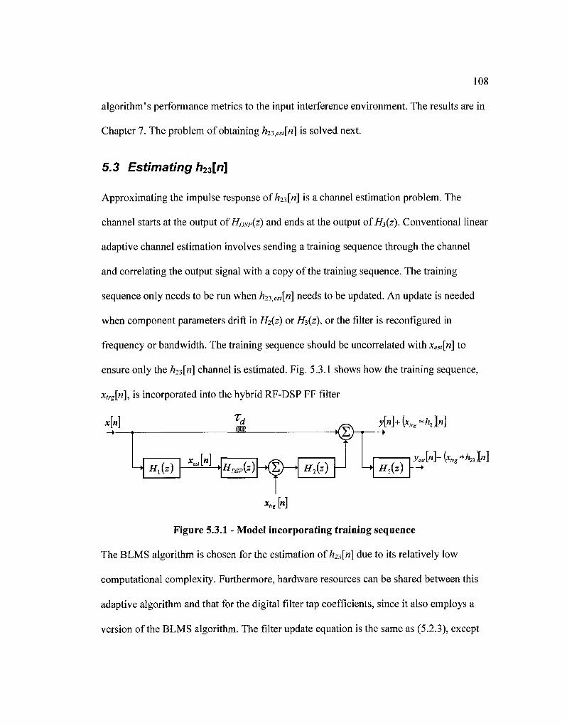
108
algorithm's performance metrics to the input interference environment. The results are in
Chapter 7. The problem of obtaining hn^st\ri\ is solved next.
5.3 Estimating h2z[n]
Approximating the impulse response of hn\ri\ is a channel estimation problem. The
channel starts at the output of HDsp(z) and ends at the output of Hi(z). Conventional linear
adaptive channel estimation involves sending a training sequence through the channel
and correlating the output signal with a copy of the training sequence. The training
sequence only needs to be run when h23,est[n] needs to be updated. An update is needed
when component parameters drift in H2(z) or H?,(z), or the filter is reconfigured in
frequency or bandwidth. The training sequence should be uncorrelated with xex([n] to
ensure only the h23[n] channel is estimated. Fig. 5.3.1 shows how the training sequence,
xtrg[n], is incorporated into the hybrid RF-DSP FF filter
c[n]
Hx{z) ,M HDSP{z) - < § ) - • H2{z)
- •
H3(z) ^M+tas*^ ! " ]
**g M
Figure 5.3.1 - Model incorporating training sequence
The BLMS algorithm is chosen for the estimation of h2?\n] due to its relatively low
computational complexity. Furthermore, hardware resources can be shared between this
adaptive algorithm and that for the digital filter tap coefficients, since it also employs a
version of the BLMS algorithm. The filter update equation is the same as (5.2.3), except
u[n] is replaced by xtrg[n], and yest[n] is replaced by yest[n]+(xtrg*h23)[n]. Discarding data
after filter updates is not required for this BLMS algorithm as the filter architecture does
not deviate from the conventional form.
The design variables relevant to this algorithm relate to the design of the training
sequence and the number of filter taps used in h2\est[n]. The training sequence will appear
as additive noise to the receiver. The PSD of the training sequence can be notched over
the receiver's passband to ensure negligible degradation to the receiver's sensitivity
performance. This training sequence characteristic is possible since an accurate estimate
of /?23[«] is not required in the passband since FF attenuation does not occur there.
Signals other than the training sequence appear as noise to the 23 [«] channel estimation
algorithm. These signals include the attenuated interferers in >><,,,[«], which do not have
flat PSD's, therefore cannot be treated as white noise. The frequency bands occupied by
these interferers correspond to the frequencies where the most accurate estimate of //23 [«]
is required. Errors in the estimate of h23[n] affect the performance metrics of the main
digital filter's LMS algorithm, including stability. These effects are derived next.
5.3.1 Effect of Errors in Ai23,est[n]
Since /?23,e [«] does not exactly equal feM, then uest[n] will not exactly equal u[n]. The
performance metrics of the LMS algorithm are based on the input signal u[n] and not
uest[ri\, but the latter is used by the FXBLMS with discard algorithm.
One effect of magnitude mismatch in /j23,ew[w] is to cause pre-emphasis or de-emphasis of
incoming interference signals. For example, if fe^M is 3 dB larger than hn\ri\ over a
frequency band occupied by an interferer, then the FXBLMS algorithm will treat the

110
interferer like it is 3 dB larger and attenuate it more than is required to produce a white
noise output. These effects shift the convergence point in the goal function of the LMS
algorithm. In an RF environment with a large interference to noise ratio, the convergence
point shift is negligible when the magnitude error is only a few decibels at interferer
frequencies. The magnitude error can be even larger at frequencies occupied only by
noise.
A more degrading effect of mismatch between /?23,e [«] and h23[n] is to bias the gradient
estimate during adaptation. The following analysis switches from a block to a sample
based adaptive algorithm. This switch does not impact the solution, but allows for more
concise mathematical expressions. The expected value of the estimated gradient for this
modified LMS algorithm is:
The estimate of the input signal can be decomposed into the desired term and an error
term:
"«,["] = «["]+«.ir W (5-3.2)
Similarly, the estimate of the impulse response of feM can be decomposed:
^ M ^ B M + ^ M (5-3.3)
The estimate in (5.3) is expanded with (5.3.2):
E[VjJ = E[uin)y:Xn)}+E[uJn)y;sl(n)} (5-3-4)
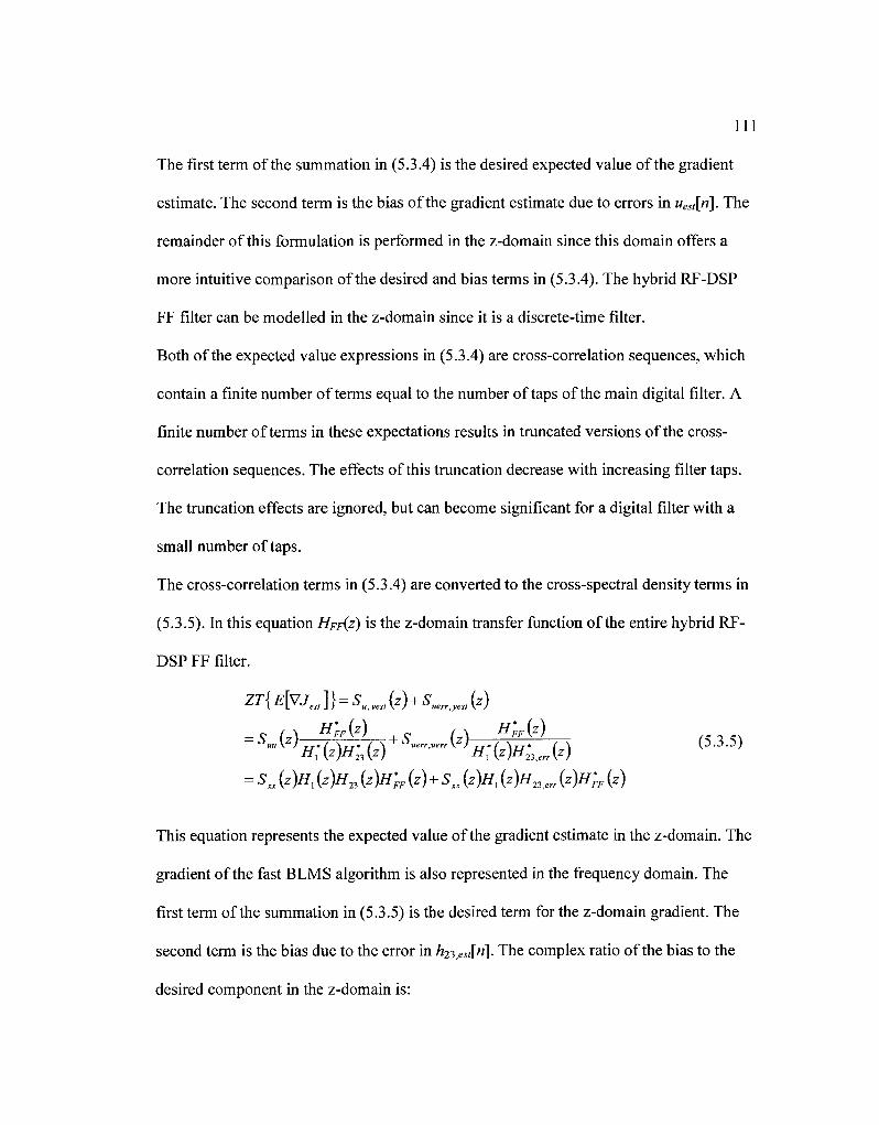
I l l
The first term of the summation in (5.3.4) is the desired expected value of the gradient
estimate. The second term is the bias of the gradient estimate due to errors in ues,[n]. The
remainder of this formulation is performed in the z-domain since this domain offers a
more intuitive comparison of the desired and bias terms in (5.3.4). The hybrid RF-DSP
FF filter can be modelled in the z-domain since it is a discrete-time filter.
Both of the expected value expressions in (5.3.4) are cross-correlation sequences, which
contain a finite number of terms equal to the number of taps of the main digital filter. A
finite number of terms in these expectations results in truncated versions of the cross-
correlation sequences. The effects of this truncation decrease with increasing filter taps.
The truncation effects are ignored, but can become significant for a digital filter with a
small number of taps.
The cross-correlation terms in (5.3.4) are converted to the cross-spectral density terms in
(5.3.5). In this equation HFF{Z) is the z-domain transfer function of the entire hybrid RF-
DSP FF filter.
ZT{ E[vjesl ]} = Su,yest (z) + Suerryesl (z)
- c (A H'FFJZ) , o (A H'FF(Z) ~ , «
Hx {z)H23 (z) H, [z)Hnerr [z)
= Sxx {z)H, (z)//23 (z)H;F (Z)+SXX {Z)H{ {z)H23err (z)H'FF (Z)
This equation represents the expected value of the gradient estimate in the z-domain. The
gradient of the fast BLMS algorithm is also represented in the frequency domain. The
first term of the summation in (5.3.5) is the desired term for the z-domain gradient. The
second term is the bias due to the error in h23,est[n]. The complex ratio of the bias to the
desired component in the z-domain is:

112
_ - " 23,err \Z) . . _ , . Ygrad — TT ( \ (j.i.O)
H23[z)
The ratio in (5.3.6) is defined to permit the expected value of the gradient estimate in the
z-domain to be expressed as:
ZT{E[VJes, ]} = ZT{E[Vj]}x (l + ygmd ) (5.3.7)
The weight update equation of the adaptive algorithm is written in the z-domain with the
estimated gradient substituted for the actual gradient:
HDSP{k + l)=HDSP(k)-^-xZT{E[w]}x{l + rgrad) (5.3.8)
The HDSp terms are the main filter's tap values in the z-domain. The step-size parameter
of the weight update in (5.3.8) is effectively changed to:
MB,eff=MB(l + rgrad) (5.3.9)
This effective step-size parameter is frequency dependent due to the frequency dependent
behaviour of ygrad, defined in (5.3.6). If the value of ftB.effis different than fiB at
frequencies occupied by interferers, then the stability, convergence time and
misadjustment along the corresponding eigenvectors are different than if the step-size
was just fiB- The standard LMS algorithm uses real values for the step-size parameter, but
here the effective value is complex, which requires re-working of the performance
metrics in (5.2.5), (5.2.7) and (5.2.8).
Complex issues related to adaptive filters are typically illustrated with a two tap filter
example such that the goal function can be plotted in 2-D. The adaptation of a two tap
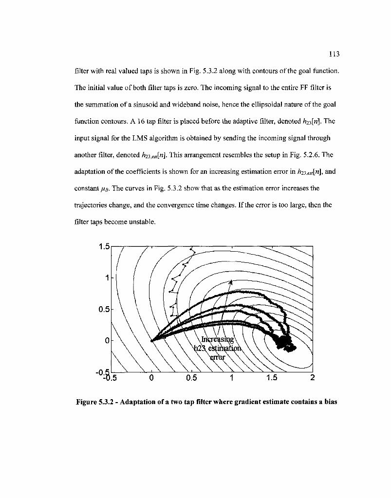
113
filter with real valued taps is shown in Fig. 5.3.2 along with contours of the goal function.
The initial value of both filter taps is zero. The incoming signal to the entire FF filter is
the summation of a sinusoid and wideband noise, hence the ellipsoidal nature of the goal
function contours. A 16 tap filter is placed before the adaptive filter, denoted hn\n\. The
input signal for the LMS algorithm is obtained by sending the incoming signal through
another filter, denoted /i23,est[ri\. This arrangement resembles the setup in Fig. 5.2.6. The
adaptation of the coefficients is shown for an increasing estimation error in h23,est[n], and
constant HB. The curves in Fig. 5.3.2 show that as the estimation error increases the
trajectories change, and the convergence time changes. If the error is too large, then the
filter taps become unstable.
Figure 5.3.2 - Adaptation of a two tap filter where gradient estimate contains a bias

114
The remainder of this section is dedicated to relating the stability constraint of the main
filter's adaptive algorithm and errors in Hn,est{z)- A more general version of the LMS
small step-size stability constraint is [42]:
|1- /V*, |<1 (5-3.10)
To determine the effect of ygrad on stability, the effective step-size from (5.3.9) is
substituted into this LMS stability constraint:
- ! - - 1
In the complex plane (5.3.11) defines a circle with radius V/ish offset from the origin by
a distance of 1/^BK - 1 along the real axis. The value of this offset term can be positive
or negative. The area enclosed by each circle represents a feasibility region for ygrad to
ensure stability. Several feasibility circles are plotted in Fig. 5.3.3, each for a different
value of the original step-size, [iB-
MB*, (5.3.11)

115
-1 0 1 R e a l<W
Figure 5.3.3 - Feasibility region of ygrad for various values of juB
In the above figure the magnitude of ygrad is the radial distance from the origin, and the
phase of ygrad is the angle from the positive real axis. Each circle in Fig. 5.3.3 encloses a
region where the FXBLMS with discard algorithm will be stable, for the specified /uB,
along the eigenvector corresponding to X. The region constrains the values of ygraij to
ensure stability.
The feasibility circles in Fig. 5.3.3 become larger as the value of pB decreases, which
permits larger estimation errors in /?23,e [«]. In this biased LMS algorithm, the
convergence time is still inversely proportional to fig, so decreasing fiB to an arbitrarily
small value is not the optimal approach. Furthermore, regardless of how large the
feasibility circle is, there is only a small feasibility region when the angle of ygrad is
greater than n/2 and less than 37t/2. Permitting large errors in /z23,e«[«] may land the angle
of ygrad in this range within the band of an interferer and cause the algorithm to become
unstable.
Each eigenvector has its own feasibility region for ygrad, for a fixed value of //g. In a
relatively narrowband interference environment with a large interference to noise ratio,
each eigenvector is fairly restricted to a frequency band occupied by an interferer. The
associated eigenvalue is the interferer power, and ygrad is a measure of the estimation
error in fe.^M within that band. Eigenvectors with large eigenvalues correspond to
small circles within Fig. 5.3.3, therefore at these frequencies the estimation error in
h23,est[n] must be relatively small. Eigenvectors corresponding to wideband noise have
small eigenvalues, which have very large feasibility circles in Fig. 5.3.3. The estimation
error in h23^st[ri\ is less critical at frequency bands not occupied by interferers.
The results in this section are important because they determine how accurately the
h23,est[n] filter must model the h23[n] channel. The filter's design parameters that affect
this accuracy are the number of filter taps, number of samples per update, and the step-
size parameter of the /Z23M channel estimation algorithm.
5.4 Algorithm for Tunable BSF Control
The tunable BSF is adaptive for two reasons. First, the components within the BSF may
drift, thereby degrading the depth of the transfer function notch. Second, the frequency
agility characteristic of the hybrid RF-DSP FF filter requires the T-BSF's notch to be
frequency agile. The BSF used in the hardware prototype consists of two paths in FF,
with one path containing a vector modulator and the other a delay line. The block
diagram in Fig. 5.4.1 shows this BSF configuration within the hybrid RF-DSP FF filter.

117
«M JUL
HXA x,An]
HDSP{z) H2{. •K VM (•»
T Y -/
-*y\ [n]
ZMlZM C^RFl.ADC's DAC's,
RF2,C2
BSF C3, RF7>, ADC's
Figure 5.4.1 - BSF algorithm implementation
The notch is required in the receiver's passband, but signals in this band are not easily
detected in the presence of strong interferers. The purpose of a BTS receiver is to receive
signals in this passband, so the digital output of this receiver can be used as a feedback
signal to adapt the notch. This feedback path would have significant latency, but drifting
of the BSF components is very slow; therefore can be afforded.
A second method was used to tune the BSF without requiring a BTS receiver. This
method has the FPGA inject a double sideband tone into the receiver's passband during
adaptation of the BSF. The two vector modulator baseband inputs are varied over their
entire ranges and the power of the tone is recorded at the output of the ADC's in the
feedback path. The vector modulator inputs that result in the minimum power at these
ADC's are locked in and the tone turned off. This algorithm only needs to run when the
frequency is changed, or the BSF notch components significantly drift. Successful tuning
of the BSF is demonstrated in the following chapter.
5.5 Finite Precision Effects
The simulation results in the previous sections used maximum floating point precision in
Simulink. Finite precision effects were incorporated into the noise analysis in Chapter 4.
Another effect of finite precision is to bias the tap weights of an adaptive filter. This bias

118
is most problematic for adaptive filters that adapt over a long period of time [42].
Furthermore, finite precision limits the maximum tap values.
Finite precision is incorporated into the Simulink simulations by using the fixed-point
toolbox. The tap coefficients for h23,est[ri] are known a priori. The evolution of the 32
complex taps of the main digital filter is shown in Fig. 5.5.1. The bias due to finite
precision is apparent in these figures by the slowly increasing curves from between
iterations 1 and 6xl05. These signed taps are represented with 15 bits, which can take on
a maximum value of 214-1 (shown in each of the figures as a thick horizontal line). The
bias due to finite precision results in a consistent increase of some of the tap values.
Eventually one of these taps hits the saturation level, and the filter performance becomes
unpredictable. The coefficients appear to somewhat settle after iteration 6x 10⁵, but the
bias again pushes them towards the saturation level just before iteration 12x 105.
Fortunately this bias problem is well known and the solution is to modify the LMS
algorithm by using the leaky LMS algorithm [42].
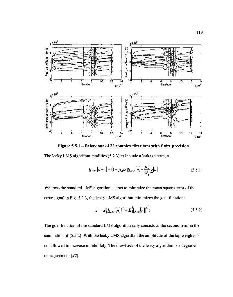
119
2
2 1 V) Q.
5° (0
ctt
-•3
x104
J. i l l
i .
r
M ^ 1 " ,r^rlfr •Atz/t^ir^"" i
1 •
i k
„x10
CO
?1
S 0 •5
a v 0£
6 8 Iteration
10 12 x10
-2,
r '/^srzrt
fc^^^
6 8 Iteration
10 12 x10
,x10 x10
x10
6 8 Iteration
10 12 x10
Figure 5.5.1 - Behaviour of 32 complex filter taps with finite precision
The leaky LMS algorithm modifies (5.2.3) to include a leakage term, a.
how [" +1] = (l - MB^DSP M + ^-£["1 (5.5.1)
Whereas the standard LMS algorithm adapts to minimize the mean square error of the
error signal in Fig. 5.2.3, the leaky LMS algorithm minimizes the goal function:
The goal function of the standard LMS algorithm only consists of the second term in the
summation of (5.5.2). With the leaky LMS algorithm the amplitude of the tap weights is
not allowed to increase indefinitely. The drawback of the leaky algorithm is a degraded
misadjustment [42].
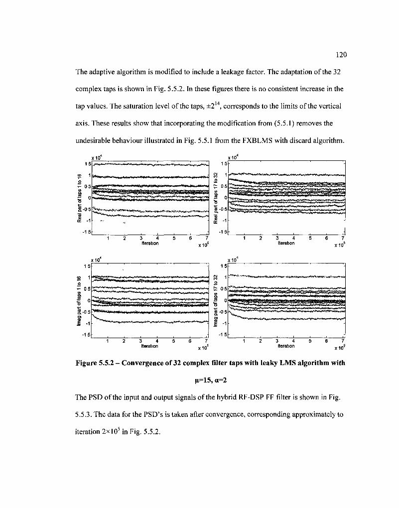
120
The adaptive algorithm is modified to include a leakage factor. The adaptation of the 32
complex taps is shown in Fig. 5.5.2. In these figures there is no consistent increase in the
tap values. The saturation level of the taps, ±214, corresponds to the limits of the vertical
axis. These results show that incorporating the modification from (5.5.1) removes the
undesirable behaviour illustrated in Fig. 5.5.1 from the FXBLMS with discard algorithm.
x10 x10 15
1
; jTytiTTTii" " "f"ft'iii*n n^n**-i**rLiii'ftiiirt'ir»»iju(i>.
rf^v^v***<»<i*i,^Art0m\)i'*"#*1fi*,***w*mm* w y w«l*t'>»«»w*w>t#NN>*<'<U|Mi
*- 0 5*3GEI 0
0
-0
-1
-15
f* 'aWMrflNft i •» iWwWftyyw ^atfft»*NMIMMi' • \m >W Wwflhfc*'!
15
i****1'—tw***^''*vrJ'f''*—*"**i ^—f^irwrt-iiintrv. * jiH " !1f.ji-ifcrtV«¥ii i r w » » ^
o £ 05 u> Q. S 0
•s
-15-2 3 4
Iteration x10
3 4 Iteration x10
x10 x10 1 5
1
05
0
-0 5
-1
-1 5
~»-^MI.II..1I>IJW^»MI ••'«i'HUu>wDnM«ii»iiiMijj»JiB«iaiii mf*> ^CMIIiUJHM^ *i|i>i>ii'»<lii l |i»i li.*;;Wi..T|ii».,i i> nni;»niiiriinM.ii'
1 5
05 ••hftBI*!**.
-1 5 -
M, '«' 'Wfl(H**M4»-W<fc*»i«^*^^
l f c *%nr^ i^Mf > i i ^^ w . ^n i« )W^ i^ i^^» iY^ | i - ^M^-Mr , y* r ' ' ^ 1 i r ' I " *>" I * r^''i«* ' V n i 1 J
3 4 Iteration x10
3 4 Iteration x10
Figure 5.5.2 - Convergence of 32 complex filter taps with leaky LMS algorithm with
u=15, a=2
The PSD of the input and output signals of the hybrid RF-DSP FF filter is shown in Fig.
5.5.3. The data for the PSD's is taken after convergence, corresponding approximately to
iteration 2xl05 in Fig. 5.5.2.

121
-60
-80
_-100 N I *g-120 m a-140 w
°--160
-180
"2-5oO -100 0 100 200
Frequency (MHz)
Figure 5.5.3 - PSD of input and output signals of hybrid RF-DSP FF filter
Narrowband and wideband attenuation of multiple interferers can be seen in Fig. 5.5.3,
with finite precision incorporated into the simulations. The performance of the algorithms
is deferred to the following chapters since the hardware prototype offers a much faster
means of processing the data.
5.6 Algorithm Development Summary
This chapter has introduced the algorithms for the hybrid RF-DSP FF filter. Adaptive
algorithms are required to handle a dynamic interference environment and drift of the RF
and analog components. The algorithm that adapts the main digital filter is based on a
block implementation of the FXLMS algorithm. Data discard is incorporated into this
algorithm so the performance metrics from the standard block LMS algorithm can be
used; namely stability, convergence time and misadjustment. A leakage factor is
incorporated to compensate for finite precision effects. This algorithm requires
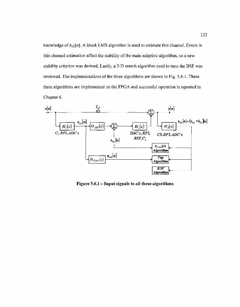
122
knowledge of feM- A block LMS algorithm is used to estimate this channel. Errors in
this channel estimation affect the stability of the main adaptive algorithm, so a new
stability criterion was derived. Lastly, a 2-D search algorithm used to tune the BSF was
reviewed. The implementations of the three algorithms are shown in Fig. 5.6.1. These
three algorithms are implemented on the FPGA and successful operation is reported in
Chapter 6.
«M rM
H{{z) M
Cl7RFl,ADC's
HDSP(Z) K2{z) Hjz) J>««[»]+(*»***B)["]
DAC's,RF2, C3,RF3,ADC\
>] BSF,C2
H23,est(z) ««.[«]
Algorithm
Tap Algorithm
BSF Algorithm
Figure 5.6.1 - Input signals to all three algorithms
6 Hardware Prototype
The analyses and simulation results in the two previous chapters showcase the potential
for the hybrid RF-DSP FF filter in the RF front-end of a BTS receiver. This chapter
describes the hardware prototype and demonstrates proper operation of the algorithms.
The next chapter reports the performance of the hardware prototype for various input
interference scenarios and filter realizations.
6.1 Description of Components
The hardware prototype consists of evaluation boards and discrete connectorized
components. A block diagram of the hardware prototype is shown in Fig. 6.1.1, and a
photograph in Fig. 6.1.2. Torque wrenches are standing in the photograph at the RF input
and output of the hybrid RF-DSP FF filter. The evaluation boards are summarized in
Table 6.1, and the connectorized components in Table 6.2. In the figure and tables the
prefixes C, G and D denote couplers, amplifiers, and delay lines, respectively. The vector
modulator within the BSF is denoted by VMOD, and the 3-dB splitter by SPLIT.
The LPF's adjacent to the primary ADC's and DAC's are not present in the hardware
prototype since they significantly increase the group delay of the lower FF path. The
additional group delay is shown in Section 6.2.7.
123
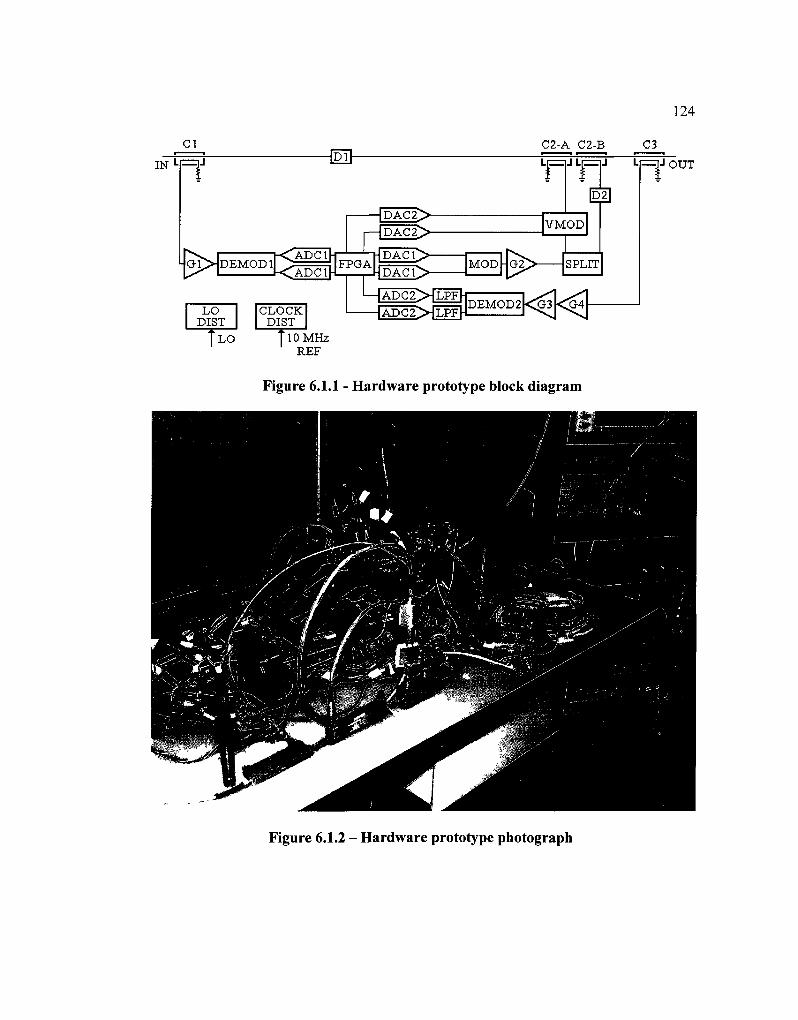
124
ci
IN = | J n C2-A C2-B
•nJH |D2
-G£> DEM0D1 < A D C l h
LO DIST
fTo
< A D C l r
-[DAC2>-
> pfDAC2>
H|DAC1>"
VMOD
CLOCK DIST
TTo
FPGA I ^
rJ{DACT> I—{ADC2>{LPF|-
MOD - G 2 > SPLIT
HADC2>JLPFT- DEMOD2 G3KG4
MHz REF
C3
n J OUT
Figure 6.1.1 - Hardware prototype block diagram
Figure 6.1.2 - Hardware prototype photograph
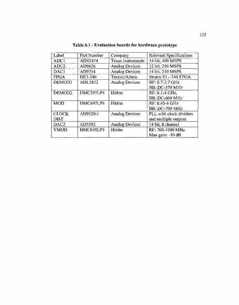
Table 6.1 - Evaluation boards for hardware prototype
Label ADC1 ADC2 DAC1 FPGA DEMOD1
DEMOD2
MOD
CLOCK DIST DAC2 VMOD
Part Number ADS5474 AD9626 AD9744 DE3-340 ADL5832
HMC597LP4
HMC697LP4
AD9520-1
AD5392 HMC630LP3
Company Texas Instruments Analog Devices Analog Devices Terasic/Altera Analog Devices
Hittite
Hittite
Analog Devices
Analog Devices Hittite
Relevant Specifications 14 bit, 400 MSPS 12 bit, 250 MSPS 14 bit, 210 MSPS Stratix III - 340 FPGA RF: 0.7-2.7 GHz BB: DC-370 MHz RF: 0.1-4 GHz, BB: DC-600 MHz RF: 0.45-4 GHz BB: DC-700 MHz PLL with clock dividers and multiple outputs 14 bit, 8 channel RF: 700-1000 MHz Max gain: -10 dB
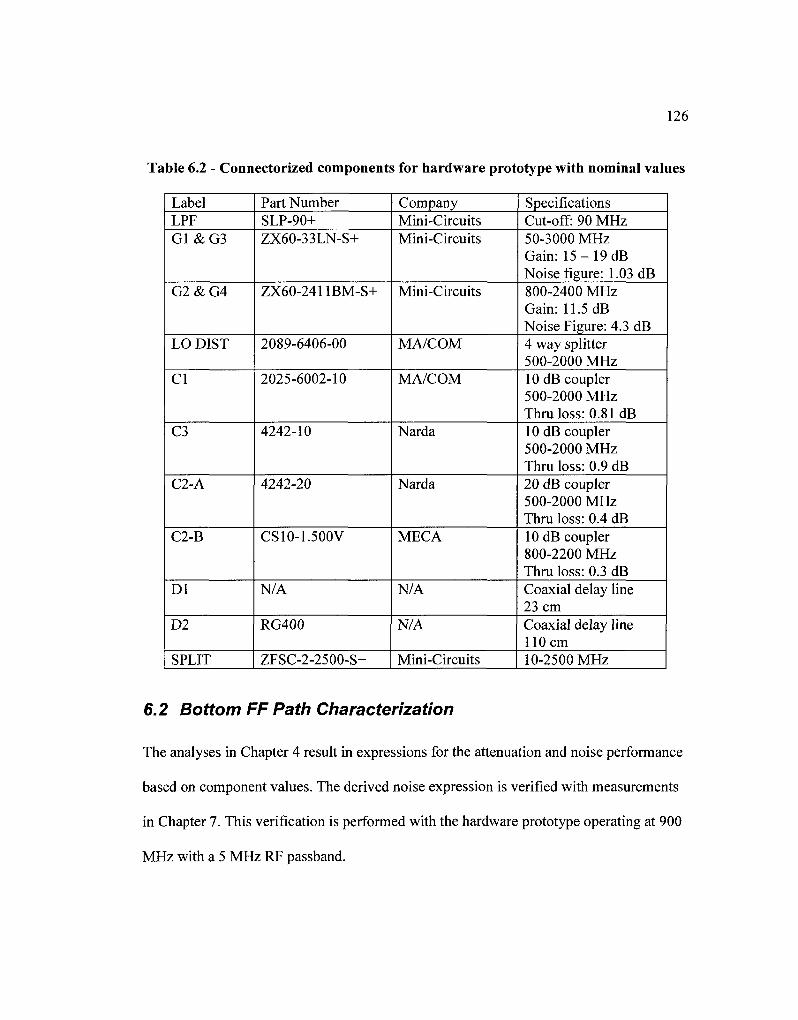
126
Table 6.2 - Connectorized components for hardware prototype with nominal values
Label LPF G1&G3
G2&G4
LO DIST
CI
C3
C2-A
C2-B
Dl
D2
SPLIT
Part Number SLP-90+ ZX60-33LN-S+
ZX60-2411BM-S+
2089-6406-00
2025-6002-10
4242-10
4242-20
CS10-1.500V
N/A
RG400
ZFSC-2-2500-S+
Company Mini-Circuits Mini-Circuits
Mini-Circuits
MA/COM
MA/COM
Narda
Narda
MECA
N/A
N/A
Mini-Circuits
Specifications Cut-off: 90 MHz 50-3000 MHz Gain: 1 5 - 1 9 d B Noise figure: 1.03 dB 800-2400 MHz Gain: 11.5 dB Noise Figure: 4.3 dB 4 way splitter 500-2000 MHz 10 dB coupler 500-2000 MHz Thru loss: 0.81 dB 10 dB coupler 500-2000 MHz Thru loss: 0.9 dB 20 dB coupler 500-2000 MHz Thru loss: 0.4 dB 10 dB coupler 800-2200 MHz Thru loss: 0.3 dB Coaxial delay line 23 cm Coaxial delay line 110 cm 10-2500 MHz
6.2 Bottom FF Path Characterization
The analyses in Chapter 4 result in expressions for the attenuation and noise performance
based on component values. The derived noise expression is verified with measurements
in Chapter 7. This verification is performed with the hardware prototype operating at 900
MHz with a 5 MHz RF passband.
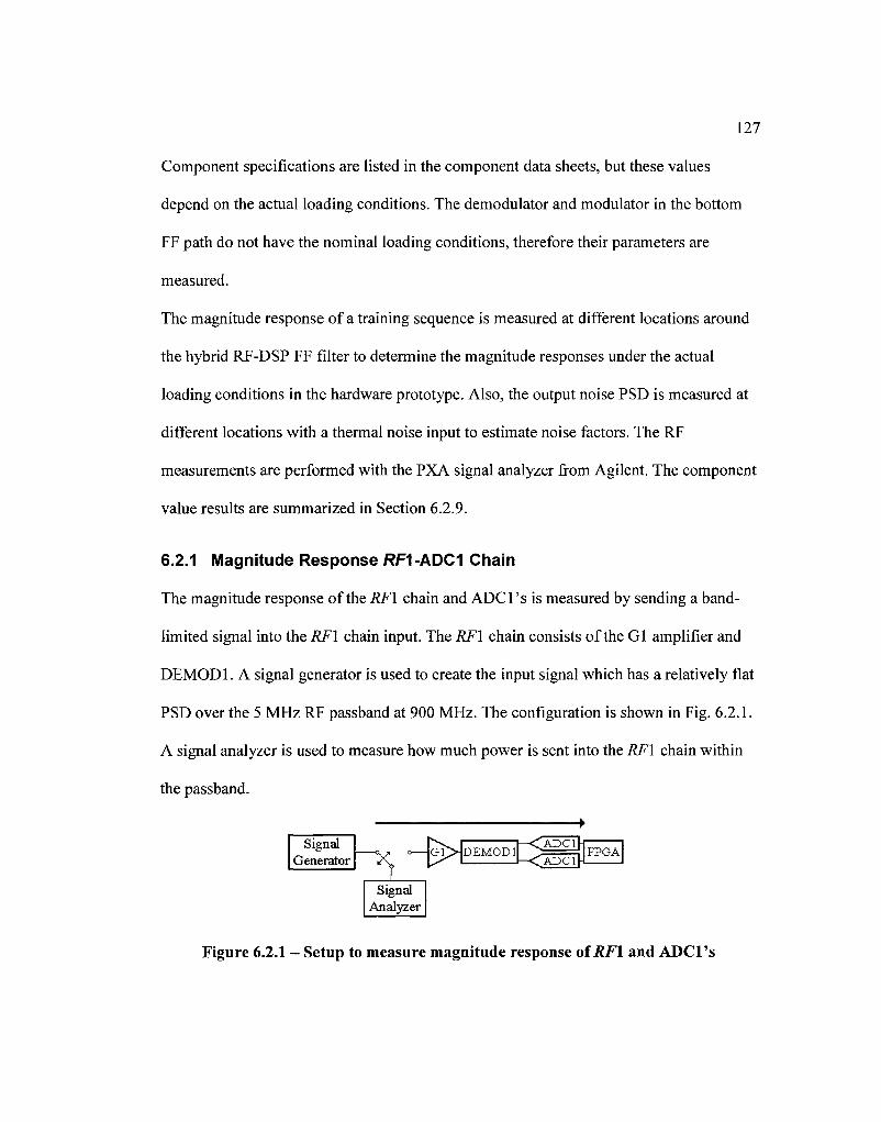
127
Component specifications are listed in the component data sheets, but these values
depend on the actual loading conditions. The demodulator and modulator in the bottom
FF path do not have the nominal loading conditions, therefore their parameters are
measured.
The magnitude response of a training sequence is measured at different locations around
the hybrid RF-DSP FF filter to determine the magnitude responses under the actual
loading conditions in the hardware prototype. Also, the output noise PSD is measured at
different locations with a thermal noise input to estimate noise factors. The RF
measurements are performed with the PXA signal analyzer from Agilent. The component
value results are summarized in Section 6.2.9.
6.2.1 Magnitude Response RF1-ADC1 Chain
The magnitude response of the RFl chain and ADC1 's is measured by sending a band-
limited signal into the RFl chain input. The RFl chain consists of the Gl amplifier and
DEMODl. A signal generator is used to create the input signal which has a relatively flat
PSD over the 5 MHz RF passband at 900 MHz. The configuration is shown in Fig. 6.2.1.
A signal analyzer is used to measure how much power is sent into the RFl chain within
the passband.
•
Signal Generator N DEMODl
ADC1 J—<ADC1|
FPGA
Signal Analyzer
Figure 6.2.1 - Setup to measure magnitude response of RFl and ADCl's
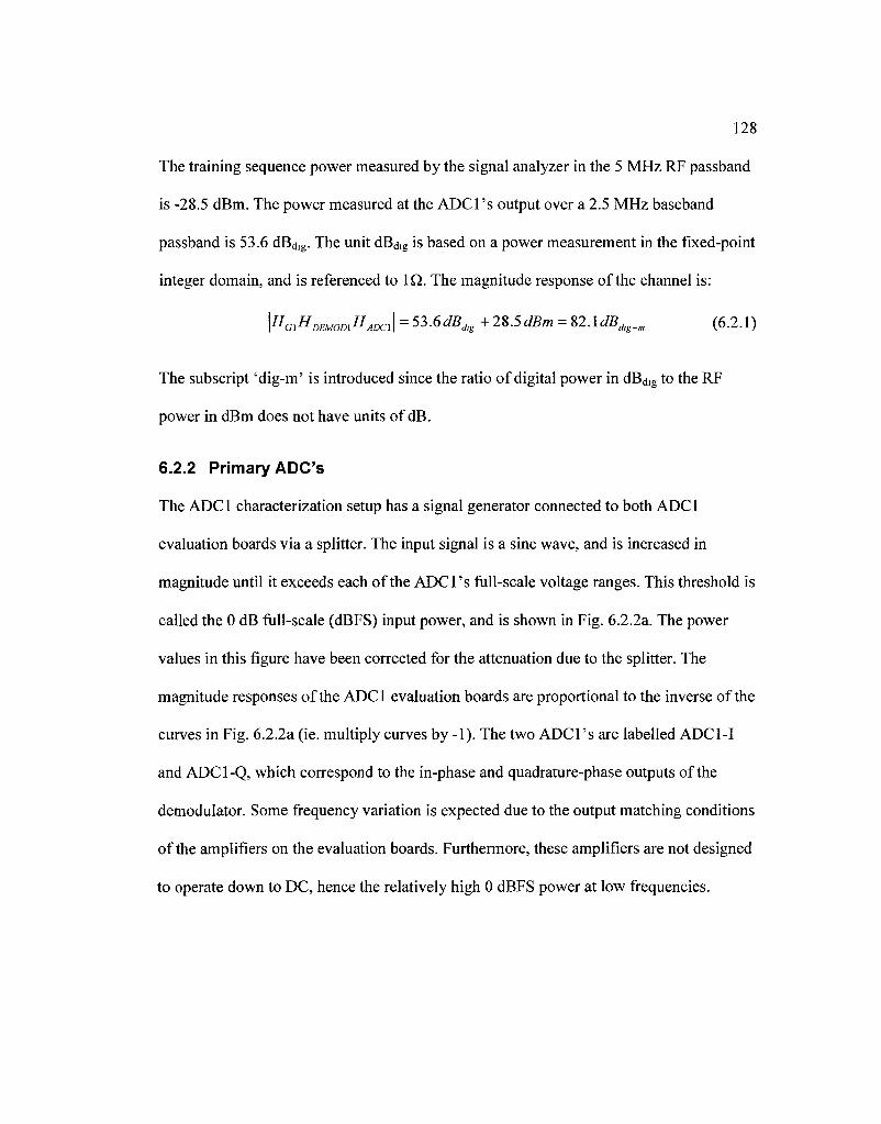
128
The training sequence power measured by the signal analyzer in the 5 MHz RF passband
is -28.5 dBm. The power measured at the ADCl's output over a 2.5 MHz baseband
passband is 53.6 dBdlg. The unit dBd,g is based on a power measurement in the fixed-point
integer domain, and is referenced to 1Q. The magnitude response of the channel is:
\HGlHDEMOmHADCl\ = 53.6dBdlg + 2S.5dBm = S2.ldBdlg_m (6.2.1)
The subscript 'dig-m' is introduced since the ratio of digital power in dBdlg to the RF
power in dBm does not have units of dB.
6.2.2 Primary ADC's
The ADCl characterization setup has a signal generator connected to both ADCl
evaluation boards via a splitter. The input signal is a sine wave, and is increased in
magnitude until it exceeds each of the ADCl's full-scale voltage ranges. This threshold is
called the 0 dB full-scale (dBFS) input power, and is shown in Fig. 6.2.2a. The power
values in this figure have been corrected for the attenuation due to the splitter. The
magnitude responses of the ADCl evaluation boards are proportional to the inverse of the
curves in Fig. 6.2.2a (ie. multiply curves by -1). The two ADCl's are labelled ADC1-I
and ADC1-Q, which correspond to the in-phase and quadrature-phase outputs of the
demodulator. Some frequency variation is expected due to the output matching conditions
of the amplifiers on the evaluation boards. Furthermore, these amplifiers are not designed
to operate down to DC, hence the relatively high 0 dBFS power at low frequencies.
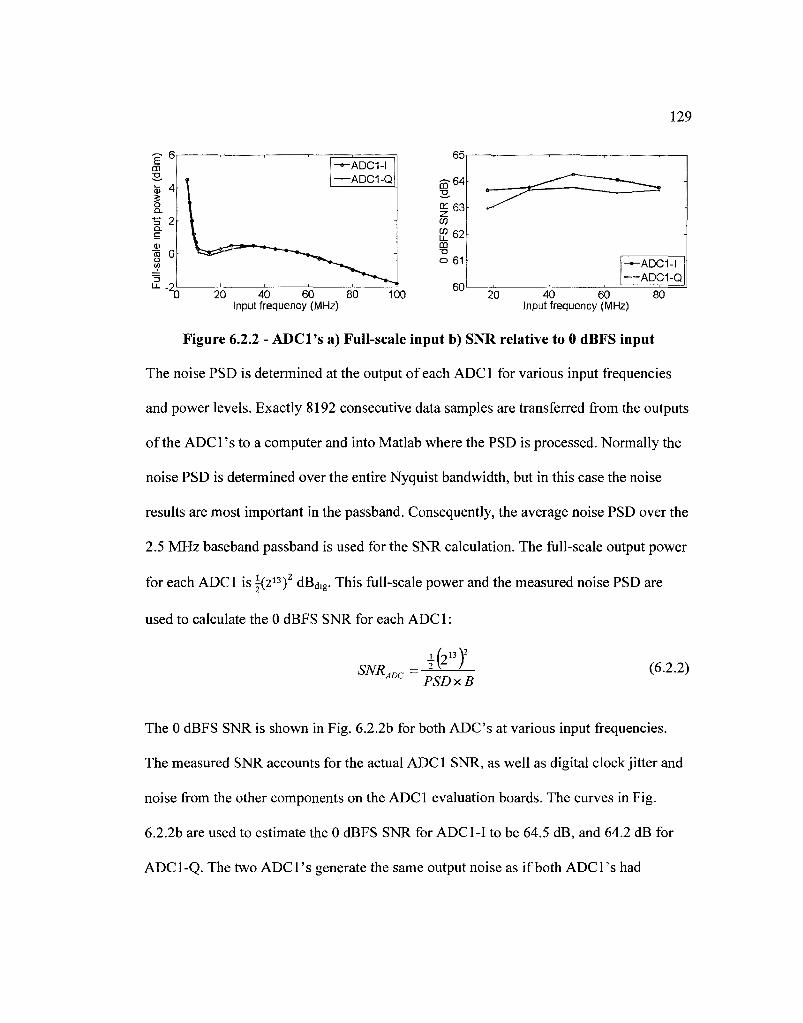
129
-•-ADC1-I —ADC1-Q
65
m 6 4
33,
I 63 CO
CD
o 61
20 40 60 80 Input frequency (MHz)
60 > < 1
-
-—ADC1-I i
—ADC1-Q
20 40 60 80 Input frequency (MHz)
Figure 6.2.2 - ADCl's a) Full-scale input b) SNR relative to 0 dBFS input
The noise PSD is determined at the output of each ADC1 for various input frequencies
and power levels. Exactly 8192 consecutive data samples are transferred from the outputs
of the ADCl's to a computer and into Matlab where the PSD is processed. Normally the
noise PSD is determined over the entire Nyquist bandwidth, but in this case the noise
results are most important in the passband. Consequently, the average noise PSD over the
2.5 MHz baseband passband is used for the SNR calculation. The full-scale output power
for each ADC1 is j(213)2 dBdlg. This full-scale power and the measured noise PSD are
used to calculate the 0 dBFS SNR for each ADC1:
SNR ADC PSDxB (6.2.2)
The 0 dBFS SNR is shown in Fig. 6.2.2b for both ADC's at various input frequencies.
The measured SNR accounts for the actual ADC1 SNR, as well as digital clock jitter and
noise from the other components on the ADC1 evaluation boards. The curves in Fig.
6.2.2b are used to estimate the 0 dBFS SNR for ADC1-I to be 64.5 dB, and 64.2 dB for
ADC1-Q. The two ADC1 's generate the same output noise as if both ADC1 's had

130
identical SNR's of 64.3 dB. This SNR is used in place of SNRADC for the output noise
expression.
6.2.3 Noise Factor of RF1 Chain
The noise factor of the RFl chain is obtained by measuring the output noise of the
ADC1 's when the input PSD to the RFl chain is kT0 over the 5 MHz RF passband. A
sine wave is also injected into the RFl input to ensure the inputs to the data converters
span several quantization levels. A directional coupler is used to inject the sine wave as
shown in Fig. 6.2.3.
•
C 1 | \ . I 1—<ADClhf DEMODl
—<ADClh FPGA
Signal Generator
Figure 6.2.3 - Setup to measure noise factor of RFl
The PSD in the passband of the complex digital output signal from the ADC1 's is:
IrT 4-lrT —OlrTF Iff H H I2 p 2 I ^DC,fs\ (6 2 3) K*ADc-i + K1 ADC-Q ~ ^K1 §rjtf\\riGxnDEUOmnADCX\ + Z X V • • )
*NKADCB
The output noise PSD for each ADC1 is expressed in terms of its equivalent noise
temperature in (6.2.3). The digital PSD on the left side of (6.2.3) is measured for different
input signal levels and frequencies from the signal generator. On average this value in the
passband is -61.0 dBdig/Hz, The noise factor of the RFl chain in (6.2.3) is solved using:
• 5=100 MHz, vADCfs=±2u (since ADC has 14 bits)
• SNRADC = 64.3 dB (from Section 6.2.2)

131
• \HG\HDEMOD\HADC\ 1=82.1 dBdlg-m (from Section 6.2.1)
The result of these substitutions is a noise figure estimate of: FRFI=26.2 dB.
The noise figure of the RFl chain is next used to isolate the noise factor of the DEMODl
component.
F — F I DEMODl ~ 1 _ ^ 77 _ f z 7 _ 17 \ t r I2 , 1 . , „ . . rRFl rGl~r I i2 ^DEMODl ~ V RFl rGlJ\ Gl\ (6.2.4)
Poil
The gain and noise factor of the Gl amplifier are 19.2 dB and 1.03 dB, respectively.
Substituting these values and FRF\ into (6.2.4) yields: FDEMOD\= 45.3 dB. Furthermore,
substituting the gain of Gl into (6) gives: \HDEMOD\HADCI\=62.9 dBd,g-m- These magnitude
terms do not need to be separated for the output noise expression, so the 62.9 dB is
arbitrarily distributed as: \HDEMOD\\=2.9 dB, and \HADC\\=6Q dBdlg.m. The full-scale digital
value of the ADCl's in this test is ±213, so according to (4.1.7) the average 0 dBFS input
power of the ADCl's over the passband is: PADC,FS=15-3 dBm.
6.2.4 Magnitude Response DAC-RF2 Chain
A training sequence with a uniform PSD is generated in the FPGA and sent through the
DAC's, then measured by a signal analyzer at the output of the lower FF path. The RFl
chain consists of the MOD and G2 amplifier. This setup is demonstrated in Fig. 6.2.4.
FPGA DAC1
DAC1 MODHG2, Signal
Analyzer
Figure 6.2.4 - Setup to measure magnitude response of the DAC's and RFl
The training sequence power in the digital domain has 70.5 dBdig of power over the
Nyquist bandwidth; which has 54.5 dBdlg of power in a 2.5 MHz baseband passband. The
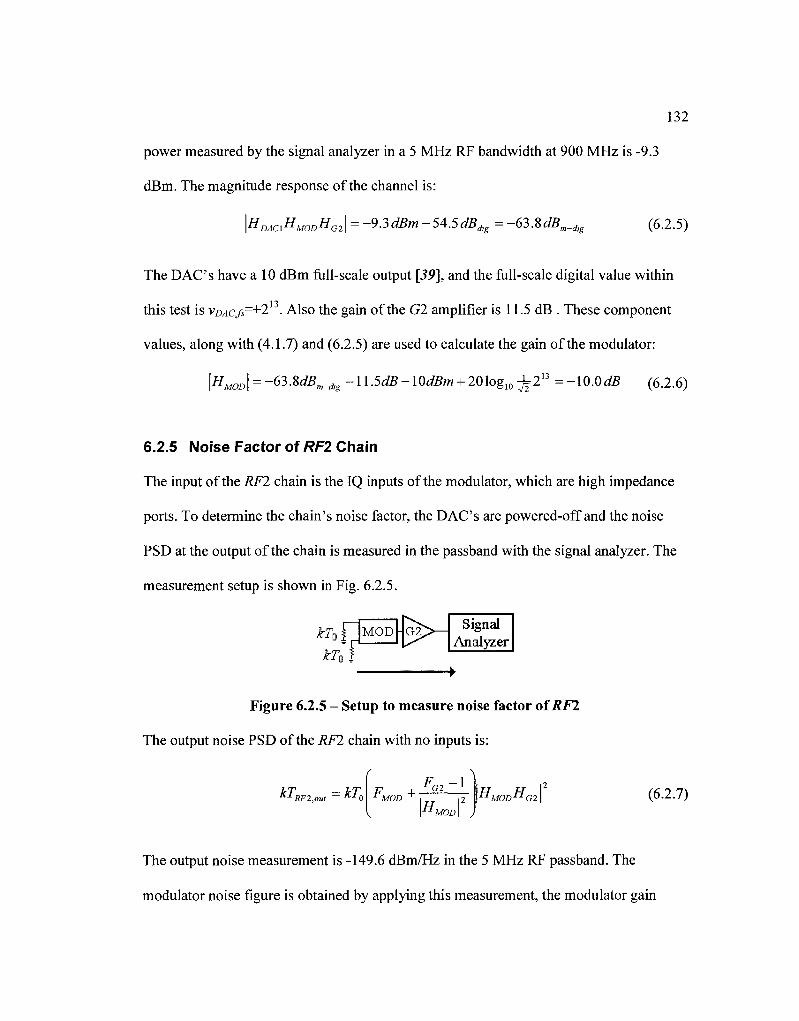
132
power measured by the signal analyzer in a 5 MHz RF bandwidth at 900 MHz is -9.3
dBm. The magnitude response of the channel is:
\HDAClHMODHG2\ = -9.3 dBm- 54.5 dBdlg = -63.8dBm_dig (6.2.5)
The DAC's have a 10 dBm full-scale output [39], and the full-scale digital value within
this test is vDAcfs=±2n. Also the gain of the G2 amplifier is 11.5 dB . These component
values, along with (4.1.7) and (6.2.5) are used to calculate the gain of the modulator:
\HMOD\ = -63-MB^ -n.5dB-l0dBm + 20log10^2u =-10.0dB (6.2.6)
6.2.5 Noise Factor of RFl Chain
The input of the RF2 chain is the IQ inputs of the modulator, which are high impedance
ports. To determine the chain's noise factor, the DAC's are powered-off and the noise
PSD at the output of the chain is measured in the passband with the signal analyzer. The
measurement setup is shown in Fig. 6.2.5.
£-rorjMODHG2;
mi Signal
Analyzer
• »
Figure 6.2.5 - Setup to measure noise factor of RFl
The output noise PSD of the RFl chain with no inputs is:
k-*RF2,out ~ k*0 F + 1 MOD T
FG2-\ M I2
11 MOD \
^MOD"G2\ (6.2.7)
The output noise measurement is -149.6 dBm/Hz in the 5 MHz RF passband. The
modulator noise figure is obtained by applying this measurement, the modulator gain
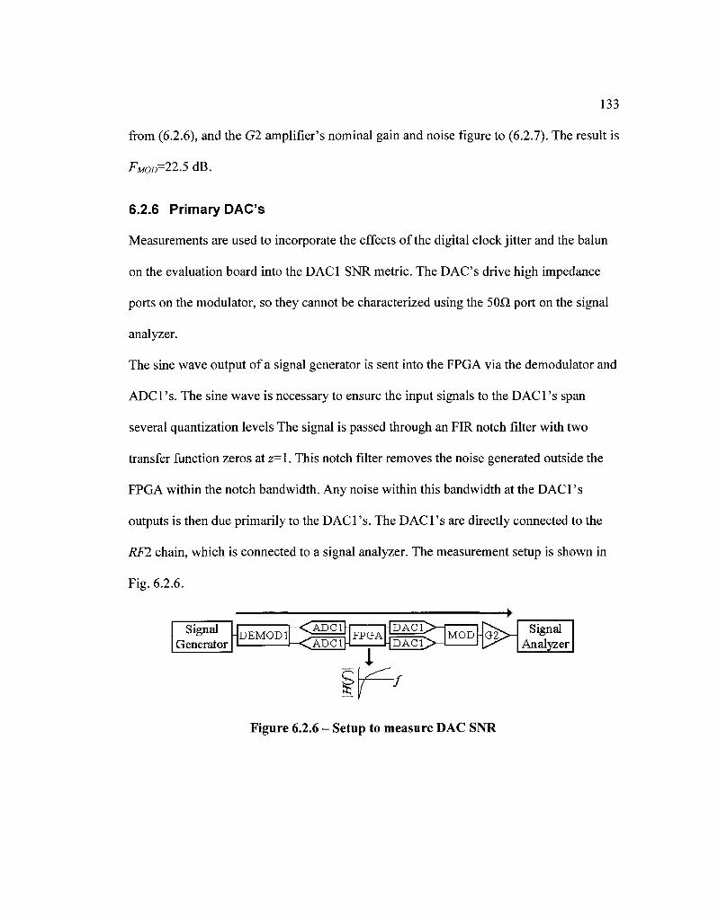
133
from (6.2.6), and the Gl amplifier's nominal gain and noise figure to (6.2.7). The result is
-^MO£I=22.5 dB.
6.2.6 Primary DAC's
Measurements are used to incorporate the effects of the digital clock jitter and the balun
on the evaluation board into the DAC1 SNR metric. The DAC's drive high impedance
ports on the modulator, so they cannot be characterized using the 50£1 port on the signal
analyzer.
The sine wave output of a signal generator is sent into the FPGA via the demodulator and
ADCl's. The sine wave is necessary to ensure the input signals to the DACl's span
several quantization levels The signal is passed through an FIR notch filter with two
transfer function zeros at z=\. This notch filter removes the noise generated outside the
FPGA within the notch bandwidth. Any noise within this bandwidth at the DAC1 's
outputs is then due primarily to the DAC1 's. The DAC1 's are directly connected to the
RF2 chain, which is connected to a signal analyzer. The measurement setup is shown in
Fig. 6.2.6.
•
Signal L Generator
DEMOD1 ADC1
ADC1 FPGA
| D A C 1 > ^
i DAC1
MOD Signal Analyzer
& " /
Figure 6.2.6 - Setup to measure DAC SNR

134
The only contribution to the noise PSD at the signal analyzer in the passband is expected
to be from the DAC's and RF2 chain. The digital notch filter removes most of the noise
from DEMODl and the ADCl's. The noise PSD in the passband at the signal analyzer is:
kT = • DACJs
SNRDACB \HRFl\ +kTo(FRF2-^}H. RF2] (6.2.8)
The SNRDAC term can be isolated in (6.2.8) since the following terms are already known:
• Hnn^lAdB (from Section 6.2.3)
• FRFI = 22.9 dB (from Section 6.2.5)
The value of kT0Ut in (6.2.8) is measured for various input frequencies from the signal
generator's. The 0 dBFS SNRDAC results are shown in Fig. 6.2.7.
300 920 940 960 980 1000 Input frequency (MHz)
Figure 6.2.7 - 0 dBFS SNR for both DACl's
The curves in Fig. 6.2.7 are used to estimate the 0 dBFS SNR for both DACl's to be 65.1
dB. The SNR from the DAC data sheets is specified for a few scenarios, the most
relevant being 74 dB for a clock frequency of 210 MHz, and an input frequency of 5
MHz [39]. The value from the data sheet does not include the evaluation board
components or clock jitter.
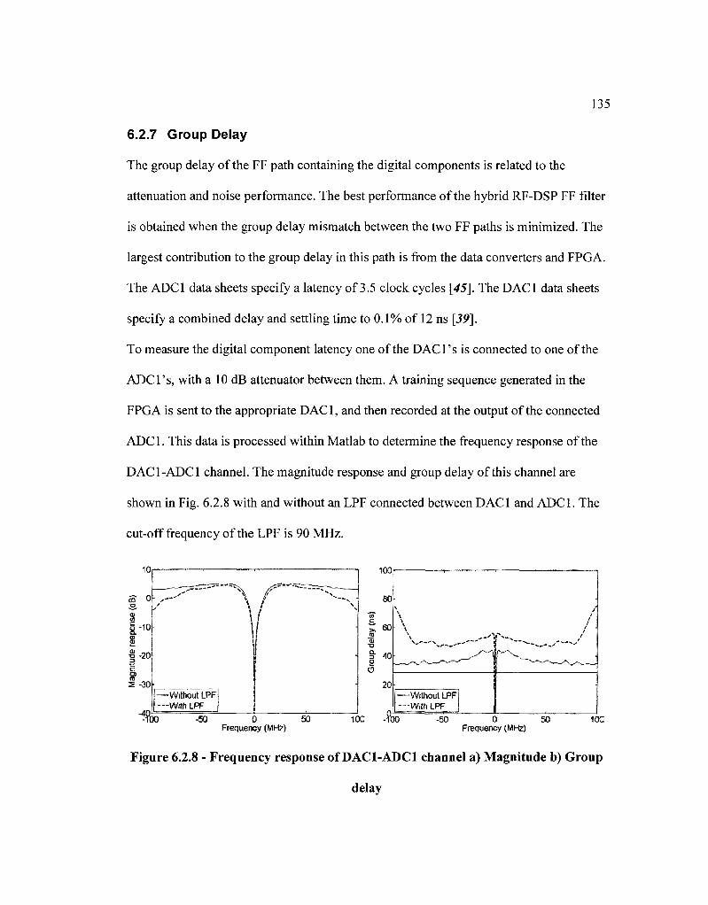
135
6.2.7 Group Delay
The group delay of the FF path containing the digital components is related to the
attenuation and noise performance. The best performance of the hybrid RF-DSP FF filter
is obtained when the group delay mismatch between the two FF paths is minimized. The
largest contribution to the group delay in this path is from the data converters and FPGA.
The ADC1 data sheets specify a latency of 3.5 clock cycles [45]. The DAC1 data sheets
specify a combined delay and settling time to 0.1% of 12 ns [39].
To measure the digital component latency one of the DACl's is connected to one of the
ADCl's, with a 10 dB attenuator between them. A training sequence generated in the
FPGA is sent to the appropriate DAC1, and then recorded at the output of the connected
ADC1. This data is processed within Matlab to determine the frequency response of the
DAC1-ADC1 channel. The magnitude response and group delay of this channel are
shown in Fig. 6.2.8 with and without an LPF connected between DAC1 and ADC1. The
cut-off frequency of the LPF is 90 MHz.
10
a -10 a. 1 * - 2 0
2 -30
1ft
\
—Without LPF —With LPF
100
"O § 40
O
00 -50 0 S3 Frequency (MHz)
10G -TOO -ft
Without LPF —Wi th LPF
-50 0 50 Frequency (MHz)
10C
Figure 6.2.8 - Frequency response of DAC1-ADC1 channel a) Magnitude b) Group
delay
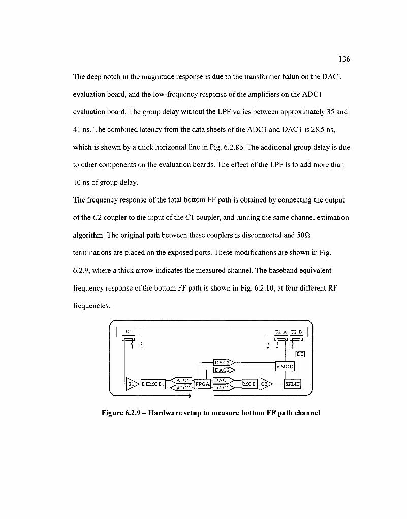
136
The deep notch in the magnitude response is due to the transformer balun on the DAC1
evaluation board, and the low-frequency response of the amplifiers on the ADC1
evaluation board. The group delay without the LPF varies between approximately 35 and
41 ns. The combined latency from the data sheets of the ADC1 and DAC1 is 28.5 ns,
which is shown by a thick horizontal line in Fig. 6.2.8b. The additional group delay is due
to other components on the evaluation boards. The effect of the LPF is to add more than
10 ns of group delay.
The frequency response of the total bottom FF path is obtained by connecting the output
of the C2 coupler to the input of the CI coupler, and running the same channel estimation
algorithm. The original path between these couplers is disconnected and 50Q.
terminations are placed on the exposed ports. These modifications are shown in Fig.
6.2.9, where a thick arrow indicates the measured channel. The baseband equivalent
frequency response of the bottom FF path is shown in Fig. 6.2.10, at four different RF
frequencies.
ci
T?
Sx DEMOD1 —<ADC1| - Q P C 1 |
n - | D A C 2 > -
DAC2~>-
FPGA DAC1 DAC1
C2 A C2B
rrrw P2
VMOD
MOD G2> SPLIT
"•
Figure 6.2.9 - Hardware setup to measure bottom FF path channel
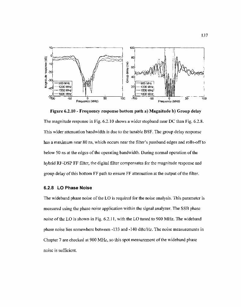
137
-SO O 50 Frequency (MHz)
-50 0 50 Frequency (MHz)
100
Figure 6.2.10 - Frequency response bottom path a) Magnitude b) Group delay
The magnitude response in Fig. 6.2.10 shows a wider stopband near DC than Fig. 6.2.8.
This wider attenuation bandwidth is due to the tunable BSF. The group delay response
has a maximum near 80 ns, which occurs near the filter's passband edges and rolls-off to
below 50 ns at the edges of the operating bandwidth. During normal operation of the
hybrid RF-DSP FF filter, the digital filter compensates for the magnitude response and
group delay of this bottom FF path to ensure FF attenuation at the output of the filter.
6.2.8 LO Phase Noise
The wideband phase noise of the LO is required for the noise analysis. This parameter is
measured using the phase noise application within the signal analyzer. The SSB phase
noise of the LO is shown in Fig. 6.2.11, with the LO tuned to 900 MHz. The wideband
phase noise lies somewhere between -133 and -140 dBc/Hz. The noise measurements in
Chapter 7 are checked at 900 MHz, so this spot measurement of the wideband phase
noise is sufficient.

138
:flfeilehf Phase NpiseyLoe Plot 1
*» PF 50 G AC I Z&F£ 1N~[
mmsm
1 1 2 9 Q O P M Mar 3 1 , 2 0 1 -
Carrier Freq 900.000015 MHz | Carrier Freq: 900.000015 MHz Noise Correction: Off
IFGam Low #Atten 10 dB Signal Tracking On
10 d Log
-70
BO
90
100
110
120
130
140
160
-160
I* _
R W | „ Ref -60dBc/Hz Carrier Power 1.61 dBm
, W Smoc Rav :hec
100 MHz Frequency Offset 100 MHz
1.00 MHz 10.0 MHz 100 MHz
-133.02 dE -136.39 dE -138 71 dE
cflHi cWi c/H:
-133 86dBc/Hz -136.80 dBcJHz -139 80dBcWz
i^D^aJH^^^^^
_
I >
V
Figure 6.2.11 - SSB phase noise of LO at 900 MHz
6.2.9 Summary of Bottom FF Path Characterization
The component values obtained in this section are required for the output noise
expression from Chapter 4. These component values are summarized in the following
four tables. The Hat term includes 1.35 dB of attenuation from the long coaxial cable
that connects the output of the filter to the signal analyzer. This cable loss was measured
with a vector network analyzer.

139
Table 6.3 - Component values for RFl
Variable FAMPX
HAMPI
FDEMODX
HDEMODX
PNWB
Value 1.03 dB 19.2 dB 45.3 dB 2.9 dB
-133 dBc/Hz
Comments Table 6.2 Table 6.2
Section 6.2.3 Section 6.2.3 Section 6.2.8
Table 6.5 - Values for digital terms
Variable PADCJS
B
SNRADC
SNRDAC
O-MULT
O-DAC
N
bhiULT
PDAC.fs
Value 15.3 dBm 100 MHz
64.3 dB 65.1 dB
2M
2 . 6
32
44
10 dBm
Comments Section 6.2.3
Digital clock is 200 MHz
Section 6.2.2 6.2.6
Digital filter specifics
Digital filter specifics
Digital filter specifics
Digital filter specifics
Data sheet [39]
Table 6.4 - Component values for RFl
Variable FAMPI
HAMPI
FMOD
HMOD
PNWB
Value 4.3 dB 11.5 dB 22.5 dB -10.0 dB
-133 dBc/Hz
Comments Table 6.2 Table 6.2
Section 6.2.5 Section 6.2.3 Section 6.2.8
Table 6.6 - Values for RF FF path
Variable Hcu Hc\c Hcu Hcic Hc3t HTOP
FJOP
Value -0.81 dB -10 dB -0.4 dB -20 dB
-2.25 dB 1
1
Comments Table 6.2 Table 6.2 Table 6.2 Table 6.2 Table 6.2
Small coaxial cable
Small coaxial cable
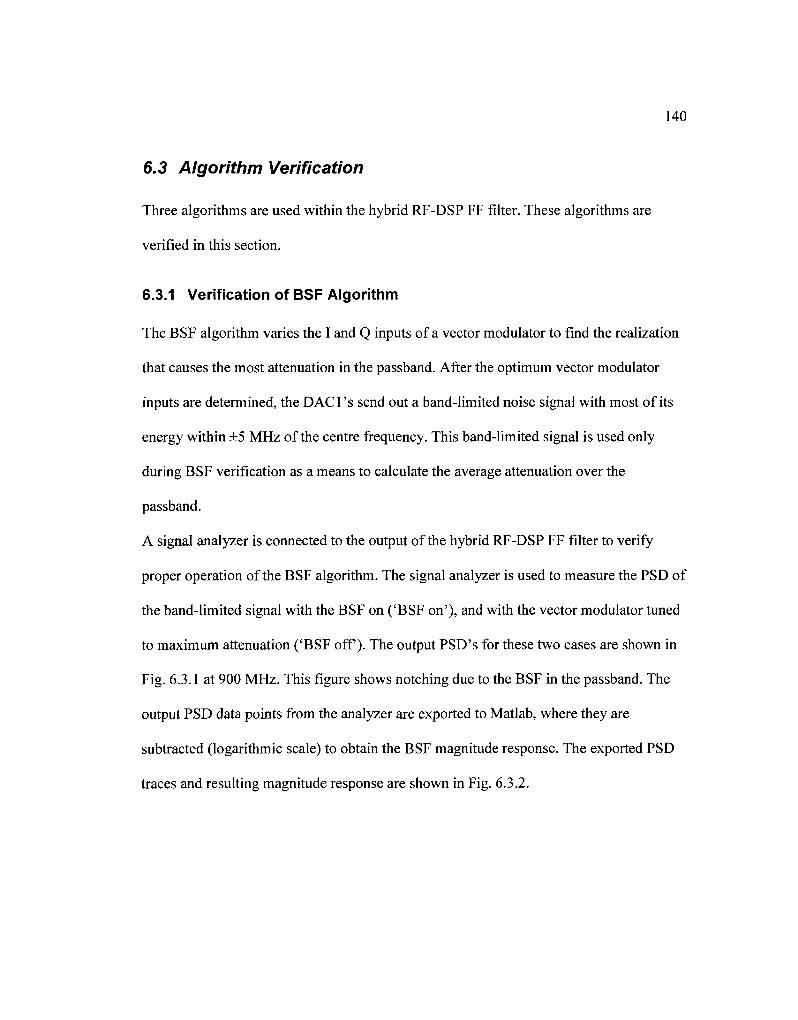
140
6.3 Algorithm Verification
Three algorithms are used within the hybrid RF-DSP FF filter. These algorithms are
verified in this section.
6.3.1 Verification of BSF Algorithm
The BSF algorithm varies the I and Q inputs of a vector modulator to find the realization
that causes the most attenuation in the passband. After the optimum vector modulator
inputs are determined, the DAC1 's send out a band-limited noise signal with most of its
energy within ±5 MHz of the centre frequency. This band-limited signal is used only
during BSF verification as a means to calculate the average attenuation over the
passband.
A signal analyzer is connected to the output of the hybrid RF-DSP FF filter to verify
proper operation of the BSF algorithm. The signal analyzer is used to measure the PSD of
the band-limited signal with the BSF on ('BSF on'), and with the vector modulator tuned
to maximum attenuation ('BSF off). The output PSD's for these two cases are shown in
Fig. 6.3.1 at 900 MHz. This figure shows notching due to the BSF in the passband. The
output PSD data points from the analyzer are exported to Matlab, where they are
subtracted (logarithmic scale) to obtain the BSF magnitude response. The exported PSD
traces and resulting magnitude response are shown in Fig. 6.3.2.
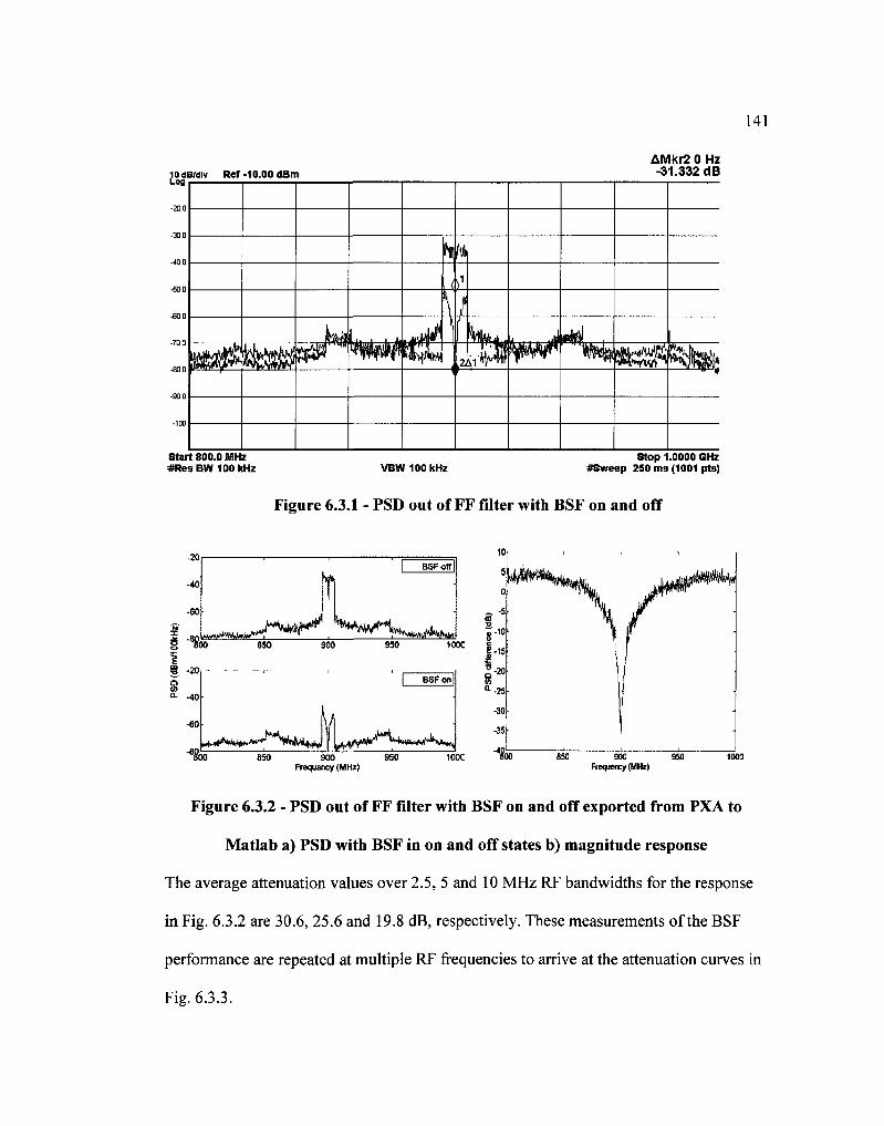
"lOdBJdlv Ref Log
•10.00 dBm
Start 800.0 MHz #ResBW100kHz
AMkr2 0 Hz -31.332 dB
n0 km ,Jb$ ptfT1 Ww
*IIMI
(
i**W Cfl
>1
/
HhU 2 ^ 1 * ^ Ups^ ' ' ^«SSK5taf r
VBWIOOkHz Stop 1.0000 GHz
#Sweep 250 ms (1001 pts)
Figure 6.3.1 - PSD out of FF filter with BSF on and off
10
5
0
_ -5
^w*w
o to
100C
-60
M M t ^ ^ * ^ ^ ^ * " ^ l ) ^ > r / ^ ^ w ^ " j ^
8-10
1-15
-35
V
850 900 950 Frequency (MHz)
850 900 350 Frequency (MHz)
Figure 6.3.2 - PSD out of FF filter with BSF on and off exported from PXA to
Matlab a) PSD with BSF in on and off states b) magnitude response
The average attenuation values over 2.5, 5 and 10 MHz RF bandwidths for the response
in Fig. 6.3.2 are 30.6, 25.6 and 19.8 dB, respectively. These measurements of the BSF
performance are repeated at multiple RF frequencies to arrive at the attenuation curves in
Fig. 6.3.3.
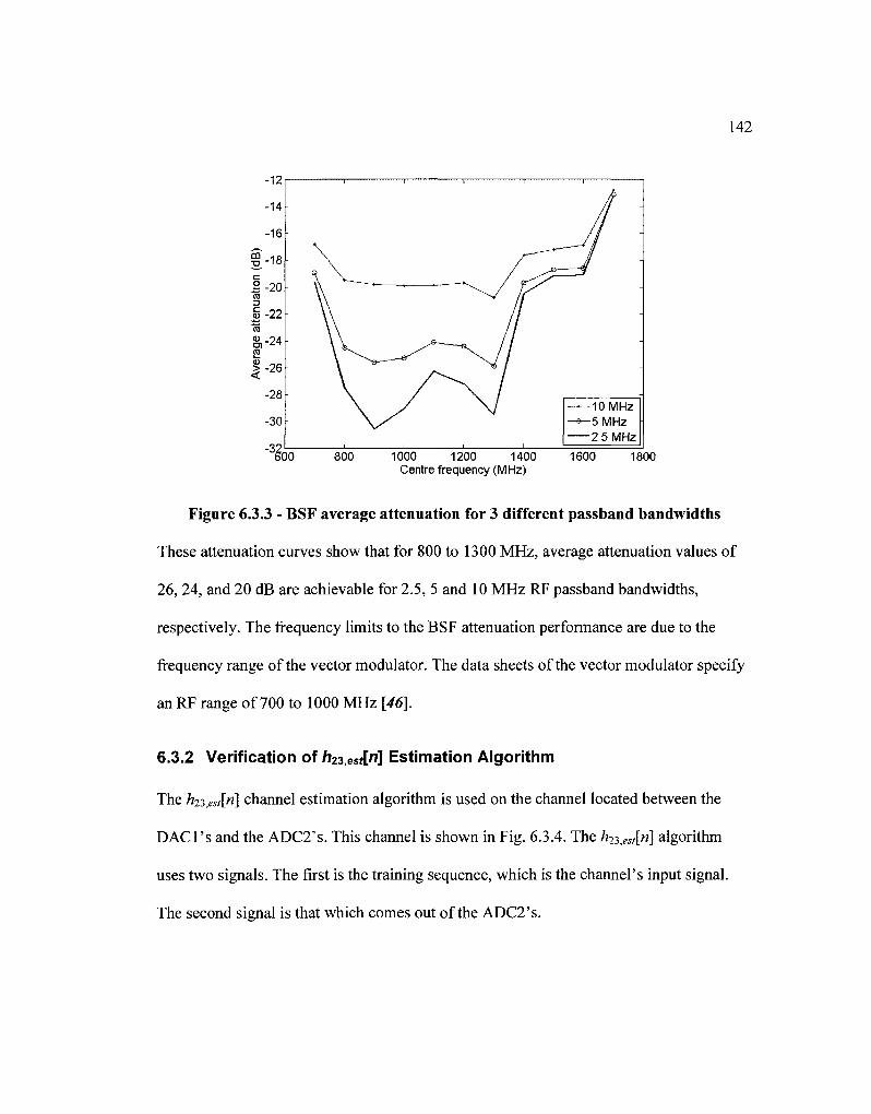
1000 1200 1400 Centre frequency (MHz)
1800
Figure 6.3.3 - BSF average attenuation for 3 different passband bandwidths
These attenuation curves show that for 800 to 1300 MHz, average attenuation values of
26, 24, and 20 dB are achievable for 2.5, 5 and 10 MHz RF passband bandwidths,
respectively. The frequency limits to the BSF attenuation performance are due to the
frequency range of the vector modulator. The data sheets of the vector modulator specify
an RF range of 700 to 1000 MHz [46].
6.3.2 Verification of h23,est[n] Estimation Algorithm
The h23,est[n] channel estimation algorithm is used on the channel located between the
DACl's and the ADC2's. This channel is shown in Fig. 6.3.4. The h2z,est[ri\ algorithm
uses two signals. The first is the training sequence, which is the channel's input signal.
The second signal is that which comes out of the ADC2's.

143
c i
IN nt C2-A C2-B C3
nJLnJ
BM Q D C I | -DEMODl Z. FPGA , .
I Q D C I H , I H D A C T > -
| D A C 2 > -
| — | D A C 2 > -
r\ VMOD
LO DIST
T CLOCK
DIST
LO TlOMHz REF
MOD SPLIT
HADC2>HLPFh
HADC2>JLPF" DEMOD2
= 3 J O U T
Figure 6.3.4 - Hardware prototype with h23[n] channel indicated
To verify proper operation of the /j23,«*["] channel estimation algorithm, the channel's
actual response is required. This response is not known, but is estimated using a software-
based technique and the channel's input and output signals. These signals are picked-off
the FPGA and transferred to Matlab. The channel's input signal is a training sequence
with a uniform PSD over the Nyquist bandwidth. The two picked-off signals are used to
find the channel response in the MMSE sense by calculating the corresponding FIR
Wiener filter. Approximately 65500 sequential samples are transferred from the FPGA
for the input and output signals. The FIR Wiener filter response from this software based
channel estimation is the 'Simulink' curve in Fig. 6.3.5. This result is obtained with the
hybrid RF-DSP FF filter operating at 1200 MHz. The steady-state solution of the FPGA
algorithm is also captured. The resulting magnitude response and group delay are the
'FPGA' curves in Fig. 6.3.5.
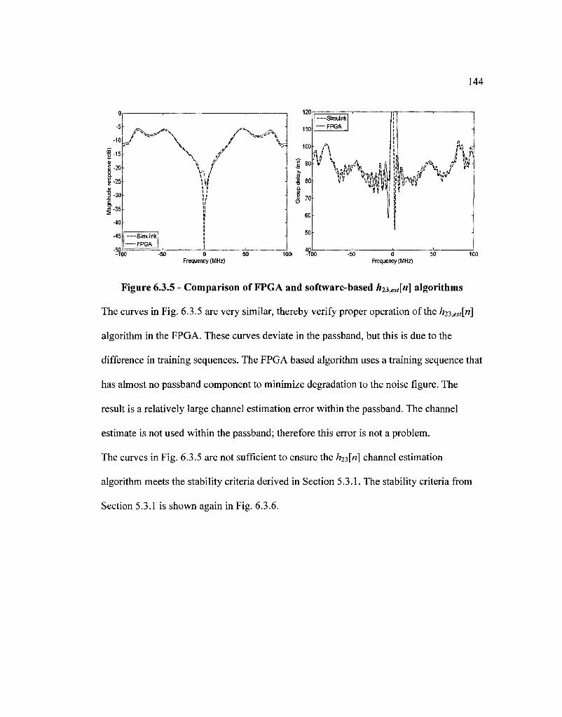
144
—Smdink > —FPGA !
•M -50 0 50 100 - f00~ -50 0 50 100 Frequency (MHz) Frequency (MHz)
Figure 6.3.5 - Comparison of FPGA and software-based /*23,es<[«] algorithms
The curves in Fig. 6.3.5 are very similar, thereby verify proper operation of the /?23,^[«]
algorithm in the FPGA. These curves deviate in the passband, but this is due to the
difference in training sequences. The FPGA based algorithm uses a training sequence that
has almost no passband component to minimize degradation to the noise figure. The
result is a relatively large channel estimation error within the passband. The channel
estimate is not used within the passband; therefore this error is not a problem.
The curves in Fig. 6.3.5 are not sufficient to ensure the feM channel estimation
algorithm meets the stability criteria derived in Section 5.3.1. The stability criteria from
Section 5.3.1 is shown again in Fig. 6.3.6.
-5
-10
| - 1 5 1)
Q.
£ -25
2-30-
| - 3 5 .
-40
-45
/v '-J
—Simulink FPGA
^ * ^ \ j
V / \f w
] I \ 1
., _ _ J
' " v w ^ \ '
-
-
110
100
1 $° % 80 a
70
60
50
O

145
Real<Vad)
Figure 6.3.6 - Stability criteria for main algorithm (from Section 5.3.1)
The value of ygract is defined in Section 5.3.1, and is repeated in (6.3):
I grad H23(z)
(6.3.1)
In this equation, H2Xerr(z) is the z-domain channel estimation error obtained by
subtracting the channel estimate, H23>est(z), from the actual channel response, / ^ ( z ) . A
specific channel estimate will have a different value of ygrad at each frequency point,
where z=exp(j2iifTs). Consider plotting an individual point in Fig. 6.3.6 for ygrad at each
frequency in the operating bandwidth, excluding the passband. The stability criterion is
then determined by the smallest circle, like those in Fig. 6.3.6, which surrounds all of the
plotted points. The stability criterion can be rearranged to represent a maximum limit on
HB^- The values of fiB and I are the adaptive algorithm step size and eigenvalue of the
filtered input signal (uest[n]) to the main digital filter. These values are introduced in
Chapter 5.
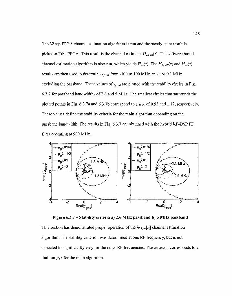
146
The 32 tap FPGA channel estimation algorithm is run and the steady-state result is
picked-off the FPGA. This result is the channel estimate, Hjz^stiz). The software based
channel estimation algorithm is also run, which yields Hniz). The Hn^st{z) and H2i{z)
results are then used to determine ygrad from -100 to 100 MHz, in steps 0.1 MHz,
excluding the passband. These values of ygracj are plotted with the stability circles in Fig.
6.3.7 for passband bandwidths of 2.6 and 5 MHz. The smallest circles that surrounds the
plotted points in Fig. 6.3.7a and 6.3.7b correspond to a / / ^ of 0.93 and 1.12, respectively.
These values define the stability criteria for the main algorithm depending on the
passband bandwidth. The results in Fig. 6.3.7 are obtained with the hybrid RF-DSP FF
filter operating at 900 MHz.
R e a « W Real<W Figure 6.3.7 - Stability criteria a) 2.6 MHz passband b) 5 MHz passband
This section has demonstrated proper operation of the h23,est[n] channel estimation
algorithm. The stability criterion was determined at one RF frequency, but is not
expected to significantly vary for the other RF frequencies. The criterion corresponds to a
limit on //gA for the main algorithm.
147
6.3.3 Verification of Main Algorithm
The purpose of this section is to demonstrate proper operation of the main algorithm for a
single realization of an input interference environment. The output PSD's with the hybrid
RF-DSP FF filter turned off and on are measured by a signal analyzer and are shown in
Fig. 6.3.8 and 6.3.9, respectively. Three large tones are visible in Fig. 6.3.8, each labelled
with a marker. When the filter is turned on and reaches steady-state, these three sinusoids
appear attenuated at the filter output, shown in Fig. 6.3.9. The attenuation values are
obtained by subtracting the marker values, which are shown below the PSD's in the
tables. The attenuation values are 38.2, 48.3 and 46.7 dB for the sinusoids at 926, 990 and
1015 MHz. The centre frequency of the filter is 950 MHz. These results demonstrate
proper operation of the main algorithm for a single realization. The next chapter reports
on more complex input interference scenarios.

PNO: Fast C^D T r i 9 ' F r e e R u n
IFGain Low Atten: 10 dB
Avg Type: Log-Pwr Avg|Hold>10/10
TRACE TYPE
1 2 3 4 5 t
S S N N N f
10dB/div RefO.OOdBm
100
20 0
-30 0
-40 0
500
-60 0
70 0
-BOO
-90 0
fiWff mm TITTP"
0
kiiiliu J WM\
1 02
. , . 1 ^ J
i-WP^f^w^pW"1 ]Wtp
o3
ff f ff IT W\Wff\ Start 850.0 MHz Stop 1.0500 GHz #Res BW 100 kHz VBW 100 kHz Sweep 76.3 ms (1001 pts)
1 | N I [ f l 926.0 MHz| -10.597 dBm[ 21 N I I f I 990.0 MHzl -5.633 dBm I 3| N | | f | 1.0150GHz| -8.907 dBm|
l ^ m • B ! l ^ ^ ^ ^ o
ad
Figure 6.3.8 - Filter output with all zero filter taps
PNO: Fast C^D T r i S ; F r e e R u n
IFGainiLow Atten- 10 dB
Avg Type: Log-Pwr Avg|Hold>10f10
TRACeh 2 3 4 5 ( TYPE A A W W f t W
i DET S S N N N I
10 dB/div Ref 0.00 d B m
-10 0
-20 0
300
400
-50 0
-BOO
-70 0
-BOO
-90 0
Star me
i&nrai
1[ ? 3
d I I
kXw l
S"#w I [iMflf
Mtm
<>1
fltai ^ wu
•|«|H
**4 *%
Jt IX \f
1
\
(#4rtK
a II
^HYH1!
o3
1 i I ith J^ "MI I I I "X.
1850 .0 MHz Stop 1.0500 GHz s BW 100 kHz V B W 100 kHz Sweep 76.3 ms (1001 pts)
N I f f [ 926.0 MHzl -48.783 dBm I N I | f I 990.0 MHzl -53.969 dBm N | | f | 10150GHz| -55.608dBm
^^^^mswmm^^^^ &
£*s
Figure 6.3.9 - Filter output with main algorithm in steady state
149
6.4 Hardware Prototype Summary
This chapter has introduced the hardware prototype and verified proper operation of the
three adaptive algorithms. Component values have been obtained for the analytical
expressions in Chapter 4 either from data sheets, or measurements. The following chapter
reports measurements of the hardware prototype for different filter realizations and input
interference scenarios.

7 Hardware Prototype Performance
The measured performance of the hardware prototype is reported in this chapter.
Narrowband input signals are used to demonstrate the filter's: frequency agility, handling
of dynamic inputs and near band attenuation performance. Wideband input signals are
used to determine how the attenuation performance is related to: the number of FIR filter
taps, group delay mismatch between the two FF paths, and the block size within the
adaptive algorithm. Additionally, the noise analysis from Section 4.1 is verified.
7.1 Measurement Setup
The hybrid RF-DSP FF filter is tested with several different input interference scenarios.
The outputs of several signal generators (Sig Gen) are combined, and then connected to
the input of the filter. Four Sig Gen outputs are combined using a 4-1 combiner. A
maximum of eight Sig Gen outputs are combined using two 4-1 combiners, and a 2-1
combiner to combine the outputs of the 4-1 combiners. The output of the filter is
connected to an Agilent PXA signal analyzer. The measurement setup is illustrated in
Fig. 7.1.1, where the details of the hybrid RF-DSP FF filter are omitted. Throughout this
chapter the digital clock frequency is fixed at 200 MHz, and the LO is varied over the
filter's operating range.
150
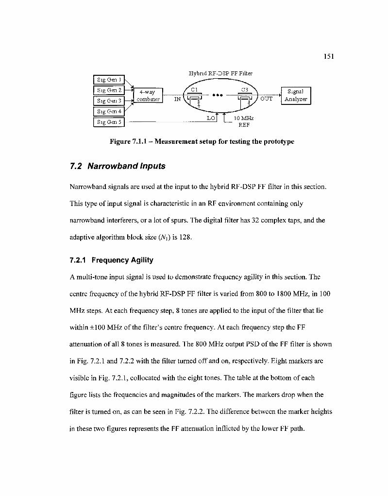
Hybrid RF-DSP FF Filter
L
C3 N
-—lJ / OUT ' Signal
Analyzer
Figure 7.1.1 - Measurement setup for testing the prototype
151
7.2 Narrowband Inputs
Narrowband signals are used at the input to the hybrid RF-DSP FF filter in this section.
This type of input signal is characteristic in an RF environment containing only
narrowband interferers, or a lot of spurs. The digital filter has 32 complex taps, and the
adaptive algorithm block size (N\) is 128.
7.2.1 Frequency Agility
A multi-tone input signal is used to demonstrate frequency agility in this section. The
centre frequency of the hybrid RF-DSP FF filter is varied from 800 to 1800 MHz, in 100
MHz steps. At each frequency step, 8 tones are applied to the input of the filter that lie
within ±100 MHz of the filter's centre frequency. At each frequency step the FF
attenuation of all 8 tones is measured. The 800 MHz output PSD of the FF filter is shown
in Fig. 7.2.1 and 7.2.2 with the filter turned off and on, respectively. Eight markers are
visible in Fig. 7.2.1, collocated with the eight tones. The table at the bottom of each
figure lists the frequencies and magnitudes of the markers. The markers drop when the
filter is turned on, as can be seen in Fig. 7.2.2. The difference between the marker heights
in these two figures represents the FF attenuation inflicted by the lower FF path.
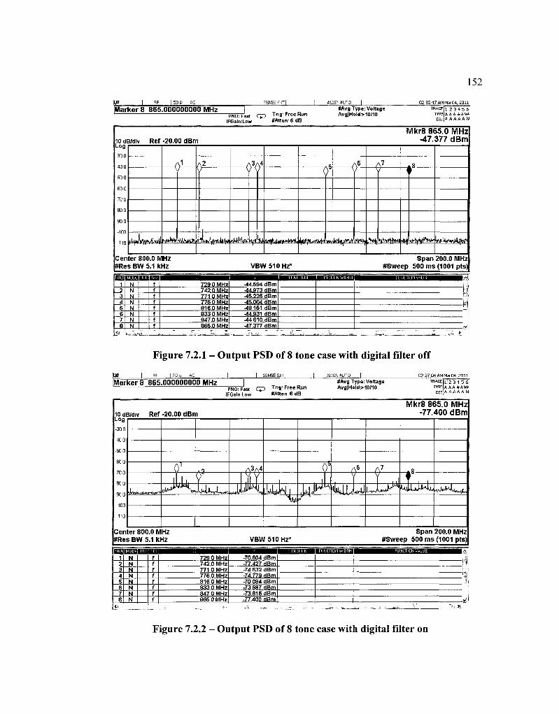
jye j I F [ S O P sc
[Marker 8 865.000000000 MHz SHMScE^j [
PNO:Fast C P Tr ig-Free Run IFGain:Low * A t t e r r 6 d B
ALIGP- AUTO | #Avg Type: Voltage Avg|Hold>10/10
02 35 47 AM Mar 04, 2011 TRACE
TYPE D£T
1 2 3 4 5 6 AAAfcAW A A A A A N
M k r 8 865.0 M H z lOdB/div Ref-20.00 dBtn -47 .377 d B m
300
400
50 0
60 0
70 0
80 0
90 0
•100
110 . rWjWIhrf
/\1
s*>. Wfc*lE
A2 v
I
/ \ 3 A 4
V y
nURn. u
c
7 A 6
v
k i «aLlia*>*vil, ikWkMVWW W k i W
V y
•V* Artl wiMin*
A 8
•
•MVtiW^^ UVvOklJW'
Center 800.0 MHz Span 200.0 MHz #Res BW 5.1 kHz VBW510HZ* #Sweep 500 ms (1001 pts)
M l 1 7 3 4 5 B 7 0
«
BIHB;
N
N N N N N N N
Ha 729 0 MHz 742 0 MHz 771 0 MH2 776 0 MHz 816.0 MHz 833 0 MHz 847.0 MHz 866.0 MHz
*JZJZ ,7 * " _ i*""_ "-JF I.
-44.594 dBm -44.973 dBm -45.226 dBm -45.004 dBm -48 151 dBm -44.931 dBm -44 610 dBm -47.377 dBm
^ \ »a "" " "" ~ iu "7* r \ ^ w.
^ ^ ™ H M ^ " " f ; n j j i
.7 ""7" ~ ™
~~ *w r TS >
Figure 7.2.1 - Output PSD of 8 tone case with digital filter off
I W | RF | 50 u AC
Marker 8 865.000000000 MHz 1 I SENSE EXT 1
PNO: Fast Q3 T r l 9 ' Free Run IFGain Low *Atten 6 dB
ALIGN A i r O |
tfAvg Type: Voltage Avg|Hold:>1(M10
02 37 04 AM Mar 0 4 , 2 0 1 1
TRACE TYPE
DEI
1|2 3 4 5 6 AAAA-AW A A A A A N
M k r 8 865.0 M H z iodB/di» Ref-20.00 dBm -77 .400 d B m
•30 0
400
•50 0
600
70 0
600
900
100
110
Cen
GBI 1 ? 3 4 S 6 7 8
«•
0' I ll I,
M ^ \
-•> 0 JsMX^Lvvln,
A 3 A 4
uj^y
M P%
i .JM/MI
\i
<)b
, I
,4.Fi / ^
/\6
Y 4i4J,*iJ
A?
v I J4 L v t l l * * ^ " ^
A 8
t I I ^LuWJl. W»*Hu4L
ter 800.0 MHz Span 200.0 MHz sBW5.1kHz VBW510HZ' #Sweep 500 ms (1001 pts)
Mil N N N N N N N N
IKHBB
;
729 0 MHz 742.0 MHz 771 0 MHz 776 0 MHz 816 0 MHz 833 0 MHz 847 0 MHz 865 0 MHz
•70.604 dBm -77.427 dBm -74 632 dBm -74.779 dBm -70 084 dBm -73 687 dBm -73.816 dBm -77.400 dBm
. , > , . 5 . w * -"" -K J - Z-
^ J
V
, : ^ ; » V ™ X. 6, * , * , V *Ji 51
Figure 7.2.2 - Output PSD of 8 tone case with digital filter on
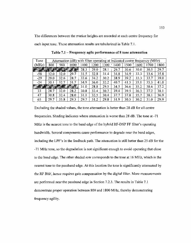
153
The differences between the marker heights are recorded at each centre frequency for
each input tone. These attenuation results are tabularized in Table 7.1.
Table 7.1 - Frequency agile performance of 8 tone attenuation
Tone (MHz)
%&WKk -58 -29 -24
33 47 65
Attenuation (dB) with filter operating at indicated centre frequency (MHz) 800
fife! 32.0 29.0 30.1
| 2 l . 0 | 28.7 30.8 29.7
900
32.0 32.6 32.7
m%„ 32.0 32.4 33.8
1000 27.0 29.7 28.7 31.7 26$ 28.2 28.0 29.3
1100 28.3 31.5 33.6 34.9 31.0 30.8 31.1 29.7
1200 29.0 32.8 34.2 36.0 28.8 32.4 32.5 31.2
1300 28.1 31.4 30.2 32.2 29.5 30.7 30.4 29.8
1400 29.7 34.8 38.9 40.7 34.5 39.4 37.7 31.9
1500 30.6 34.9 39.2 41.5 36.6 39.5 37.8 30.5
1600 30.0 33.3 33.3 35.1 35.2 36.3 35.7 30.2
1700 30.5 33.6 33.7 35.3 38.6 37.2 38.1 31.0
1800 29.7 35.8 39.0 41.0 37.2 38.1 36.9 29.9
Excluding the shaded values, the tone attenuation is better than 28 dB for all centre
frequencies. Shading indicates where attenuation is worse than 28 dB. The tone at -71
MHz is the nearest tone to the band edge of the hybrid RF-DSP FF filter's operating
bandwidth. Several components cause performance to degrade near the band edges,
including the LPF's in the feedback path. The attenuation is still better than 25 dB for the
-71 MHz tone, so the degradation is not significant enough to avoid operating that close
to the band edge. The other shaded row corresponds to the tone at 16 MHz, which is the
nearest tone to the passband edge. At this location the tone is significantly attenuated by
the RF BSF, hence requires gain compensation by the digital filter. More measurements
are performed near the passband edge in Section 7.2.3. The results in Table 7.1
demonstrate proper operation between 800 and 1800 MHz, thereby demonstrating
frequency agility.

154
7.2.2 Dynamically Changing Inputs
The hybrid RF-DSP FF filter handles a dynamic input interference scenario by adapting
the filter's notches in order to keep them collocated with the interferers. This section
demonstrates this behaviour by varying the input signal PSD in time. In order to report
this adaptive behaviour, the filter's output PSD's are shown before and after each time
the input signal is changed. Furthermore, the evolution of the filter's 32 taps is also
plotted with respect to time. The filter tap values are extracted from the FPGA in real
time using the SignalTapII tool within the QuartusII software. This tool is a virtual logic
analyzer.
The following measurements are obtained with the hybrid RF-DSP FF filter operating at
a centre frequency of 1225 MHz. The input signal frequencies are specified relative to
this centre frequency.
Initially the input signal consists of a tone at +73 MHz, and a 1 MHz wide signal at +28
MHz. This scenario is denoted 'Time 0'. An additional tone at -19 MHz is added to the
input signal at 'Time 1'. At 'Time 2' a tone at -24 MHz is added to the input. Lastly, at
'Time 3' the 1 MHz wide signal at +28 MHz is moved to -60 MHz. The output PSD's
with the digital filter turned off and on is shown in Fig. 7.2.3. This data is exported from
the signal analyzer. The PSD's in the right-side column represent the output after the
digital filter has converged. The purpose of this figure is to show the adaptive algorithm
is operating properly with each input scenario.
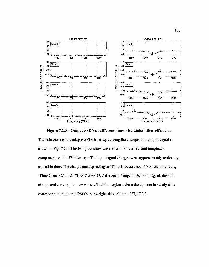
155
-40
-60
-80
-100
-40
Digital filter off Digital filter on
TimeO 3
IA»WIW ,I«WL 1150
»Ui~*.k»»fc*»Aj«HUJ***«w>tH«y»
1200 1250 ^W^MwtodvWWUodK*
1300
N" -60 X - * -80
in -100
E CO -o -40
D .60
°- -80
-100
-40
-60
-80
-100-
Time 1
iJ^AJvrtJtsJ*!***!!,****^^***^^,^.,)*^^***^
1150 1200 1250 1300
>Jifeferik!ha«4»L&£A«M«Jyu4c& 1200
?«/n«t^>«vS!^:-«fa^ 1300
Time 3
•iL^wi<4rfk, 1150
£A&£fe&&
1200 1250 Frequency (MHz)
1300 1150 1200 1250 Frequency (MHz)
1300
Figure 7.2.3 - Output PSD's at different times with digital filter off and on
The behaviour of the adaptive FIR filter taps during the changes to the input signal is
shown in Fig. 7.2.4. The two plots show the evolution of the real and imaginary
components of the 32 filter taps. The input signal changes were approximately uniformly
spaced in time. The change corresponding to 'Time 1' occurs near 10 on the time scale,
'Time 2' near 23, and 'Time 3' near 35. After each change to the input signal, the taps
change and converge to new values. The four regions where the taps are in steady-state
correspond to the output PSD's in the right-side column of Fig. 7.2.3.
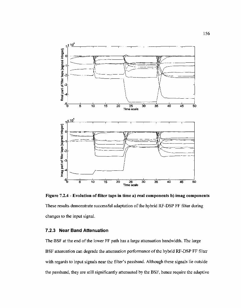
156
,x10
,x10
20 25 30 Time scale
40 45 50
Figure 7.2.4 - Evolution of filter taps in time a) real components b) imag components
These results demonstrate successful adaptation of the hybrid RF-DSP FF filter during
changes to the input signal.
7.2.3 Near Band Attenuation
The BSF at the end of the lower FF path has a large attenuation bandwidth. The large
BSF attenuation can degrade the attenuation performance of the hybrid RF-DSP FF filter
with regards to input signals near the filter's passband. Although these signals lie outside
the passband, they are still significantly attenuated by the BSF, hence require the adaptive

157
filter to compensate. A digital IIR stage is introduced in Section 3.1.3 to perform this
compensation, such that the adaptive FIR filter can be less constrained. The digital IIR
transfer function consists of one set of complex conjugate poles and a zero at z=l (in the
z-domain). The magnitude response of the IIR stage is shown in Fig. 7.2.5 for three cases.
The pole locations are different between the three cases. The digital IIR stage in the
FPGA requires three extra registers in the main path between the ADC1 's and DAC1 's.
These registers result in an additional 15 ns of group delay to the lower FF path.
_ 30 -m XI
w 2 Q
o
1 10
c Q. 0 E 8-10 c o>-20 a:
"??00 -50 6 50 100
Frequency (MHz)
Figure 7.2.5 - Gain compensation from IIR stage in FPGA
The hybrid RF-DSP FF filter is operated at 1000 MHz for the measurements in this
section. A single input signal is applied to the filter, which has a 1 MHz bandwidth and a
frequency offset that is varied from +2 to +15 MHz, relative to 1000 MHz. The average
power over the 1 MHz bandwidth is measured with the digital filter turned off and on.
The difference between the off and on results represents the FF attenuation. The
attenuation is shown in Fig. 7.2.6 for three different filter configurations: • IIR off: IIR stage performs no filtering. • IIR on: IIR stage has magnitude response corresponding to case iii in Fig. 7.2.5.
case i -case ii -case iii

158
• RF BSF off, IIR off: Vector modulator in RF BSF is set to maximum attenuation,
and the IIR stage performs no filtering.
35
30
^.25 CO
;c, c 2 0 o
115
< 10
5
°0 5 10 15
Input signal offset frequency (MHz)
Figure 7.2.6 - Attenuation of signals near passband
The results in Fig. 7.2.6 show the IIR stage does boost attenuation between 5 and 11
MHz, with the largest improvement at 8 MHz. The large difference between the RF-BSF
off curve and the IIR off curve proves that the RF-BSF causes the attenuation degradation
near the passband.
7.3 Wideband Inputs
This section demonstrates the attenuation performance of a single input with different
bandwidths. To keep the measurements consistent, the interferer is always located at 971
MHz, which is 21 MHz above the centre frequency of 950 MHz.
The output PSD's with the digital filter off and on are recorded by the signal analyzer for
one of the test cases reported in the following sub-sections, and are shown in Fig.
7.3.land 7.3.2. These figures show the input signal at 971 MHz has a finite bandwidth,
and is successfully attenuated by over 20 dB when the filter is turned on.

159
fct RF J53Q AC i | 1 SEMSEECT | AUGNAUTO I 09'14'32PMMar03, 2011
M a r k e r 1 9 7 1 . 6 0 0 0 0 0 0 0 0 M H z | »**aType:voltage ™»a:|i|234 5<: PNO- Fag CZ3 Trig: Free Run Avg|Hold> 10/10 TYPE A A-A-A-AW.
IFGain:High #Atten: 0 dB DEi lAAAAAr.
Mkr1 971.6 MHz 10dB/div Ref -30.00 dBm -54.348 dBm
m Wlrf* i l u\Wto
, 1 VHMpk VfWr^l T^fW irtHNw^
» i
t
^ W T " r^wv^irwwty l l , J jl^f^YV^
Center 950.0 MHz #Res BW 5.1 kHz VBW 510 Hr
Span 200.0 MHz #Sweep 500 ms (1001 pts)
Figure 7.3.1 - Output PSD with no FPGA output
w RF J?} £2 AC I I I SENSE EXT | ALIGN A. TO 09:13 52 PM Mar 03, 2011
M a r k e r 1 9 7 1 . 6 0 0 0 0 0 0 0 0 M H z I #Avg Type: Voltage T R A C E I ^ ^ £
PNO- Fasl G P Trig:FreeRun Avg|Hold>10/10 TYPE A A-ft A-A * IFGain:High *Atten: 0 dB M A * A A A •
MkM 971.6 MHz lOdB/div Ref-30.00 dBm -77.125 dBm
-40 0
-50 0
•60 0
-70 0
-BOO
-90 0
-100
-110
-120
• ^ T W ^ N A>v*+rV T ^ y T * / y v^
f AA ^ v \ ^
i \h/*vS "V
V1 i ^ U \
Center 950.0 MHz #Res BW 5.1 kHz VBW 510 Hz*
Span 200.0 MHz #Sweep 500 ms (1001 pts)
Figure 7.3.2 - Output PSD with filter in normal operating mode
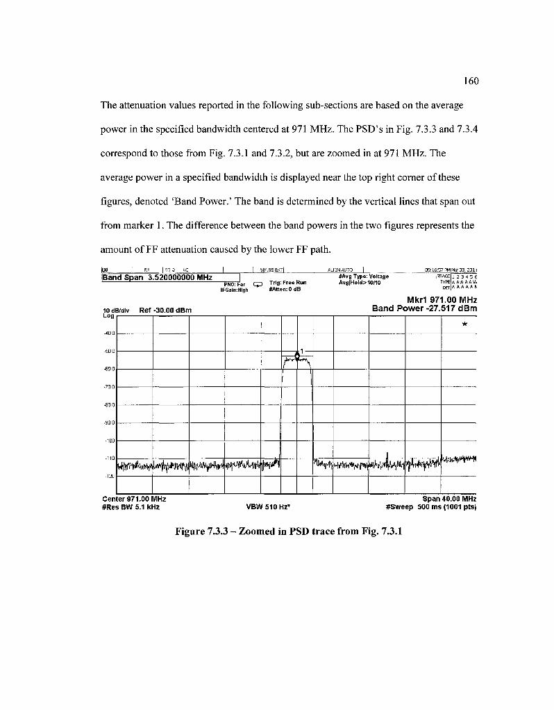
160
The attenuation values reported in the following sub-sections are based on the average
power in the specified bandwidth centered at 971 MHz. The PSD's in Fig. 7.3.3 and 7.3.4
correspond to those from Fig. 7.3.1 and 7.3.2, but are zoomed in at 971 MHz. The
average power in a specified bandwidth is displayed near the top right corner of these
figures, denoted 'Band Power.' The band is determined by the vertical lines that span out
from marker 1. The difference between the band powers in the two figures represents the
amount of FF attenuation caused by the lower FF path.
H» | R= | 50 J AC I SENSE EXT] ALIGN AUTO ] 09:16:57 PM Mar 03,2011
IBandSpan 3.520000000 MHZ | *Avg Type: Voltage TRACE! 2345e PHO- Far GD Trig: Free Run Avg|Hold:>W10 TYPE t t * M »
IFGain:High #Atten: 0 dB D E T A A A A A I *
MkM 971.00 MHz io<JB;div Ref-30.00dBm Band Power -27.517 dBm
1<#A'W ffijtfWH lillf^W^rVl IjN^WM^ |*i|tn
l«d
I
*Urt f4MiWVf*l I
«HV4H*I bi^ iV^
*
tejwniPy"^
Center 971.00 MHz #Res BW 5.1 kHz VBW510HZ*
Span 40.00 MHz #Sweep 500 ms (1001 pts)
Figure 7.3.3 - Zoomed in PSD trace from Fig. 7.3.1
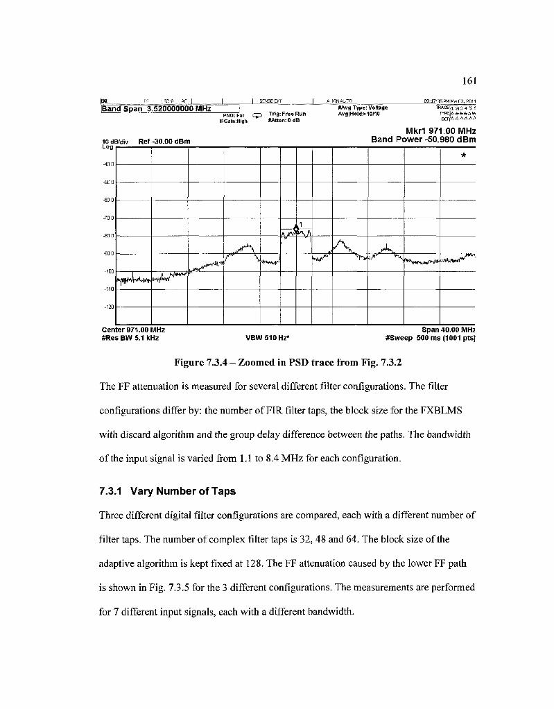
161
fM RF | sc a AC | Band Span 3.520000000 MHz
| | SENSE OCT 1
—PNOTFar c p T r lS: Free Run IFGain:High SAtten: 0 <JB
ALIGN ALTO
tfAvg Type: Voltage Avg|Hold:>10/10
09:17'35PMMar03,2011 TRACE
TYPE DET
1 2| 3 4 5 £
A A A A A N
10dBldiv Ref-30.00 dBm Log
Mkr1 971.00 MHz Band Power -50.980 dBm
nyflfivrAwr
V\ r \ ***ivf
/\J$ r\A 1
y - ^
*
A,, .A. rfV^
Center 971.00 MHz #Res BW 5.1 kHz VBW510HZ"
Span 40.00 MHz #Sweep 500 IDS (1001 pts)
Figure 7.3.4 - Zoomed in PSD trace from Fig. 7.3.2
The FF attenuation is measured for several different filter configurations. The filter
configurations differ by: the number of FIR filter taps, the block size for the FXBLMS
with discard algorithm and the group delay difference between the paths. The bandwidth
of the input signal is varied from 1.1 to 8.4 MFIz for each configuration.
7.3.1 Vary Number of Taps
Three different digital filter configurations are compared, each with a different number of
filter taps. The number of complex filter taps is 32, 48 and 64. The block size of the
adaptive algorithm is kept fixed at 128. The FF attenuation caused by the lower FF path
is shown in Fig. 7.3.5 for the 3 different configurations. The measurements are performed
for 7 different input signals, each with a different bandwidth.
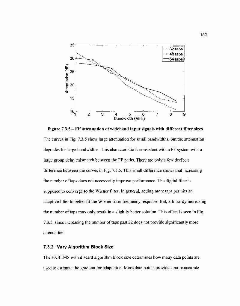
35
30
CO T3
c'25 .o
CD
I 20 CD
15
10
-
1 2 3 4 5
l
6 7
l
— 3 2 taps ^ - 4 8 taps — 6 4 taps
i
8 9 Bandwidth (MHz)
Figure 7.3.5 - FF attenuation of wideband input signals with different filter sizes
The curves in Fig. 7.3.5 show large attenuation for small bandwidths, but the attenuation
degrades for large bandwidths. This characteristic is consistent with a FF system with a
large group delay mismatch between the FF paths. There are only a few decibels
difference between the curves in Fig. 7.3.5. This small difference shows that increasing
the number of taps does not necessarily improve performance. The digital filter is
supposed to converge to the Wiener filter. In general, adding more taps permits an
adaptive filter to better fit the Wiener filter frequency response. But, arbitrarily increasing
the number of taps may only result in a slightly better solution. This effect is seen in Fig.
7.3.5, since increasing the number of taps past 32 does not provide significantly more
attenuation.
7.3.2 Vary Algorithm Block Size
The FXBLMS with discard algorithm block size determines how many data points are
used to estimate the gradient for adaptation. More data points provide a more accurate
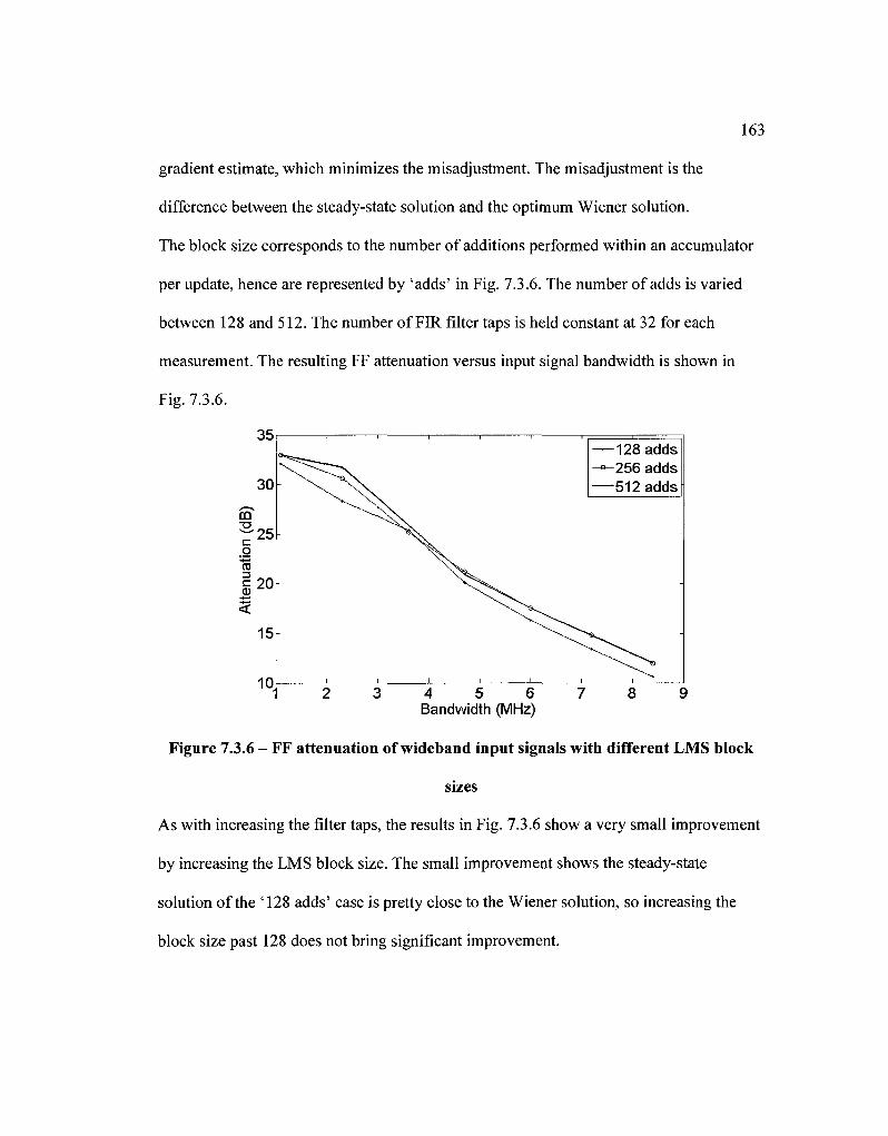
163
gradient estimate, which minimizes the misadjustment. The misadjustment is the
difference between the steady-state solution and the optimum Wiener solution.
The block size corresponds to the number of additions performed within an accumulator
per update, hence are represented by 'adds' in Fig. 7.3.6. The number of adds is varied
between 128 and 512. The number of FIR filter taps is held constant at 32 for each
measurement. The resulting FF attenuation versus input signal bandwidth is shown in
Fig. 7.3.6.
35
30-
25 CO
o
c 20
15
10
-
2 i
3 4 5 i
6 7
— 128 adds -*-256 adds —512 adds
8 9 Bandwidth (MHz)
Figure 7.3.6 - FF attenuation of wideband input signals with different LMS block
sizes
As with increasing the filter taps, the results in Fig. 7.3.6 show a very small improvement
by increasing the LMS block size. The small improvement shows the steady-state
solution of the ' 128 adds' case is pretty close to the Wiener solution, so increasing the
block size past 128 does not bring significant improvement.
164
7.3.3 Vary Group Delay
The last parameter varied with a single wideband input is the group delay difference
between the FF paths. The group delay of the lower FF path, excluding the registers
within the FPGA, is reported in Section 6.2.7. The registers within the FPGA increase the
group delay between the ADCl's and DACl's. The number of registers within the FPGA
is equal to four for the results reported in the two previous sections, excluding the IIR
stage results. This is the fewest number of registers allowable for timing reasons. The
digital clock runs at 200 MHz, so these registers contribute 20 ns of group delay to the
lower FF path.
The wideband attenuation of three filter configurations is measured and the results are
shown in Fig. 7.3.7. In this figure the 'no extra delay' curve represents the case with four
registers in the FPGA. Two extra registers are added between the ADCl's and DACl's in
the FPGA for the 'Delay added to lower path' curve. The other curve is obtained by
adding 7.8 metres of RG400 coax to the upper FF path. This length of cable has
approximately 37 ns of group delay. Also for this configuration, the number of registers
in the FPGA is equal to the minimum value of four. In all three configurations the
number of filter taps is 32, and the LMS block size is 128.

165
35
30
t 2 5
I 20 CO
CD
10
1
- ^ N o extra delay -*-Delay added to lower path —Delay added to upper path
4 5 6 Bandwidth (MHz)
8
Figure 7.3.7 - FF attenuation of wideband input signals with different group delay
The results of Fig. 7.3.7 show the additional registers in the lower FF path slightly
degrade the attenuation performance. The difference between these curves would be
larger if the group delay mismatch between the two FF path in the 'no extra delay' case
was much smaller. The delay added to the upper path shows a significant improvement in
the attenuation performance for a wideband input. This result is consistent with a FF
architecture where the group delay mismatch between the two paths is decreased. This
improved case shows the hybrid RF-DSP FF filter can adequately attenuate wideband
input signals when group delay is added to the upper FF path.
7.4 Noise Analysis Verification
The output noise PSD expression is derived in Section 4.1. This expression is checked
against measured results for several filter realizations. In the following measurements the
BSF is removed due to the poor linear performance of the vector modulator. Also, C\ is
replaced with a 20 dB directional coupler. The output noise is larger without the BSF,
thereby permitting a more accurate measurement. An accurate measurement serves the
greater purpose of this section, which is to validate the merger of RF and digital noise
analyses.
7.4.1 Expected Output Noise
The component values required for the output noise expression are listed in the four
tables in Section 6.2.9. These components values are specific to the hardware prototype.
The component values from these four tables are used to determine the magnitude and
noise factor expressions required by (4.1.1). The expression for each term is derived in
Section 4.1. The numerical value for each term, along with the corresponding equation
number from Section 4.1 is summarized below in Table 7.2. The noise factor terms for
RFl and RF2 in Table 7.2 do not include the noise due to mixing of the wideband phase
noise with the input signals. This noise is included in the expected noise results in the
following section.
Table 7.2 - Noise and magnitude terms for (4.1.1)
Term
FRFI
\HRFI\
FRF2
\HRF2.\
FDIG
\HDIG\
Derived equation (4.1.2) (4.1.2) (4.1.3) (4.1.3) (4.1.28) (4.1.6)
Numerical result (linear) 408.6 162.2 194.7
1.4 3.16xl05+1.72xl0y/|i/CSp|2
6.87xlO-u|//Z3SP|2
7.4.2 Measured Versus Expected Output Noise
The output noise PSD of the hardware prototype is measured in a 5 MHz passband for
different filter realizations and input signals. The output noise PSD is averaged over the
passband, excluding a small bandwidth centered at the centre frequency. The small
167
bandwidth at the centre frequency is omitted so the noise measurement does not include
LO-RF leakage from the modulator. This detail is shown in Fig. 7.4.1, which is a
zoomed-in screen capture from the signal analyzer for one of the noise PSD
measurements.
ALI6fJAUTO_
Avg Type: Pwr(RMS) PNO: Far CD Trig: Free Run
IFGain:Low SAtten: 6 dB
TRACE)! 2 3 4 5 ( TYPE I WvtnrVvWiAn DEI A N N N N I
10 dBfdiv Ref -34.00 dBm Log
Center 900.000 MHz #Res BW 51 kHz VBW 5.1 kHz'
Span 10.00 MHz #Sweep 5.00 s (1001 pts)
11 N f 898.68 MHz -127.10 dBmfHz Band Density 2.352 MHz -127.21 dBmfHz 2 N fB01.31MHz -126.66 dBm/Hz Band Density 2.375 MHz •126.31 dBmfHz
Figure 7.4.1 - Average noise PSD measurement over 5 MHz RF passband at 900
MHz
The derived noise expression is compared with the measured noise PSD in the passband
for two different input interference environments. For each of these two cases the number
of bits used by the ADC's and DAC's is varied. For each variation the average PSD in
168
the passband, and the average magnitude response of the digital filter are recorded. The
centre frequency is 900 MHz for both cases.
The output PSD's for both cases with the digital components turned off are shown in the
top row of Fig. 7.4.2. Significant interferer attenuation can be seen for both cases in the
figures in the bottom row, which is the measured PSD's with the filter turned on. The
details of the input interferers are summarized in Table 7.3.
Case i - Filter Off Case n - Filter Off
1000
850 900 950 Frequency (MHz)
1000
1000
850 900 950 Frequency (MHz)
1000
Figure 7.4.2 - Output PSD with filter on and off for both cases
Table 7.3 - Input interferers for both cases
Interferer ID
1 2 3 4
Freq (M
case i 845 880 923 966
uency Hz)
Hsase ii " 153 "
837, 916 921
Banc
case i CW 3.5 CW 1.5
Iwidth [Hz)
ease ijg 1 . 5 ^%
\A C W *,A
CW ' 3.5
Power (dBm)
case i -32.2 -31.8 -34.7 -32
case ii -3TT8 -32.2 -34.5 -32.4
The expected SNR's of the data converters are modified from those in Table 6.5 when the
number of bits used is less than the nominal 14. The modification accounts for the
additional quantization noise. The measured and expected noise results are shown in Fig.
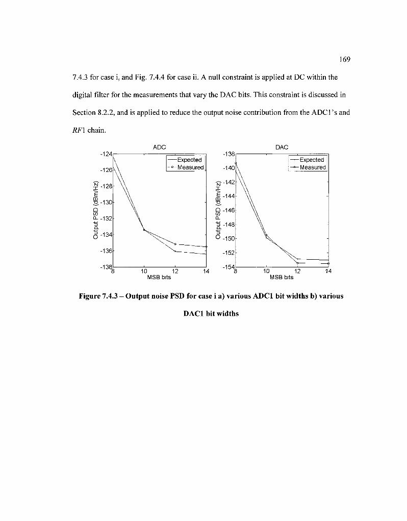
169
7.4.3 for case i, and Fig. 7.4.4 for case ii. A null constraint is applied at DC within the
digital filter for the measurements that vary the DAC bits. This constraint is discussed in
Section 8.2.2, and is applied to reduce the output noise contribution from the ADCl's and
RF\ chain.
ADC DAC
10 12 MSB bits
N IE E m 33.
D CO Q.
^Expected Measured
10 12 MSB bits
14
Figure 7.4.3 - Output noise PSD for case i a) various ADO bit widths b) various
DAC1 bit widths

ADC DAC
—Expected - « - Measured
-
~-&—-10 12 V
MSB bits 10 12
MSB bits 14
Figure 7.4.4 - Output noise PSD for case i a) various ADO bit widths b) various
DACl bit widths
The output noise PSD depends on the average magnitude response of the digital filter
over the passband. This response does not significantly vary when the number of bits
used by the data converter changes. The average magnitude response of the digital filter
in the passband is summarized in Table 7.4 for both cases. In this table \Hosp{fp)\ is
significantly lower when the DAC bits are varied. This lower value is due to the DC null
constraint mentioned above.
Table 7.4 -Average magnitude response of digital filter in noise measurements
Measurement
Vary ADC bits Vary DAC bits
\HDSP{fp)\ (dB) case i 109.1 88.7
case ii 112.4 100.1
The curves in Fig. 7.4.3 and Fig. 7.4.4 show a good match between predicted and
measured performance. The output noise contribution from RF\, RF2, the ADCl's and
DACl's are shown in Fig. 7.4.5 for the same data points on the 'Expected' curve in Fig.
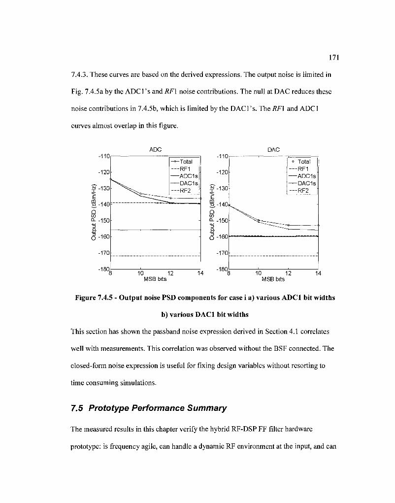
7.4.3. These curves are based on the derived expressions. The output noise is limited in
Fig. 7.4.5a by the ADCl's and RFl noise contributions. The null at DAC reduces these
noise contributions in 7.4.5b, which is limited by the DACl's. The RFl and ADCl
curves almost overlap in this figure.
ADC DAC -110
-120
N -130
1-140 Q CO
o- -150
O "160
-170
-180,
-
^ T o t a l —RF1 —ADC1s —DAC1s —RF2
-
"
-110
-120
N -130
§3-140. D CO
a- -150 "3 c±
§-160
-170
10 12 MSB bits
14 -180,
•
^ T o t a l — RF1 —ADC1s —DAC1s — RF2
-
8 10 12 MSB bits
14
Figure 7.4.5 - Output noise PSD components for case i a) various ADCl bit widths
b) various DAC1 bit widths
This section has shown the passband noise expression derived in Section 4.1 correlates
well with measurements. This correlation was observed without the BSF connected. The
closed-form noise expression is useful for fixing design variables without resorting to
time consuming simulations.
7.5 Prototype Performance Summary
The measured results in this chapter verify the hybrid RF-DSP FF filter hardware
prototype: is frequency agile, can handle a dynamic RF environment at the input, and can
172
attenuate narrowband and wideband interferers. Based on the different filter
configurations measured, it appears the most significant performance improvement is
obtained by minimizing the group delay mismatch between the two FF paths.

8 Conclusions and Discussions
Observations made during the theoretical analyses, simulations and measurements have
generated ideas for improvement of the hardware prototype and of the general analyses of
the filter. These ideas are discussed below.
8.1 First Order Approximations
Some generalizations regarding the dynamic range and group delay are made in this
section. The results are useful for first order approximations.
8.1.1 Dynamic Range
The dynamic range of the hybrid RF-DSP FF filter is limited to that of the FF path
containing the digital components. The noise analysis from Section 4.1 showed the noise
contribution of the components preceding the DACl's can be insignificant if the digital
filter is constrained to exhibit notches over the passband. One set of conditions were
determined to achieve a 1 dB noise figure for the hybrid RF-DSP FF filter in Section
4.1.4. The noise due to the DAC's dominated the noise factor (FFF) from the components
in the lower FF path, as the noise factor allocations were: FFP]RFI=0.01, FFFlRF2=0.0l,
FFPIADC=0.00\, FfF\DACf::0.\5. A typical PSD resulting from a single interferer is shown in
Fig. 8.1.1 between the DAC's and C2. Only the noise generated by the DAC's is shown
in the figure.
173
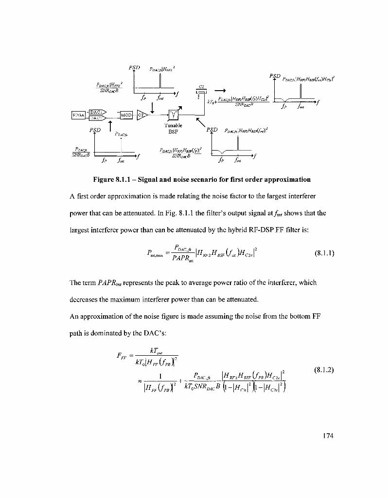
P2P PDACAHBFI?
PDACJS Wam\ SNRDACB
•f PoAC.fi \^RF2^Bsdfmt)^C2c\
{ D A C T > -
{ D A C T > -MOD
PSD 1
fp fail
HM—jx
>/ L n w0+
PDAC/1 WimHBSi{fp)Hc2c\
SNRDACB fp flM V
PpACfi SNRBACB
PDACJS
Tunable BSF
\ °%P PDAC/S Wmn^Bsiffrt.
fp fml -v PpACfi WsFiHBsdfp)\
SMRMCB ,//> •/«" -V
Figure 8.1.1 - Signal and noise scenario for first order approximation
A first order approximation is made relating the noise factor to the largest interferer
power that can be attenuated. In Fig. 8.1.1 the filter's output signal at/„, shows that the
largest interferer power than can be attenuated by the hybrid RF-DSP FF filter is:
p 1DAC.fi
PAPIL, \ H RF2HBSF\fmt)H> C2c\ (8.1.1)
The term PAPRint represents the peak to average power ratio of the interferer, which
decreases the maximum interferer power than can be attenuated.
An approximation of the noise figure is made assuming the noise from the bottom FF
path is dominated by the DAC's:
F -1 FF
kT„.
**0 \HFF \JPB j |
1 DAC.fi \"RF2^BSF \JPB )"C2C |
\HFF{fPBt ^o^^(i-|i/„,rii-i^i2)
(8.1.2)
- + -
174
The maximum input power (Pm) that the hybrid RF-DSP FF can handle is calculated by
de-embedding (7) to the filter's RF input. The expression for P,„ is substituted into the
noise factor approximation in (8.1.2) to get:
HBSF\fp) FM*
PmPAPRmi
\HFF\fp\ kT0SNRDACB " BSF Umt)
(8.1.3)
The expression in (8.1.3) is the first order approximation that relates the noise factor
(FFF) to the maximum input power (P,„). In this equation the term \HFF(fp)\ is the
magnitude response of the thru ports of the three directional couplers, and B is half the
digital clock frequency. The magnitude of the BSF in (8.1.3) is the combined response of
the RF BSF and digital gain compensation stage, which was introduced in Section 3.1.3.
The approximation in (8.1.3) is useful to determine the required SNR for the DAC's, and
if a digital gain compensation stage is required for the BSF given a specific Pm, PAPRml,
Fppifp), and RF operating bandwidth of the filter (2B). The approximation is valid when
the RF and analog components are designed for low noise, and the digital filter is
constrained to exhibit notches over the passband.
8.1.2 Group Delay
Attenuation performance of the hybrid RF-DSP FF filter was shown to strongly depend
on the group delay mismatch between the two FF paths. Adding filter taps and increasing
the amount of data used by the adaptive algorithm were found to only slightly improve
performance. This behaviour indicates the digital filter has no problem converging to the
175
Wiener solution for a given group delay mismatch. But, the MMSE of the Wiener
solution decreases with a decreasing group delay mismatch.
The z-spectrum at the output the hybrid RF-DSP FF filter is given for the case where the
digital filter is equal to the Wiener solution in (8.1.4). This equation is derived from
(4.2.5), (4.2.8), (4.2.9) and Fig. 4.2.3b. The z-spectrum of the input signal is Sxx{z).
S(z) = S„(z)HFF(z)HU U*) GA4
.D H'2{z) H[{z)
, \H;(±)\ Z-D HI'(±)\ I\DH';(\) X(J..Cr.. -T *GJr^rG) K®
„\rt\H'2{z) D
1 ^vy
"X,H[{z)
(8.1.4)
Recall from Section 4.2.2 that the value of D is the nominal delay from H2(z)/Hi(z). This
value is the group delay mismatch between the FF paths in the discrete-time domain. A
new term is introduced to simplify the expression in (8.1.4):
*M=|g«.W (8.1.5)
Both the numerator and denominator terms from (8.1.5) are minimum phase, therefore
K(z) is minimum phase. This minimum phase property means than k[n] is causal. The
expression from (8.1.4) is simplified using (8.1.5):
176
S„(z) = a'M^D-\K(z)zDl}x{K'{z)z°-\K'(z)zDl} (8.1.6)
The {K(z)zD-[K(z)zD]+} factor is converted into the discrete time domain in (8.1.7) to
demonstrate the effect of group delay mismatch on attenuation bandwidth.
IZT{K(Z)ZD -[K(Z)ZD\] = k[n + D]-k[n + D]u[n] (8.1.7)
If there was no group delay mismatch between the two FF paths, then D in (8.1.7) would
be zero. If D=0, then since k[n] is causal, the subtraction on the right side of (8.1.7)
would also be zero (ie. &[«]*/[«]=&[«]). For the Z)=0 case, large attenuation of the input
signal occurs, and there is no limit on the attenuation bandwidth.
When D>0, then the first D terms in k[n] are not subtracted in (8.1.7); therefore the
subtraction on the right side yields a non-zero value. As D increases, so does the number
of leading terms in k[n] that are not subtracted in (8.1.7).
As a first order approximation, let K(z) have a third-order low-pass Chebyshev type I
response with the cut-off frequency denoted byfc. This response is an approximation of a
single input signal with an RF bandwidth of 2fc. The magnitude squared response from
(8.1.7) is shown in Fig. 8.1.2 for different values of group delay mismatch (D), and input
signal bandwidth. The frequencies in the legend refer to the RF bandwidth of the
Chebyshev response, which corresponds to 2fc. The attenuation is proportional to the
magnitude squared response, so this figure is useful in determining how much the
attenuation performance will improve or degrade by changing the FF group delay
mismatch.
177
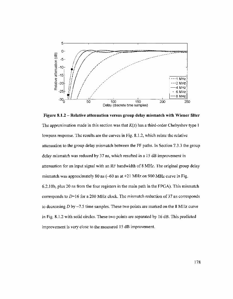
)i i n > \ i i i i ' 'i 0 50 100 150 200 250
Delay (discrete time samples)
Figure 8.1.2 - Relative attenuation versus group delay mismatch with Wiener filter
The approximation made in this section was that K(z) has a third-order Chebyshev type I
lowpass response. The results are the curves in Fig. 8.1.2, which relate the relative
attenuation to the group delay mismatch between the FF paths. In Section 7.3.3 the group
delay mismatch was reduced by 37 ns, which resulted in a 15 dB improvement in
attenuation for an input signal with an RF bandwidth of 8 MHz. The original group delay
mismatch was approximately 80 ns (-60 ns at +21 MHz on 900 MHz curve in Fig.
6.2.10b, plus 20 ns from the four registers in the main path in the FPGA). This mismatch
corresponds to D=\6 for a 200 MHz clock. The mismatch reduction of 37 ns corresponds
to decreasing D by -7.5 time samples. These two points are marked on the 8 MHz curve
in Fig. 8.1.2 with solid circles. These two points are separated by 16 dB. This predicted
improvement is very close to the measured 15 dB improvement.
178
8.2 Improvements and Future Work
Several improvements are suggested in these sections that were not incorporated into the
hardware prototype. These improvements can be incorporated when the hardware
prototype evolves into an integrated solution.
8.2.1 Equalizing ADC's and DAC's
Since the hardware prototype is built with evaluation boards, connectorized components,
and a lot of coaxial cable, there are variations between I and Q paths near the ADC1 's,
ADC2's and DAC1 's. Amplitude and phase mismatches between these I and Q paths
limit the attenuation performance of the hybrid RF-DSP FF filter. The effect of IQ
mismatch is to generate an undesired image of the input signal symmetrically about DC
in the complex baseband domain. The magnitude of the image decreases as the IQ
mismatch decreases.
A solution to reduce the effects of IQ mismatch is to equalize the digital inputs or outputs
of the data converters. The equalization corrects the mismatch, but will add some extra
delay, thereby increasing the group delay mismatch between the RF and digital FF paths.
Furthermore, some training technique is required to adjust the equalizer coefficients.
Realistically, an integrated hardware solution can be specified to limit the IQ mismatches,
and possibly eliminate the need for equalization. The effect of IQ mismatch is discussed
for each of the three pairs of data converters.
ADC1 's: An input signal to the hybrid RF-DSP FF filter with a frequency offLo+fm will
have a desired signal component in the complex baseband domain at +/„, and a smaller
179
undesired image at - / „ . The effect of IQ mismatch between DEMOD1 and the ADC1 's
is to create an additional input signal in the digital FF path that does not exist in the RF
FF path. The image signal propagates through the digital filter and is sent out the
DAC1 's, which then shows up at the filter output. The RF output signal is used for
adaptive control, so the image signal exists in the feedback path. Fortunately, the adaptive
algorithm processes the images, so the digital filter is adapts to attenuate them.
Attenuating the images is done by collocating them with notches in the digital filter. A
problem arises when a real input signal is close to the image of another real input signal
in the frequency domain.
ADC2's: Mismatch between the IQ paths between DEMOD2 and the ADC2's causes the
adaptive algorithm to adapt as if there are additional signal components at the output of
the filter. These additional signal components are in fact not at the RF output of the filter,
and are due to the images of the ADC2's input signals. The input signals to the ADC2's
decrease in magnitude as the digital filter converges; therefore the magnitudes of the
image components also decrease. The image components are smaller than the actual
attenuated signal components, so they do not significantly affect attenuation performance.
DACl's: The image generated by the DAC1 's shows up at the filter's RF output and
cannot be attenuated. Measurements show that interferer signals can only be attenuated
down to the level of this image. This limitation can be seen in the following figures:
• Fig. 6.3.9-CW image at 974 MHz
• Fig. 7.3.2 -image at 929 MHz with 3.6 MHz bandwidth
• Fig. 7.4.2 (left side) - image at 834 MHz with 1.5 MHz bandwidth
180
• Fig. 7.4.2 (right side) - CW image at 963 MHz
This IQ mismatch would benefit most from equalization.
8.2.2 Notch Constraints on Digital Filter
The magnitude response of the digital filter in the passband does not impact the interferer
attenuation performance, but does impact the noise figure in the passband. Notch
constraints can be placed on the digital filter at multiple frequencies within the passband
to reduce the output noise contributions from the RFl chain and ADCl's. A technique to
incorporate these constraints is to add the magnitude response of the digital filter at the
desired notch locations to the algorithm's error signal. The magnitude response of the
digital filter at DC is simply the summation of the filter taps. A notch constraint at DC
could then be incorporated by adding the summation of the filter taps to the outputs of the
ADC2's. This single notch constraint is incorporated into the hardware prototype for a
single realization. The noise improvement from the signal analyzer is shown in Fig. 8.2.1.
181

-100
-110
-120
-130
a w CL
-Null off -Null on
-150
-161 '§90 892~~"~894 "896 " 89if 900 902 904 906 908 910
Frequency (MHz)
Figure 8.2.1 - Output PSD over passband with and without null constraint
The single realization includes three input signals: CW at 881 MHz, 1 MHz bandwidth at
924.28 MHz, and 1.5 MHz bandwidth at 957 MHz. The BSF is removed from the
prototype for the measurements in Fig. 8.2.1. The centre frequency is 900 MHz, and the
spike at 900 MHz is due to the LO-RF leakage of the modulator. Over a 5 MHz passband
the output noise PSD is on average 8.5 dB lower with one null constraint. The magnitude
response of the digital filter with and without the null constraint is shown in Fig. 8.2.2.
The filter tap values are tapped from the FPGA using the QuartusII software. As required
for FF attenuation, the two magnitude responses match at the three input signal
frequencies: -19, +24.28 and + 57 MHz. The null for the 'Null on' curve can be seen at
^ 0 .
182
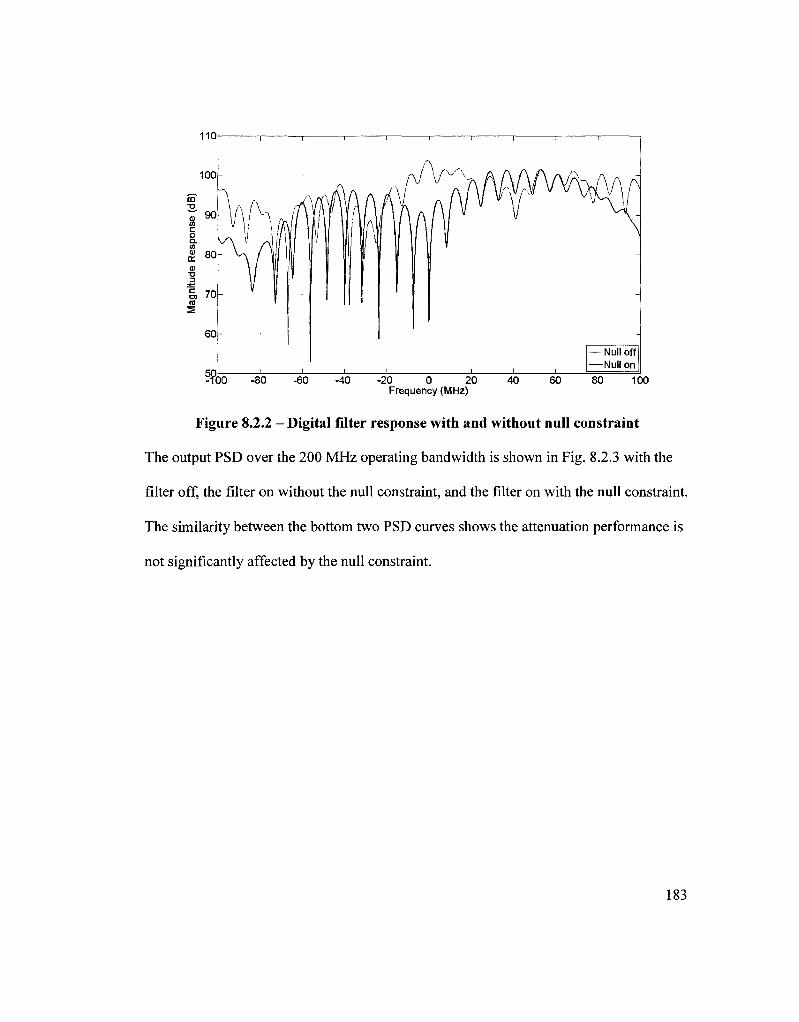
110
-20 0 20 Frequency (MHz)
100
Figure 8.2.2 - Digital filter response with and without null constraint
The output PSD over the 200 MHz operating bandwidth is shown in Fig. 8.2.3 with the
filter off, the filter on without the null constraint, and the filter on with the null constraint.
The similarity between the bottom two PSD curves shows the attenuation performance is
not significantly affected by the null constraint.
183

1000
N -100 •
E CD
Q -140 W
-161
1 1 1 1 1
" Filter On - Null Off
1 1 1 1 I
1 ! 1 1
W 820 840 860 880 900 920 940 960 980
-
V-v-
10
Figure 8.2.3 - Output PSD over operating bandwidth a) digital filter off b) filter on without null constraint c) filter on with null constraint
Multiple null constraints can be incorporated into the adaptive algorithm with the
technique described above. These constraints improve the noise performance. But, the
attenuation performance may degrade as the number of null constraints increase since
each constraint removes a degree of freedom from the adaptive FIR filter.
8.2.3 Digital IIR stage
The digital BSF compensation, denoted 'IIR stage', was shown to improve near band
attenuation in Section 7.2.3. The IIR stage was placed in the FPGA between the ADCl's
and the adaptive FIR filter input. The /?23, r[»] channel estimation algorithm would
produce more accurate near band results if the IIR stage were placed between the
adaptive FIR filter output and the DAC1 's. The hn\n\ channel would include this
compensation stage, thereby making the channel's magnitude response flatter outside the
184

passband. A flatter frequency response could contribute towards a more accurate channel
estimate, hence relaxing the stability criteria.
8.2.4 Negative Group Delay
Minimizing the group delay mismatch between the two FF paths was shown to improve
attenuation bandwidth performance. Adding group delay to the RF path is one technique
to minimize the group delay, but comes with the cost of a higher insertion loss in the RF
path. Alternatively, a negative group delay (NGD) circuit can be placed into the FF path
containing the digital components. This technique is applied to FF amplifier linearization
to reduce the excess delay in the main path by 40% in [47]. Narrowband NGD solutions
have been demonstrated in the literature at RF [48,49,50,51,52], analog baseband [53],
and digital baseband [54]. In fact, the converged frequency response of the digital filter in
the hybrid RF-DSP FF filter exhibits NGD at frequencies occupied by wideband input
signals. This NGD is demonstrated in Fig. 8.2.4 and 8.2.5, which shows the group delay
and magnitude responses from the hybrid RF-DSP FF filter's digital filter for a single
input with a 6 MHz bandwidth. The input signal is at 942.4 MHz, which is +42.4 MHz
relative to the filter's centre frequency of 900 MHz.
185

Q.
0
100
80
60
40
20
0
-20
-40
-60
-80
"10ft 00 -20 0 20 Frequency (MHz)
100
Figure 8.2.4 - Group delay response of single wideband input at +42.4 MHz
-20 0 20 Frequency (MHz)
100
Figure 8.2.5 - Magnitude response of single wideband input at +42.4 MHz
An NGD circuit would provide some of the negative group delay that the adaptive FIR
filter will be known to exhibit at frequencies occupied by wideband input signals.
186
Significant NGD is not attainable over the entire Nyquist bandwidth; so the NGD would
need to be tuned to the wideband input's frequency, which must be known a priori.
8.3 Discussion Summary
This chapter proposed some improvements for the hybrid RF-DSP FF filter, and made
some generalizations about the analysis. The proposed improvements and generalizations
are based on the analyses, simulations and measured results from the previous chapters.
8.4 Conclusion
Analyses, simulations and measurements have been reported for a new type of frequency
agile RF filter. Successful operation of the hardware prototype was demonstrated from
800 to 1800 MHz, and for filter orders between 32 and 64. The filter exhibits an all-zero
transfer function, which is best suited for providing multiple notches or stop-bands.
Wideband attenuation was also demonstrated, but required the addition of a delay line to
the RF FF path to attain nearly 25 dB attenuation over bandwidths as large as 8 MHz.
8.4.1 List of Contributions
The contributions made during this research are listed below:
1. A frequency agile RF feed-forward architecture with a digital filter in one of the
feed-forward paths with applications for frequency agile RF filtering and duplexer
isolation improvement.
187

2. Noise and attenuation analyses of this architecture that combines the effects of the
RF and digital systems. Also, first-order approximation expressions for dynamic
range and attenuation bandwidth performance.
3. Addition of an IIR stage within the digital filter to improve near-band attenuation
performance, and provide the means to reconfigure the passband bandwidth.
4. Addition of a negative group delay circuit in the feed-forward path containing the
digital filter to improve wideband attenuation performance.
5. Modification to active noise control adaptive algorithm for the hybrid RF-DSP FF
filter. The modification allows for a simpler relationship between the stability
criteria and the allowable estimation errors of the /223M channel.
6. Addition of notch constraints in the digital filter to reduce the output noise due to
the RF/Analog 1 chain and primary ADC's.
Two patent applications were filed by Nortel Networks with the Canadian Intellectual
Property Office based on the contributions. The author of this thesis is the single author
on both of these patent applications [5,6].
188
References
[1] S. Haykin, "Cognitive radio: brain-empowered wireless communications," IEEE Journal on Sel. Areas in Comms., vol. 23, no. 2, pp. 201-220, Feb. 2005.
[2] "Promoting more efficient use of spectrum through dynamic spectrum use technologies," FCC, Washington, D.C., Notice of inquiry FCC-10-198, 2010.
[3] T. Schilcher, "RF Applications in Digital Signal Processing," Digital Signal Processing CAS, p. 2490283, Jun. 2007.
[4] S. Elliott, Signal Processing for Active Control. San Diego, CA: Academic Press, 2001.
[5] Mark Wyville, Frequency agile filter using a digital filter and bandstop filtering, filing date: 26 Nov. 2009, publication date: 10 Jun. 2010, applic. no. PCT/CA2009/001721, WIPO publication no. WO2010/063096.
[6] Mark Wyville, Frequency agile filter using a digital filter and bandstop filtering, filing date: 26 Nov. 2009, pulication date: 10 Jun. 2010, applic. no. PCT/CA2009/001722, WIPO pulic. no. WO2010/063097.
[7] G. Fischer, "Next-generation base station radio frequency architecture," Bell Labs TechnicalJournal, vol. 12, no. 2, pp. 3-18, Dec. 2007.
[8] Herman J. Blinchikoff and Anatol I. Zverev, Filtering in the Time and Frequency Domains. New York, NY: Wiley, 1976, ch. 6.3.
[9] G. Rebeiz et al., "Tuning in to RF MEMS," IEEE Microwave Magazine, vol. 10, no. 6, pp. 55-72, Oct 2009.
[10] R.M. Young et al., "Low-loss bandpass RF filter using MEMS capacitance switches to acheive a one-octave tuning range and independently variable bandwidth," IEEE MTT-SInternational, vol. 3, pp. 1781-1784, Jun. 2003.
[11] H. Joshi, H.H. Sigmarsson, D. Peroulis, and W.J. Chappell, "Highly loaded evanescent cavities for widely tunable high-Q filters," IEEE MTT-S International, pp. 2133-2136, Jun. 2007.
[12] X. Liu, L.P.B. Katehi, W.J. Chappell, and D. Peroulis, "A 3.4-6.2 GHz continuously tunable electrostatic MEMS resonator with quality factor of 460-30," IEEE MTT-S International, pp. 1149-1152, Jun. 2009.
[13] S.-J. Park, I. Reines, C. Patel, and G.M. Rebeiz, "High Q RF-MEMS 4-6 GHz tunable evanescent-mode cavity filter," IEEE Transactions on MTT, vol. 58, no. 2, pp. 381-389, Feb. 2010.
[14] R. G. Meyer and M. L. Stephens, "Distortion in variable-capacitance diodes," IEEE Journal of Solid-State Circuits, vol. 10, no. 2, pp. 47-54, Feb. 1975.
[15] K. Buisman et al., "A monolithic low-distortion low-loss silicon-on-glass varactor-tuned filter with optimized biasing," IEEE Microwave and wireless components letters, vol. 17, no. 1, pp. 58-60, Jan. 2007.
[16] M. A. El-Tanani and G. M. Rebeiz, "A two-pole two-zero tunable filter with improved linearity," IEEE Trans, on MTT, vol. 57, no. 4, pp. 830-839, Apr. 2009.
[17] Skyworks, "Design with PIN Diodes (application note)," www.skyworksinc.com,
Apr. 2009. [18] H. Maune, M. Sazegar, Y. Zheng, A. Giere, and R. Jakoby, "Design of planar
varactors based on ferroelectric thick-films," German Microwave Conference, pp. 102-105, Mar. 2010.
[19] M.-T. Nguyen, W. D. Yan, and E. Home, "Broadband tunable filters using high Q passive tunable ICs," IEEE MTT-S International, pp. 951-954, Jun. 2008.
[20] G. Subramanyam et al., "Linearity and temperature dependence of large-area processed high-q barium strontium titanate thin-film varactors [Correspondence]," IEEE Trans. Ultrasonics, Ferroelectrics and Frequency Control, vol. 57, no. 7, pp. 1692-1695, Jul. 2010.
[21] T. Koryu Ishii, Ed., Handbook of Microwave Technology: Components and Devices. San Diego, CA: Academic Press, 1995.
[22] P.S. Carter Jr., "Magnetically-Tunable Microwave Filters Using Single-Crystal Yttrium-Iron-Garnet Resonators," IRE Trans, on MTT, vol. 9, no. 3, pp. 252-260, May 1961.
[23] J. K. Cavers, "Adaptation behaviour of a feedforward amplifier linearizer," IEEE
Trans, on Veh. Tech., vol. 44, no. 1, pp. 31-40, Feb. 1995.
[24] A. M. Smith and J. K. Cavers, "A wideband archtiecture for adaptive feedforward linearization," IEEE VTC, pp. 2488-2492, May 1998.
[25] R.G. Randall, J.G. McRory, and R.H. Johnston, "Broadband DSP based feedforward amplifier lineariser," Electronics Letters, vol. 38, no. 23, pp. 1470-1471, Nov. 2002.
[26] S. Ayazian and R. Gharpurey, "Feedforward Interference Cancellation in Radio Receiver Front-Ends," IEEE Trans, on Circuits and Systems II: Express Briefs, vol. 54, no. 10, pp. 901-906, Oct. 2007.
[27] T. O'Sullivan, R.A. York, B. Noren, and P.M. Asbeck, "Adaptive duplexer implemented using single-path and multipath feedforward techniques with BST phase shifters," IEEE Trans, on MTT, vol. 53, no. 1, pp. 106-114, Jan. 2005.
[28] A. Roussel, C.W. Nicholls, and J.S. Wight, "Frequency agile bandstop filter (FABSF)," IEEE MTT-S International, pp. 1099-1102, Jun. 2008.
[29] W. Schacherbauer, T. Ostertag, C.C.W. Ruppel, A. Springer, and R. Weigel, "An interference cancellation technique for the use in multiband software radio frontend design," 30th European Microwave Conference, pp. 1-4, Oct. 2000.
[30] S. Kannangara and M. Faulkner, "Adaptive duplexer for multiband transceiver," RAWCONProceeedings, pp. 381-384, Aug. 2003.
[31] S. Kannangara, "Adaptive Duplexer for Software Radio," Victoria University, Melbourne, AU, PhD dissertation 2006.
[32] Xiaopeng Li and Mohammed Ismail, Multi-Standard CMOS Wireless Receivers: Analysis and Design.: Springer, 2002.
[33] D. S. Chan and L. R. Rabiner, "Analysis of quantization error in the direct form for finite impulse response digital filters," IEEE Trans. Audio & Electroacoustics, vol. 21, no. 4, Aug. 1973.
[34] C. W. Barnes, B. N. Tran, and S. H. Leung, "On the statistics of fixed-point roundoff error," IEEE Trans. Acoustics, Speech, and Signal Processing, vol. 33, no. 3, pp.

191
595-606, Jun. 1985.
[35] J. G. Proakis and D. G. Manolakis, Digital Signal Processing Principles, Algorithms, and Applications, 3rd ed. New Jersey, NY: Prentice Hall, 1996.
[36] V-line directional coupler: 7.15S-dB-1.500V, Accessed 2011, e-MECA, avail: www.e-meca.com.
[37] V-line directional coupler: 722S-dB-1.500V, Accessed 2011, e-MECA, avail: www.e-meca.com.
[38] UMTS Base Station Radio Transmission and Reception (FDD), ETSI TS 125 104 v9.6.0 (2011-01), Accessed March 2011, 3GPP, avail: www.3gpp.org.
[39] AD9744 data sheet, Accessed 2010, Analog Devices, avail: www.analog.com.
[40] S. Haykin, Modern Filters. NY, NY: Macmillan Publishing Company, 1989. [41] S.L. Marple Jr., Digital Spectral Analysis with Applications. Englewood Cliffs, NJ:
Prentice-Hall Inc., 1987.
[42] S. Haykin, Adaptive Filter Theory, 4th ed. New Jersey, NY: Prentice Hall, 2002.
[43] S. M. Kuo and D. R. Morgan, "Active noise control: a tutorial review," Proceedings of the IEEE, vol. 87, no. 6, pp. 943-973, Jun 1999.
[44] G. A. Clark, S. K. Mitra, and S. R. Parker, "Block implementation of adaptive digital filters," IEEE Trans, on Acoustics, Speech, and Signal Processing, vol. 29, no. 3, pp. 744-752,Jun. 1981.
[45] ADS5474 data sheet, Accessed 2010, Texas Instruments, avail: www.ti.com.
[46] HMC630LP3 data sheet, Accessed 2010, Hittite Microwave, avail: www.hittite.com.
[47] H. Noto, K. Yamauchi, M. Nakayama, and Y. Isota, "Negative group delay circuit for feed-forward amplifier," IEEE MTT-S International, pp. 1103-1106, Jun. 2007.
[48] S.J. Erickson, H. Khaja, and M. Mojahedi, "Time- and frequency-domain measurements for an active negative group delay circuit," IEEE Antennas and Propagation Intern. Symp., vol. 3 A, pp. 790-793, Jul. 2005.
[49] B. Ravelo, A. Perennec, and M. Le Roy, "Synthesis of broadband negative group delay active circuits," IEEE MTT-S Intern., pp. 2177-2180, Jun. 2007.
[50] O.F. Siddiqui, M. Mojahedi, and G.V. Eleftheriades, "Periodically loaded transmission line with effective negative refractive index and negative group velocity," IEEE Trans. Antennas and Propagation, vol. 51, no. 10, pp. 2619-2625, Oct. 2003.
[51] CD. Broomfield and J.K.A. Everard, "Broadband negative group delay networks for compensation of microwave oscillators and filters," Electonics Letters, vol. 36, no. 23, pp. 1931-1933, Nov. 2000.
[52] S. Lucyszyn, I.D. Robertson, and A.H. Aghvami, "Negative group delay synthesiser," Electronic Letters, vol. 29, no. 9, pp. 798-800, Apr. 1993.
[53] B. Ravelo, A. Perennec, and M. Le Roy, "Equalization of interconnect propagation delay with negative group delay active circuits," IEEE Workshop on Signal Propagation on Interconnects, pp. 15-18, May 2007.
[54] U. Martin and H.W. Schussler, "On digital systems with negative group delay," Frequenz, vol. 47, no. 5-6, pp. 106-113, May-Jun. 1993.

192
[55] J. B. Knowles and E. M. Olcayto, "Coefficient accuracy and digital filter response," IEEE Trans. Circuit theory, vol. 15, no. 1, pp. 31-41, Mar. 1968.
[56] A. Papoulis and S. Unnikrishna Pillai, Probability, Random Variables and Stochastic Processes, 4th ed. NY, NY: McGraw-Hill, 2002.

193
Appendix A - Filter Tap Quantization
This appendix presents a statistical analysis relating the digital filter tap quantization to
the desired FF attenuation of the hybrid RF-DSP FF filter. The statistical analysis follows
that in [33], for a direct-form digital filter.
The frequency response of a discrete-time FIR filter with N infinite-precision taps is
given by:
HM^cMe-^ (A.1) n=0
In (A.l), co is the continuous-time frequency variable, and Tis the period of the digital
clock. The nth infinite-precision filter tap is denoted by Coo(n). A different frequency
response occurs when these taps are represented with finite-precision values, cjp(n).
Hjp{co) = fJcfp{nyin0'T (A.2)
The difference between the infinite and finite-precision frequency responses is:
H^) = HM-Hfp(co)=Nf[cx(n)-cfp(n)VJ"aT (A.3) «=o
The effect of the transfer function error is now translated into FF attenuation. Re
arranging (A.3) gives H fp (co) = Hm (co)- He(co). This relationship shows that the finite-
precision coefficient filter, Hfp(co), can be modeled by an infinite-precision filter,
Hx(co), in parallel with He(co) [55]. This parallel arrangement is shown in Fig. A.l.

51 H
C rcy Ln
H RF\ H 11 ADC
» ^*M — • ^ DAC H RF2 HBSF(a))
RF„
Q
/^.n //". rap
c, TTRF.
11 RF\ -¥ H 11 ADC
Hjfo) +
# » ** DAC -> H
11 RF2 HBSF(a))
out
Figure A.l - Mathematically equivalent models of hybrid FF filter with finite-
precision filter taps
In Fig. A.l, the transfer functions of the RF components are expressed in terms of their
baseband equivalent functions. All the component values are frequency dependent, but
the '(<*>)' term has only been appended to those components that intentionally exhibit a
frequency dependent magnitude response.
The bottom system in Fig. A.l consists of three parallel FF paths. If the infinite-precision
filter results in perfect FF cancellation at frequencies occupied by interferers (a>int), then
resulting magnitude response at these frequencies is:
\HFF fomt ) | = \He fomt ) | ' \HC\cH RF\H ADCH DACH RF2H BSF fomt )HC2c | (A.4)
The above derivation has followed that from [33], but the remainder of this derivation
does not. In [33], the goal was to determine the effect of coefficient quantization on the
mean square error ofHe(a>), integrated over all frequencies. In this derivation the goal is
to determine the effect of coefficient quantization on the magnitude of He((£>) only at

195
interferer frequencies. Furthermore, in [33] only real filter coefficients were considered,
but complex values are required for this analysis.
The error for each coefficient due to quantization is: ce(ri)=cx{n)-Cfp(ri). This definition
together with (A.3) yields (A.5). The coefficient error, ce(n), is decomposed into real and
imaginary parts.
N-l N-l
HM= Hce(n)e-^T = £ k ™ , ( " ) + j C v m v (n) ]*-""• (A.5) n=0 n=0
The strategy of this analysis is to perform a statistical analysis on He(co) in terms of the
tap quantization step-size, QTAPS- The transfer function errors of He(co) are related to the
attenuation of the hybrid RF-DSP FF filter, \HFF((O)\, hence can be related to QTAPS- This
step size is a function of the number of bits (bTAPs) used to represent the real and
imaginary components of the digital filter taps. The step-size also depends on the
maximum digital value used in the fixed-point representation (v^p^ .This value is the
maximum value for the real and imaginary components of the tap coefficient that can be
represented without saturation or wrap-around.
QTAPS = ~A„«-I (A > 6)
The real part and imaginary parts of He(co) are obtained using (A.5):
N-l
Re{HX(o)}=^cereal(n)cos(ncoT)+cemag{n)sin(n(i}T)
N-l
Im{He (©)} = £ - cejeal (n)sm{no)T) + cemag {n)cos(ncoT)
(A.7)
n=0
The coefficient quantization errors (ce) are assumed uniformly distributed from -QTAPS/2
to QTAPS/2- These components are independent in a direct-form filter since each
component is a unique input to the filter's multipliers. This independence means that
when m±n: E[cereai(m)ceireai(ri)]=0, and E[ce>imag(m)cejmag(n)]=0. Furthermore, for any m
and n, E[cereai{m)ceMag{ri)\=Q.
The mean and variance of each of the Af components in each of the summations in (A.7)
are equal. The mean and variance of the «th term in the Re{77e(co)} summation are
respectively:
E[ce,nai {n)cos(ncoT)+ce ,mag (n)sm(ncoT)] = 0
\ceUn)M™T)+ce,,mJn)sm(nc»T)\2] = ^ ^ <rl=E
Both the real and imaginary components of He(a>) are the sum of N independent
identically distributed random variables. For sufficiently large N, the central limit
theorem states the probability distribution of the real and imaginary components of He(co)
will converge to a Gaussian distribution [56]. Applying the central limit theorem means
that both Re{He(co)} and 1m{He(co)} have zero mean and variance Q*APSN/l2.
Equation (A.4) requires the magnitude of He(co). The magnitude of He(co) is a function of
the two Gaussian random variables in (A.7).
|//eM| = V[Re{^(«)}]2+[lm{//e(«)}]2 (A.9)
The probability distribution function of the magnitude of a complex Gaussian random
variable is the Rayleigh distribution [56]. The cumulative distribution function of the
Rayleigh distribution is:

197
Pr ( | #» |< / / J = l-exp f Hl^
2(TleJ 1 - exp
6H 2 \
V UTAPS^ J
(A.10)
This distribution function is illustrated in Fig. A.2. In this figure the y-axis is plotted on a
logarithmic axis to expand the relevant portion of the curve.
0 9997
0.977;
Figure A.2 - Rayleigh cumulative density function
From Fig. A.2 it can be seen that with probability of 0.9889, \He((o)\ will be upper
bounded by three standard deviations. The standard deviation is: aHe = QTAPS^N/\2 . The
probability that \He(co)\ is bounded by four standard deviations is 0.9997. Using four
standard deviations as the statistical upper bound:
\Ht(a)\Z4<rHe=2QTAPS<jj (AM)
The result in (A.l 1) can be used to choose QTAPS, based on N and the desired notch
degradation due to quantization. But, this limit on degradation is only valid 99.97% of the
time. The AaHe statistical upper bound from (A.l 1) is inserted into (A.4) to arrive at an
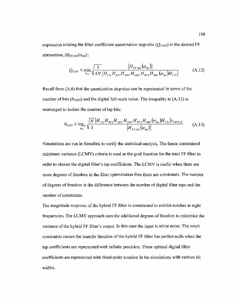
198
expression relating the filter coefficient quantization step-size (QTAPS) to the desired FF
attenuation, \HFFides((Hmt)\'
QTAPS<mmJ | ! ! -, r 1 (A.12) «v» \4N \HCXcHRFXHADCHDACHRF2HBSF[o)mt)HC2c\
Recall from (A.6) that the quantization step-size can be represented in terms of the
number of bits (bxAPs) and the digital full-scale value. The inequality in (A.12) is
rearranged to isolate the number of tap bits:
7 ^ 1 JN \"C\c"RF\"ADC**DAc"RF11*BSFV^mt)1*C2c\VTAPS,fi
bTAPS * log2 J - r - 7-^n (A. 13)
Simulations are run in Simulink to verify the statistical analysis. The linear constrained
minimum variance (LCMV) criteria is used as the goal function for the total FF filter in
order to choose the digital filter's tap coefficients. The LCMV is useful when there are
more degrees of freedom in the filter optimization then there are constraints. The number
of degrees of freedom is the difference between the number of digital filter taps and the
number of constraints.
The magnitude response of the hybrid FF filter is constrained to exhibit notches at eight
frequencies. The LCMV approach uses the additional degrees of freedom to minimize the
variance of the hybrid FF filter's output. In this case the input is white noise. The notch
constraints ensure the transfer function of the hybrid FF filter has perfect nulls when the
tap coefficients are represented with infinite precision. These optimal digital filter
coefficients are represented with fixed-point notation in the simulations with various bit
widths.

199
In the simulation, VTAPSJS-^, which is chosen empirically from the maximum values
required to obtain the desired notches in the transfer function. The cascaded magnitude
response of the RF and analog components is unity: \HCICHRFIHADCHDACHRF2HC2C\=^',
therefore \HFF{co)\=\He{(o)HBSF{(o)\. The latter relationship is used to extract \He(co)\ from
the simulation results. The number of digital filter taps is set to 32.
Repeated trials are required to validate a statistical analysis. In each trial eight frequency
notches are randomly assigned. This setup ensures the tap coefficients are not the same
values from trial to trial. The frequency response of the hybrid RF-DSP FF filter from
one trial is shown in Fig. A.3. The eight constrained notches are indicated with small
circles in Fig. A.3a at the -50 dB level. This figure is showing the magnitude response for
the maximum precision case.
10
0
m-10
8-20 c O £-30 <u
S-40 | - 5 0
1-60 -70 -81
:00 -150 -100 -50 0 Frequency (MHz)
-90
50 100 150 200 "1°?56
m
-20
-30
~ "40
d> V e n C -50 O Q .
| -60 <D
B -70
4° -80
- ^ ^ * J S S : = : : 5 ^ ; . z ^ ^ 5 3 5 * ^
•
, -
max 8 bit 10 bit 12 bit
— _ 14 bit
156 2 156 4 156 6 156 8 157 Frequency (MHz)
Figure A.3 a) Magnitude response of hybrid FF filter with maximum precision in the digital filter for a single trial b) Zoomed in magnitude response curves with
various tap coefficient bit widths
The simulation results in Fig. A.3b show the magnitude responses at one of the notch
locations for five different values of bjAPS- The degradation of notch depth is illustrated
for decreasing bit widths.
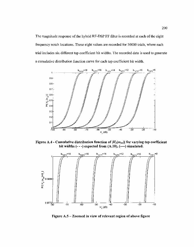
200
The magnitude response of the hybrid RF-DSP FF filter is recorded at each of the eight
frequency notch locations. These eight values are recorded for 50000 trials, where each
trial includes six different tap coefficient bit widths. The recorded data is used to generate
a cumulative distribution function curve for each tap coefficient bit width.
bTAPS=1 8 bTAPS=16 bTAPS=14 bTAPS=12 bTAPS=10 bTAPS=8
Figure A.4 - Cumulative distribution function of \He(o)int)\ for varying tap coefficient bit widths ( ) expected from (A.10), (—) simulated.
I V
£ 0 9889 -a>
I
0 977: %
b TAPS= 1 £
-70
b TAPS= 1 6
-60
bTAPS= 1 4 bTAPS=1 2 b TAPS= 1 0
-50 -40 H (dB)
-30 -20
bTAPS=8
I i i M I i
[, f , i i
f -10
Figure A.5 - Zoomed in view of relevant region of above figure
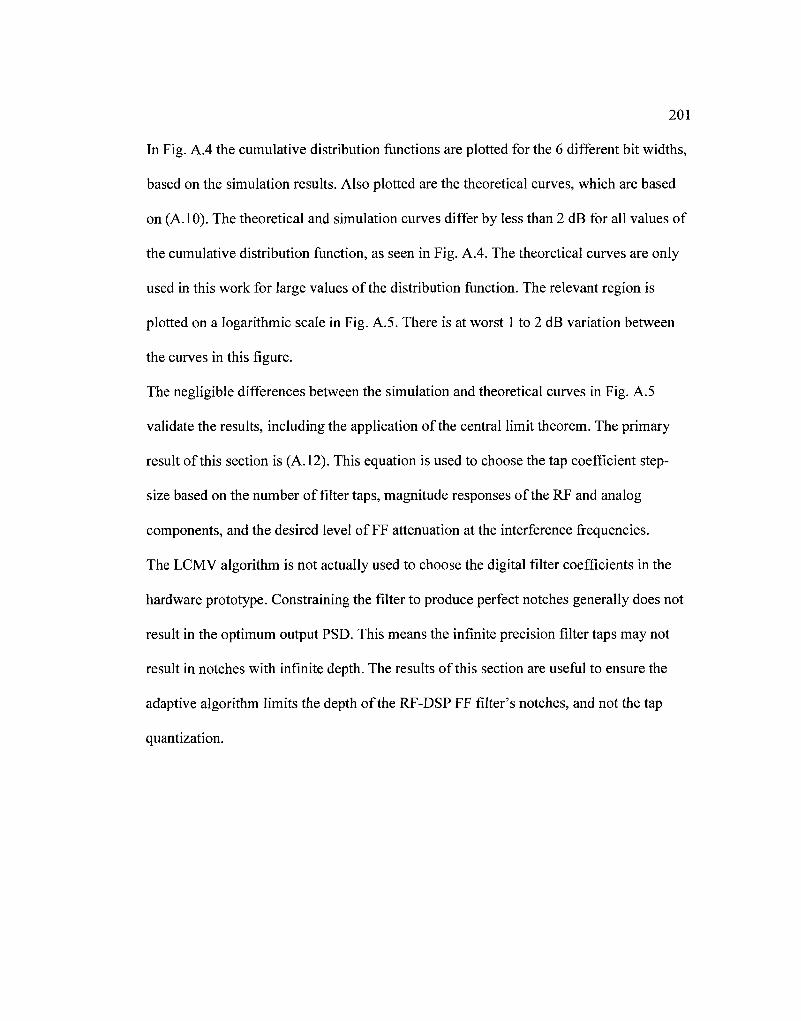
201
In Fig. A.4 the cumulative distribution functions are plotted for the 6 different bit widths,
based on the simulation results. Also plotted are the theoretical curves, which are based
on (A. 10). The theoretical and simulation curves differ by less than 2 dB for all values of
the cumulative distribution function, as seen in Fig. A.4. The theoretical curves are only
used in this work for large values of the distribution function. The relevant region is
plotted on a logarithmic scale in Fig. A.5. There is at worst 1 to 2 dB variation between
the curves in this figure.
The negligible differences between the simulation and theoretical curves in Fig. A.5
validate the results, including the application of the central limit theorem. The primary
result of this section is (A.12). This equation is used to choose the tap coefficient step-
size based on the number of filter taps, magnitude responses of the RF and analog
components, and the desired level of FF attenuation at the interference frequencies.
The LCMV algorithm is not actually used to choose the digital filter coefficients in the
hardware prototype. Constraining the filter to produce perfect notches generally does not
result in the optimum output PSD. This means the infinite precision filter taps may not
result in notches with infinite depth. The results of this section are useful to ensure the
adaptive algorithm limits the depth of the RF-DSP FF filter's notches, and not the tap
quantization.
Recommended