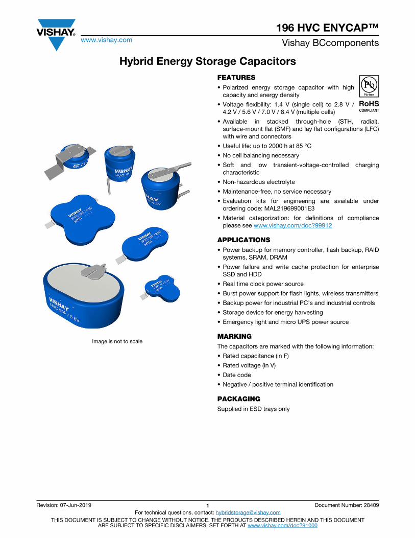
196 HVC ENYCAP™www.vishay.com Vishay BCcomponents
Revision: 07-Jun-2019 1 Document Number: 28409For technical questions, contact: [email protected]
THIS DOCUMENT IS SUBJECT TO CHANGE WITHOUT NOTICE. THE PRODUCTS DESCRIBED HEREIN AND THIS DOCUMENTARE SUBJECT TO SPECIFIC DISCLAIMERS, SET FORTH AT www.vishay.com/doc?91000
Hybrid Energy Storage Capacitors
Image is not to scale
FEATURES• Polarized energy storage capacitor with high
capacity and energy density
• Voltage flexibility: 1.4 V (single cell) to 2.8 V / 4.2 V / 5.6 V / 7.0 V / 8.4 V (multiple cells)
• Available in stacked through-hole (STH, radial), surface-mount flat (SMF) and lay flat configurations (LFC) with wire and connectors
• Useful life: up to 2000 h at 85 °C
• No cell balancing necessary
• Soft and low transient-voltage-controlled charging characteristic
• Non-hazardous electrolyte
• Maintenance-free, no service necessary
• Evaluation kits for engineering are available under ordering code: MAL219699001E3
• Material categorization: for definitions of compliance please see www.vishay.com/doc?99912
APPLICATIONS• Power backup for memory controller, flash backup, RAID
systems, SRAM, DRAM
• Power failure and write cache protection for enterprise SSD and HDD
• Real time clock power source
• Burst power support for flash lights, wireless transmitters
• Backup power for industrial PC’s and industrial controls
• Storage device for energy harvesting
• Emergency light and micro UPS power source
MARKINGThe capacitors are marked with the following information:
• Rated capacitance (in F)
• Rated voltage (in V)
• Date code
• Negative / positive terminal identification
PACKAGINGSupplied in ESD trays only
196 HVC ENYCAP™www.vishay.com Vishay BCcomponents
Revision: 07-Jun-2019 2 Document Number: 28409For technical questions, contact: [email protected]
THIS DOCUMENT IS SUBJECT TO CHANGE WITHOUT NOTICE. THE PRODUCTS DESCRIBED HEREIN AND THIS DOCUMENTARE SUBJECT TO SPECIFIC DISCLAIMERS, SET FORTH AT www.vishay.com/doc?91000
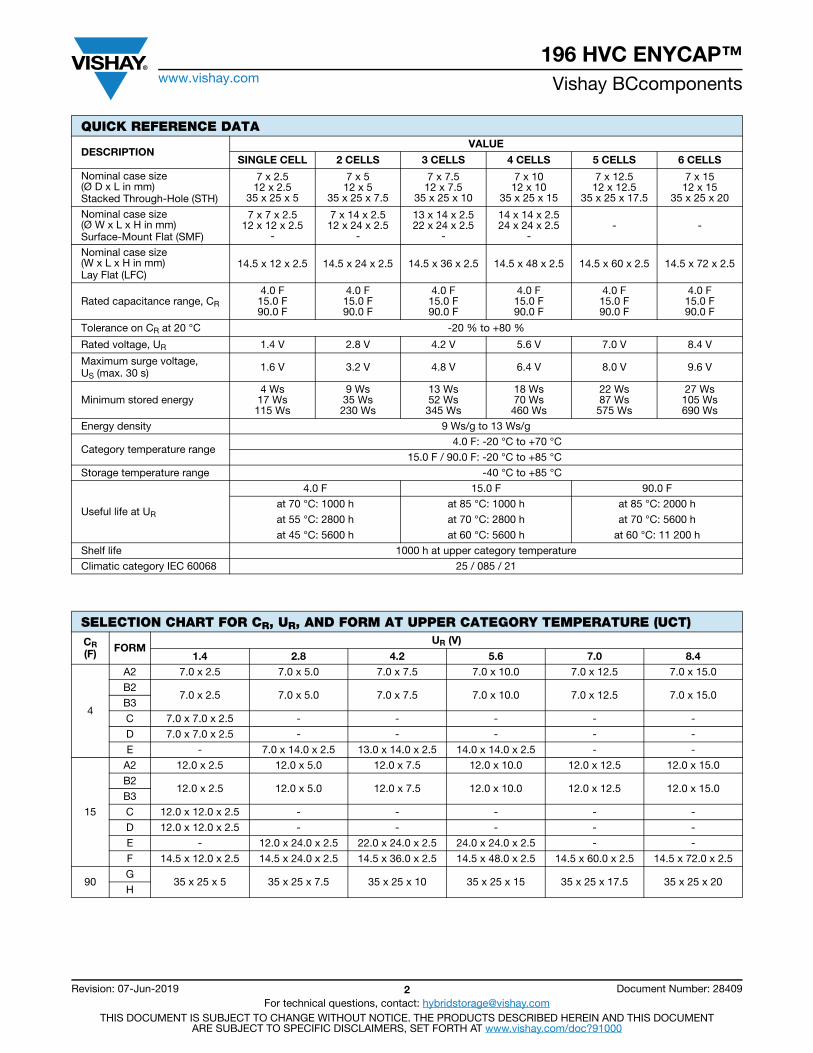
QUICK REFERENCE DATA
DESCRIPTIONVALUE
SINGLE CELL 2 CELLS 3 CELLS 4 CELLS 5 CELLS 6 CELLS
Nominal case size(Ø D x L in mm)Stacked Through-Hole (STH)
7 x 2.512 x 2.5
35 x 25 x 5
7 x 512 x 5
35 x 25 x 7.5
7 x 7.512 x 7.5
35 x 25 x 10
7 x 1012 x 10
35 x 25 x 15
7 x 12.512 x 12.5
35 x 25 x 17.5
7 x 1512 x 15
35 x 25 x 20
Nominal case size(Ø W x L x H in mm)Surface-Mount Flat (SMF)
7 x 7 x 2.512 x 12 x 2.5
-
7 x 14 x 2.512 x 24 x 2.5
-
13 x 14 x 2.522 x 24 x 2.5
-
14 x 14 x 2.524 x 24 x 2.5
-- -
Nominal case size(W x L x H in mm)Lay Flat (LFC)
14.5 x 12 x 2.5 14.5 x 24 x 2.5 14.5 x 36 x 2.5 14.5 x 48 x 2.5 14.5 x 60 x 2.5 14.5 x 72 x 2.5
Rated capacitance range, CR
4.0 F15.0 F90.0 F
4.0 F15.0 F90.0 F
4.0 F15.0 F90.0 F
4.0 F15.0 F90.0 F
4.0 F15.0 F90.0 F
4.0 F15.0 F90.0 F
Tolerance on CR at 20 °C -20 % to +80 %
Rated voltage, UR 1.4 V 2.8 V 4.2 V 5.6 V 7.0 V 8.4 V
Maximum surge voltage,US (max. 30 s) 1.6 V 3.2 V 4.8 V 6.4 V 8.0 V 9.6 V
Minimum stored energy4 Ws
17 Ws115 Ws
9 Ws35 Ws
230 Ws
13 Ws52 Ws
345 Ws
18 Ws70 Ws
460 Ws
22 Ws87 Ws
575 Ws
27 Ws105 Ws690 Ws
Energy density 9 Ws/g to 13 Ws/g
Category temperature range4.0 F: -20 °C to +70 °C
15.0 F / 90.0 F: -20 °C to +85 °C
Storage temperature range -40 °C to +85 °C
Useful life at UR
4.0 F 15.0 F 90.0 F
at 70 °C: 1000 h at 85 °C: 1000 h at 85 °C: 2000 h
at 55 °C: 2800 h at 70 °C: 2800 h at 70 °C: 5600 h
at 45 °C: 5600 h at 60 °C: 5600 h at 60 °C: 11 200 h
Shelf life 1000 h at upper category temperature
Climatic category IEC 60068 25 / 085 / 21
SELECTION CHART FOR CR, UR, AND FORM AT UPPER CATEGORY TEMPERATURE (UCT)CR(F) FORM
UR (V)
1.4 2.8 4.2 5.6 7.0 8.4
4
A2 7.0 x 2.5 7.0 x 5.0 7.0 x 7.5 7.0 x 10.0 7.0 x 12.5 7.0 x 15.0
B27.0 x 2.5 7.0 x 5.0 7.0 x 7.5 7.0 x 10.0 7.0 x 12.5 7.0 x 15.0
B3
C 7.0 x 7.0 x 2.5 - - - - -
D 7.0 x 7.0 x 2.5 - - - - -
E - 7.0 x 14.0 x 2.5 13.0 x 14.0 x 2.5 14.0 x 14.0 x 2.5 - -
15
A2 12.0 x 2.5 12.0 x 5.0 12.0 x 7.5 12.0 x 10.0 12.0 x 12.5 12.0 x 15.0
B212.0 x 2.5 12.0 x 5.0 12.0 x 7.5 12.0 x 10.0 12.0 x 12.5 12.0 x 15.0
B3
C 12.0 x 12.0 x 2.5 - - - - -
D 12.0 x 12.0 x 2.5 - - - - -
E - 12.0 x 24.0 x 2.5 22.0 x 24.0 x 2.5 24.0 x 24.0 x 2.5 - -
F 14.5 x 12.0 x 2.5 14.5 x 24.0 x 2.5 14.5 x 36.0 x 2.5 14.5 x 48.0 x 2.5 14.5 x 60.0 x 2.5 14.5 x 72.0 x 2.5
90G
35 x 25 x 5 35 x 25 x 7.5 35 x 25 x 10 35 x 25 x 15 35 x 25 x 17.5 35 x 25 x 20H
196 HVC ENYCAP™www.vishay.com Vishay BCcomponents
Revision: 07-Jun-2019 3 Document Number: 28409For technical questions, contact: [email protected]
THIS DOCUMENT IS SUBJECT TO CHANGE WITHOUT NOTICE. THE PRODUCTS DESCRIBED HEREIN AND THIS DOCUMENTARE SUBJECT TO SPECIFIC DISCLAIMERS, SET FORTH AT www.vishay.com/doc?91000
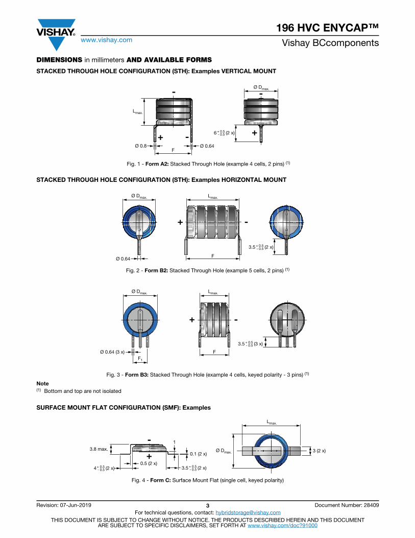
DIMENSIONS in millimeters AND AVAILABLE FORMS
STACKED THROUGH HOLE CONFIGURATION (STH): Examples VERTICAL MOUNT
Fig. 1 - Form A2: Stacked Through Hole (example 4 cells, 2 pins) (1)
STACKED THROUGH HOLE CONFIGURATION (STH): Examples HORIZONTAL MOUNT
Fig. 2 - Form B2: Stacked Through Hole (example 5 cells, 2 pins) (1)
Fig. 3 - Form B3: Stacked Through Hole (example 4 cells, keyed polarity - 3 pins) (1)
Note(1) Bottom and top are not isolated
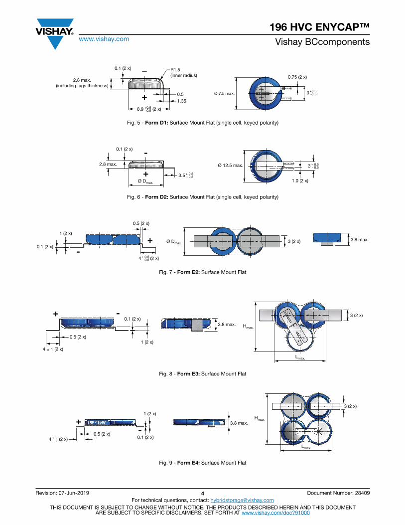
SURFACE MOUNT FLAT CONFIGURATION (SMF): Examples
Fig. 4 - Form C: Surface Mount Flat (single cell, keyed polarity)
Lmax.
Ø Dmax.
F
+ +
- -
-Ø 0.8 Ø 0.64
6 (2 x)+ 0.5- 0.5
Lmax.Ø Dmax.
F
+ -
Ø 0.64
3.5 (2 x)+ 0.5- 0.5
Lmax.
FØ 0.64 (3 x)F1
+ -
Ø Dmax.
3.5 (3 x)+ 0.5- 0.5
3 (2 x)0.1 (2 x)
0.5 (2 x)
3.8 max.
1
3.5 (2 x)+ 0.5- 0.54 (2 x)+ 0.5
- 0.5
Lmax.
Ø Dmax.+
-
196 HVC ENYCAP™www.vishay.com Vishay BCcomponents
Revision: 07-Jun-2019 4 Document Number: 28409For technical questions, contact: [email protected]
THIS DOCUMENT IS SUBJECT TO CHANGE WITHOUT NOTICE. THE PRODUCTS DESCRIBED HEREIN AND THIS DOCUMENTARE SUBJECT TO SPECIFIC DISCLAIMERS, SET FORTH AT www.vishay.com/doc?91000
Fig. 5 - Form D1: Surface Mount Flat (single cell, keyed polarity)
Fig. 6 - Form D2: Surface Mount Flat (single cell, keyed polarity)
Fig. 7 - Form E2: Surface Mount Flat
Fig. 8 - Form E3: Surface Mount Flat
Fig. 9 - Form E4: Surface Mount Flat
3+0.5-0.5Ø 7.5 max.
0.75 (2 x)0
+
_0.1 (2 x)
2.8 max.(including tags thickness)
R1.5(inner radius)
0.51.35
8.9 (2 x)+0.5-0.5
3 + 0.5- 0.5
3.5 + 0.2- 0.2
Ø 12.5 max.
0.1 (2 x)
2.8 max.
1.0 (2 x)+
-
Ø Dmax.
3 (2 x)Ø Dmax.3.8 max.+
-
0.5 (2 x)
1 (2 x)
0.1 (2 x)
4 (2 x)+ 0.5- 0.5
Hmax.
Lmax.
3 (2 x)+ -0.1 (2 x)
4 ± 1 (2 x)
0.5 (2 x)1 (2 x)
3.8 max.
Hmax.3.8 max.
0.5 (2 x)0.1 (2 x)
1 (2 x)
Lmax.
3 (2 x)
4 (2 x)+ 1- 1
+-
196 HVC ENYCAP™www.vishay.com Vishay BCcomponents
Revision: 07-Jun-2019 5 Document Number: 28409For technical questions, contact: [email protected]
THIS DOCUMENT IS SUBJECT TO CHANGE WITHOUT NOTICE. THE PRODUCTS DESCRIBED HEREIN AND THIS DOCUMENTARE SUBJECT TO SPECIFIC DISCLAIMERS, SET FORTH AT www.vishay.com/doc?91000
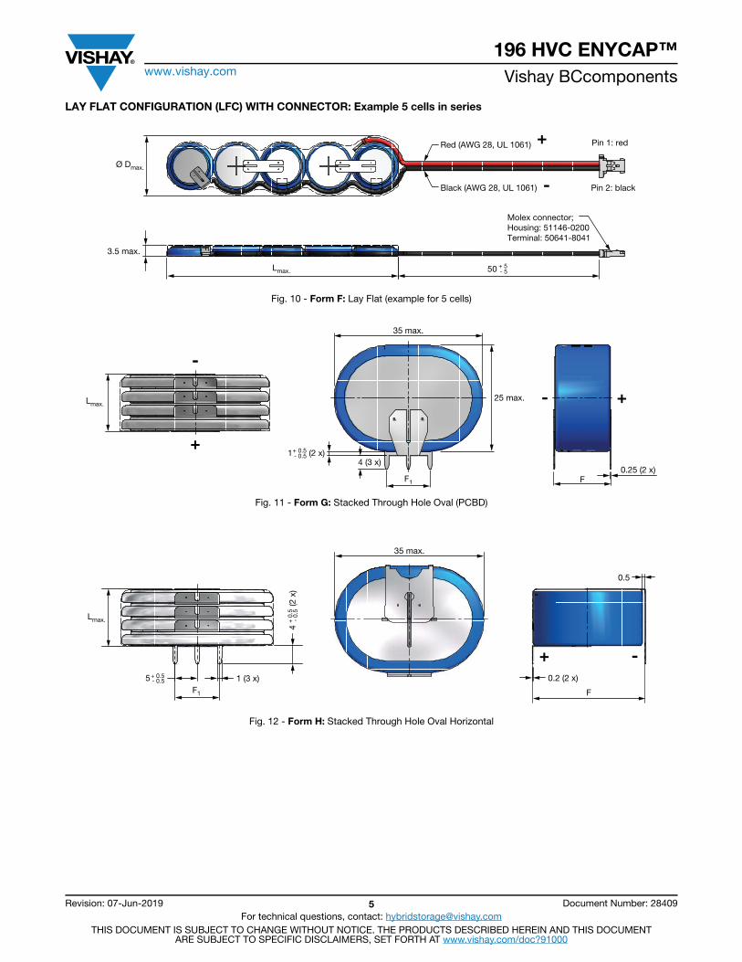
LAY FLAT CONFIGURATION (LFC) WITH CONNECTOR: Example 5 cells in series
Fig. 10 - Form F: Lay Flat (example for 5 cells)
Fig. 11 - Form G: Stacked Through Hole Oval (PCBD)
Fig. 12 - Form H: Stacked Through Hole Oval Horizontal
Red (AWG 28, UL 1061)
Black (AWG 28, UL 1061)
Molex connector;Housing: 51146-0200Terminal: 50641-8041
Lmax.
3.5 max.
Ø Dmax.
Pin 1: red
Pin 2: black
+
-
50 + 5- 5
+-
+
-
Lmax.
4 (3 x)
F1
1 (2 x)+ 0.5- 0.5
35 max.
25 max.
F0.25 (2 x)
Lmax.
F1
5
35 max.
1 (3 x)
4
(2
x)
+ 0
.5-
0.5
0.2 (2 x)
F
0.5
+ -+ 0.5- 0.5
196 HVC ENYCAP™www.vishay.com Vishay BCcomponents
Revision: 07-Jun-2019 6 Document Number: 28409For technical questions, contact: [email protected]
THIS DOCUMENT IS SUBJECT TO CHANGE WITHOUT NOTICE. THE PRODUCTS DESCRIBED HEREIN AND THIS DOCUMENTARE SUBJECT TO SPECIFIC DISCLAIMERS, SET FORTH AT www.vishay.com/doc?91000
Table 1
DIMENSIONS in millimeters, MASS AND PACKAGING QUANTITIESNOMINAL CASE SIZE
D x L x H (mm) FORM Ø Dmax. Lmax. L1max. Hmax.MASS
(g)
7.0 x 7.0 x 2.5 A2, B2, B3 7.5 2.3 + 0.3 7.0 + 0.5 - 0.5
7.0 x 7.0 x 2.5 C 7.5 7.0 7.0 + 8.0 - 0.5
7.0 x 7.0 x 2.5 D1 7.5 7.0 7.0 + 4.0 - 0.5
7.0 x 7.0 x 5.0 A2, B2, B3 7.5 4.2 4.2 + 0.5 - 0.8
7.0 x 7.0 x 7.5 A2, B2, B3 7.5 7.5 7.8 + 0.5 - 1.5
7.0 x 7.0 x 10.0 A2, B2, B3 7.5 10.5 10.2 + 0.5 - 1.8
7.0 x 7.0 x 12.5 A2, B2, B3 7.5 12.5 12.4 + 0.5 - 2.5
7.0 x 7.0 x 15.0 A2, B2, B3 7.5 14.8 14.8 + 0.5 - 3.0
12.0 x 12.0 x 2.5 A2, B2, B3 12.5 2.3 2.3 + 0.5 - 1.2
12.0 x 12.0 x 2.5 C 12.5 12.5 12.5 + 8.0 - 1.0
12.0 x 12.0 x 2.5 D2 12.5 12.5 12.5 + 4.0 - 1.0
12.0 x 12.0 x 5.0 A2, B2, B3 12.5 4.2 4.2 + 0.5 - 2.2
12.0 x 12.0 x 7.5 A2, B2, B3 12.5 8.0 7.8 + 0.5 - 3.3
12.0 x 12.0 x 10.0 A2, B2, B3 12.5 10.5 10.5 + 0.5 - 4.0
12.0 x 12.0 x 12.5 A2, B2, B3 12.5 12.5 12.5 + 0.5 - 5.4
12.0 x 12.0 x 15.0 A2, B2, B3 12.5 14.8 14.8 + 0.5 - 6.5
7.0 x 14.0 x 2.5 E2 7.5 14.8 14.8 + 8.0 - 1.0
12.0 x 24.0 x 2.5 E2 12.5 24.0 24.0 + 8.0 - 2.0
13.0 x 14.0 x 2.5 E3 14.0 15.0 14.8 + 8.0 14.0 1.2
22.0 x 24.0 x 2.5 E3 24.0 24.0 24.8 + 8.0 15.0 3.3
14.0 x 14.0 x 2.5 E4 15.0 15.0 14.8 + 8.0 22.5 1.5
24.0 x 24.0 x 2.5 E4 24.0 24.0 24.8 + 8.0 24.0 4.4
14.5 x 12.0 x 2.5 F 14.5 12.0 12.0 + 50.0 - 1.0
14.5 x 24.0 x 2.5 F 14.5 24.0 24.0 + 50.0 - 3.0
14.5 x 36.0 x 2.5 F 14.5 36.0 36.0 + 50.0 - 4.0
14.5 x 48.0 x 2.5 F 14.5 48.0 48.0 + 50.0 - 6.0
14.5 x 60.0 x 2.5 F 14.5 60.0 60.0 + 50.0 - 7.5
14.5 x 72.0 x 2.5 F 14.5 72.0 72.0 + 50.0 - 9.0
35 x 25 x 5.0 G, H 35 x 25 3.7 3.6 ± 0.1 - 7.5
35 x 25 x 7.5 G, H 35 x 25 7.5 7.5 + 0.5 - 15.0
35 x 25 x 10.0 G, H 35 x 25 10.5 10.5 + 0.5 - 22.5
35 x 25 x 15.0 G, H 35 x 25 15.0 14.5 + 0.5 - 30.0
35 x 25 x 17.5 G, H 35 x 25 17.8 16.8 ± 1.0 - 45.0
35 x 25 x 20.0 G, H 35 x 25 21.1 20.1 ± 1.0 - 50.0
196 HVC ENYCAP™www.vishay.com Vishay BCcomponents
Revision: 07-Jun-2019 7 Document Number: 28409For technical questions, contact: [email protected]
THIS DOCUMENT IS SUBJECT TO CHANGE WITHOUT NOTICE. THE PRODUCTS DESCRIBED HEREIN AND THIS DOCUMENTARE SUBJECT TO SPECIFIC DISCLAIMERS, SET FORTH AT www.vishay.com/doc?91000
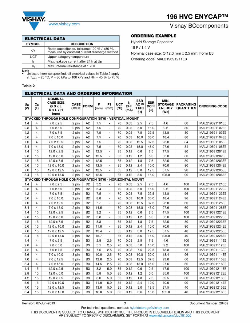
Note• Unless otherwise specified, all electrical values in Table 2 apply
at Tamb = 20 °C, P = 86 kPa to 106 kPa and RH = 45 % to 75 %
ORDERING EXAMPLEHybrid Storage Capacitor
15 F / 1.4 V
Nominal case size: Ø 12.0 mm x 2.5 mm; Form B3
Ordering code: MAL219691211E3
Table 2
ELECTRICAL DATASYMBOL DESCRIPTION
CRRated capacitance, tolerance -20 % / +80 %, measured by constant current discharge method
UCT Upper category temperatureIL Max. leakage current after 24 h at UR
RI Max. internal resistance at 1 kHz
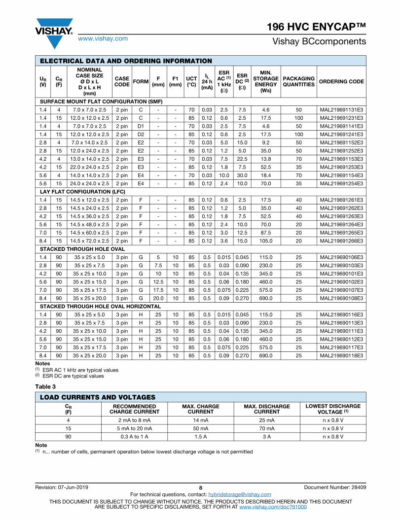
ELECTRICAL DATA AND ORDERING INFORMATION
UR(V)
CR(F)
NOMINALCASE SIZE
Ø D x LD x L x H
(mm)
CASECODE FORM F
(mm)F1
(mm)UCT(°C)
IL24 h(mA)
ESRAC (1)
1 kHz()
ESRDC (2)
()
MIN.STORAGEENERGY
(Ws)
PACKAGINGQUANTITIES ORDERING CODE
STACKED THROUGH HOLE CONFIGURATION (STH) - VERTICAL MOUNT1.4 4 7.0 x 2.5 2 pin A2 7.5 - 70 0.03 2.5 7.5 4.6 80 MAL219691101E3 2.8 4 7.0 x 5.0 2 pin A2 7.5 - 70 0.03 5.0 15.0 9.2 80 MAL219691102E3 4.2 4 7.0 x 7.5 2 pin A2 7.5 - 70 0.03 7.5 22.5 13.8 80 MAL219691103E3 5.6 4 7.0 x 10.0 2 pin A2 7.5 - 70 0.03 10.0 30.0 18.4 80 MAL219691104E3 7.0 4 7.0 x 12.5 2 pin A2 7.5 - 70 0.03 12.5 37.5 23.0 84 MAL219691105E3 8.4 4 7.0 x 15.0 2 pin A2 7.5 - 70 0.03 15.0 45.0 27.6 84 MAL219691106E3 1.4 15 12.0 x 2.5 2 pin A2 12.5 - 85 0.12 0.6 2.5 17.5 80 MAL219691201E3 2.8 15 12.0 x 5.0 2 pin A2 12.5 - 85 0.12 1.2 5.0 35.0 80 MAL219691202E3 4.2 15 12.0 x 7.5 2 pin A2 12.5 - 85 0.12 1.8 7.5 52.5 80 MAL219691203E3 5.6 15 12.0 x 10.0 2 pin A2 12.5 - 85 0.12 2.4 10.0 70.0 80 MAL219691204E3 7.0 15 12.0 x 12.5 2 pin A2 12.5 - 85 0.12 3.0 12.5 87.5 90 MAL219691205E3 8.4 15 12.0 x 15.0 2 pin A2 12.5 - 85 0.12 3.6 15.0 105.0 90 MAL219691206E3 STACKED THROUGH HOLE CONFIGURATION (STH) - HORIZONTAL MOUNT1.4 4 7.0 x 2.5 2 pin B2 3.2 - 70 0.03 2.5 7.5 4.6 100 MAL219691121E3 2.8 4 7.0 x 5.0 2 pin B2 5.4 - 70 0.03 5.0 15.0 9.2 100 MAL219691122E3 4.2 4 7.0 x 7.5 2 pin B2 7.5 - 70 0.03 7.5 22.5 13.8 96 MAL219691123E3 5.6 4 7.0 x 10.0 2 pin B2 8.8 - 70 0.03 10.0 30.0 18.4 96 MAL219691124E3 7.0 4 7.0 x 12.5 2 pin B2 12 - 70 0.03 12.5 37.5 23.0 60 MAL219691125E3 8.4 4 7.0 x 15.0 2 pin B2 14.5 - 70 0.03 15.0 45.0 27.6 60 MAL219691126E3 1.4 15 12.0 x 2.5 2 pin B2 3.2 - 85 0.12 0.6 2.5 17.5 100 MAL219691221E3 2.8 15 12.0 x 5.0 2 pin B2 5.8 - 85 0.12 1.2 5.0 35.0 100 MAL219691222E3 4.2 15 12.0 x 7.5 2 pin B2 8.3 - 85 0.12 1.8 7.5 52.5 80 MAL219691223E3 5.6 15 12.0 x 10.0 2 pin B2 11.0 - 85 0.12 2.4 10.0 70.0 90 MAL219691224E3 7.0 15 12.0 x 12.5 2 pin B2 13.4 - 85 0.12 3.0 12.5 87.5 40 MAL219691225E3 8.4 15 12.0 x 15.0 2 pin B2 15.7 - 85 0.12 3.6 15.0 105.0 40 MAL219691226E3 1.4 4 7.0 x 2.5 3 pin B3 2.8 2.5 70 0.03 2.5 7.5 4.6 100 MAL219691111E3 2.8 4 7.0 x 5.0 3 pin B3 5.1 2.5 70 0.03 5.0 15.0 9.2 100 MAL219691112E3 4.2 4 7.0 x 7.5 3 pin B3 7.5 2.5 70 0.03 7.5 22.5 13.8 96 MAL219691113E3 5.6 4 7.0 x 10.0 3 pin B3 10.0 2.5 70 0.03 10.0 30.0 18.4 96 MAL219691114E3 7.0 4 7.0 x 12.5 3 pin B3 12.0 2.5 70 0.03 12.5 37.5 23.0 60 MAL219691115E3 8.4 4 7.0 x 15.0 3 pin B3 14.5 2.5 70 0.03 15.0 45.0 27.6 60 MAL219691116E3 1.4 15 12.0 x 2.5 3 pin B3 3.2 5.0 85 0.12 0.6 2.5 17.5 100 MAL219691211E3 2.8 15 12.0 x 5.0 3 pin B3 5.8 5.0 85 0.12 1.2 5.0 35.0 100 MAL219691212E3 4.2 15 12.0 x 7.5 3 pin B3 8.0 5.0 85 0.12 1.8 7.5 52.5 80 MAL219691213E3 5.6 15 12.0 x 10.0 3 pin B3 11.0 5.0 85 0.12 2.4 10.0 70.0 90 MAL219691214E3 7.0 15 12.0 x 12.5 3 pin B3 13.0 5.0 85 0.12 3.0 12.5 87.5 40 MAL219691215E3 8.4 15 12.0 x 15.0 3 pin B3 16.0 5.0 85 0.12 3.6 15.0 105.0 40 MAL219691216E3
196 HVC ENYCAP™www.vishay.com Vishay BCcomponents
Revision: 07-Jun-2019 8 Document Number: 28409For technical questions, contact: [email protected]
THIS DOCUMENT IS SUBJECT TO CHANGE WITHOUT NOTICE. THE PRODUCTS DESCRIBED HEREIN AND THIS DOCUMENTARE SUBJECT TO SPECIFIC DISCLAIMERS, SET FORTH AT www.vishay.com/doc?91000
Notes(1) ESR AC 1 kHz are typical values(2) ESR DC are typical values
Table 3
Note(1) n... number of cells, permanent operation below lowest discharge voltage is not permitted
SURFACE MOUNT FLAT CONFIGURATION (SMF)
1.4 4 7.0 x 7.0 x 2.5 2 pin C - - 70 0.03 2.5 7.5 4.6 50 MAL219691131E3
1.4 15 12.0 x 12.0 x 2.5 2 pin C - - 85 0.12 0.6 2.5 17.5 100 MAL219691231E3
1.4 4 7.0 x 7.0 x 2.5 2 pin D1 - - 70 0.03 2.5 7.5 4.6 50 MAL219691141E3
1.4 15 12.0 x 12.0 x 2.5 2 pin D2 - - 85 0.12 0.6 2.5 17.5 100 MAL219691241E3
2.8 4 7.0 x 14.0 x 2.5 2 pin E2 - - 70 0.03 5.0 15.0 9.2 50 MAL219691152E3
2.8 15 12.0 x 24.0 x 2.5 2 pin E2 - - 85 0.12 1.2 5.0 35.0 50 MAL219691252E3
4.2 4 13.0 x 14.0 x 2.5 2 pin E3 - - 70 0.03 7.5 22.5 13.8 70 MAL219691153E3
4.2 15 22.0 x 24.0 x 2.5 2 pin E3 - - 85 0.12 1.8 7.5 52.5 35 MAL219691253E3
5.6 4 14.0 x 14.0 x 2.5 2 pin E4 - - 70 0.03 10.0 30.0 18.4 70 MAL219691154E3
5.6 15 24.0 x 24.0 x 2.5 2 pin E4 - - 85 0.12 2.4 10.0 70.0 35 MAL219691254E3
LAY FLAT CONFIGURATION (LFC)
1.4 15 14.5 x 12.0 x 2.5 2 pin F - - 85 0.12 0.6 2.5 17.5 40 MAL219691261E3
2.8 15 14.5 x 24.0 x 2.5 2 pin F - - 85 0.12 1.2 5.0 35.0 40 MAL219691262E3
4.2 15 14.5 x 36.0 x 2.5 2 pin F - - 85 0.12 1.8 7.5 52.5 40 MAL219691263E3
5.6 15 14.5 x 48.0 x 2.5 2 pin F - - 85 0.12 2.4 10.0 70.0 20 MAL219691264E3
7.0 15 14.5 x 60.0 x 2.5 2 pin F - - 85 0.12 3.0 12.5 87.5 20 MAL219691265E3
8.4 15 14.5 x 72.0 x 2.5 2 pin F - - 85 0.12 3.6 15.0 105.0 20 MAL219691266E3
STACKED THROUGH HOLE OVAL
1.4 90 35 x 25 x 5.0 3 pin G 5 10 85 0.5 0.015 0.045 115.0 25 MAL219690106E3
2.8 90 35 x 25 x 7.5 3 pin G 7.5 10 85 0.5 0.03 0.090 230.0 25 MAL219690103E3
4.2 90 35 x 25 x 10.0 3 pin G 10 10 85 0.5 0.04 0.135 345.0 25 MAL219690101E3
5.6 90 35 x 25 x 15.0 3 pin G 12.5 10 85 0.5 0.06 0.180 460.0 25 MAL219690102E3
7.0 90 35 x 25 x 17.5 3 pin G 17.5 10 85 0.5 0.075 0.225 575.0 25 MAL219690107E3
8.4 90 35 x 25 x 20.0 3 pin G 20.0 10 85 0.5 0.09 0.270 690.0 25 MAL219690108E3
STACKED THROUGH HOLE OVAL HORIZONTAL
1.4 90 35 x 25 x 5.0 3 pin H 25 10 85 0.5 0.015 0.045 115.0 25 MAL219690116E3
2.8 90 35 x 25 x 7.5 3 pin H 25 10 85 0.5 0.03 0.090 230.0 25 MAL219690113E3
4.2 90 35 x 25 x 10.0 3 pin H 25 10 85 0.5 0.04 0.135 345.0 25 MAL219690111E3
5.6 90 35 x 25 x 15.0 3 pin H 25 10 85 0.5 0.06 0.180 460.0 25 MAL219690112E3
7.0 90 35 x 25 x 17.5 3 pin H 25 10 85 0.5 0.075 0.225 575.0 25 MAL219690117E3
8.4 90 35 x 25 x 20.0 3 pin H 25 10 85 0.5 0.09 0.270 690.0 25 MAL219690118E3
LOAD CURRENTS AND VOLTAGESCR(F)
RECOMMENDED CHARGE CURRENT
MAX. CHARGECURRENT
MAX. DISCHARGECURRENT
LOWEST DISCHARGE VOLTAGE (1)
4 2 mA to 8 mA 14 mA 25 mA n x 0.8 V
15 5 mA to 20 mA 50 mA 70 mA n x 0.8 V
90 0.3 A to 1 A 1.5 A 3 A n x 0.8 V
ELECTRICAL DATA AND ORDERING INFORMATION
UR(V)
CR(F)
NOMINALCASE SIZE
Ø D x LD x L x H
(mm)
CASECODE FORM F
(mm)F1
(mm)UCT(°C)
IL24 h(mA)
ESRAC (1)
1 kHz()
ESRDC (2)
()
MIN.STORAGEENERGY
(Ws)
PACKAGINGQUANTITIES ORDERING CODE
196 HVC ENYCAP™www.vishay.com Vishay BCcomponents
Revision: 07-Jun-2019 9 Document Number: 28409For technical questions, contact: [email protected]
THIS DOCUMENT IS SUBJECT TO CHANGE WITHOUT NOTICE. THE PRODUCTS DESCRIBED HEREIN AND THIS DOCUMENTARE SUBJECT TO SPECIFIC DISCLAIMERS, SET FORTH AT www.vishay.com/doc?91000
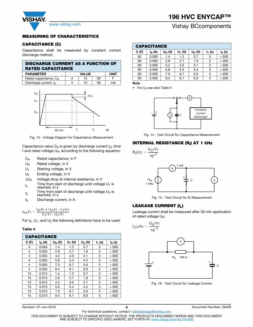
MEASURING OF CHARACTERISTICS
CAPACITANCE (C)Capacitance shall be measured by constant current discharge method.
Fig. 13 - Voltage Diagram for Capacitance Measurement
Capacitance value CR is given by discharge current ID, time t and rated voltage UR, according to the following equation:
For ID, U1, and U2 the following definitions have to be used:
Table 4
Note• For U2 see also Table 5
Fig. 14 - Test Circuit for Capacitance Measurement
INTERNAL RESISTANCE (RI) AT 1 kHz
Fig. 15 - Test Circuit for RI Measurement
LEAKAGE CURRENT (IL)Leakage current shall be measured after 30 min application of rated voltage UR:
Fig. 16 - Test Circuit for Leakage Current
DISCHARGE CURRENT AS A FUNCTION OFRATED CAPACITANCEPARAMETER VALUE UNITRated capacitance, CR 4 15 90 FDischarge current, ID 4 15 90 mA
CR Rated capacitance, in FUR Rated voltage, in VU1 Starting voltage, in VU2 Ending voltage, in VU3 Voltage drop at internal resistance, in V
t1Time from start of discharge until voltage U1 is reached, in s
t2Time from start of discharge until voltage U2 is reached, in s
ID Discharge current, in A
CAPACITANCEC (F) ID (A) UR (V) U1 (V) U2 (V) t1 (s) t2 (s)
4 0.004 1.4 1.3 0.7 5 > 6004 0.004 2.8 2.7 1.9 5 > 6004 0.004 4.2 4.0 3.1 5 > 6004 0.004 5.6 5.4 4.4 5 > 6004 0.004 7.0 6.7 5.6 5 > 6004 0.004 8.4 8.1 6.9 5 > 600
15 0.015 1.4 1.3 0.7 5 > 60015 0.015 2.8 2.7 1.9 5 > 60015 0.015 4.2 4.0 3.1 5 > 60015 0.015 5.6 5.4 4.4 5 > 60015 0.015 7.0 6.7 5.6 5 > 60015 0.015 8.4 8.1 6.9 5 > 600
UR
U1
U2
t1 t2
ΔU3
(s)30 min
CR F ID A x t2 s - t1 s
U1 V - U2 V ----------------------------------------------------------=
90 0.090 1.4 1.3 0.7 5 > 60090 0.090 2.8 2.7 1.9 5 > 60090 0.090 4.2 4.0 3.1 5 > 60090 0.090 5.6 5.4 4.4 5 > 60090 0.090 7.0 6.7 5.6 5 > 60090 0.090 8.4 8.1 6.9 5 > 600
CAPACITANCEC (F) ID (A) UR (V) U1 (V) U2 (V) t1 (s) t2 (s)
A
V C
Constantcurrent
discharger
+
RI UC V
10-3----------------=
V
A1 mA
C1 kHz
+
IL A US V
10-4----------------=
V
RS 100 Ω
C++
196 HVC ENYCAP™www.vishay.com Vishay BCcomponents
Revision: 07-Jun-2019 10 Document Number: 28409For technical questions, contact: [email protected]
THIS DOCUMENT IS SUBJECT TO CHANGE WITHOUT NOTICE. THE PRODUCTS DESCRIBED HEREIN AND THIS DOCUMENTARE SUBJECT TO SPECIFIC DISCLAIMERS, SET FORTH AT www.vishay.com/doc?91000
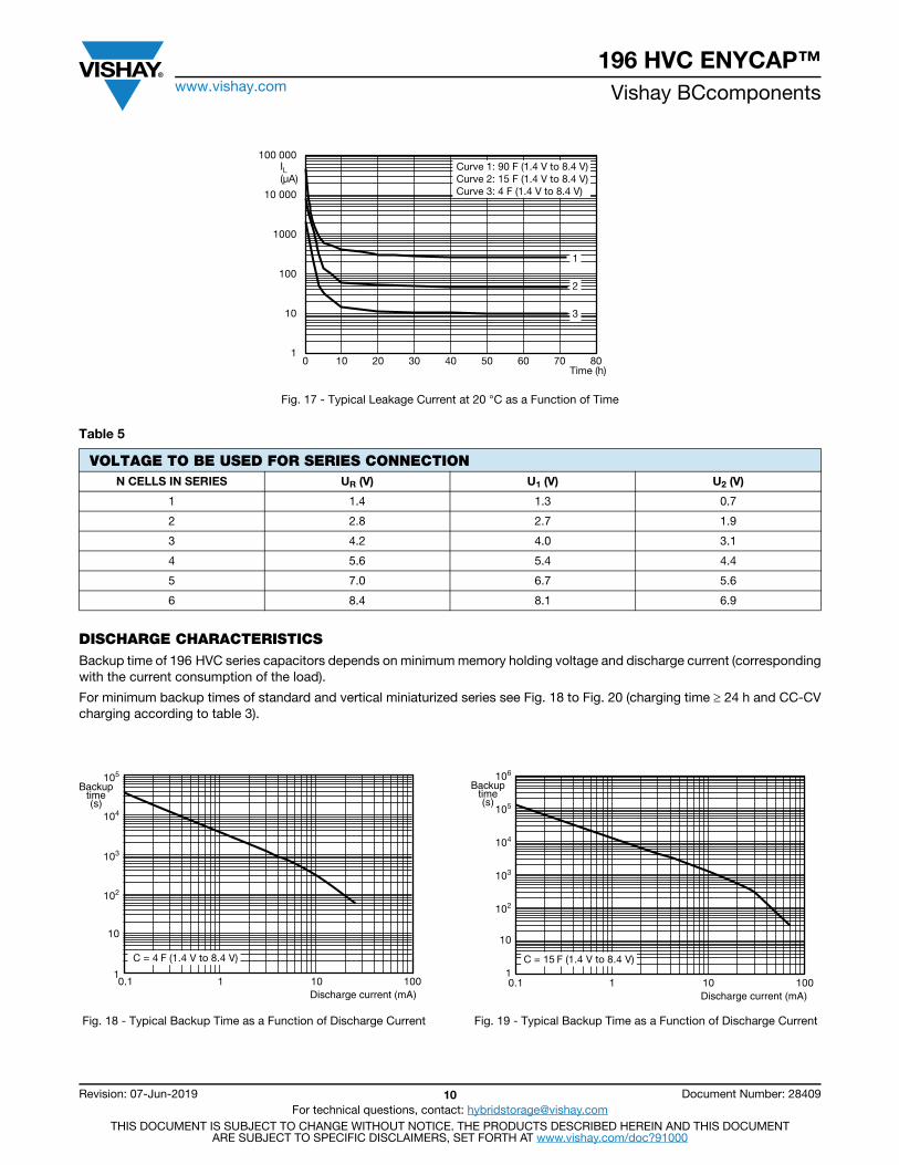
Fig. 17 - Typical Leakage Current at 20 °C as a Function of Time
Table 5
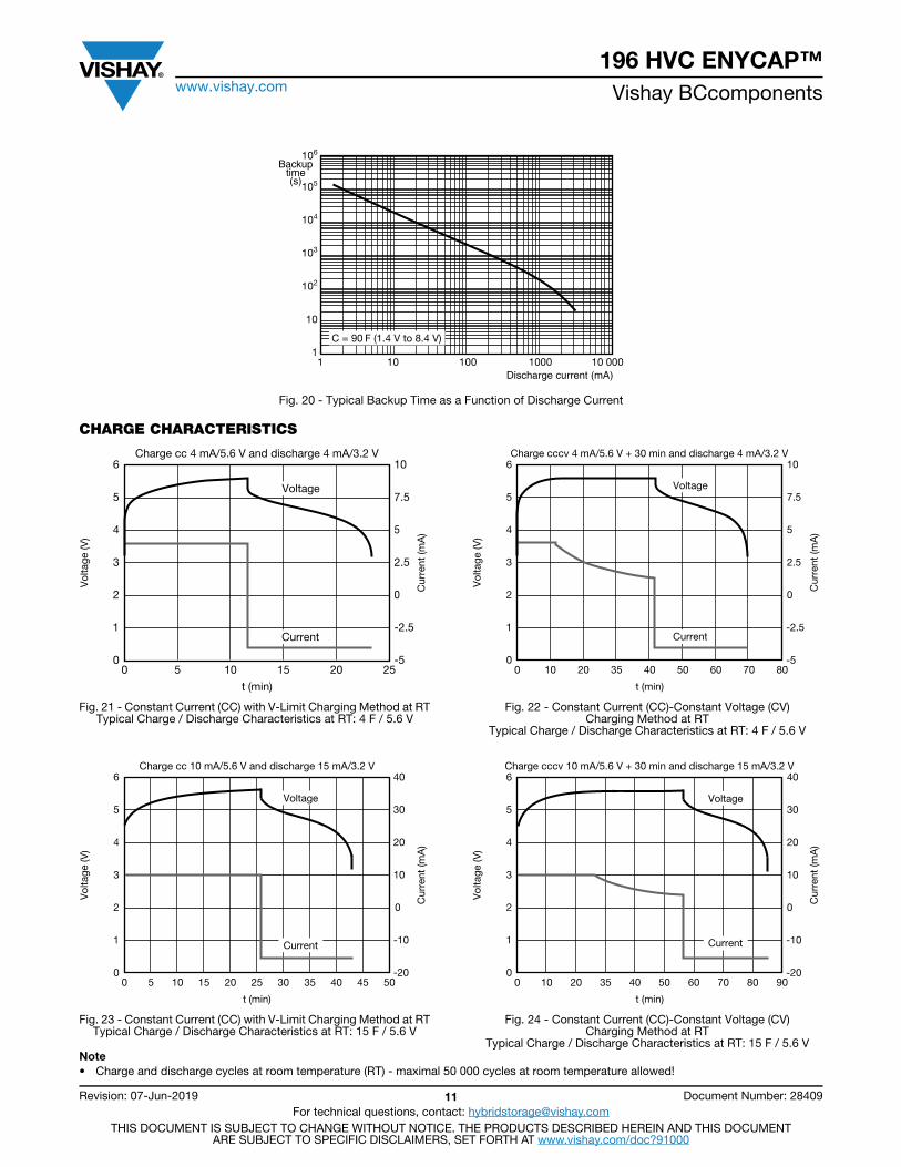
DISCHARGE CHARACTERISTICSBackup time of 196 HVC series capacitors depends on minimum memory holding voltage and discharge current (corresponding with the current consumption of the load).
For minimum backup times of standard and vertical miniaturized series see Fig. 18 to Fig. 20 (charging time 24 h and CC-CV charging according to table 3).
Fig. 18 - Typical Backup Time as a Function of Discharge Current Fig. 19 - Typical Backup Time as a Function of Discharge Current
VOLTAGE TO BE USED FOR SERIES CONNECTIONN CELLS IN SERIES UR (V) U1 (V) U2 (V)
1 1.4 1.3 0.7
2 2.8 2.7 1.9
3 4.2 4.0 3.1
4 5.6 5.4 4.4
5 7.0 6.7 5.6
6 8.4 8.1 6.9
1
10
100
1000
10 000
100 000
0 10 20 30 40 50 60 70 80
IL(μA)
Time (h)
3
2
1
Curve 1: 90 F (1.4 V to 8.4 V)Curve 2: 15 F (1.4 V to 8.4 V)Curve 3: 4 F (1.4 V to 8.4 V)
0.1 1 10 100Discharge current (mA)
C = 4 F (1.4 V to 8.4 V)
10
102
Backuptime(s)
1
103
104
105
10
102
0.1 1 10
Backuptime(s)
Discharge current (mA)
1
103
104
105
106
100
C = 15 F (1.4 V to 8.4 V)
196 HVC ENYCAP™www.vishay.com Vishay BCcomponents
Revision: 07-Jun-2019 11 Document Number: 28409For technical questions, contact: [email protected]
THIS DOCUMENT IS SUBJECT TO CHANGE WITHOUT NOTICE. THE PRODUCTS DESCRIBED HEREIN AND THIS DOCUMENTARE SUBJECT TO SPECIFIC DISCLAIMERS, SET FORTH AT www.vishay.com/doc?91000
Fig. 20 - Typical Backup Time as a Function of Discharge Current
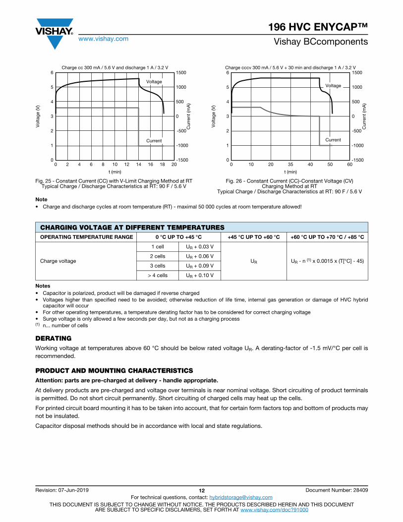
CHARGE CHARACTERISTICS
Fig. 21 - Constant Current (CC) with V-Limit Charging Method at RTTypical Charge / Discharge Characteristics at RT: 4 F / 5.6 V
Fig. 22 - Constant Current (CC)-Constant Voltage (CV)Charging Method at RT
Typical Charge / Discharge Characteristics at RT: 4 F / 5.6 V
Fig. 23 - Constant Current (CC) with V-Limit Charging Method at RTTypical Charge / Discharge Characteristics at RT: 15 F / 5.6 V
Fig. 24 - Constant Current (CC)-Constant Voltage (CV)Charging Method at RT
Typical Charge / Discharge Characteristics at RT: 15 F / 5.6 VNote• Charge and discharge cycles at room temperature (RT) - maximal 50 000 cycles at room temperature allowed!
10
102
1 10 100
Backuptime(s)
Discharge current (mA)
1
103
104
105
106
1000 10 000
C = 90 F (1.4 V to 8.4 V)
0
1
2
3
4
5
6
-5
-2.5
0
2.5
5
7.5
10
0 5 10 15 20 25
t (min)
Vol
tage
(V)
Cur
rent
(mA
)
Charge cc 4 mA/5.6 V and discharge 4 mA/3.2 V
Voltage
Current
0
1
2
3
4
5
6
-5
-2.5
0
2.5
5
7.5
10
0 10 20 35 40 50 60 70 80
t (min)
Vol
tage
(V)
Cur
rent
(mA
)
Charge cccv 4 mA/5.6 V + 30 min and discharge 4 mA/3.2 V
Voltage
Current
0
1
2
3
4
5
6
-20
-10
0
10
20
30
40
0 5 10 15 20 25 30 35 40 45 50
t (min)
Vol
tage
(V)
Cur
rent
(mA
)
Charge cc 10 mA/5.6 V and discharge 15 mA/3.2 V
Voltage
Current
0
1
2
3
4
5
6
-20
-10
0
10
20
30
40
0 10 20 35 40 50 60 70 80 90
t (min)
Voltage
Vol
tage
(V)
Cur
rent
(mA
)
Current
Charge cccv 10 mA/5.6 V + 30 min and discharge 15 mA/3.2 V
196 HVC ENYCAP™www.vishay.com Vishay BCcomponents
Revision: 07-Jun-2019 12 Document Number: 28409For technical questions, contact: [email protected]
THIS DOCUMENT IS SUBJECT TO CHANGE WITHOUT NOTICE. THE PRODUCTS DESCRIBED HEREIN AND THIS DOCUMENTARE SUBJECT TO SPECIFIC DISCLAIMERS, SET FORTH AT www.vishay.com/doc?91000
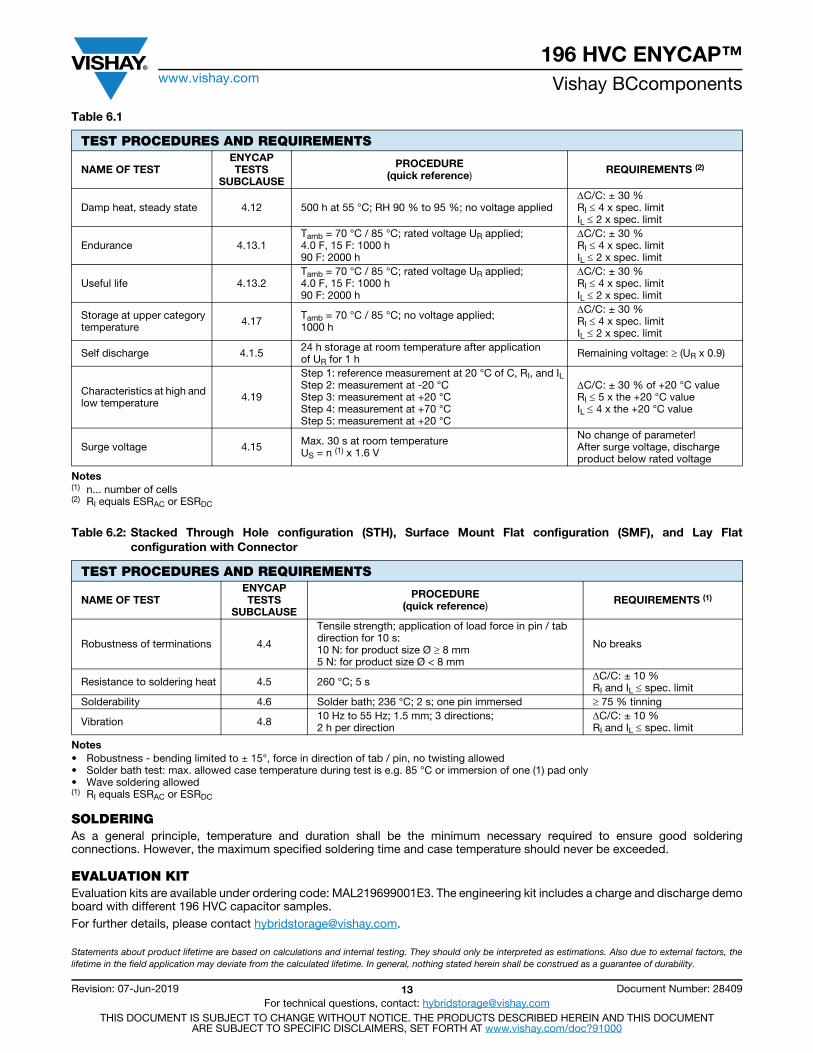
Fig. 25 - Constant Current (CC) with V-Limit Charging Method at RTTypical Charge / Discharge Characteristics at RT: 90 F / 5.6 V
Fig. 26 - Constant Current (CC)-Constant Voltage (CV)Charging Method at RT
Typical Charge / Discharge Characteristics at RT: 90 F / 5.6 V
Note• Charge and discharge cycles at room temperature (RT) - maximal 50 000 cycles at room temperature allowed!
Notes• Capacitor is polarized, product will be damaged if reverse charged• Voltages higher than specified need to be avoided; otherwise reduction of life time, internal gas generation or damage of HVC hybrid
capacitor will occur• For other operating temperatures, a temperature derating factor has to be considered for correct charging voltage• Surge voltage is only allowed a few seconds per day, but not as a charging process(1) n... number of cells
DERATINGWorking voltage at temperatures above 60 °C should be below rated voltage UR. A derating-factor of -1.5 mV/°C per cell is recommended.
PRODUCT AND MOUNTING CHARACTERISTICSAttention: parts are pre-charged at delivery - handle appropriate.
At delivery products are pre-charged and voltage over terminals is near nominal voltage. Short circuiting of product terminals is permitted. Do not short circuit permanently. Short circuiting of charged cells may heat up the cells.
For printed circuit board mounting it has to be taken into account, that for certain form factors top and bottom of products may not be insulated.
Capacitor disposal methods should be in accordance with local and state regulations.
0
1
2
3
4
5
6
-1500
-1000
-500
0
500
1000
1500
0 2 4 6 8 10 12 14 16 18 20
t (min)
Vol
tage
(V)
Cur
rent
(mA
)
Charge cc 300 mA / 5.6 V and discharge 1 A / 3.2 V
Voltage
Current
0
1
2
3
4
5
6
-1500
-1000
-500
0
500
1000
1500
0 10 20 35 40 50 60
t (min)
Vol
tage
(V)
Cur
rent
(mA
)
Charge cccv 300 mA / 5.6 V + 30 min and discharge 1 A / 3.2 V
Voltage
Current
CHARGING VOLTAGE AT DIFFERENT TEMPERATURESOPERATING TEMPERATURE RANGE 0 °C UP TO +45 °C +45 °C UP TO +60 °C +60 °C UP TO +70 °C / +85 °C
Charge voltage
1 cell UR + 0.03 V
UR UR - n (1) x 0.0015 x (T[°C] - 45)2 cells UR + 0.06 V
3 cells UR + 0.09 V
> 4 cells UR + 0.10 V
196 HVC ENYCAP™www.vishay.com Vishay BCcomponents
Revision: 07-Jun-2019 13 Document Number: 28409For technical questions, contact: [email protected]
THIS DOCUMENT IS SUBJECT TO CHANGE WITHOUT NOTICE. THE PRODUCTS DESCRIBED HEREIN AND THIS DOCUMENTARE SUBJECT TO SPECIFIC DISCLAIMERS, SET FORTH AT www.vishay.com/doc?91000
Table 6.1
Notes(1) n... number of cells(2) RI equals ESRAC or ESRDC
Table 6.2: Stacked Through Hole configuration (STH), Surface Mount Flat configuration (SMF), and Lay Flat configuration with Connector
Notes• Robustness - bending limited to ± 15°, force in direction of tab / pin, no twisting allowed• Solder bath test: max. allowed case temperature during test is e.g. 85 °C or immersion of one (1) pad only• Wave soldering allowed(1) RI equals ESRAC or ESRDC
SOLDERINGAs a general principle, temperature and duration shall be the minimum necessary required to ensure good soldering connections. However, the maximum specified soldering time and case temperature should never be exceeded.
EVALUATION KITEvaluation kits are available under ordering code: MAL219699001E3. The engineering kit includes a charge and discharge demo board with different 196 HVC capacitor samples.For further details, please contact [email protected] about product lifetime are based on calculations and internal testing. They should only be interpreted as estimations. Also due to external factors, the lifetime in the field application may deviate from the calculated lifetime. In general, nothing stated herein shall be construed as a guarantee of durability.
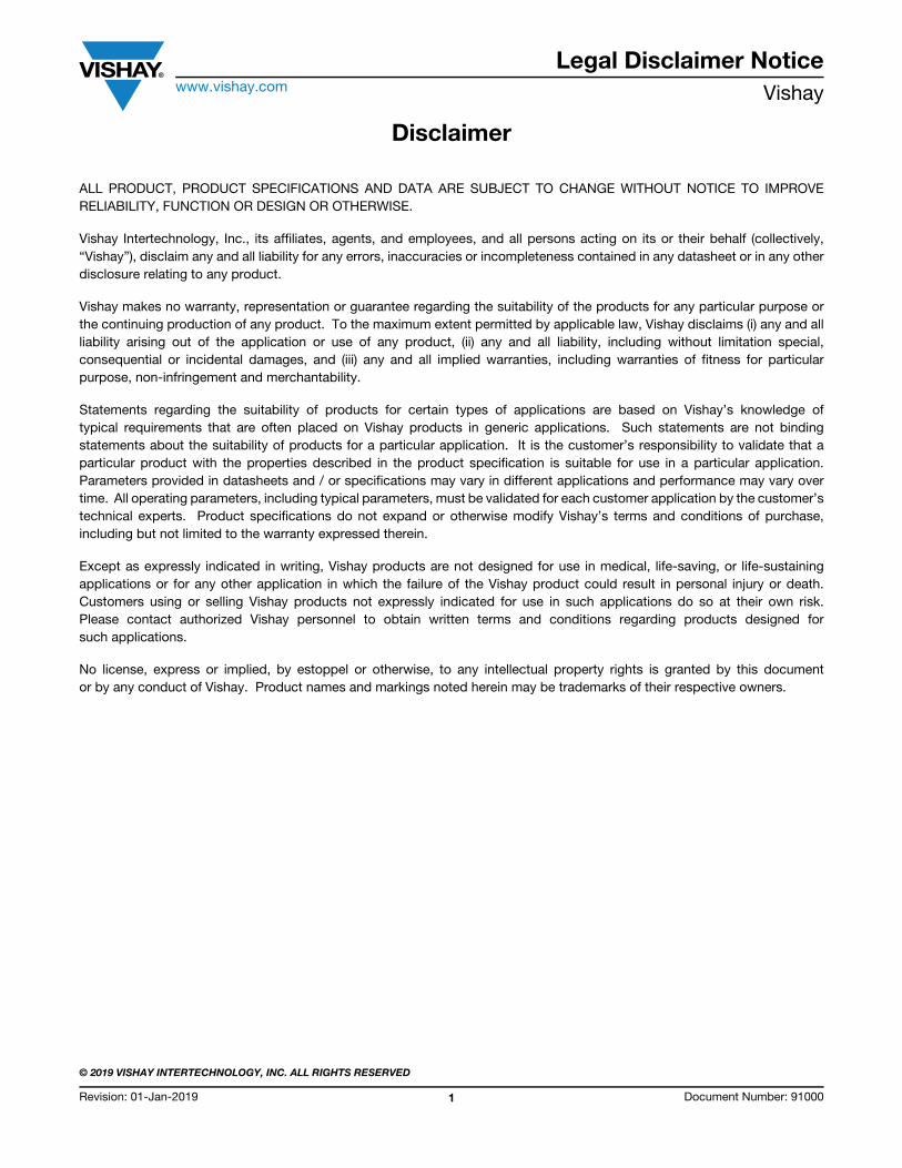
TEST PROCEDURES AND REQUIREMENTS
NAME OF TESTENYCAPTESTS
SUBCLAUSE
PROCEDURE(quick reference) REQUIREMENTS (2)
Damp heat, steady state 4.12 500 h at 55 °C; RH 90 % to 95 %; no voltage appliedC/C: ± 30 %RI 4 x spec. limitIL 2 x spec. limit
Endurance 4.13.1Tamb = 70 °C / 85 °C; rated voltage UR applied;4.0 F, 15 F: 1000 h90 F: 2000 h
C/C: ± 30 %RI 4 x spec. limitIL 2 x spec. limit
Useful life 4.13.2Tamb = 70 °C / 85 °C; rated voltage UR applied;4.0 F, 15 F: 1000 h90 F: 2000 h
C/C: ± 30 %RI 4 x spec. limitIL 2 x spec. limit
Storage at upper category temperature 4.17 Tamb = 70 °C / 85 °C; no voltage applied;
1000 h
C/C: ± 30 %RI 4 x spec. limitIL 2 x spec. limit
Self discharge 4.1.5 24 h storage at room temperature after applicationof UR for 1 h Remaining voltage: (UR x 0.9)
Characteristics at high and low temperature 4.19
Step 1: reference measurement at 20 °C of C, RI, and ILStep 2: measurement at -20 °CStep 3: measurement at +20 °CStep 4: measurement at +70 °CStep 5: measurement at +20 °C
C/C: ± 30 % of +20 °C valueRI 5 x the +20 °C valueIL 4 x the +20 °C value
Surge voltage 4.15 Max. 30 s at room temperatureUS = n (1) x 1.6 V
No change of parameter!After surge voltage, discharge product below rated voltage
TEST PROCEDURES AND REQUIREMENTS
NAME OF TESTENYCAPTESTS
SUBCLAUSE
PROCEDURE(quick reference) REQUIREMENTS (1)
Robustness of terminations 4.4
Tensile strength; application of load force in pin / tab direction for 10 s:10 N: for product size Ø 8 mm5 N: for product size Ø < 8 mm
No breaks
Resistance to soldering heat 4.5 260 °C; 5 s C/C: ± 10 %RI and IL spec. limit
Solderability 4.6 Solder bath; 236 °C; 2 s; one pin immersed 75 % tinning
Vibration 4.8 10 Hz to 55 Hz; 1.5 mm; 3 directions; 2 h per direction
C/C: ± 10 %RI and IL spec. limit
Legal Disclaimer Noticewww.vishay.com Vishay
Revision: 01-Jan-2019 1 Document Number: 91000
Disclaimer ALL PRODUCT, PRODUCT SPECIFICATIONS AND DATA ARE SUBJECT TO CHANGE WITHOUT NOTICE TO IMPROVE RELIABILITY, FUNCTION OR DESIGN OR OTHERWISE.
Vishay Intertechnology, Inc., its affiliates, agents, and employees, and all persons acting on its or their behalf (collectively, “Vishay”), disclaim any and all liability for any errors, inaccuracies or incompleteness contained in any datasheet or in any other disclosure relating to any product.
Vishay makes no warranty, representation or guarantee regarding the suitability of the products for any particular purpose or the continuing production of any product. To the maximum extent permitted by applicable law, Vishay disclaims (i) any and all liability arising out of the application or use of any product, (ii) any and all liability, including without limitation special, consequential or incidental damages, and (iii) any and all implied warranties, including warranties of fitness for particular purpose, non-infringement and merchantability.
Statements regarding the suitability of products for certain types of applications are based on Vishay’s knowledge of typical requirements that are often placed on Vishay products in generic applications. Such statements are not binding statements about the suitability of products for a particular application. It is the customer’s responsibility to validate that a particular product with the properties described in the product specification is suitable for use in a particular application. Parameters provided in datasheets and / or specifications may vary in different applications and performance may vary over time. All operating parameters, including typical parameters, must be validated for each customer application by the customer’s technical experts. Product specifications do not expand or otherwise modify Vishay’s terms and conditions of purchase, including but not limited to the warranty expressed therein.
Except as expressly indicated in writing, Vishay products are not designed for use in medical, life-saving, or life-sustaining applications or for any other application in which the failure of the Vishay product could result in personal injury or death. Customers using or selling Vishay products not expressly indicated for use in such applications do so at their own risk. Please contact authorized Vishay personnel to obtain written terms and conditions regarding products designed for such applications.
No license, express or implied, by estoppel or otherwise, to any intellectual property rights is granted by this document or by any conduct of Vishay. Product names and markings noted herein may be trademarks of their respective owners.
© 2019 VISHAY INTERTECHNOLOGY, INC. ALL RIGHTS RESERVED
Mouser Electronics
Authorized Distributor
Click to View Pricing, Inventory, Delivery & Lifecycle Information: Vishay:
MAL219691214E3 MAL219691124E3 MAL219691226E3 MAL219691105E3 MAL219691213E3 MAL219691223E3
MAL219691215E3 MAL219690103E3 MAL219691263E3 MAL219691201E3 MAL219691115E3 MAL219691202E3
MAL219691152E3 MAL219691102E3 MAL219691216E3 MAL219691116E3 MAL219691266E3 MAL219691104E3
MAL219691204E3 MAL219691154E3 MAL219691206E3 MAL219691212E3 MAL219691112E3 MAL219691222E3
MAL219691114E3 MAL219691123E3 MAL219691103E3 MAL219691265E3 MAL219691254E3 MAL219691153E3
MAL219691225E3 MAL219690102E3 MAL219691252E3 MAL219691211E3 MAL219691205E3 MAL219691203E3
MAL219691113E3 MAL219691101E3 MAL219691122E3 MAL219691126E3 MAL219691141E3 MAL219691224E3
MAL219691121E3 MAL219691106E3 MAL219691125E3 MAL219691253E3 MAL219690101E3 MAL219691261E3
MAL219691241E3 MAL219691264E3 MAL219691231E3 MAL219691131E3 MAL219691262E3 MAL219691111E3
MAL219691221E3 MAL219690201E3 MAL219690202E3 MAL219690112E3 MAL219690111E3 MAL219690113E3
MAL219690211E3 MAL219690106E3 MAL219695451E3 MAL219695602E3 MAL219695301E3 MAL219695302E3
MAL219695305E3 MAL219695605E3 MAL219695455E3 MAL219695452E3 MAL219695601E3 MAL219690213E3
MAL219690116E3 MAL219690107E3 MAL219690118E3 MAL219690212E3 MAL219690117E3 MAL219690108E3
MAL219690203E3 MAL219690998E3
Recommended