DRV8711
Stepper Motor Controller IC
CSD19538Q3A
Power MOSFETx8
MSP-EXP430G2LaunchPadTM
including MSP430G2553
15 V to 70 V
Current Sense
Gate Sense
Low-Voltage Gate Drive
GPIO
SPI
PWM
nFAULT
LM5017
12-V Buck Converter
15 V to 70 V
12 V
BOOST-DRV8711 GUI
Bipolar Stepper Motor
Low to High Voltage Interface
LM5107 x4CSD17483F4T
x8
High-Voltage Gate Drive
Copyright © 2016, Texas Instruments Incorporated
1TIDUCR6A–January 2017–Revised March 2017Submit Documentation Feedback
Copyright © 2017, Texas Instruments Incorporated
High-Voltage Stepper Reference Design Using DRV8711
TI DesignsHigh-Voltage Stepper Reference Design Using DRV8711
DescriptionThe TIDA-01227 reference design is a 15-V to 70-Vstepper motor controller for bipolar applications. Thedesign uses the following parts from Texas Instrument:DRV8711 bipolar stepper motor, controller gate driver;CSD19538Q3A 100-V, N-Channel NexFET™ powerMOSFETs; CSD17483F4 30-V, N-ChannelFemtoFET™ MOSFET; MSP430G2553 MCU; LM5107100-V, 1.4-A peak, half-bridge gate driver; andLM5017 12-V buck converter. The focus of this designis to demonstrate the use of the DRV8711 steppermotor controller to control stepper motors at voltageshigher than 60 V. The DRV8711 operates at 12 Vwhile using additional circuitry to convert to high-voltage control signals.
Resources
TIDA-01227 Design FolderDRV8711 Product FolderLM5107 Product FolderLM5017 Product FolderCSD19538Q3A Product FolderCSD17483F4T Product FolderMSP430™ LaunchPad™ Value-Line Development Kit Tool Folder
ASK Our E2E Experts
Features• 15-V to 70-V Input Voltage Range• 2-A RMS, 3-A Peak Output Current Capability• Designed to Use LaunchPad™ and Boost-
DRV8711 Software• Board Size: 2.3 in × 2.25 in• Onboard 12-V, 0.6-A Buck Converter• Wide Array of System Protection Features
Including DRV8711 Overtemperature and SupplyUndervoltage Protection
Applications• High-Speed Printers• High-Speed Industrial Steppers

System Overview www.ti.com
2 TIDUCR6A–January 2017–Revised March 2017Submit Documentation Feedback
Copyright © 2017, Texas Instruments Incorporated
High-Voltage Stepper Reference Design Using DRV8711
An IMPORTANT NOTICE at the end of this TI reference design addresses authorized use, intellectual property matters and otherimportant disclaimers and information.
1 System Overview
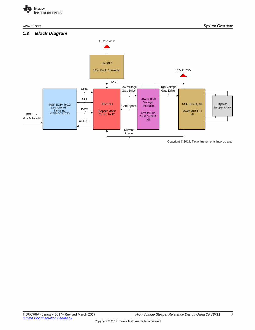
1.1 System DescriptionThe TIDA-01227 design configures the DRV8711 device to control a bipolar stepper motor at voltagesabove the absolute maximum voltage of the DRV8711. This configuration is possible by adding aninterface between the DRV8711 controller and the CSD19538Q3A field-effect transistors (FETs). Theinterface converts lower-voltage signals to higher-voltage signals controlling the full-bridges. Thisconfiguration can be used in applications that require high-speed operation. Higher voltage allows thecurrent to change at a faster rate, which increases the motor speed. A high-speed printer is an example ofa typical application.
The reference design is composed of three main sections: the MCU, the power stage, and the powerconversion sections.
The first section is the MCU, which decodes the commands from the graphical user interface (GUI) andsends the appropriate signals to the DRV8711 controller.
The second section is the power stage, which consists of the DRV8711 gate driver, the LM5107 half-bridge drivers, and the power MOSFETs. The LM5107 acts as an interface between the DRV8711 gatedriver and the power MOSFETs. The power stage amplifies the control signals from the MCU to the motorand regulates the current in the windings based on the settings in the configuration registers.
The third section is the power conversion section, which supplies power to the MOSFETs from the mainpower input. Power to the DRV8711 is supplied through a switching buck converter.
1.2 Key System Specifications
Table 1. Key System Specifications
PARAMETER SPECIFICATIONS DETAILSVoltage operation aboveabsolute maximum of DRV8711
System configured for 70-V operation; absolute maximum of the DRV8711 is60 V, recommended maximum is 52 V Section 2.1
Interface between DRV8711 andhigh-voltage FETs
Interface converts DRV8711 outputs from 0 V to 10/22 V into 0-V to 3.3-Vinputs at the LM5107 Section 2.1
12-V buck regulator Converts > 15 V to 12 V to provide power to the DRV8711 and LM5107bootstrap capacitors Section 2.1
DRV8711
Stepper Motor Controller IC
CSD19538Q3A
Power MOSFETx8
MSP-EXP430G2LaunchPadTM
including MSP430G2553
15 V to 70 V
Current Sense
Gate Sense
Low-Voltage Gate Drive
GPIO
SPI
PWM
nFAULT
LM5017
12-V Buck Converter
15 V to 70 V
12 V
BOOST-DRV8711 GUI
Bipolar Stepper Motor
Low to High Voltage Interface
LM5107 x4CSD17483F4T
x8
High-Voltage Gate Drive
Copyright © 2016, Texas Instruments Incorporated
www.ti.com System Overview
3TIDUCR6A–January 2017–Revised March 2017Submit Documentation Feedback
Copyright © 2017, Texas Instruments Incorporated
High-Voltage Stepper Reference Design Using DRV8711
1.3 Block Diagram

Over-
Temp
AOUT1
GND
RESET
Gate
Drive
&
OCP
Step
Motor
SCS
SCLK
VM
VM
SDATO
SDATI
SLEEPn
100 Fµ
+
0.01 Fµ
VM
PWM
logic
FAULTn
VINT
5V OUT
1 Fµ
CP1CP2 VCP
HS Gate DriveCharge
Pump
UVLO
PUCSTEP/AIN1
A1HSVM
A1LS
AOUT2
A2HSVM
A2LS
BOUT1
B1HSVM
B1LS
BOUT2
B2HSVM
B2LS
Gate
Drive
&
OCP
Gate
Drive
&
OCP
Gate
Drive
&
OCP
BISENP
ISEN
amp
+
-
AISENP
Comp
+
-
PWM
logic
STALLn / BEMFVn
DIR/AIN2
Reference
Stall detect BEMF
SIN
DAC
SIN
DAC
+
-
Comp
+
-
ISEN
amp
+
-
Comp
+
-
+
-
Comp
+
-
AISENN
BISENN
BIN1
BIN2
0.1 Fµ1 Fµ
Regs
V5
VM
1nF
0.1 Fµ
X
X
Torque
DAC
Torque
DAC
Logic
DCM
DCM
Copyright © 2017, Texas Instruments Incorporated
System Overview www.ti.com
4 TIDUCR6A–January 2017–Revised March 2017Submit Documentation Feedback
Copyright © 2017, Texas Instruments Incorporated
High-Voltage Stepper Reference Design Using DRV8711
1.4 Highlighted Products
1.4.1 DRV8711The DRV8711 device is a stepper motor controller that uses external N-channel MOSFETs to drive abipolar stepper motor or two brushed DC motors. A microstepping indexer is integrated, which is capableof step modes from full step to 1/256-step. Figure 1 shows the functional block diagram of the DRV8711device.
Figure 1. DRV8711 Functional Block Diagram

Clock
System
Brownout
Protection
RST/NMI
DVCC DVSS
MCLK
Watchdog
WDT+
15-Bit
Timer0_A3
3 CC
Registers
16MHz
CPU
incl. 16
Registers
Emulation
2BP
JTAG
Interface
SMCLK
ACLK
MDB
MAB
Port P1
8 I/O
Interrupt
capability
pullup/down
resistors
P1.x
8
P2.x
Port P2
8 I/O
Interrupt
capability
pullup/down
resistors
Spy-Bi-
Wire
Comp_A+
8 Channels
Timer1_A3
3 CC
Registers
XIN XOUT
Port P3
8 I/O
pullup/
pulldown
resistors
P3.x
8 8
RAM
512B
256B
Flash
16KB
8KB
4KB
2KB
USCI A0
UART/
LIN, IrDA,
SPI
USCI B0
SPI, I2C
ADC
10-Bit
8 Ch.
Autoscan
1 ch DMA
Copyright © 2017, Texas Instruments Incorporated
www.ti.com System Overview
5TIDUCR6A–January 2017–Revised March 2017Submit Documentation Feedback
Copyright © 2017, Texas Instruments Incorporated
High-Voltage Stepper Reference Design Using DRV8711
An ultra-smooth motion profile can be achieved using adaptive blanking time, adjustable decay times, andvarious current decay modes, including an auto-mixed decay mode. When microstepping, motor stall canbe reported with an optional back-electromotive force (back-EMF) output.
A simple step, direction, or pulse-width modulation (PWM) interface allows easy interfacing to controllercircuits. A serial peripheral interface (SPI) is used to program the device operation. Output current(torque), step mode, decay mode, and stall detection functions are all programmable through a SPI.
Internal shutdown functions are provided for overcurrent protection, short-circuit protection, undervoltagelockout, and overtemperature. Fault conditions are indicated through a FAULTn pin and each faultcondition is reported through a dedicated bit through SPI.
1.4.2 MSP430G2553The Texas Instruments MSP430™ family of ultra-low-power microcontrollers consists of several devicesfeaturing different sets of peripherals targeted for various applications. The architecture, combined withfive low-power modes, is optimized to achieve extended battery life in portable measurement applications.The device features a powerful 16-bit reduced instruction set computing (RISC) CPU, 16-bit registers, andconstant generators that contribute to maximum code efficiency. The digitally-controlled oscillator (DCO)allows wakeup from low-power modes to active mode in less than 1 μs.
Figure 2 shows the MSP430G2553 functional block diagram.
Figure 2. MSP430G2553 Functional Block Diagram
The MSP430G2x13 and MSP430G2x53 series are ultra-low-power mixed signal microcontrollers withbuilt-in 16-bit timers, up to 24 I/O capacitive-touch enabled pins, a versatile analog comparator, and built-in communication capability using the universal serial communication interface. In addition theMSP430G2x53 family members have a 10-bit ADC.
Typical applications include low-cost sensor systems that capture analog signals, convert them to digitalvalues, and then process the data for display or for transmission to a host system.

DRIVER
DRIVER
LEVELSHIFT
UVLO
UVLO
HI
VDD
LI
VSS
HB
HO
HS
LO
HV
Copyright © 2016, Texas Instruments Incorporated
System Overview www.ti.com
6 TIDUCR6A–January 2017–Revised March 2017Submit Documentation Feedback
Copyright © 2017, Texas Instruments Incorporated
High-Voltage Stepper Reference Design Using DRV8711
1.4.3 LM5107The LM5107 is designed to drive both the high-side and the low-side N-channel FETs in a synchronousbuck or a half-bridge configuration. The outputs are independently controlled with transistor-transistor logic(TTL) input thresholds. The floating high-side driver is capable of working with supply voltages up to100 V. An integrated high-voltage diode is provided to charge the high-side gate drive bootstrap capacitor.A robust level shifter operates at high speed while consuming low power and providing clean leveltransitions from the control logic to the high-side gate driver. Undervoltage lockout is provided on both thelow-side and the high-side power rails.
Figure 3 shows the LM5107 functional block diagram.
Figure 3. LM5107 Functional Block Diagram
1.4.4 LM5017The LM5017 step-down switching regulator features all the functions required to implement a low-cost,efficient, buck converter capable of supplying up to 0.6 A to the load. This high-voltage regulator containsa 100-V N-channel buck and synchronous switches, is easy to implement, and is provided in thermally-enhanced HSOP PowerPAD-8 and WSON-8 packages. The regulator operation is based on a constanton-time control scheme using an on-time inversely proportional to VIN. This control scheme does notrequire loop compensation. The current limit is implemented with a forced off-time inversely proportional toVOUT. This scheme ensures short-circuit protection while providing minimum foldback.
The LM5017 can be applied in numerous applications to efficiently downregulate higher voltages. Thisregulator is well-suited for 48-V telecom and automotive power bus ranges.
Figure 4 shows the LM5017 functional block diagram.

FB
VINVCC
SW
RTN
BST
1.225V
VILIM
LM5017
RON
ILIMCOMPARATOR
+
-
V UVLO
ON/OFF
TIMERS
COT CONTROL
LOGIC
1.225V
START-UP
REGULATOR
VIN
FEEDBACK
DISABLE
THERMAL
SHUTDOWN
UVLO
OVER-VOLTAGE1.62V
UVLO
4.5V
SD
SHUTDOWN
VDD REG
BG REF
0.66V
20 µA
CURRENT
LIMIT
ONE-SHOT
Copyright © 2017, Texas Instruments Incorporated
www.ti.com System Overview
7TIDUCR6A–January 2017–Revised March 2017Submit Documentation Feedback
Copyright © 2017, Texas Instruments Incorporated
High-Voltage Stepper Reference Design Using DRV8711
Figure 4. LM5017 Functional Block Diagram

1 D
2 D
3 D
4
D
D5G
6S
7S
8S
P0093-01
D
G S
System Overview www.ti.com
8 TIDUCR6A–January 2017–Revised March 2017Submit Documentation Feedback
Copyright © 2017, Texas Instruments Incorporated
High-Voltage Stepper Reference Design Using DRV8711
1.4.5 CSD17483F4TThis 200-mΩ, 30-V N-Channel FemtoFET™ MOSFET technology is designed and optimized to minimizethe footprint in many handheld and mobile applications. This technology is capable of replacing standardsmall-signal MOSFETs while providing at least a 60% reduction in footprint size.
Figure 5 shows the top view of the CSD17483F4T MOSFET.
Figure 5. CSD17438F4 Top View
1.4.6 CSD19538Q3AThis 100-V, 49-mΩ, SON 3.3-mm × 3.3-mm NexFET™ power MOSFET is designed to minimizeconduction losses and reduce board footprint in Power-over-Ethernet (PoE) applications.
Figure 6 shows the top view of the CSD19538Q3A MOSFET.
Figure 6. CSD19538Q3A Top View

CP11
CP22
VCP3
VM4
GND5
V56
VINT7
SLEEP8
RESET9
STEP/AIN110
DIR/AIN211
BIN112
BIN213
SCLK14
SDATI15
SCS16
SDATO17
FAULT18
STALL/BEMFV19
BEMF20
BOUT221
B2HS22
B2LS23
BISENN24
BISENP25
B1LS26
B1HS27
BOUT128
GND29
AOUT230
A2HS31
A2LS32
AISENN33
AISENP34
A1LS35
A1HS36
AOUT137
GND38
PAD39
U2
DRV8711DCPR
CP1
CP2
nSLEEPRESETSTEP/AIN1DIR/AIN2
BIN1BIN2
SCLK
SDATISCS
SDATO
nFAULT
nSTALL
3.3kR8
330R11
330R10
GND
3.3V
BEMF
AOUT1
A1HS
A1LS
AISENPAISENN
A2LS
A2HS
AOUT2
BOUT1
B1HS
B1LS
BISENP
BISENN
B2LS
B2HS
BOUT2
V12
GND
0.1µF
C12
1µFC9
V12
V5
VINT
VCP
1µF
C11
1000pFC14
RedD1
Red
D2
1µF
C13
0.1µFC10
Copyright © 2017, Texas Instruments Incorporated
www.ti.com System Design Theory
9TIDUCR6A–January 2017–Revised March 2017Submit Documentation Feedback
Copyright © 2017, Texas Instruments Incorporated
High-Voltage Stepper Reference Design Using DRV8711
2 System Design TheoryThe MSP430G2 LaunchPad, containing a MSP430G2553 device, has been configured to act as theinterface between the BOOST-DRV8711 GUI and the DRV8711 device. The 3.3-V power supply issupplied from the computer through the USB connector.
2.1 Hardware Design TheoryTIDA-01227 is designed to spin stepper motors at high rates of speed. In some applications, this actioncan only be achieved by increasing the system voltage used to regulate the current. As the motor speedincreases and the back-electromotive force of the motor increases, the rate of change in current is limited.By increasing the system voltage, the rate of change in current can be increased and the speed of themotor can be increased.
This design has been tested to 70 V with 2-A current full-scale. With different components, the design canbe extended to higher voltages. Although not added for this reference design, consider placing a thermalcircuit near the FETs to monitor the operating temperature of the FETs.
The MSP430G2 LaunchPad, containing a MSP430G2553 device, has been configured to act as theinterface between the BOOST-DRV8711 GUI and the DRV8711 device. The 3.3-V power supply issupplied from the computer through the USB connector.
Figure 7 shows the schematic for the DRV8711 block.
Figure 7. DRV8711 Block
0.05R9
GND
NT2
Net-Tie
NT1
Net-Tie
AISENN
AISENP GND_A
7,8
1,2
,3
5,6
,
Q4CSD19538Q3A 7
,81
,2,3
5,6
, Q3CSD19538Q3A
7,8
1,2
,3
5,6
, Q1CSD19538Q3A
7,8
1,2
,3
5,6
,
Q2CSD19538Q3A
A1HS_MOT
AOUT1_MOT
A1LS_MOT
A2HS_MOT
AOUT2_MOT
A2LS_MOT
Bridge VM
0.1µFC23
0.1µFC24
GND
Copyright © 2017, Texas Instruments Incorporated
System Design Theory www.ti.com
10 TIDUCR6A–January 2017–Revised March 2017Submit Documentation Feedback
Copyright © 2017, Texas Instruments Incorporated
High-Voltage Stepper Reference Design Using DRV8711
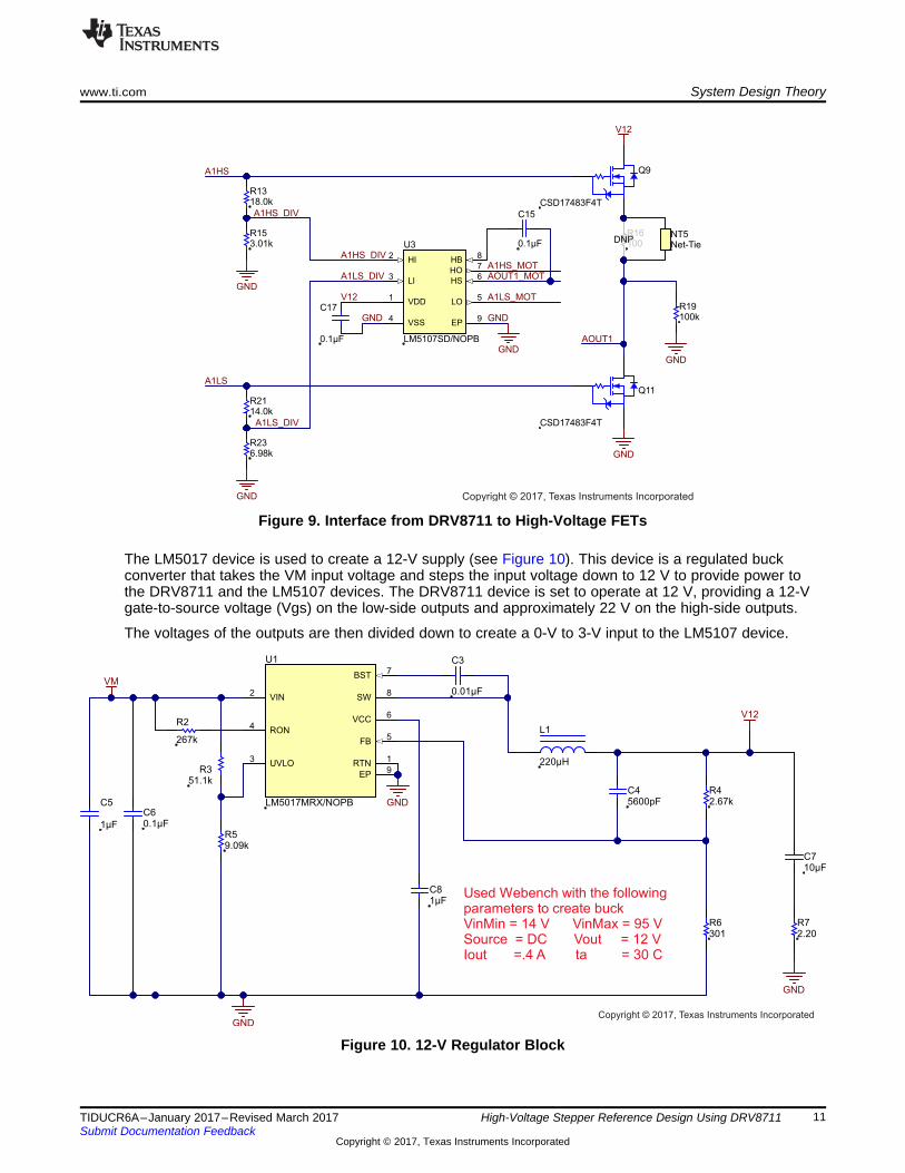
The DRV8711 stepper motor controller sends the commands to the LM5107 device through a voltagedivider. The ALSx and BLSx output pins of the DRV8711 device toggle from 0 V to 10 V. These signalsare then divided to 0 V to 3.3 V using a 3:1 attenuation network. The AHSx and BHSx output pins togglefrom 0 V to 22 V and are divided down to 0 V to 3.3 V with a 7:1 attenuation network. The integrated-microstepping indexer is capable of step modes from full-step to 1/256-step.
The internal current shunt amplifiers are referenced to the internal reference voltage and adjusted usingthe TORQUE setting, gain, and indexer table. The STEP and DIR pins control the indexer table. As theSTEP pin transitions from a logic low to high, the indexer changes to the next state. The nSLEEP pin isused to wake the device from its low-power sleep mode.
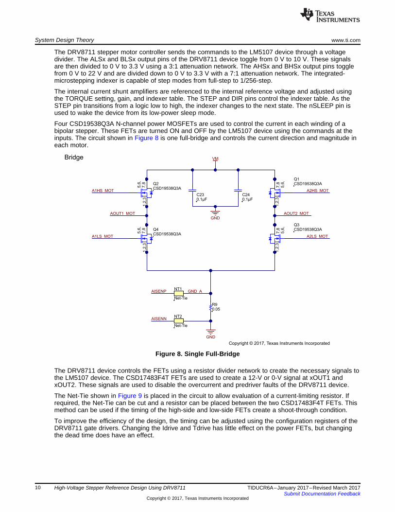
Four CSD19538Q3A N-channel power MOSFETs are used to control the current in each winding of abipolar stepper. These FETs are turned ON and OFF by the LM5107 device using the commands at theinputs. The circuit shown in Figure 8 is one full-bridge and controls the current direction and magnitude ineach motor.
Figure 8. Single Full-Bridge
The DRV8711 device controls the FETs using a resistor divider network to create the necessary signals tothe LM5107 device. The CSD17483F4T FETs are used to create a 12-V or 0-V signal at xOUT1 andxOUT2. These signals are used to disable the overcurrent and predriver faults of the DRV8711 device.
The Net-Tie shown in Figure 9 is placed in the circuit to allow evaluation of a current-limiting resistor. Ifrequired, the Net-Tie can be cut and a resistor can be placed between the two CSD17483F4T FETs. Thismethod can be used if the timing of the high-side and low-side FETs create a shoot-through condition.
To improve the efficiency of the design, the timing can be adjusted using the configuration registers of theDRV8711 gate drivers. Changing the Idrive and Tdrive has little effect on the power FETs, but changingthe dead time does have an effect.
VM
GND
V12
267k
R2
51.1kR3
2.67kR4
1µF
C5
0.1µFC6
5600pFC4
2.20R7
GND
220µH
L1
0.01µF
C3
10µFC7
Used Webench with the followingparameters to create buckVinMin = 14 V VinMax = 95 VSource = DC Vout = 12 VIout =.4 A ta = 30 C
RTN1
VIN2
UVLO3
RON4
FB5
VCC6
BST7
SW8
EP9
U1
LM5017MRX/NOPB GND
9.09kR5
301R6
1µFC8
Copyright © 2017, Texas Instruments Incorporated
AOUT1
GND
A1HS
A1LS
V12
Q11
CSD17483F4T
100kR19
GND
Q9
CSD17483F4T
NT5Net-Tie
18.0kR13
3.01kR15
6.98kR23
14.0kR21
GND
GND
A1LS_DIV
A1HS_DIV
VSS4
VDD1
HO7
LO5
HI2
HB8
LI3
HS6
EP9
U3
LM5107SD/NOPB
V12
GNDGND
AOUT1_MOT
A1HS_DIV
A1LS_DIV
A1LS_MOT
A1HS_MOT
0.1µF
C17
GND
100R16
DNP0.1µF
C15
Copyright © 2017, Texas Instruments Incorporated
www.ti.com System Design Theory
11TIDUCR6A–January 2017–Revised March 2017Submit Documentation Feedback
Copyright © 2017, Texas Instruments Incorporated
High-Voltage Stepper Reference Design Using DRV8711
Figure 9. Interface from DRV8711 to High-Voltage FETs
The LM5017 device is used to create a 12-V supply (see Figure 10). This device is a regulated buckconverter that takes the VM input voltage and steps the input voltage down to 12 V to provide power tothe DRV8711 and the LM5107 devices. The DRV8711 device is set to operate at 12 V, providing a 12-Vgate-to-source voltage (Vgs) on the low-side outputs and approximately 22 V on the high-side outputs.
The voltages of the outputs are then divided down to create a 0-V to 3-V input to the LM5107 device.
Figure 10. 12-V Regulator Block

VM
GND
0.1µFC2 100µF
C1
J4
Copyright © 2017, Texas Instruments Incorporated
System Design Theory www.ti.com
12 TIDUCR6A–January 2017–Revised March 2017Submit Documentation Feedback
Copyright © 2017, Texas Instruments Incorporated
High-Voltage Stepper Reference Design Using DRV8711
The power supply is connected directly to the board and filtered with a 100-µF bulk electrolytic capacitor(see Figure 11).
Figure 11. Power Connections
2.2 Software Design TheoryThe motor controller uses the BOOST-DRV8711 GUI and firmware. This code can be loaded and controlthe stepper when configured as shown in the Configuring the LaunchPad, Introduction, Setting up theBOOST-DRV8711 Firmware, and Setting up the BOOST-DRV8711 GUI sections of the BOOST-DRV8711User's Guide [1]. Refer to this BOOST-DRV8711 User’s Guide [1] for instructions on loading the firmwareinto the LaunchPad. When loaded, refer to the user's guide for instructions on how to install and open theGUI.
After the GUI is open, use the instructions in Section 3 to control the stepper. The GUI sets the decaymode, max current, gate drive timing, microstep mode, and other key parameters to operate the steppermotor.

www.ti.com Getting Started Hardware and Software
13TIDUCR6A–January 2017–Revised March 2017Submit Documentation Feedback
Copyright © 2017, Texas Instruments Incorporated
High-Voltage Stepper Reference Design Using DRV8711
3 Getting Started Hardware and Software
3.1 HardwareTo operate TIDA-01227, a LaunchPad must be connected to the board. The LaunchPad requires theBOOST-DRV8711 firmware to be loaded. The BOOST-DRV8711 GUI can be used to control the motor.The specified power must be > 15 V and < 70 V and the motor must be connected.
The circuit has been tested to 70 V and with 2-A full-scale current.
3.2 ConnectionsThe TIDA-01227 reference design can be powered from a 15-V to 70-V power supply. The supply isconnected to the printed-circuit board (PCB) through the VM and GND connections on the J4 connector.The motor is connected to the PCB through the J3 connector. The PCB is connected to the LaunchPadthrough connectors J1 and J2.
The speed, microstep mode, chopping current, and other key parameters are controlled by the GUI.
3.3 ProcedureRefer to the following steps to get started with the reference design hardware:1. Connect the power supply to the design through the J4 connector.2. Connect the motor to the design through the J3 connector.3. Program the LaunchPad with the BOOST-DRV8711 firmware.4. Attach the LaunchPad, enable the power supply, and open the GUI.5. Set the GUI controls to mirror the specifications in Figure 12 and Figure 13.
Figure 12. GUI Front Panel Settings

Getting Started Hardware and Software www.ti.com
14 TIDUCR6A–January 2017–Revised March 2017Submit Documentation Feedback
Copyright © 2017, Texas Instruments Incorporated
High-Voltage Stepper Reference Design Using DRV8711
Figure 13. GUI Register Settings
3.4 SoftwareTIDA-01227 uses the BOOST-DRV8711 GUI to control the bipolar stepper motor. The firmware and GUI,along with installation instructions, is located in the BOOST-DRV8711 tool folder.

www.ti.com Testing and Results
15TIDUCR6A–January 2017–Revised March 2017Submit Documentation Feedback
Copyright © 2017, Texas Instruments Incorporated
High-Voltage Stepper Reference Design Using DRV8711
4 Testing and ResultsThe following equipment was used during the testing of the reference design (see Figure 14):• DC power supply Chroma 620012P-100-50• Multimeter Tektronix DMM 4040• Oscilloscope Tektronix DPO 7054
Figure 14. Bench Setup
Data was collected at 24 V and 48 V to highlight the difference in current available at higher voltages (seeFigure 15). The motor is being operated at 40k steps per seconds, 1/32 microsteps, and 2-A full-scalecurrent.

Testing and Results www.ti.com
16 TIDUCR6A–January 2017–Revised March 2017Submit Documentation Feedback
Copyright © 2017, Texas Instruments Incorporated
High-Voltage Stepper Reference Design Using DRV8711
Figure 15. 40k PPS, 24 V, 2-A Full-Scale, 1/32 Microstep Mode
At 24V, the normal current sine wave has collapsed and the current is no longer able to reach the full-scale target of 2 A (see Figure 16). The current only reaches 1.35 A.
Figure 16. 40k PPS, 48 V, 2-A Full-Scale, 1/32 Microstep Mode

www.ti.com Testing and Results
17TIDUCR6A–January 2017–Revised March 2017Submit Documentation Feedback
Copyright © 2017, Texas Instruments Incorporated
High-Voltage Stepper Reference Design Using DRV8711
At 48 V the sine wave has degraded, but current is able to reach the full-scale target of 2 A.
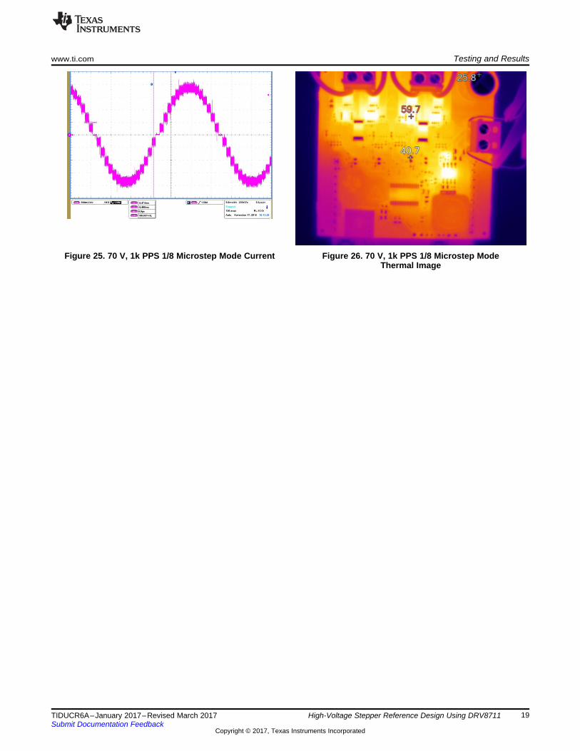
The following data in Figure 17 through Figure 26 was collected from 30 V to 70 V in 10-V increments.The stepper was operated in 1/8 microstep mode and the step input was toggled at 1k steps per second.
Figure 17. 30 V, 1k PPS 1/8 Microstep Mode Current Figure 18. 30 V, 1k PPS 1/8 Microstep ModeThermal Image
Figure 19. 40 V, 1k PPS 1/8 Microstep Mode Current Figure 20. 40 V, 1k PPS 1/8 Microstep ModeThermal Image

Testing and Results www.ti.com
18 TIDUCR6A–January 2017–Revised March 2017Submit Documentation Feedback
Copyright © 2017, Texas Instruments Incorporated
High-Voltage Stepper Reference Design Using DRV8711
Figure 21. 50 V, 1k PPS 1/8 Microstep Mode Current Figure 22. 50 V, 1k PPS 1/8 Microstep ModeThermal Image
Figure 23. 6 0V, 1k PPS 1/8 Microstep Mode Current Figure 24. 60 V, 1k PPS 1/8 Microstep ModeThermal Image
www.ti.com Testing and Results
19TIDUCR6A–January 2017–Revised March 2017Submit Documentation Feedback
Copyright © 2017, Texas Instruments Incorporated
High-Voltage Stepper Reference Design Using DRV8711
Figure 25. 70 V, 1k PPS 1/8 Microstep Mode Current Figure 26. 70 V, 1k PPS 1/8 Microstep ModeThermal Image

Design Files www.ti.com
20 TIDUCR6A–January 2017–Revised March 2017Submit Documentation Feedback
Copyright © 2017, Texas Instruments Incorporated
High-Voltage Stepper Reference Design Using DRV8711
5 Design Files
5.1 SchematicsTo download the schematics, see the design files at TIDA-01227.
5.2 Bill of MaterialsTo download the bill of materials (BOM), see the design files at TIDA-01227.
5.3 PCB Layout Recommendations
5.3.1 Layout PrintsTo download the layer plots, see the design files at TIDA-01227.
5.4 Altium ProjectTo download the Altium project files, see the design files at TIDA-01227.
5.5 Gerber FilesTo download the Gerber files, see the design files at TIDA-01227.
5.6 Assembly DrawingsTo download the assembly drawings, see the design files at TIDA-01227.
6 Software FilesTo download the software files, see the design files at TIDA-01227.
7 Related Documentation
1. Texas Instruments, DRV8711EVM User’s Guide, DRV8711EVM User's Guide (SLVA637)2. Texas Instruments, DRV8711 Decay Mode Setting Optimization, DRV8711 Application Report
(SLVA637)3. Texas Instruments, DRV8711 Quick Spin and Tuning Guide, DRV8711 Application Report (SLVA632)
7.1 TrademarksNexFET, FemtoFET, MSP430, LaunchPad are trademarks of Texas Instruments.All other trademarks are the property of their respective owners.
8 Terminology
MCU— Microcontroller
NetTie— Schematic element that allows two net names to be connected. In the layout, the NetTie is apiece of metal.
PPS— Pulses per second applied at the STEP input of the DRV8711
9 About the AuthorRICK DUNCAN is an Applications Engineer for Texas Instrument’s motor drive business, where he isresponsible for supporting TI’s motor drive portfolio. Rick graduated from Louisiana State University with abachelor’s of science in Electrical Engineering.

www.ti.com Revision History A
21TIDUCR6A–January 2017–Revised March 2017Submit Documentation Feedback
Copyright © 2017, Texas Instruments Incorporated
Revision History
Revision History ANOTE: Page numbers for previous revisions may differ from page numbers in the current version.
Changes from Original (January 2017) to A Revision .................................................................................................... Page
• Changed "ALSx and BLS output pins" to "ALSx and BLSx output pins" ......................................................... 10

IMPORTANT NOTICE FOR TI DESIGN INFORMATION AND RESOURCES
Texas Instruments Incorporated (‘TI”) technical, application or other design advice, services or information, including, but not limited to,reference designs and materials relating to evaluation modules, (collectively, “TI Resources”) are intended to assist designers who aredeveloping applications that incorporate TI products; by downloading, accessing or using any particular TI Resource in any way, you(individually or, if you are acting on behalf of a company, your company) agree to use it solely for this purpose and subject to the terms ofthis Notice.TI’s provision of TI Resources does not expand or otherwise alter TI’s applicable published warranties or warranty disclaimers for TIproducts, and no additional obligations or liabilities arise from TI providing such TI Resources. TI reserves the right to make corrections,enhancements, improvements and other changes to its TI Resources.You understand and agree that you remain responsible for using your independent analysis, evaluation and judgment in designing yourapplications and that you have full and exclusive responsibility to assure the safety of your applications and compliance of your applications(and of all TI products used in or for your applications) with all applicable regulations, laws and other applicable requirements. Yourepresent that, with respect to your applications, you have all the necessary expertise to create and implement safeguards that (1)anticipate dangerous consequences of failures, (2) monitor failures and their consequences, and (3) lessen the likelihood of failures thatmight cause harm and take appropriate actions. You agree that prior to using or distributing any applications that include TI products, youwill thoroughly test such applications and the functionality of such TI products as used in such applications. TI has not conducted anytesting other than that specifically described in the published documentation for a particular TI Resource.You are authorized to use, copy and modify any individual TI Resource only in connection with the development of applications that includethe TI product(s) identified in such TI Resource. NO OTHER LICENSE, EXPRESS OR IMPLIED, BY ESTOPPEL OR OTHERWISE TOANY OTHER TI INTELLECTUAL PROPERTY RIGHT, AND NO LICENSE TO ANY TECHNOLOGY OR INTELLECTUAL PROPERTYRIGHT OF TI OR ANY THIRD PARTY IS GRANTED HEREIN, including but not limited to any patent right, copyright, mask work right, orother intellectual property right relating to any combination, machine, or process in which TI products or services are used. Informationregarding or referencing third-party products or services does not constitute a license to use such products or services, or a warranty orendorsement thereof. Use of TI Resources may require a license from a third party under the patents or other intellectual property of thethird party, or a license from TI under the patents or other intellectual property of TI.TI RESOURCES ARE PROVIDED “AS IS” AND WITH ALL FAULTS. TI DISCLAIMS ALL OTHER WARRANTIES ORREPRESENTATIONS, EXPRESS OR IMPLIED, REGARDING TI RESOURCES OR USE THEREOF, INCLUDING BUT NOT LIMITED TOACCURACY OR COMPLETENESS, TITLE, ANY EPIDEMIC FAILURE WARRANTY AND ANY IMPLIED WARRANTIES OFMERCHANTABILITY, FITNESS FOR A PARTICULAR PURPOSE, AND NON-INFRINGEMENT OF ANY THIRD PARTY INTELLECTUALPROPERTY RIGHTS.TI SHALL NOT BE LIABLE FOR AND SHALL NOT DEFEND OR INDEMNIFY YOU AGAINST ANY CLAIM, INCLUDING BUT NOTLIMITED TO ANY INFRINGEMENT CLAIM THAT RELATES TO OR IS BASED ON ANY COMBINATION OF PRODUCTS EVEN IFDESCRIBED IN TI RESOURCES OR OTHERWISE. IN NO EVENT SHALL TI BE LIABLE FOR ANY ACTUAL, DIRECT, SPECIAL,COLLATERAL, INDIRECT, PUNITIVE, INCIDENTAL, CONSEQUENTIAL OR EXEMPLARY DAMAGES IN CONNECTION WITH ORARISING OUT OF TI RESOURCES OR USE THEREOF, AND REGARDLESS OF WHETHER TI HAS BEEN ADVISED OF THEPOSSIBILITY OF SUCH DAMAGES.You agree to fully indemnify TI and its representatives against any damages, costs, losses, and/or liabilities arising out of your non-compliance with the terms and provisions of this Notice.This Notice applies to TI Resources. Additional terms apply to the use and purchase of certain types of materials, TI products and services.These include; without limitation, TI’s standard terms for semiconductor products http://www.ti.com/sc/docs/stdterms.htm), evaluationmodules, and samples (http://www.ti.com/sc/docs/sampterms.htm).
Mailing Address: Texas Instruments, Post Office Box 655303, Dallas, Texas 75265Copyright © 2017, Texas Instruments Incorporated
Recommended