This is information on a product in full production.
January 2014 DocID8190 Rev 8 1/13
HCF4010
Hex buffer/converter (non-inverting)
Datasheet - production data
Features
• Propagation delay time
– tPD = 50 ns (typ.) at VDD = 10 V, CL = 50 pF
• High to low level logic conversion
• Multiplexer: 1 to 6 or 6 to 1
• High “sink” and “source” current capability
• Quiescent current specified up to 20 V
• 5 V, 10 V and 15 V parametric ratings
• Input leakage current
• II = 100 nA (max.) at VDD = 18 V, TA = 25 °C 100% tested for quiescent current
• ESD performance
– CDM: 1 kV
– HBM: 1 kV
– MM: 150 V
Applications
• Automotive
• Industrial
• Computer
• Consumer
Description
The HCF4010 device is a monolithic integrated circuit fabricated in MOS (metal oxide semiconductor) technology available in an SO16 package.
It is a non-inverting hex buffer/converter and can be used as a CMOS to TTL logic level converter, as a current “sink” or “source” driver, or as a multiplexer (1 to 6).
It is the preferred replacement of the HCF4050B in buffer applications.
SO16
Table 1. Device summary
Order code Temperature range Package Packing Marking
HCF4010M013TR –55 °C to +125 °C SO16Tape and reel
HCF4010
HCF4010YM013TR(1) –40 °C to +125 °C SO16 (automotive grade) HCF4010Y
1. Qualification and characterization according to AEC Q100 and Q003 or equivalent, advanced screening according to AEC Q001 and Q002 or equivalent.
www.st.com

Contents HCF4010
2/13 DocID8190 Rev 8
Contents
1 Pin information . . . . . . . . . . . . . . . . . . . . . . . . . . . . . . . . . . . . . . . . . . . . . 3
2 Functional description . . . . . . . . . . . . . . . . . . . . . . . . . . . . . . . . . . . . . . . 4
3 Electrical characteristics . . . . . . . . . . . . . . . . . . . . . . . . . . . . . . . . . . . . . 5
4 Package information . . . . . . . . . . . . . . . . . . . . . . . . . . . . . . . . . . . . . . . . . 9
4.1 SO16 package information . . . . . . . . . . . . . . . . . . . . . . . . . . . . . . . . . . . . 10
5 Ordering information . . . . . . . . . . . . . . . . . . . . . . . . . . . . . . . . . . . . . . . 12
6 Revision history . . . . . . . . . . . . . . . . . . . . . . . . . . . . . . . . . . . . . . . . . . . 12

DocID8190 Rev 8 3/13
HCF4010 Pin information
13
1 Pin information
Figure 1. Pin connections
Table 2. Pin description
Pin number Symbol/name Function
3, 5, 7, 9, 11, 14 A, B, C, D, E, F Data inputs
2, 4, 6, 10, 12, 15 G, H, I, J, K, L Data outputs
13 NC Not connected
1 VCC Positive supply voltage
8 VSS Negative supply voltage
16 VDD Positive supply voltage

Functional description HCF4010
4/13 DocID8190 Rev 8
2 Functional description
Figure 2. Input equivalent circuit
Table 3. Truth table
Inputs (A, B, C, D, E, F) Outputs (G, H, I, J, K, L)
L L
H H

DocID8190 Rev 8 5/13
HCF4010 Electrical characteristics
13
3 Electrical characteristics
Absolute maximum ratings are those values beyond which damage to the device may occur. Functional operation under these conditions is not implied. All voltage values are referred to VSS pin voltage.
Table 4. Absolute maximum ratings
Symbol Parameter Value Unit
VDD Supply voltage -0.5 to +22V
VI DC Input voltage -0.5 to VDD + 0.5
II DC input current ± 10 mA
PD
Power dissipation per package 200mW
Power dissipation per output transistor 100
Top Operating temperature -55 to +125°C
Tstg Storage temperature -65 to +150
Table 5. Recommended operating conditions
Symbol Parameter Value Unit
VDD Supply voltage 3 to 20V
VI Input voltage 0 to VDD
Top Operating temperatureSO16 -55 to 125
°CSO16 (automotive grade) -40 to 125

Electrical characteristics HCF4010
6/13 DocID8190 Rev 8
Table 6. DC specifications(1)
Sym. Parameter
Test condition Value
UnitVI(V)
VO(V)
|IO|(μA)
VDD = VCC (V)
TA = 25 °C -40 to 85 °C -55 to 125 °C
Min. Typ. Max. Min. Max. Min. Max.
ILQuiescent current
0/5 5 0.02 1 30 30
µA0/10 10 0.02 2 60 60
0/15 15 0.02 4 120 120
0/20 20 0.04 20 600 600
VOHHigh-level output voltage
0/5 <1 5 4.95 4.95 4.95
V
0/10 <1 10 9.95 9.95 9.95
0/15 <1 15 14.95 14.95 14.95
VOLLow-level output voltage
5/0 <1 5 0.05 0.05 0.05
10/0 <1 10 0.05 0.05 0.05
15/0 <1 15 0.05 0.05 0.05
VIHHigh-level input voltage
0.5/4.5 <1 5 3.5 3.5 3.5
1/9 <1 10 7 7 7
1.5/13.5 <1 15 11 11 11
VILLow-level input voltage
4.5/0.5 <1 5 1.5 1.5 1.5
9/1 <1 10 3 3 3
13.5/1.5 <1 15 4 4 4
IOHOutput drive current
0/5 2.5 <1 5 -0.8 -1.6 -0.65 -0.65
mA
0/5 4.6 <1 5 -0.2 -0.4 -0.18 -0.18
0/10 9.5 <1 10 -0.45 -0.9 -0.38 -0.38
0/15 13.5 <1 15 -1.5 -3 -1.25 -1.25
IOLOutput sink current
0/5 0.4 <1 5 3 4 2.4 2.4
0/10 0.5 <1 10 8 10 6.4 6.4
0/15 1.5 <1 15 24 36 19 19
IIInput leakage current
0/18 Any input 18 ±10-5 ±0.1 ±1 ±1 µA
CIInput capacitance
Any input 5 7.5 pF
1. The noise margin for both level “1” and “0” is: 1 V min. with VDD = 5 V, 2 V min. with VDD = 10 V, 2.5 V min. with VDD = 15 V.

DocID8190 Rev 8 7/13
HCF4010 Electrical characteristics
13
Figure 3. Test circuit
1. CL = 50 pF or equivalent (includes jig and probe capacitance).
2. RL = 200 kΩ .3. RT = ZOUT of pulse generator (typically 50 Ω).
Table 7. Dynamic electrical characteristics (Tamb = 25 °C, CL = 50 pF, RL = 200 kΩ, tr = tf = 20 ns)
Symbol ParameterTest condition Value(1)
UnitVDD (V) VI (V) VCC (V) Min. Typ. Max.
tTLH Output transition time
5 5 5 150 350
ns
10 10 10 75 15
15 15 15 55 110
tTHL Output transition time
5 5 5 35 70
10 10 10 20 40
15 15 15 15 30
tPLH Propagation delay time
5 5 5 100 200
10 10 10 50 100
10 10 5 50 100
15 15 15 35 70
15 15 5 35 70
tPHL Propagation delay time
5 5 5 65 130
10 10 10 35 70
10 10 5 30 70
15 15 15 25 50
15 15 5 20 40
1. Typical temperature coefficient for all VDD values is 0.3%/°C.
Electrical characteristics HCF4010
8/13 DocID8190 Rev 8
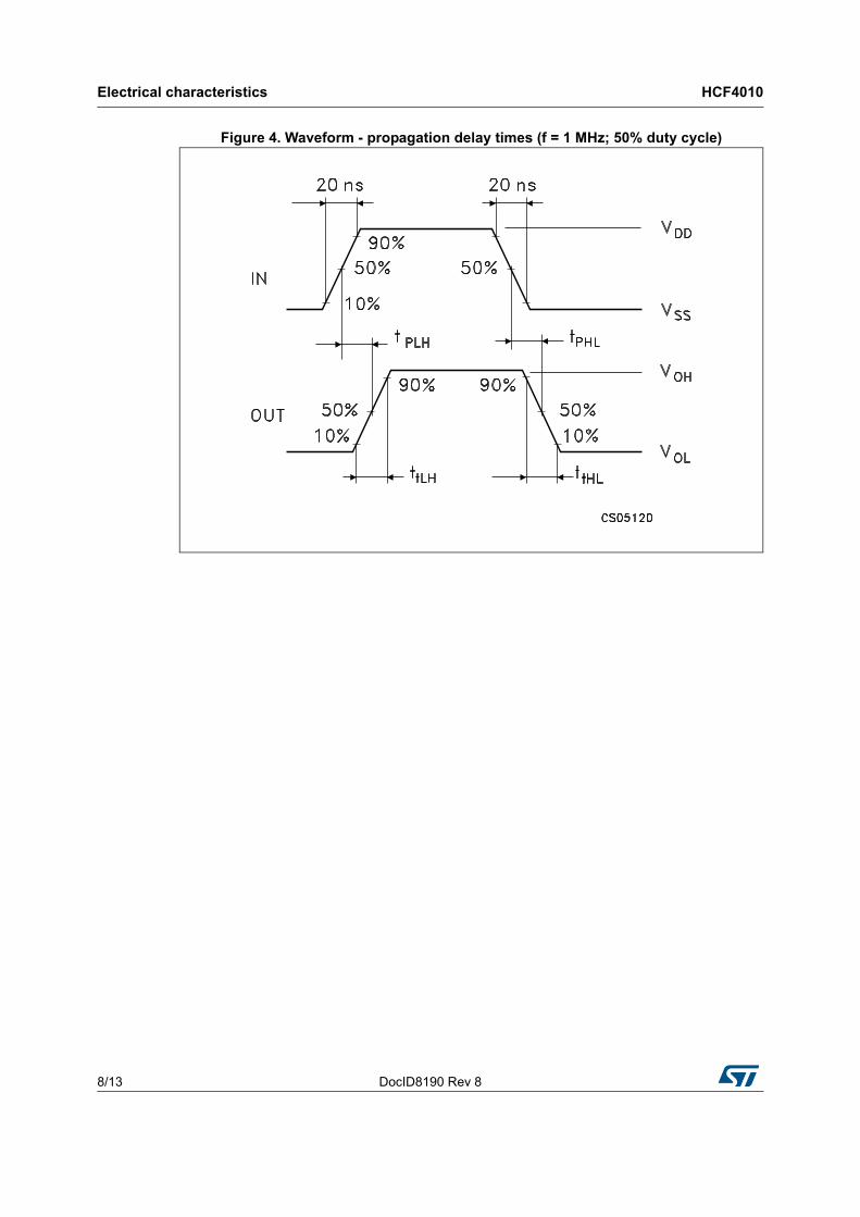
Figure 4. Waveform - propagation delay times (f = 1 MHz; 50% duty cycle)
DocID8190 Rev 8 9/13
HCF4010 Package information
13
4 Package information
In order to meet environmental requirements, ST offers these devices in different grades of ECOPACK® packages, depending on their level of environmental compliance. ECOPACK specifications, grade definitions and product status are available at: www.st.com. ECOPACK is an ST trademark.
Package information HCF4010
10/13 DocID8190 Rev 8
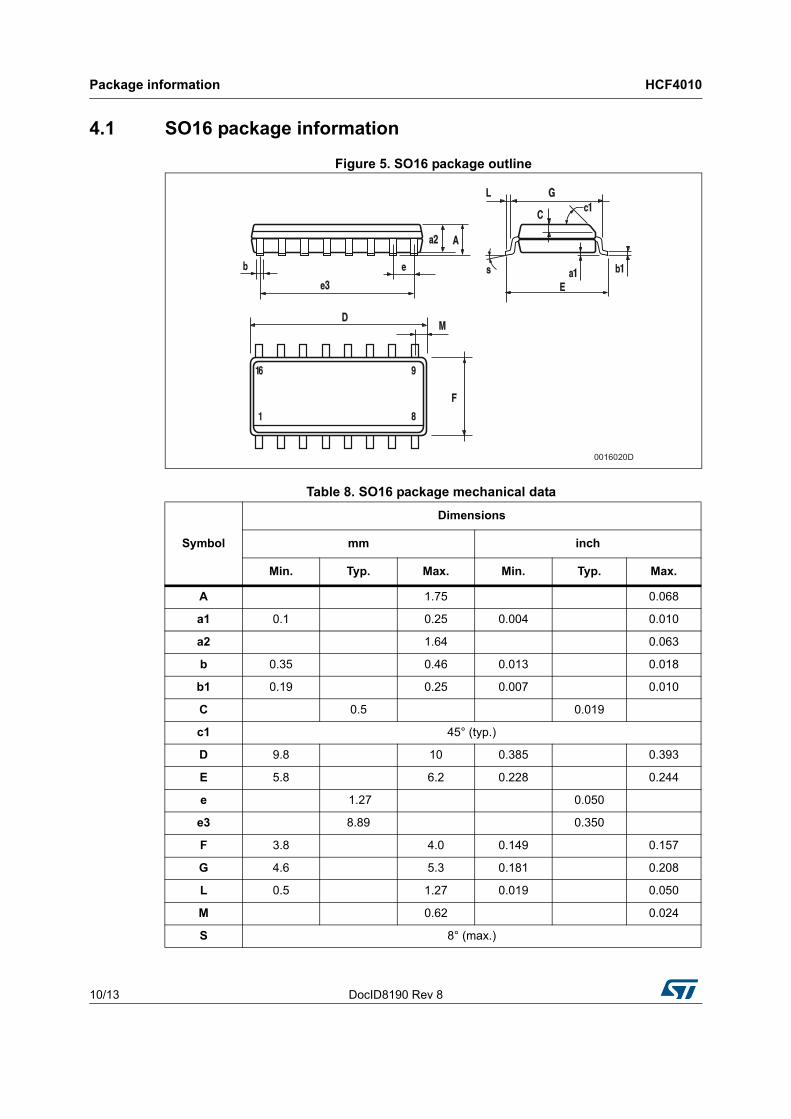
4.1 SO16 package information
Figure 5. SO16 package outline
Table 8. SO16 package mechanical data
Symbol
Dimensions
mm inch
Min. Typ. Max. Min. Typ. Max.
A 1.75 0.068
a1 0.1 0.25 0.004 0.010
a2 1.64 0.063
b 0.35 0.46 0.013 0.018
b1 0.19 0.25 0.007 0.010
C 0.5 0.019
c1 45° (typ.)
D 9.8 10 0.385 0.393
E 5.8 6.2 0.228 0.244
e 1.27 0.050
e3 8.89 0.350
F 3.8 4.0 0.149 0.157
G 4.6 5.3 0.181 0.208
L 0.5 1.27 0.019 0.050
M 0.62 0.024
S 8° (max.)
0016020D
DocID8190 Rev 8 11/13
HCF4010 Package information
13
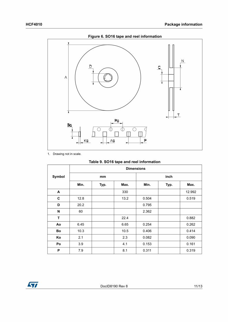
Figure 6. SO16 tape and reel information
1. Drawing not in scale.
.
Table 9. SO16 tape and reel information
Symbol
Dimensions
mm inch
Min. Typ. Max. Min. Typ. Max.
A 330 12.992
C 12.8 13.2 0.504 0.519
D 20.2 0.795
N 60 2.362
T 22.4 0.882
Ao 6.45 6.65 0.254 0.262
Bo 10.3 10.5 0.406 0.414
Ko 2.1 2.3 0.082 0.090
Po 3.9 4.1 0.153 0.161
P 7.9 8.1 0.311 0.319

Ordering information HCF4010
12/13 DocID8190 Rev 8
5 Ordering information
6 Revision history
Table 10. Order codes
Order code Temperature range Package Packing Marking
HCF4010M013TR –55 °C to +125 °C SO16Tape and
reel
HCF4010
HCF4010YM013TR(1)
1. Qualification and characterization according to AEC Q100 and Q003 or equivalent, advanced screening according to AEC Q001 and Q002 or equivalent.
–40 °C to +125 °CSO16
(automotive grade)HCF4010Y
Table 11. Document revision history
Date Revision Changes
16-Mar-2005 3 Add VCC on Table 6
11-Jun-2012 4
Added Applications on page 1
Updated Table 1: Device summary
Removed DIP16 package from document
Revised document presentation, minor textual updates
15-Jun-2012 5Updated temperature range in Table 1
Updated Top in Table 5
19-Oct-2012 6
Updated Features (added ESD data).
Updated Table 1 (added Marking, updated note 1.)
Reformatted Section 4 (added Figure 5 and Figure 6, Table 8 and Table 9).
Minor corrections throughout document.
25-Apr-2013 7Updated Features: ESD data modified, removed information regarding B series CMOS devices.
Added Section 5: Ordering information
13-Jan-2014 8 Table 1: Device summary: added “Packing”
DocID8190 Rev 8 13/13
HCF4010
13
Please Read Carefully:
Information in this document is provided solely in connection with ST products. STMicroelectronics NV and its subsidiaries (“ST”) reserve the right to make changes, corrections, modifications or improvements, to this document, and the products and services described herein at any time, without notice.
All ST products are sold pursuant to ST’s terms and conditions of sale.
Purchasers are solely responsible for the choice, selection and use of the ST products and services described herein, and ST assumes no liability whatsoever relating to the choice, selection or use of the ST products and services described herein.
No license, express or implied, by estoppel or otherwise, to any intellectual property rights is granted under this document. If any part of this document refers to any third party products or services it shall not be deemed a license grant by ST for the use of such third party products or services, or any intellectual property contained therein or considered as a warranty covering the use in any manner whatsoever of such third party products or services or any intellectual property contained therein.
UNLESS OTHERWISE SET FORTH IN ST’S TERMS AND CONDITIONS OF SALE ST DISCLAIMS ANY EXPRESS OR IMPLIED WARRANTY WITH RESPECT TO THE USE AND/OR SALE OF ST PRODUCTS INCLUDING WITHOUT LIMITATION IMPLIED WARRANTIES OF MERCHANTABILITY, FITNESS FOR A PARTICULAR PURPOSE (AND THEIR EQUIVALENTS UNDER THE LAWS OF ANY JURISDICTION), OR INFRINGEMENT OF ANY PATENT, COPYRIGHT OR OTHER INTELLECTUAL PROPERTY RIGHT.
ST PRODUCTS ARE NOT DESIGNED OR AUTHORIZED FOR USE IN: (A) SAFETY CRITICAL APPLICATIONS SUCH AS LIFE SUPPORTING, ACTIVE IMPLANTED DEVICES OR SYSTEMS WITH PRODUCT FUNCTIONAL SAFETY REQUIREMENTS; (B) AERONAUTIC APPLICATIONS; (C) AUTOMOTIVE APPLICATIONS OR ENVIRONMENTS, AND/OR (D) AEROSPACE APPLICATIONS OR ENVIRONMENTS. WHERE ST PRODUCTS ARE NOT DESIGNED FOR SUCH USE, THE PURCHASER SHALL USE PRODUCTS AT PURCHASER’S SOLE RISK, EVEN IF ST HAS BEEN INFORMED IN WRITING OF SUCH USAGE, UNLESS A PRODUCT IS EXPRESSLY DESIGNATED BY ST AS BEING INTENDED FOR “AUTOMOTIVE, AUTOMOTIVE SAFETY OR MEDICAL” INDUSTRY DOMAINS ACCORDING TO ST PRODUCT DESIGN SPECIFICATIONS. PRODUCTS FORMALLY ESCC, QML OR JAN QUALIFIED ARE DEEMED SUITABLE FOR USE IN AEROSPACE BY THE CORRESPONDING GOVERNMENTAL AGENCY.
Resale of ST products with provisions different from the statements and/or technical features set forth in this document shall immediately void any warranty granted by ST for the ST product or service described herein and shall not create or extend in any manner whatsoever, any liability of ST.
ST and the ST logo are trademarks or registered trademarks of ST in various countries.Information in this document supersedes and replaces all information previously supplied.
The ST logo is a registered trademark of STMicroelectronics. All other names are the property of their respective owners.
© 2014 STMicroelectronics - All rights reserved
STMicroelectronics group of companies
Australia - Belgium - Brazil - Canada - China - Czech Republic - Finland - France - Germany - Hong Kong - India - Israel - Italy - Japan - Malaysia - Malta - Morocco - Philippines - Singapore - Spain - Sweden - Switzerland - United Kingdom - United States of America
www.st.com
Recommended