Guide to DAQ SignAl ConneCtionS
mccdaq.com
THE VALUE LEADER IN DATA ACQUISITION

Measurement Computing • 10 Commerce Way • Norton, MA 02766 • (508) 946-5100 • [email protected] • mccdaq.com
2
ContentsTrademark and CopyrighT informaTion ........................................................................... 3
ChapTer 1analog input Types ...................................................................................................................................... 4Single-ended Inputs ........................................................................................................................................................................... 4
Differential Inputs .............................................................................................................................................................................. 4
ChapTer 2System grounds and isolation .................................................................................................................... 6Ground Type Determination ............................................................................................................................................................. 6
Systems with Common Grounds ....................................................................................................................................................... 6
Systems with Common Mode (Ground Offset) Voltages .................................................................................................................. 7
Small Common Mode Voltages ...................................................................................................................................................... 7
Large Common Mode Voltages ...................................................................................................................................................... 7
Device and Signal Source already have Isolated Grounds ................................................................................................................. 7
ChapTer 3Wiring Configurations ................................................................................................................................. 8Common Ground / Single-ended Inputs ........................................................................................................................................... 8
Common Ground / Differential Inputs ............................................................................................................................................. 9
Common Mode Voltage < ±10 V / Single-ended Inputs ................................................................................................................... 9
Common Mode Voltage < ±10 V / Differential Inputs ...................................................................................................................... 9
Common Mode Voltage > ±10 V / Single-ended Inputs ................................................................................................................. 10
Common Mode Voltage > ±10 V / Differential Inputs .................................................................................................................... 10
Isolated Grounds / Single-ended Inputs .......................................................................................................................................... 11
Isolated Grounds / Differential Inputs ............................................................................................................................................ 11
Analog Output Current Configuration ............................................................................................................................................ 12
ChapTer 4digital i/o Techniques ............................................................................................................................... 13Pull-up and Pull-down Resistors ...................................................................................................................................................... 13
TTL to Solid State Relays .................................................................................................................................................................. 14
Voltage Dividers ............................................................................................................................................................................... 14
Equation for Dissipation of Power in the Divider ........................................................................................................................... 14
Low-pass Filter to Debounce Inputs ................................................................................................................................................ 15
mCC daQ ..................................................................................................................................... 16

3
Measurement Computing • 10 Commerce Way • Norton, MA 02766 • (508) 946-5100 • [email protected] • mccdaq.com
Trademark and CopyrighT informaTionMeasurement Computing Corporation, InstaCal, Universal Library, and the Measurement Computing logo are either trademarks or registered trademarks of Measurement Computing Corporation. Refer to the Copyrights & Trademarks section on mccdaq.com/legal for more information about Measurement Computing trademarks. Other product and company names mentioned herein are trademarks or trade names of their respective companies.
© 2012 Measurement Computing Corporation. All rights reserved. No part of this publication may be reproduced, stored in a retrieval system, or transmitted, in any form by any means, electronic, mechanical, by photocopying, recording, or otherwise without the prior written permission of Measurement Computing Corporation.
Notice: Measurement Computing Corporation does not authorize any Measurement Computing Corporation product for use in life support systems and/or devices without prior written consent from Measurement Computing Corporation. Life support devices/systems are devices or systems that, a) are intended for surgical implantation into the body, or b) support or sustain life and whose failure to perform can be reasonably expected to result in injury. Measurement Computing Corporation products are not designed with the components required, and are not subject to the testing required to ensure a level of reliability suitable for the treatment and diagnosis of people.
© Copyright 2012, Measurement Computing Corporation Revision 5, September 2012
Measurement Computing • 10 Commerce Way • Norton, MA 02766 • (508) 946-5100 • [email protected] • mccdaq.com
4
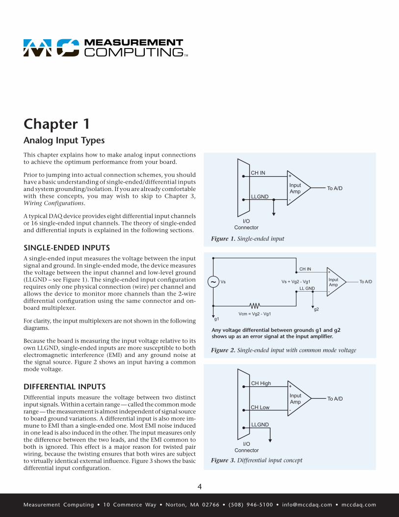
Chapter 1analog input TypesThis chapter explains how to make analog input connections to achieve the optimum performance from your board.
Prior to jumping into actual connection schemes, you should have a basic understanding of single-ended/differential inputs and system grounding/isolation. If you are already comfortable with these concepts, you may wish to skip to Chapter 3, Wiring Configurations.
A typical DAQ device provides eight differential input channels or 16 single-ended input channels. The theory of single-ended and differential inputs is explained in the following sections.
Single-ended inpuTSA single-ended input measures the voltage between the input signal and ground. In single-ended mode, the device measures the voltage between the input channel and low-level ground (LLGND – see Figure 1). The single-ended input configuration requires only one physical connection (wire) per channel and allows the device to monitor more channels than the 2-wire differential configuration using the same connector and on-board multiplexer.
For clarity, the input multiplexers are not shown in the following diagrams.
Because the board is measuring the input voltage relative to its own LLGND, single-ended inputs are more susceptible to both electromagnetic interference (EMI) and any ground noise at the signal source. Figure 2 shows an input having a common mode voltage.
differenTial inpuTSDifferential inputs measure the voltage between two distinct input signals. Within a certain range — called the common mode range — the measurement is almost independent of signal source to board ground variations. A differential input is also more im-mune to EMI than a single-ended one. Most EMI noise induced in one lead is also induced in the other. The input measures only the difference between the two leads, and the EMI common to both is ignored. This effect is a major reason for twisted pair wiring, because the twisting ensures that both wires are subject to virtually identical external influence. Figure 3 shows the basic differential input configuration.
Figure 2. Single-ended input with common mode voltage
Figure 1. Single-ended input
Figure 3. Differential input concept
CH IN
I/OConnector
InputAmp To A/D
+
-LLGND
CH High
CH Low
I/OConnector
InputAmp To A/D
+
-
LLGND
CH IN
g1
g2Vcm = Vg2 - Vg1
Vs + Vg2 - Vg1Vs InputAmp
To A/D
+
-LL GND
~
any voltage differential between grounds g1 and g2 shows up as an error signal at the input amplifier.

5
Measurement Computing • 10 Commerce Way • Norton, MA 02766 • (508) 946-5100 • [email protected] • mccdaq.com
Before describing grounding and isolation, it is important to explain the concepts of common mode voltage and common mode range. Common mode voltage is shown in Figure 4 as Vcm.
Although differential inputs measure the voltage between two signals — almost without respect to either of the signal voltages relative to ground — there is a voltage limit on the signal. Although the board has differential inputs, it cannot measure the difference between 13 V and 14 V as 1 V. The common mode voltage range of ±10 V is shown graphically in Figure 5. Even in differential mode, an input signal cannot be measured if it is more than 10 V from the board’s LLGND.
Figure 5. Common mode voltage = +4 V
Figure 4. Differential input voltages defined
CH High
DifferentialInput
g1 g2
Vcm
Vcm = Vg2 - Vg1
Vs
Vs CH Low
InputAmp
To A/D
+
-
LLGND
~
Common mode voltage (Vcm) is ignored in a differential input configuration. however, note that the Vcm + Vs must remain within the amplifier’s common mode range of ±10 V.
+13 V+12 V+11 V+10 V+9 V+8 V+7 V+6 V+5 V+4 V+3 V+2 V+1 V
With Vcm = +4 VDC, +Vs must be less than +6 V, or the common mode range will be exceeded (> +10 V)
Vcm
-1 V-2 V-3 V-4 V-5 V-6 V-7 V-8 V-9 V
-10 V-11 V-12 V-13 V
Guide to DAQ Signal Connections Chapter 1: Analog Input Types

Measurement Computing • 10 Commerce Way • Norton, MA 02766 • (508) 946-5100 • [email protected] • mccdaq.com
6
Chapter 2System grounds and isolationThere are three ways to connect a signal source to a DAQ device:
• The device input and the signal source have the same (or common) ground. This signal source can be connected directly to the device.
• The device input and the signal source have an offset voltage between their grounds (AC and/or DC). This offset is the common mode voltage. Depending on the magnitude of this voltage, you may be able to connect the device directly to your signal source. We will explain this later.
• The device and the signal source already have isolated grounds. You can connect this signal source directly to the device.
ground Type deTerminaTionIf possible, use a battery-powered voltmeter to measure the AC and DC voltages between the signal source ground and PC ground. If you do not have access to a battery-powered voltmeter, skip this test and read sections Systems with Common Grounds through Small Common Mode Voltages. You still may be able to identify your system type from the descriptions provided.
If both AC and DC readings are 0.000 V, you may have a system with common grounds. However, since voltmeters average out high frequency signals, there is no guarantee. Refer to the section Systems with Common Grounds.
If you measure reasonably stable AC and DC voltages, this offset is the common mode voltage. Refer to the section Systems with Common Mode (Ground Offset) Voltages.
Read the following caution carefully, and then proceed to the remaining sections in this chapter describing common mode systems.
Caution! For most Measurement Computing (MCC) DAQ devices, do not connect a device to a signal source if the AC or DC voltage is greater than 10 V, which is beyond the usable common mode range of the device. Either adjust the grounding system or add special isolation signal conditioning to take useful measurements.
A ground offset voltage of more than 30 V will likely damage the a device and possibly your computer. An offset voltage greater than 30 V will not only damage your electronics, but can be hazardous to you. In this case, either reconfigure your system to reduce the ground differentials, or install electrical isolation signal conditioning.
If you cannot obtain a reasonably stable DC voltage measurement between the grounds, or the voltage drifts around consider-ably, the two grounds are probably isolated. The easiest way to check for isolation is to change your voltmeter mode to resistance (use an ohm scale) and measure the resistance between the two grounds. Turn both systems OFF prior to taking this resistance measurement. If the measured resistance is greater than 100 kΩ, your system probably has electrically-isolated grounds.
SySTemS WiTh Common groundSIn the simplest but perhaps the least likely case, your signal source has the same ground potential as the device. This would typically occur when providing power or excitation to your signal source directly from the device. Any voltage between the device ground and your signal ground is a potential error voltage if you set up your system assuming there is a common ground.

7
Measurement Computing • 10 Commerce Way • Norton, MA 02766 • (508) 946-5100 • [email protected] • mccdaq.com
Guide to DAQ Signal Connections Chapter 2: System Grounds and Isolation
If your signal source or sensor is not connected directly to an LLGND pin on your device, it is best to assume that you do not have a common ground even if your voltmeter measures 0.0 V. Configure your system as if there is ground offset voltage between the source and the device. This is especially true if you are using high gains, since ground potentials in the sub-millivolt range are large enough to cause A/D errors, but may not be measured by your handheld voltmeter.
SySTemS WiTh Common mode (ground offSeT) VolTageS The most frequently encountered grounding scenario involves grounds that are somehow connected, but have offset voltages between the device and signal source grounds. This offset voltage may be AC, DC, or both. The offset can be caused by a wide array of phenomena, such as EMI pickup or resistive voltage drops in ground wiring and connections. Ground offset voltage is a more descriptive term for this type of system, but the term common mode is more frequently used (and is used in this document).
Small Common mode Voltages
If the voltage between the signal source ground and device ground is small, the combination of the ground voltage and input signal does not exceed the allowable ±10 V common mode range. Specifically, when you add the voltage between grounds to the maximum input voltage, the result is within ±10 V. This input is compatible with the device, and you can connect the system without additional signal conditioning. Fortunately, most systems fall into this category and have small voltage differentials between grounds.
large Common mode Voltages
If the ground differential is large enough, the allowable ±10 V does exceed the common mode range. Specifically, when you add the voltage between device and signal source grounds to the maximum input voltage you are trying to measure, the result exceeds ±10 V. In this case, do not connect the device directly to the signal source. You must change your system grounding configuration or add isolation signal conditioning. For more information, please review our ISO-RACK and ISO 5B-series products to add electri-cal isolation, or call our technical support group at to discuss other options.
Caution! Avoid using earth prong of a 120 VAC for signal ground connections. Do not rely on the earth prong of a 120 VAC for signal ground connections. Different ground plugs may have large and potentially even dangerous voltage differentials. Remember that the ground pins on 120 VAC outlets on different sides of the room may only be connected in the basement. This leaves the possibility that the ground pins may have a significant voltage differential — especially if the two 120 VAC outlets happen to be on different line phases.
deViCe and Signal SourCe already haVe iSolaTed groundSSome signal sources are already electrically isolated from the device. The diagram shown in Figure 6 shows a typical isolated ground system. These signal sources are often battery powered, or are complex equipment. Isolated ground systems provide excellent performance but require care to ensure you get optimum performance. Refer to Chapter 3 Wiring Configurations for more details.

Measurement Computing • 10 Commerce Way • Norton, MA 02766 • (508) 946-5100 • [email protected] • mccdaq.com
8
Chapter 3Wiring ConfigurationsAll grounding and input type combinations are summarized in the table below. These combinations and our recommended uses are given in the table.
Input Configuration Recommendations (based on a device with ±10 V common mode range)
ground Category input Configuration mCC recommendation
Common ground Single-ended inputs Recommended
Common ground Differential inputs Acceptable
Common mode voltage < ±10 V Single-ended inputs Not recommended
Common mode voltage < ±10 V Differential inputs Recommended
Common mode voltage > ±10 V Single-ended inputs Unacceptable without adding Isolation
Common mode voltage > ±10 V Differential inputs Unacceptable without adding Isolation
Already isolated grounds Single-ended inputs Acceptable
Already isolated grounds Differential inputs Recommended
The following sections contain recommended input wiring schemes for each of the acceptable input configuration/grounding combinations.
Common ground / Single-ended inpuTSSingle-ended is the recommended configuration for common ground connections. However, if some inputs are common ground and some are not, you should use the differential mode for all inputs. There is no performance penalty other than loss of channels for using a differential input rather than a single-ended input to measure a common ground signal source, though the reverse is not true. Figure 6 shows the recommended connections for a common ground / single-ended input system.
Figure 6. Common ground / single-ended input system
CH IN
I/OConnector
InputAmp To A/D
+
-
88 88:
+-
A/D Board
Optional wire since signal sourceand A/D board share common ground
LLGND
Signal Source with Common Gnd
Signal source and a/d board sharing common ground connected to single-ended input

9
Measurement Computing • 10 Commerce Way • Norton, MA 02766 • (508) 946-5100 • [email protected] • mccdaq.com
A/D Board
CH High
CH Low
I/OConnector
InputAmp To A/D
+
-
88 88:
+-
The voltage differentialbetween these grounds
added to the maximum inputsignal must stay within ±10 V
LLGND
GND
Signal Source with Common Mode Voltage
A/D Board
CH High
CH Low
I/OConnector
InputAmp To A/D
+
-
88 88:
+-
Optional wiresince signal source
and A/D board sharecommon ground
Required connectionof LLGND to CH Low
LLGND
Signal Source with Common Gnd
Common ground / differenTial inpuTSUsing differential inputs to monitor a signal source with a common ground is an acceptable configuration, though it requires more wiring and offers fewer channels than selecting a single-ended configuration. Figure 7 shows this configuration.
Common mode VolTage < ±10 V / Single-ended inpuTSThe phrase common mode has no meaning in a single-ended system, and this is not a recommended configuration. This case can be described as a system with offset grounds. You can try this configuration, and no system damage should occur. Depending on the overall accuracy you require, you may receive acceptable results.
Common mode VolTage < ±10 V / differenTial inpuTSSystems with varying ground potentials should always be monitored in the differential mode. Make sure that the sum of the input signal and the ground differential (referred to as the common mode voltage) does not exceed the common mode range of the A/D device (generally ±10 V). Figure 8 shows recommended connections in this configuration.
Figure 7. Common ground / differential inputs
Figure 8. Common mode / differential inputs (< ±10 V) common mode voltage
Guide to DAQ Signal Connections Chapter 3: Wiring Configurations
Signal source and a/d board sharing common ground connected to a differential input
Signal source and a/d board sharing common mode voltage connected to differential input

10
Measurement Computing • 10 Commerce Way • Norton, MA 02766 • (508) 946-5100 • [email protected] • mccdaq.com
A/D Board
CH IN
I/OConnector
InputAmp To A/D
+
-
88 88:
+-
LLGND
GND
Large common mode voltage betweensignal source and A/D board
When the voltage difference betweenthe signal source and A/D board ground
is so large that the A/D board’s common mode range is exceeded,
isolated signal conditioning must be added
Isolation Barrier
A/D Board
CH High
CH Low
I/OConnector
InputAmp To A/D
+
-
88 88:
+-
LLGND
GND
Large Common Mode Voltage betweenSignal Source and A/D Board
10K
10K is a recommended value. You may short LLGND to CH Lowinstead, but this will reduce your system’s noise immunity.
When the voltage difference betweenthe signal source and A/D board ground
is so large that the A/D board’s common mode range is exceeded,
isolated signal conditioning must be added
Most MCC devices cannot directly monitor signals with common mode voltages greater than ±10 V. Alter the system ground configuration to reduce the overall common mode voltage, or add isolated signal conditioning between the source and the device (Figure 9 and Figure 10).
Common mode VolTage > ±10 V / Single-ended inpuTS
Figure 9. Common mode voltage > ±10 V single-ended input
Figure 10. Common mode voltage > ±10 V differential input
Guide to DAQ Signal Connections Chapter 3: Wiring Configurations
System with a large common mode voltage connected to a single-ended input
System with a large common mode voltage connected to a differential input
Common mode VolTage > ±10 V / differenTial inpuTS

11
Measurement Computing • 10 Commerce Way • Norton, MA 02766 • (508) 946-5100 • [email protected] • mccdaq.com
A/D Board
CH High
CH Low
I/OConnector
InputAmp To A/D
+
-
88 88:
+-
LLGND
GND
Signal Source and A/D Board Already Isolated
10K
10K is a recommended value. You may short LLGND to CH Lowinstead, but this will reduce your system’s noise immunity.
These grounds are electrically isolated
A/D Board
CH IN
I/OConnector
InputAmp To A/D
+
-
88 88:
+-
LLGND
Isolated Signal Source
iSolaTed groundS / Single-ended inpuTSYou can use single-ended inputs to monitor isolated inputs, although using differential mode increases your system’s noise immunity. Figure 11 shows the recommended connections in this configuration.
Figure 11. Isolated grounds / single-ended inputs
Figure 12. Isolated grounds / differential inputs
iSolaTed groundS / differenTial inpuTSTo ensure optimum performance with isolated signal sources, use the differential input setting. Figure 12 shows the recommended connections for this configuration.
Guide to DAQ Signal Connections Chapter 3: Wiring Configurations
isolated signal source connected to a single-ended input
isolated signal source and a/d board connected to a differntial input

12
Measurement Computing • 10 Commerce Way • Norton, MA 02766 • (508) 946-5100 • [email protected] • mccdaq.com
Connection withGrounded Load
Connection with Grounded Supply
GroundedExternalSupply
+IOUTn
AGND
Floating LoadIOUTn
IOUTn+1
IOUTn+2
Floating LoadIOUTn+1
Floating LoadIOUTn+2
IOUTn
AGND
GroundedLoad
IOUTn+1
IOUTn+2
+ Floating Supply IOUTn+1
Floating Ext.Supply
+ Floating Supply IOUTn+1
Floating Ext.Supply
+ Floating Supply IOUTn+1
Floating Ext.Supply
IOU
Tn+2
IOU
Tn
IOU
Tn+1
IOUTn+1
IOUTn+2
IOUTn
Figure 13. Typical analog current output circuit
analog ouTpuT CurrenT ConfiguraTionFigure 13 shows a typical analog current output circuit. You should check the specs of the current output DAQ device to ensure that your circuit meets the minimum voltage available at IOUTn, and also that it does not exceed the maximum external excitation voltage used to power the loop.
A typical application uses a 24 V loop supply. The loop can use either a grounded load where the supply floats, or a grounded supply where the load floats. Each connection method is shown here.
Refer to the manufacturer’s information for the device being controlled for additional details.
Guide to DAQ Signal Connections Chapter 3: Wiring Configurations
Measurement Computing • 10 Commerce Way • Norton, MA 02766 • (508) 946-5100 • [email protected] • mccdaq.com
13
+5 V
R
ControlledDevice
Digital I/ODevice
A0
Pull-Up Current Sinking = 5 VR
Chapter 4digital i/o TechniquesThis chapter explains a few digital I/O application techniques often needed by DAQ device users. It covers a few key application techniques used with digital I/O.
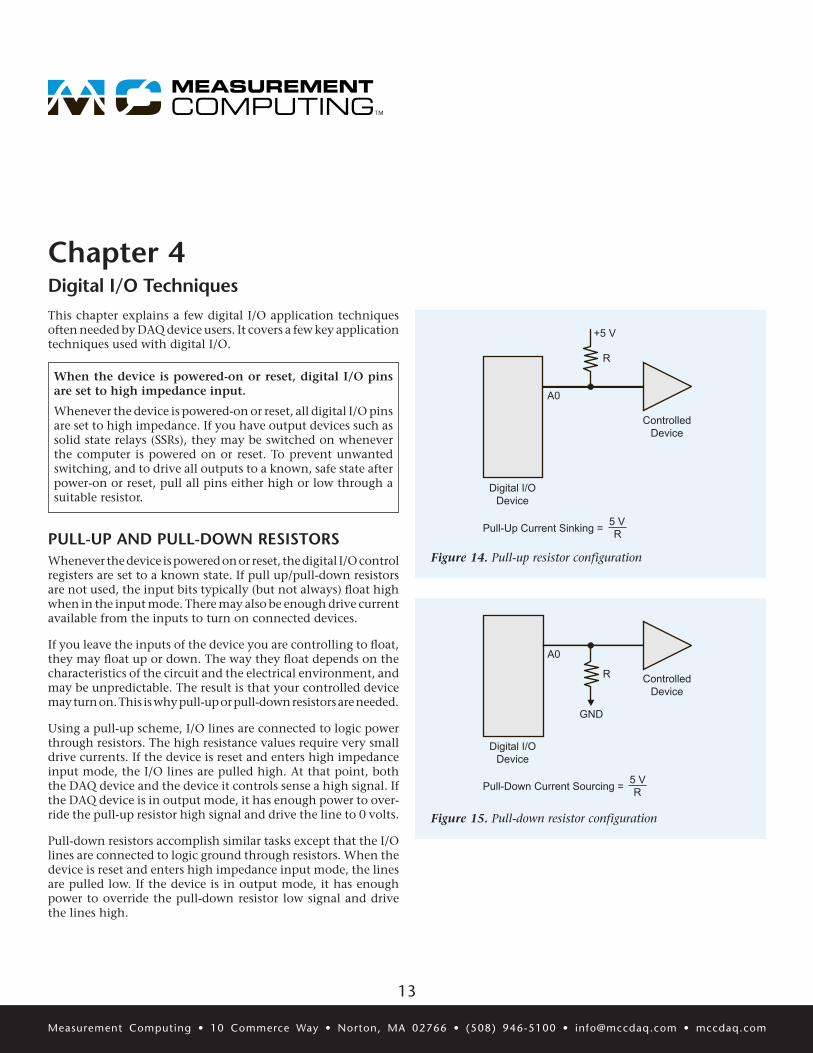
When the device is powered-on or reset, digital I/O pins are set to high impedance input.
Whenever the device is powered-on or reset, all digital I/O pins are set to high impedance. If you have output devices such as solid state relays (SSRs), they may be switched on whenever the computer is powered on or reset. To prevent unwanted switching, and to drive all outputs to a known, safe state after power-on or reset, pull all pins either high or low through a suitable resistor.
pull-up and pull-doWn reSiSTorSWhenever the device is powered on or reset, the digital I/O control registers are set to a known state. If pull up/pull-down resistors are not used, the input bits typically (but not always) float high when in the input mode. There may also be enough drive current available from the inputs to turn on connected devices.
If you leave the inputs of the device you are controlling to float, they may float up or down. The way they float depends on the characteristics of the circuit and the electrical environment, and may be unpredictable. The result is that your controlled device may turn on. This is why pull-up or pull-down resistors are needed.
Using a pull-up scheme, I/O lines are connected to logic power through resistors. The high resistance values require very small drive currents. If the device is reset and enters high impedance input mode, the I/O lines are pulled high. At that point, both the DAQ device and the device it controls sense a high signal. If the DAQ device is in output mode, it has enough power to over-ride the pull-up resistor high signal and drive the line to 0 volts.
Pull-down resistors accomplish similar tasks except that the I/O lines are connected to logic ground through resistors. When the device is reset and enters high impedance input mode, the lines are pulled low. If the device is in output mode, it has enough power to override the pull-down resistor low signal and drive the lines high.
Figure 14. Pull-up resistor configuration
GND
R ControlledDevice
Digital I/ODevice
A0
Pull-Down Current Sourcing = 5 VR
Figure 15. Pull-down resistor configuration

14
Measurement Computing • 10 Commerce Way • Norton, MA 02766 • (508) 946-5100 • [email protected] • mccdaq.com
Vout = R2 * VinR1 + R2
Signal High
Signal Low
BoardInput
V2Vout
V1
Vin
Ground
Signal Volts
R1
R2
TTl To Solid STaTe relaySMany applications require digital outputs to switch high AC and DC voltages on and off and to monitor high AC and DC voltages. These high voltages cannot be controlled or read directly by the TTL digital lines of a device.
SSRs – such as those available from MCC – allow you to con-trol and monitor AC and high DC voltages and provide 750 V isolation. SSRs are the recommended method of interfacing to AC and high DC signals.
The most convenient way to use SSRs is to purchase an SSR rack, which is a circuit device that has sockets for SSRs and buffer amplifiers powerful enough to switch the SSRs. SSR racks are available from MCC and most manufacturers of SSRs. If you have only a few outputs to control, you may also wish to consider the DR-OAC or DR-ODC, single point, DIN mountable SSRs.
VolTage diViderSIf you need to detect a signal that varies over a range greater than the maximum input specification of a digital input, you must use a voltage divider or some other external device to reduce the voltage of the input signal to a safe level.
Ohm’s law states:
Voltage = Current x Resistance
In a voltage divider, the voltage across one of the resistors in a circuit is proportional to the resistance to the total resistance in the circuit.
The object in using a voltage divider is to choose two resistors with the proper proportions relative to the full value of the input voltage to the desired output voltage to the device input.
Dropping the voltage proportionally is called attenuation. The formula for attenuation is shown in the table below.
Digital inputs often require voltage dividers. For example, if you wish to detect a field signal that is at 0 V when OFF and 24 V when ON, you cannot connect that directly to the device’s digital
Figure 16. Voltage divider schematic
Attenuation Formula
inputs. The voltage must be dropped to 5 V maximum when ON. The attenuation required is 24:5 or 4.8. Use the equation above to find an appropriate R1 if R2 is 1K. Remember that a TTL input is ON when the input voltage is greater than 2.5 V.
eQuaTion for diSSipaTion of poWer in The diViderThe resistors, R1 and R2, are going to dissipate all the power in the divider circuit according to the equation:
Current = Voltage / Resistance.
The higher the value of the resistance (R1 + R2), the less power dissipated by the divider circuit.
As a simple rule:
• For attenuation of 5:1 or less, no resistor should be less than 10K.
• For attenuation of greater than 5:1, no resistor should be less than 1K.
Guide to DAQ Signal Connections Chapter 4: Digital I/O Techniques
Attenuation = R1+R2 R2
The variable attenuation is the proportional difference between the desired output voltage (max. input device input voltage) and the full input voltage from the field device.
2 = 10 KΩ +10 KΩ 10 KΩ
For example, if the field voltage varies between 0 V and 10 V and you wish to detect that with a maxi-mum device input voltage of 5 V, the Attenuation must be 2:1 or simply 2.
R1 = (A-1) x R2 For a given attenuation, pick a handy resistor and call it R2, then use this formula to calculate R1.

15
Measurement Computing • 10 Commerce Way • Norton, MA 02766 • (508) 946-5100 • [email protected] • mccdaq.com
Signal High
BoardHigh Input
BoardLow Input
SignalLow
Signal Volts
Low Pass Filter - Fc = 1
2 � RC
CR
loW-paSS filTer To de-bounCe inpuTSA low-pass filter is placed on the signal wires between a source and the device. It prevents frequencies greater than the cut-off frequency from entering the device’s digital inputs.
The cut-off frequency is the frequency above which no varia-tion of voltage, with respect to time, may enter the circuit. For example, if a low-pass filter had a cut-off frequency of 30 Hz, the interference associated with line voltage (60 Hz) would be mostly filtered out but a signal of 25 Hz would pass with less attenuation.
In a digital circuit, a low pass filter might be used to debounce (filter) an input from a switch or external relay. Unless switch/relay contacts are mercury-whetted, they tend to bounce briefly on closure, generating a pulsating noise signal. A simple low-pass filter can be constructed from one resistor (R) and one capacitor (C) (refer to Figure 17).
The cut-off frequency is determined according to the formula:
measurement Computing Corporation10 Commerce WayNorton, MA 02766
Phone: (508) 946-5100Fax: (508) 946-9500
E-mail: [email protected]
Figure 17. Low-pass filter schematic
Guide to DAQ Signal Connections Chapter 4: Digital I/O Techniques
1 2 π R C
1 2 π C Fc
Where π = 3.14... R = ohms C = farads Fc = cut-off frequency in cycles/second R =
Fc =

16
Measurement Computing • 10 Commerce Way • Norton, MA 02766 • (508) 946-5100 • [email protected] • mccdaq.com
MCC DAQ THE BEST VALUE IN THE INDUSTRY
DIgITAL I/O BOARDS AND DEVICESuSb-dio24 Series & dio96h• 24 or 96 TTL channels
• High-current output models available
• Included software & drivers
HIgH-SpEED, MULTIfUNCTION BOARDSuSb-2500 Series• 1 MS/s sampling
• 16-bit resolution
• Up to 64 analog inputs
• 24 digital I/O, 4 counters
• Up to 4 analog outputs
• Included software & drivers
SOLUTION HIgHLIgHTSMeasurement Computing DAQ devices are engineered to fit a wide array of applications. We offer USB, PCI/PCIe, Stand-alone loggers and Ethernet-based products.
Acquire data without programming with our included software support, or use one of many supported applications or programming languages.
LOwEST COST DEVICESuSb-Temp & TC Series• Measure thermocouples,
RTDs, thermistors, or voltage
• 24-bit resolution
• 8 channels
• Included software & drivers
HIgH-SpEED, STAND-ALONE DATA LOggERSlgr-5320 Series• 16 channels, up to ±30 V
• Up to 200 kS/s sampling
• 16 digital inputs up to 30 V
• Form C relay output
• 4 encoder inputs (quadrature available)
• 4 GB SD memory card
HIgH-ACCURACY, MULTIfUNCTION DEVICESuSb-2408 & 2416 Series• Measure thermocouples
or voltage
• 24-bit resolution
• 16 SE/8 DIFF or 32 SE/16 DIFF
• Up to 4 analog outputs, digital I/O, counters
• Included software & drivers
LOw-COST MULTIfUNCTION MODULESuSb-1208, 1408, 1608 Series• Up to 8 analog inputs
• 12-, 14-, or 16-bit resolution
• Up to 200 kS/s sampling
• Digital I/O, counters/timers
• Up to 2 analog outputs
• Included software & drivers
Recommended